Embed Size (px)
Citation preview

Input Voltage (V)
On-
Res
ista
nce
(m:
)
1 1.5 2 2.5 3 3.5 4 4.5 5 5.530
40
50
60
70
80
90
100
D001
-40qC25qC85qC105qC
OFF
ON
TPS22918
PowerSupply
VIN VOUT
CL
RL
GND
CT
CIN
ON
QOD
REXT
Product
Folder
Order
Now
Technical
Documents
Tools &
Software
Support &Community
An IMPORTANT NOTICE at the end of this data sheet addresses availability, warranty, changes, use in safety-critical applications,intellectual property matters and other important disclaimers. PRODUCTION DATA.
TPS22918SLVSD76C –FEBRUARY 2016–REVISED JULY 2017
TPS22918 5.5-V, 2-A, 52-mΩ On-Resistance Load Switch
1
1 Features1• Integrated Single Channel Load Switch• Ambient Operating Temperature: –40°C to
+105°C• Input Voltage Range: 1 V to 5.5 V• On-Resistance (RON)
– RON = 52 mΩ (typical) at VIN = 5 V– RON = 53 mΩ (typical) at VIN = 3.3 V
• 2-A Maximum Continuous Switch Current• Low Quiescent Current
– 8.3 µA (typical) at VIN = 3.3 V• Low-Control Input-Threshold Enables Use of 1 V
or Higher GPIO• Adjustable Quick-Output Discharge (QOD)• Configurable Rise Time With CT Pin• Small SOT23-6 Package (DBV)
– 2.90-mm × 2.80-mm, 0.95-mm Pitch,1.45 mm Height (with leads)
• ESD Performance Tested per JESD 22– ±2-kV HBM and ±1-kV CDM
2 Applications• Industrial Systems• Set Top Box• Blood Glucose Meters• Electronic Point of Sale
3 DescriptionThe TPS22918 is a single-channel load switch withconfigurable rise time and configurable quick outputdischarge. The device contains an N-channelMOSFET that can operate over an input voltagerange of 1 V to 5.5 V and can support a maximumcontinuous current of 2 A. The switch is controlled byan on and off input, which is capable of interfacingdirectly with low-voltage control signals.
The configurable rise time of the device greatlyreduces inrush current caused by large bulk loadcapacitances, thereby reducing or eliminating powersupply droop. The TPS22918 features a configurablequick output discharge (QOD) pin, which controls thefall time of the device to allow design flexibility forpower down and sequencing.
The TPS22918 is available in a small, leaded SOT-23package (DBV) which allows visual inspection ofsolder joints. The device is characterized foroperation over the free-air temperature range of–40°C to +105°C.
Device Information (1)
PART NUMBER PACKAGE BODY SIZE (NOM)TPS22918 SOT-23 (6) 2.90 mm × 1.60 mm
(1) For all available packages, see the orderable addendum atthe end of the datasheet.
Simplified Schematic On-Resistance vs Input VoltageTypical Values
IOUT = –200 mA

2
TPS22918SLVSD76C –FEBRUARY 2016–REVISED JULY 2017 www.ti.com
Product Folder Links: TPS22918
Submit Documentation Feedback Copyright © 2016–2017, Texas Instruments Incorporated
Table of Contents1 Features .................................................................. 12 Applications ........................................................... 13 Description ............................................................. 14 Revision History..................................................... 25 Pin Configuration and Functions ......................... 36 Specifications......................................................... 4
6.1 Absolute Maximum Ratings ...................................... 46.2 ESD Ratings ............................................................ 46.3 Recommended Operating Conditions....................... 46.4 Thermal Information .................................................. 46.5 Electrical Characteristics........................................... 56.6 Switching Characteristics .......................................... 66.7 Typical DC Characteristics........................................ 76.8 Typical AC Characteristics........................................ 9
7 Parameter Measurement Information ................ 118 Detailed Description ............................................ 12
8.1 Overview ................................................................. 128.2 Functional Block Diagram ....................................... 12
8.3 Feature Description................................................. 138.4 Device Functional Modes........................................ 15
9 Application and Implementation ........................ 169.1 Application Information............................................ 169.2 Typical Application ................................................. 16
10 Power Supply Recommendations ..................... 2011 Layout................................................................... 20
11.1 Layout Guidelines ................................................. 2011.2 Layout Example .................................................... 2111.3 Thermal Considerations ........................................ 21
12 Device and Documentation Support ................. 2212.1 Device Support...................................................... 2212.2 Documentation Support ........................................ 2212.3 Community Resources.......................................... 2212.4 Trademarks ........................................................... 2212.5 Electrostatic Discharge Caution............................ 2212.6 Glossary ................................................................ 22
13 Mechanical, Packaging, and OrderableInformation ........................................................... 22
4 Revision HistoryNOTE: Page numbers for previous revisions may differ from page numbers in the current version.
Changes from Revision A (March 2016) to Revision B Page
• Updated the constant value in Equation 3 in Adjustable Rise Time (CT) section................................................................ 14
Changes from Revision B (June 2016) to Revision C Page
• Updated the Applications Section changed µF to pF in Figure 30, Figure 31, and Section 9.2.2.5 ...................................... 1
Changes from Original (February 2016) to Revision A Page
• Changed device status from Product Preview to Production Data ........................................................................................ 1

1 VOUT
2 QOD
3 CT4ON
5GND
6VIN
3
TPS22918www.ti.com SLVSD76C –FEBRUARY 2016–REVISED JULY 2017
Product Folder Links: TPS22918
Submit Documentation FeedbackCopyright © 2016–2017, Texas Instruments Incorporated
5 Pin Configuration and Functions
DBV Package6-Pin SOT-23
Top View
Pin FunctionsPIN
I/O DESCRIPTIONNO. NAME
1 VIN I Switch input. Place ceramic bypass capacitor(s) between this pin and GND. See theDetailed Description section for more information.
2 GND — Device ground.3 ON I Active high switch control input. Do not leave floating.
4 CT O Switch slew rate control. Can be left floating. See the Feature Description section formore information.
5 QOD O
Quick Output Discharge pin. This functionality can be enabled in one of three ways.• Placing an external resistor between VOUT and QOD• Tying QOD directly to VOUT and using the internal resistor value (RPD)• Disabling QOD by leaving pin floatingSee the Quick Output Discharge (QOD) section for more information.
6 VOUT O Switch output.
4
TPS22918SLVSD76C –FEBRUARY 2016–REVISED JULY 2017 www.ti.com
Product Folder Links: TPS22918
Submit Documentation Feedback Copyright © 2016–2017, Texas Instruments Incorporated
(1) Stresses beyond those listed under Absolute Maximum Ratings may cause permanent damage to the device. These are stress ratingsonly, which do not imply functional operation of the device at these or any other conditions beyond those indicated under RecommendedOperating Conditions. Exposure to absolute-maximum-rated conditions for extended periods may affect device reliability.
(2) All voltage values are with respect to network ground terminal.
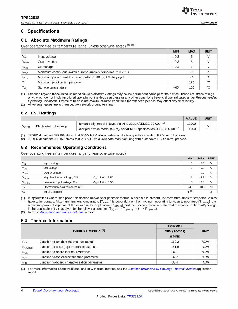
6 Specifications
6.1 Absolute Maximum RatingsOver operating free-air temperature range (unless otherwise noted) (1) (2)
MIN MAX UNITVIN Input voltage –0.3 6 VVOUT Output voltage –0.3 6 VVON ON voltage –0.3 6 VIMAX Maximum continuous switch current, ambient temperature = 70°C 2 AIPLS Maximum pulsed switch current, pulse < 300 µs, 2% duty cycle 2.5 ATJ Maximum junction temperature 125 °CTstg Storage temperature –65 150 °C
(1) JEDEC document JEP155 states that 500-V HBM allows safe manufacturing with a standard ESD control process.(2) JEDEC document JEP157 states that 250-V CDM allows safe manufacturing with a standard ESD control process.
6.2 ESD RatingsVALUE UNIT
V(ESD) Electrostatic dischargeHuman-body model (HBM), per ANSI/ESDA/JEDEC JS-001 (1) ±2000
VCharged-device model (CDM), per JEDEC specification JESD22-C101 (2) ±1000
(1) In applications where high power dissipation and/or poor package thermal resistance is present, the maximum ambient temperature mayhave to be derated. Maximum ambient temperature [TA(max)] is dependent on the maximum operating junction temperature [TJ(MAX)], themaximum power dissipation of the device in the application [PD(MAX)], and the junction-to-ambient thermal resistance of the part/packagein the application (θJA), as given by the following equation: TA(MAX) = TJ(MAX) – (θJA × PD(MAX)).
(2) Refer to Application and Implementation section
6.3 Recommended Operating ConditionsOver operating free-air temperature range (unless otherwise noted)
MIN MAX UNIT
VIN Input voltage 0 5.5 V
VON ON voltage 0 5.5 V
VOUT Output voltage VIN V
VIH, ON High-level input voltage, ON VIN = 1 V to 5.5 V 1 5.5 V
VIL, ON Low-level input voltage, ON VIN = 1 V to 5.5 V 0 0.5 V
TA Operating free-air temperature (1) –40 105 °C
CIN Input Capacitor 1 (2) µF
(1) For more information about traditional and new thermal metrics, see the Semiconductor and IC Package Thermal Metrics applicationreport.
6.4 Thermal Information
THERMAL METRIC (1)TPS22918
UNITDBV (SOT-23)6 PINS
RθJA Junction-to-ambient thermal resistance 183.2 °C/WRθJC(top) Junction-to-case (top) thermal resistance 151.6 °C/WRθJB Junction-to-board thermal resistance 34.1 °C/WψJT Junction-to-top characterization parameter 37.2 °C/WψJB Junction-to-board characterization parameter 33.6 °C/W

5
TPS22918www.ti.com SLVSD76C –FEBRUARY 2016–REVISED JULY 2017
Product Folder Links: TPS22918
Submit Documentation FeedbackCopyright © 2016–2017, Texas Instruments Incorporated
(1) Output pull down resistance varies with input voltage. Please see Figure 7 for more information.
6.5 Electrical CharacteristicsUnless otherwise noted, the specification in the following table applies over the full ambient operating temperature–40°C ≤ TA ≤ +105°C. Typical values are for TA = 25°C.
PARAMETER TEST CONDITIONS TA MIN TYP MAX UNIT
IQ, VIN Quiescent current VON = 5 V, IOUT = 0 A
VIN = 5.5 V
–40°C to +105°C
9.2 16
µA
VIN = 5 V 8.7 16VIN = 3.3 V 8.3 15VIN = 1.8 V 10.2 17VIN = 1.2 V 9.3 16VIN = 1 V 8.9 15
ISD, VIN Shutdown current VON = 0 V, VOUT = 0 V
VIN = 5.5 V
–40°C to +105°C
0.5 5
µA
VIN = 5 V 0.5 4.5VIN = 3.3 V 0.5 3.5VIN = 1.8 V 0.5 2.5VIN = 1.2 V 0.4 2VIN = 1 V 0.4 2
IONON pin inputleakage current VIN = 5.5 V, IOUT = 0 A –40°C to +105°C 0.1 µA
RON On-Resistance
VIN = 5.5 V, IOUT = –200 mA25°C 51 59
mΩ–40°C to +85°C 71–40°C to +105°C 78
VIN = 5.0 V, IOUT = –200 mA25°C 52 59
mΩ–40°C to +85°C 71–40°C to +105°C 79
VIN = 4.2 V, IOUT = –200 mA25°C 52 59
mΩ–40°C to +85°C 71–40°C to +105°C 79
VIN = 3.3 V, IOUT = –200 mA25°C 53 59
mΩ–40°C to +85°C 71–40°C to +105°C 80
VIN = 2.5 V, IOUT = –200 mA25°C 53 61
mΩ–40°C to +85°C 75–40°C to +105°C 80
VIN = 1.8 V, IOUT = –200 mA25°C 55 65
mΩ–40°C to +85°C 79–40°C to +105°C 88
VIN = 1.2 V, IOUT = –200 mA25°C 64 77
mΩ–40°C to +85°C 88–40°C to +105°C 104
VIN = 1.0 V, IOUT = –200 mA25°C 71 85
mΩ–40°C to +85°C 100–40°C to +105°C 116
VHYS ON pin hysteresis VIN = 1 V to 5.5 V –40°C to +105°C 107 mV
RPDOutput pull downresistance (1)
VIN = 5.0 V, VON = 0 V25°C 24
Ω
–40°C to +105°C 30
VIN = 3.3 V, VON = 0 V25°C 25–40°C to +105°C 35
VIN = 1.8 V, VON = 0 V25°C 45–40°C to +105°C 60
6
TPS22918SLVSD76C –FEBRUARY 2016–REVISED JULY 2017 www.ti.com
Product Folder Links: TPS22918
Submit Documentation Feedback Copyright © 2016–2017, Texas Instruments Incorporated
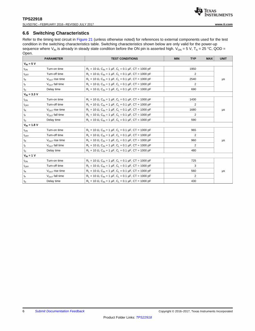
6.6 Switching CharacteristicsRefer to the timing test circuit in Figure 21 (unless otherwise noted) for references to external components used for the testcondition in the switching characteristics table. Switching characteristics shown below are only valid for the power-upsequence where VIN is already in steady state condition before the ON pin is asserted high. VON = 5 V, TA = 25 °C, QOD =Open.
PARAMETER TEST CONDITIONS MIN TYP MAX UNIT
VIN = 5 V
tON Turn-on time RL = 10 Ω, CIN = 1 µF, CL = 0.1 µF, CT = 1000 pF 1950
µs
tOFF Turn-off time RL = 10 Ω, CIN = 1 µF, CL = 0.1 µF, CT = 1000 pF 2
tR VOUT rise time RL = 10 Ω, CIN = 1 µF, CL = 0.1 µF, CT = 1000 pF 2540
tF VOUT fall time RL = 10 Ω, CIN = 1 µF, CL = 0.1 µF, CT = 1000 pF 2
tD Delay time RL = 10 Ω, CIN = 1 µF, CL = 0.1 µF, CT = 1000 pF 690
VIN = 3.3 V
tON Turn-on time RL = 10 Ω, CIN = 1 µF, CL = 0.1 µF, CT = 1000 pF 1430
µs
tOFF Turn-off time RL = 10 Ω, CIN = 1 µF, CL = 0.1 µF, CT = 1000 pF 2
tR VOUT rise time RL = 10 Ω, CIN = 1 µF, CL = 0.1 µF, CT = 1000 pF 1680
tF VOUT fall time RL = 10 Ω, CIN = 1 µF, CL = 0.1 µF, CT = 1000 pF 2
tD Delay time RL = 10 Ω, CIN = 1 µF, CL = 0.1 µF, CT = 1000 pF 590
VIN = 1.8 V
tON Turn-on time RL = 10 Ω, CIN = 1 µF, CL = 0.1 µF, CT = 1000 pF 965
µs
tOFF Turn-off time RL = 10 Ω, CIN = 1 µF, CL = 0.1 µF, CT = 1000 pF 2
tR VOUT rise time RL = 10 Ω, CIN = 1 µF, CL = 0.1 µF, CT = 1000 pF 960
tF VOUT fall time RL = 10 Ω, CIN = 1 µF, CL = 0.1 µF, CT = 1000 pF 2
tD Delay time RL = 10 Ω, CIN = 1 µF, CL = 0.1 µF, CT = 1000 pF 480
VIN = 1 V
tON Turn-on time RL = 10 Ω, CIN = 1 µF, CL = 0.1 µF, CT = 1000 pF 725
µs
tOFF Turn-off time RL = 10 Ω, CIN = 1 µF, CL = 0.1 µF, CT = 1000 pF 3
tR VOUT rise time RL = 10 Ω, CIN = 1 µF, CL = 0.1 µF, CT = 1000 pF 560
tF VOUT fall time RL = 10 Ω, CIN = 1 µF, CL = 0.1 µF, CT = 1000 pF 2
tD Delay time RL = 10 Ω, CIN = 1 µF, CL = 0.1 µF, CT = 1000 pF 430
Output Current (A)
On-
Res
ista
nce
(m:
)
0.2 0.4 0.6 0.8 1 1.2 1.4 1.6 1.8 20
10
20
30
40
50
60
70
80
90
100
D005
VIN= 1 VVIN = 1.2 VVIN = 1.5 V
VIN = 1.8 VVIN = 2.5 VVIN = 3.3 V
VIN = 4.2 VVIN = 5 VVIN = 5.5 V
Input Voltage (V)
Hys
tere
sis
Vol
tage
(m
V)
1 1.5 2 2.5 3 3.5 4 4.5 5 5.50
20
40
60
80
100
120
140
D008
-40qC25qC85qC105qC
Temperature (qC)
On-
Res
ista
nce
(m:
)
-40 -20 0 20 40 60 80 10020
30
40
50
60
70
80
90
100
D004
VIN= 1 VVIN = 1.05 VVIN = 1.2 V
VIN = 1.8 VVIN = 2.5 VVIN = 3.3 V
VIN = 4.2 VVIN = 5 VVIN = 5.5 V
Input Voltage (V)
On-
Res
ista
nce
(m:
)
1 1.5 2 2.5 3 3.5 4 4.5 5 5.530
40
50
60
70
80
90
100
D001
-40qC25qC85qC105qC
Input Voltage (V)
Qui
esce
nt C
urre
nt (P
A)
1 1.5 2 2.5 3 3.5 4 4.5 5 5.56
6.5
7
7.5
8
8.5
9
9.5
10
10.5
11
D002
-40qC25qC85qC105qC
Input Voltage (V)
Shu
tdow
n C
urre
nt (P
A)
1 1.5 2 2.5 3 3.5 4 4.5 5 5.50
0.5
1
1.5
2
2.5
3
D003
-40qC25qC85qC105qC
7
TPS22918www.ti.com SLVSD76C –FEBRUARY 2016–REVISED JULY 2017
Product Folder Links: TPS22918
Submit Documentation FeedbackCopyright © 2016–2017, Texas Instruments Incorporated
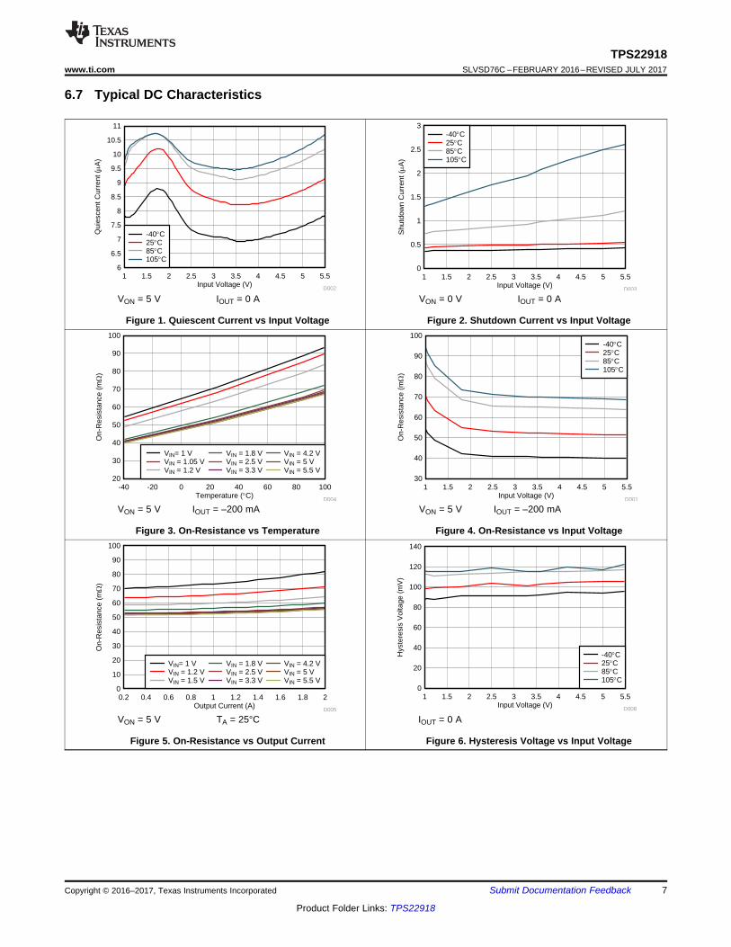
6.7 Typical DC Characteristics
VON = 5 V IOUT = 0 A
Figure 1. Quiescent Current vs Input Voltage
VON = 0 V IOUT = 0 A
Figure 2. Shutdown Current vs Input Voltage
VON = 5 V IOUT = –200 mA
Figure 3. On-Resistance vs Temperature
VON = 5 V IOUT = –200 mA
Figure 4. On-Resistance vs Input Voltage
VON = 5 V TA = 25°C
Figure 5. On-Resistance vs Output Current
IOUT = 0 A
Figure 6. Hysteresis Voltage vs Input Voltage

Input Voltage (V)
Out
put P
ull-D
own
Res
ista
nce
(:)
1 1.5 2 2.5 3 3.5 4 4.5 5 5.50
25
50
75
100
125
150
175
200
225
250
275
D009
-40qC25qC85qC105qC
8
TPS22918SLVSD76C –FEBRUARY 2016–REVISED JULY 2017 www.ti.com
Product Folder Links: TPS22918
Submit Documentation Feedback Copyright © 2016–2017, Texas Instruments Incorporated
Typical DC Characteristics (continued)
VIN = VOUT VON = 0 V
Figure 7. Output Pull-Down Resistance vs Input Voltage
Input Voltage (V)
Tur
non
Tim
e (P
s)
1 1.5 2 2.5 3 3.5 4 4.5 5 5.5650
950
1250
1550
1850
2150
D014
-40qC25qC85qC105qC
Input Voltage (V)
Fal
l Tim
e (P
s)
1 1.5 2 2.5 3 3.5 4 4.5 5 5.50
1
2
3
4
5
D012
-40qC25qC85qC105qC
Input Voltage (V)
Tur
noff
Tim
e (P
s)
1 1.5 2 2.5 3 3.5 4 4.5 5 5.50
1
2
3
4
5
D013
-40qC25qC85qC105qC
Input Voltage (V)
Ris
e T
ime
(Ps)
1 1.5 2 2.5 3 3.5 4 4.5 5 5.5500
1000
1500
2000
2500
3000
D010
-40qC25qC85qC105qC
Input Voltage (V)
Del
ay T
ime
(Ps)
1 1.5 2 2.5 3 3.5 4 4.5 5 5.5300
400
500
600
700
800
D011
-40qC25qC85qC105qC
9
TPS22918www.ti.com SLVSD76C –FEBRUARY 2016–REVISED JULY 2017
Product Folder Links: TPS22918
Submit Documentation FeedbackCopyright © 2016–2017, Texas Instruments Incorporated
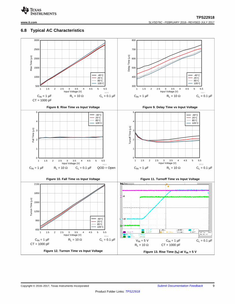
6.8 Typical AC Characteristics
CIN = 1 µF RL = 10 Ω CL = 0.1 µFCT = 1000 pF
Figure 8. Rise Time vs Input Voltage
CIN = 1 µF RL = 10 Ω CL = 0.1 µF
Figure 9. Delay Time vs Input Voltage
CIN = 1 µF RL = 10 Ω CL = 0.1 µF QOD = Open
Figure 10. Fall Time vs Input Voltage
CIN = 1 µF RL = 10 Ω CL = 0.1 µF
Figure 11. Turnoff Time vs Input Voltage
CIN = 1 µF RL = 10 Ω CL = 0.1 µFCT = 1000 pF
Figure 12. Turnon Time vs Input Voltage
VIN = 5 V CIN = 1 µF CL = 0.1 µFRL = 10 Ω CT = 1000 pF
Figure 13. Rise Time (tR) at VIN = 5 V

10
TPS22918SLVSD76C –FEBRUARY 2016–REVISED JULY 2017 www.ti.com
Product Folder Links: TPS22918
Submit Documentation Feedback Copyright © 2016–2017, Texas Instruments Incorporated
Typical AC Characteristics (continued)
VIN = 5 V CIN = 1 µF CL = 0.1 µFRL = 10 Ω QOD = Open
Figure 14. Fall Time (tF) at VIN = 5 V
VIN = 3.3 V CIN = 1 µF CL = 0.1 µFRL = 10 Ω CT = 1000 pF
Figure 15. Rise Time (tR) at VIN = 3.3 V
VIN = 3.3 V CIN = 1 µF CL = 0.1 µFRL = 10 Ω QOD = Open
Figure 16. Fall Time (tF) at VIN = 3.3 V
VIN = 1.8 V CIN = 1 µF CL = 0.1 µFRL = 10 Ω CT = 1000 pF
Figure 17. Rise Time (tR) at VIN = 1.8 V
VIN = 1.8 V CIN = 1 µF CL = 0.1 µFRL = 10 Ω QOD = Open
Figure 18. Fall Time (tF) at VIN = 1.8 V
VIN = 1.0 V CIN = 1 µF CL = 0.1 µFRL = 10 Ω CT = 1000 pF
Figure 19. Rise Time (tR) at VIN = 1 V

tRtON
tOFF
90% 90%
10% 10%
VON
VOUT
VOUT
50% 50%
50% 50%
tD
10%
tF
11
TPS22918www.ti.com SLVSD76C –FEBRUARY 2016–REVISED JULY 2017
Product Folder Links: TPS22918
Submit Documentation FeedbackCopyright © 2016–2017, Texas Instruments Incorporated
Typical AC Characteristics (continued)
VIN = 1.0 V CIN = 1 µF CL = 0.1 µFRL = 10 Ω QOD = Open
Figure 20. Fall Time (tF) at VIN = 1 V
7 Parameter Measurement Information
(1) Rise and fall times of the control signal are 100 ns(2) Turn-off times and fall times are dependent on the time constant at the load. For TPS22918, the internal pull-down
resistance RPD is enabled when the switch is disabled. The time constant is (RQOD || RL) × CL.
Figure 21. Test Circuit
Figure 22. Timing Waveforms

Control Logic
VIN
ON
VOUT
GND
Charge Pump
QOD
CT
Copyright © 2016, Texas Instruments Incorporated
12
TPS22918SLVSD76C –FEBRUARY 2016–REVISED JULY 2017 www.ti.com
Product Folder Links: TPS22918
Submit Documentation Feedback Copyright © 2016–2017, Texas Instruments Incorporated
8 Detailed Description
8.1 OverviewThe TPS22918 is a 5.5-V, 2-A load switch in a 6-pin SOT-23 package. To reduce voltage drop for low voltageand high current rails, the device implements a low resistance N-channel MOSFET which reduces the drop outvoltage across the device.
The device has a configurable slew rate which helps reduce or eliminate power supply droop because of largeinrush currents. Furthermore, the device features a QOD pin, which allows the configuration of the discharge rateof VOUT once the switch is disabled. During shutdown, the device has very low leakage currents, therebyreducing unnecessary leakages for downstream modules during standby. Integrated control logic, driver, chargepump, and output discharge FET eliminates the need for any external components which reduces solution sizeand bill of materials (BOM) count.
8.2 Functional Block Diagram

13
TPS22918www.ti.com SLVSD76C –FEBRUARY 2016–REVISED JULY 2017
Product Folder Links: TPS22918
Submit Documentation FeedbackCopyright © 2016–2017, Texas Instruments Incorporated
(1) TYPICAL VALUES WITH QOD SHORTED TO VOUT
8.3 Feature Description
8.3.1 On and Off ControlThe ON pin controls the state of the switch. ON is active high and has a low threshold, making it capable ofinterfacing with low-voltage signals. The ON pin is compatible with standard GPIO logic threshold. It can be usedwith any microcontroller with 1 V or higher GPIO voltage. This pin cannot be left floating and must be driveneither high or low for proper functionality.
8.3.2 Quick Output Discharge (QOD)The TPS22918 includes a QOD feature. The QOD pin can be configured in one of three ways:• QOD pin shorted to VOUT pin. Using this method, the discharge rate after the switch becomes disabled is
controlled with the value of the internal resistance RPD. The value of this resistance is listed in the ElectricalCharacteristics table.
• QOD pin connected to VOUT pin using an external resistor REXT. After the switch becomes disabled, thedischarge rate is controlled by the value of the total resistance of the QOD. To adjust the total QODresistance, Equation 1 can be used:
RQOD = RPD + REXT
Where:• RQOD = Total output discharge resistance• RPD = Internal pulldown resistance• REXT = External resistance placed between the VOUT and QOD pin. (1)
• QOD pin is unused and left floating. Using this method, there will be no quick output discharge functionality,and the output will remain floating after the switch is disabled.
The fall times of the device depend on many factors including the total resistance of the QOD, VIN, and theoutput capacitance. When QOD is shorted to VOUT, the fall time will change over VIN as the internal RPD variesover VIN. To calculate the approximate fall time of VOUT for a given RQOD, use Equation 2 and Table 1.
VCAP = VIN × e-t/τ
Where:• VCAP = Voltage across the capacitor (V)• t = Time since power supply removal (s)• τ = Time constant equal to RQOD × CL (2)
The fall times' dependency on VIN becomes minimal as the QOD value increases with additional externalresistance. See Table 1 for QOD fall times.
Table 1. QOD Fall Times
VIN (V)
(1)FALL TIME (μs) 90% - 10%, CIN = 1 μF, IOUT = 0 A , VON = 0 VTA = 25°C TA = 85°C
CL = 1 μF CL = 10 μF CL = 100 μF CL = 1 μF CL = 10 μF CL = 100 μF5.5 42 190 1880 40 210 21505 43 200 1905 45 220 2200
3.3 47 230 2150 50 260 25152.5 58 300 2790 60 345 32901.8 75 430 4165 80 490 49501.2 135 955 9910 135 1035 109801 230 1830 19625 210 1800 19270
14
TPS22918SLVSD76C –FEBRUARY 2016–REVISED JULY 2017 www.ti.com
Product Folder Links: TPS22918
Submit Documentation Feedback Copyright © 2016–2017, Texas Instruments Incorporated
8.3.2.1 QOD when System Power is RemovedThe adjustable QOD can be used to control the power down sequencing of a system even when the systempower supply is removed. When the power is removed, the input capacitor discharges at VIN. Past a certain VINlevel, the strength of the RPD will be reduced. If there is still remaining charge on the output capacitor, this willresult in longer fall times. For further information regarding this condition, see the Shutdown Sequencing DuringUnexpected System Power Loss section.
8.3.2.2 Internal QOD ConsiderationsSpecial considerations must be taken when using the internal RPD by shorting the QOD pin to the VOUT pin. Theinternal RPD is a pulldown resistance designed to quickly discharge a load after the switch has been disabled.Care must be used to ensure that excessive current does not flow through RPD during discharge so that themaximum TJ of 125°C is not exceeded. When using only the internal RPD to discharge a load, the total capacitiveload must not exceed 200 µF. Otherwise, an external resistor, REXT, must be used to ensure the amount ofcurrent flowing through RPD is properly limited and the maximum TJ is not exceeded. To ensure the device is notdamaged, the remaining charge from CL must decay naturally through the internal QOD resistance and shouldnot be driven.
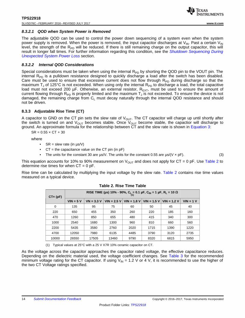
8.3.3 Adjustable Rise Time (CT)A capacitor to GND on the CT pin sets the slew rate of VOUT. The CT capacitor will charge up until shortly afterthe switch is turned on and VOUT becomes stable. Once VOUT become stable, the capactior will discharge toground. An approximate formula for the relationship between CT and the slew rate is shown in Equation 3:
SR = 0.55 × CT + 30
where• SR = slew rate (in µs/V)• CT = the capacitance value on the CT pin (in pF)• The units for the constant 30 are µs/V. The units for the constant 0.55 are µs/(V × pF). (3)
This equation accounts for 10% to 90% measurement on VOUT and does not apply for CT = 0 pF. Use Table 2 todetermine rise times for when CT = 0 pF.
Rise time can be calculated by multiplying the input voltage by the slew rate. Table 2 contains rise time valuesmeasured on a typical device.
(1) Typical values at 25°C with a 25 V X7R 10% ceramic capacitor on CT.
Table 2. Rise Time Table
CT× (pF)RISE TIME (µs) 10% - 90%, CL = 0.1 µF, CIN = 1 µF, RL = 10 Ω
(1)
VIN = 5 V VN = 3.3 V VIN = 2.5 V VIN = 1.8 V VIN = 1.5 V VIN = 1.2 V VIN = 1 V0 135 95 75 60 50 45 40
220 650 455 350 260 220 185 160470 1260 850 655 480 415 340 3001000 2540 1680 1300 960 810 660 5602200 5435 3580 2760 2020 1715 1390 12204700 12050 7980 6135 4485 3790 3120 2735
10000 26550 17505 13460 9790 8320 6815 5950
As the voltage across the capacitor approaches the capacitor rated voltage, the effective capacitance reduces.Depending on the dielectric material used, the voltage coefficient changes. See Table 3 for the recommendedminimum voltage rating for the CT capacitor. If using VIN = 1.2 V or 4 V, it is recommended to use the higher ofthe two CT Voltage ratings specified.
15
TPS22918www.ti.com SLVSD76C –FEBRUARY 2016–REVISED JULY 2017
Product Folder Links: TPS22918
Submit Documentation FeedbackCopyright © 2016–2017, Texas Instruments Incorporated
Table 3. Recommended CT Capacitor Voltage Rating
VIN (V) RECOMMENDED CT CAPACITOR VOLTAGERATING (V)
1 V to 1.2 V 101.2 V to 4 V 164 V to 5.5 V 20
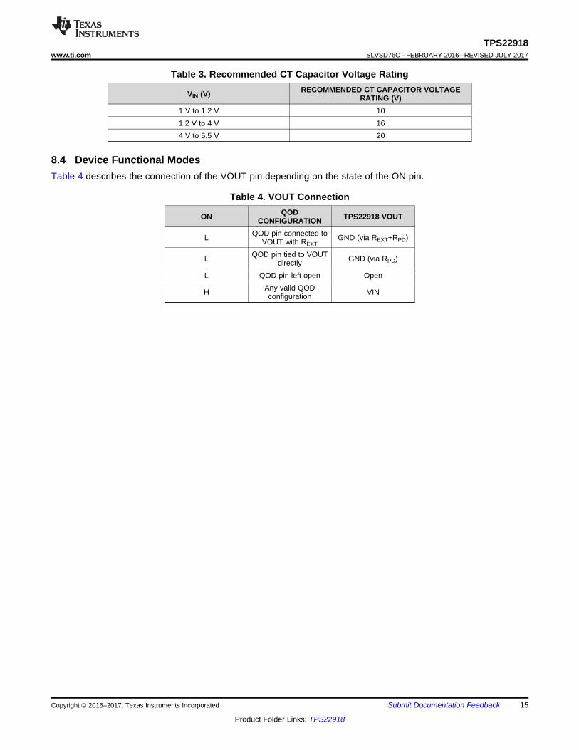
8.4 Device Functional ModesTable 4 describes the connection of the VOUT pin depending on the state of the ON pin.
Table 4. VOUT Connection
ON QODCONFIGURATION TPS22918 VOUT
L QOD pin connected toVOUT with REXT
GND (via REXT+RPD)
L QOD pin tied to VOUTdirectly GND (via RPD)
L QOD pin left open Open
H Any valid QODconfiguration VIN

16
TPS22918SLVSD76C –FEBRUARY 2016–REVISED JULY 2017 www.ti.com
Product Folder Links: TPS22918
Submit Documentation Feedback Copyright © 2016–2017, Texas Instruments Incorporated
9 Application and Implementation
NOTEInformation in the following applications sections is not part of the TI componentspecification, and TI does not warrant its accuracy or completeness. TI’s customers areresponsible for determining suitability of components for their purposes. Customers shouldvalidate and test their design implementation to confirm system functionality.
9.1 Application InformationThis section highlights some of the design considerations when implementing this device in various applications.A PSPICE model for this device is also available in the product page of this device on www.ti.com (See theDevice Support section for more information).
9.2 Typical ApplicationThis typical application demonstrates how the TPS22918 can be used to power downstream modules.
Figure 23. Typical Application Schematic
9.2.1 Design RequirementsFor this design example, use the values listed in Table 5 as the design parameters:
Table 5. Design ParametersDESIGN PARAMETER EXAMPLE VALUE
VIN 5 VLoad Current 2 A
CL 22 µFDesired Fall Time 4 ms
Maximum Acceptable Inrush Current 400 mA

17
TPS22918www.ti.com SLVSD76C –FEBRUARY 2016–REVISED JULY 2017
Product Folder Links: TPS22918
Submit Documentation FeedbackCopyright © 2016–2017, Texas Instruments Incorporated
9.2.2 Detailed Design Procedure
9.2.2.1 Input Capacitor (CIN)To limit the voltage drop on the input supply caused by transient in-rush currents when the switch turns on into adischarged load capacitor or short-circuit, a capacitor needs to be placed between VIN and GND. A 1 µF ceramiccapacitor, CIN, placed close to the pins, is usually sufficient. Higher values of CIN can be used to further reducethe voltage drop during high-current application. When switching heavy loads, it is recommended to have aninput capacitor about 10 times higher than the output capacitor to avoid excessive voltage drop.
9.2.2.2 Output Capacitor (CL) (Optional)Becuase of the integrated body diode in the MOSFET, a CIN greater than CL is highly recommended. A CLgreater than CIN can cause VOUT to exceed VIN when the system supply is removed. This could result in currentflow through the body diode from VOUT to VIN. A CIN to CL ratio of 10 to 1 is recommended for minimizing VINdip caused by inrush currents during startup.
9.2.2.3 Shutdown Sequencing During Unexpected System Power LossMicrocontrollers and processors often have a specific shutdown sequence in which power needs to be removed.Using the adjustable Quick Output Discharge function of the TPS22918, adding a load switch to each power railcan be used to manage the power down sequencing in the event of an unexpected system power loss (i.e.battery removal). To determine the QOD values for each load switch, first confirm the power down order of thedevice you wish to power sequence. Be sure to check if there are voltage or timing margins that must bemaintained during power down. Next, consult QOD Fall Time Table in the Quick Output Discharge (QOD) featuredescription to determine appropriate COUT and RQOD values for each power rail's load switch so that the loadswitches' fall times correspond to the order in which they need to be powered down. In the above example, wewould like this power rail's fall time to be 4 ms. Using Equation 2, to determine the appropriate RQOD to achieveour desired fall time.Because fall times are measured from 90% of VOUT to 10% of VOUT, the equation becomes:
.5 V = 4.5 V × e-(4 ms) / (R × (22 µF)) (4)RQOD = 83.333 Ω (5)
Refer to Figure 7, RPD at VIN = 5 V is approximately 25 Ω. Using Equation 1, the required external QODresistance can be calculated:
83.333 Ω = 25 Ω + REXT (6)REXT = 58.333 Ω (7)
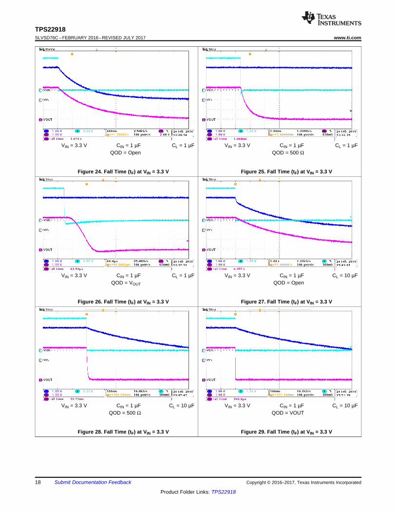
Figure 24 through Figure 29 are scope shots demonstrating an example of the QOD functionality when power isremoved from the device (both ON and VIN are disconnected simultaneously). The input voltage is decaying inall scope shots below.• Initial VIN = 3.3 V• QOD = Open, 500 Ω, or shorted to VOUT• CL = 1 μF, 10 μF• VOUT is left floatingNOTE: VIN may appear constant in some figures. This is because the time scale of the scope shot is too small toshow the decay of CIN.
18
TPS22918SLVSD76C –FEBRUARY 2016–REVISED JULY 2017 www.ti.com
Product Folder Links: TPS22918
Submit Documentation Feedback Copyright © 2016–2017, Texas Instruments Incorporated
VIN = 3.3 V CIN = 1 µF CL = 1 µFQOD = Open
Figure 24. Fall Time (tF) at VIN = 3.3 V
VIN = 3.3 V CIN = 1 µF CL = 1 µFQOD = 500 Ω
Figure 25. Fall Time (tF) at VIN = 3.3 V
VIN = 3.3 V CIN = 1 µF CL = 1 µFQOD = VOUT
Figure 26. Fall Time (tF) at VIN = 3.3 V
VIN = 3.3 V CIN = 1 µF CL = 10 µFQOD = Open
Figure 27. Fall Time (tF) at VIN = 3.3 V
VIN = 3.3 V CIN = 1 µF CL = 10 µFQOD = 500 Ω
Figure 28. Fall Time (tF) at VIN = 3.3 V
VIN = 3.3 V CIN = 1 µF CL = 10 µFQOD = VOUT
Figure 29. Fall Time (tF) at VIN = 3.3 V
OUTINRUSH L
dVI C
dt= ´
19
TPS22918www.ti.com SLVSD76C –FEBRUARY 2016–REVISED JULY 2017
Product Folder Links: TPS22918
Submit Documentation FeedbackCopyright © 2016–2017, Texas Instruments Incorporated
9.2.2.4 VIN to VOUT Voltage DropThe VIN to VOUT voltage drop in the device is determined by the RON of the device and the load current. TheRON of the device depends upon the VIN conditions of the device. Refer to the RON specification of the device inthe Electrical Characteristics table of this data sheet. When the RON of the device is determined based upon theVIN conditions, use Equation 8 to calculate the VIN to VOUT voltage drop:
∆V = ILOAD × RON
where• ΔV = voltage drop from VIN to VOUT• ILOAD = load current• RON = On-resistance of the device for a specific VIN
An appropriate ILOAD must be chosen such that the IMAX specification of the device is not violated. (8)
9.2.2.5 Inrush CurrentUse Equation 9 to determine how much inrush current will be caused by the CL capacitor:
where• IINRUSH = amount of inrush caused by CL
• CL = capacitance on VOUT• dt = Output Voltage rise time during the ramp up of VOUT when the device is enabled• dVOUT = change in VOUT during the ramp up of VOUT when the device is enabled (9)
The appropriate rise time can be calculated using the design requirements and the inrush current equation. Aswe are calculating the rise time (measured from 10% to 90% of VOUT), we will account for this in our dVOUTparameter (80% of VOUT = 4 V).
400 mA = 22 pF × 4 V/dt (10)dt = 220 μs (11)
To ensure an inrush current of less than 400 mA, choose a CT value that will yield a rise time of more than 220μs. Consulting Table 2 at VIN = 5 V, CT = 220 pF will provide a typical rise time of 650 μs. Inputting this rise timeand voltage into Equation 9, yields:
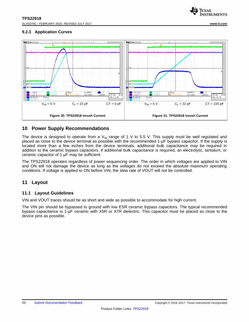
IInrush = 22 pF × 4 V / 650 μs (12)IInrush = 135 mA (13)
This inrush current can be seen in the Application Curves section. An appropriate CL value should be placed onVOUT such that the IMAX and IPLS specifications of the device are not violated.
20
TPS22918SLVSD76C –FEBRUARY 2016–REVISED JULY 2017 www.ti.com
Product Folder Links: TPS22918
Submit Documentation Feedback Copyright © 2016–2017, Texas Instruments Incorporated
9.2.3 Application Curves
VIN = 5 V CL = 22 pF CT = 0 pF
Figure 30. TPS22918 Inrush Current
VIN = 5 V CL = 22 pF CT = 220 pF
Figure 31. TPS22918 Inrush Current
10 Power Supply RecommendationsThe device is designed to operate from a VIN range of 1 V to 5.5 V. This supply must be well regulated andplaced as close to the device terminal as possible with the recommended 1-µF bypass capacitor. If the supply islocated more than a few inches from the device terminals, additional bulk capacitance may be required inaddition to the ceramic bypass capacitors. If additional bulk capacitance is required, an electrolytic, tantalum, orceramic capacitor of 1 µF may be sufficient.
The TPS22918 operates regardless of power sequencing order. The order in which voltages are applied to VINand ON will not damage the device as long as the voltages do not exceed the absolute maximum operatingconditions. If voltage is applied to ON before VIN, the slew rate of VOUT will not be controlled.
11 Layout
11.1 Layout GuidelinesVIN and VOUT traces should be as short and wide as possible to accommodate for high current.
The VIN pin should be bypassed to ground with low ESR ceramic bypass capacitors. The typical recommendedbypass capacitance is 1-µF ceramic with X5R or X7R dielectric. This capacitor must be placed as close to thedevice pins as possible.

J(MAX) AD(MAX)
JA
T TP
-=
q
1 VOUT
2 QOD
3 CT 4ON
5GND
6VIN
VIA to Power Ground Plane
21
TPS22918www.ti.com SLVSD76C –FEBRUARY 2016–REVISED JULY 2017
Product Folder Links: TPS22918
Submit Documentation FeedbackCopyright © 2016–2017, Texas Instruments Incorporated
11.2 Layout Example
Figure 32. Recommended Board Layout
11.3 Thermal ConsiderationsFor best performance, all traces must be as short as possible. To be most effective, the input and outputcapacitors must be placed close to the device to minimize the effects that parasitic trace inductances may haveon normal and short-circuit operation. Using wide traces for VIN, VOUT, and GND helps minimize the parasiticelectrical effects along with minimizing the case to ambient thermal impedance.
The maximum IC junction temperature should be restricted to 125°C under normal operating conditions. Tocalculate the maximum allowable dissipation, PD(max) for a given output current and ambient temperature, useEquation 14:
where• PD(MAX) = maximum allowable power dissipation• TJ(MAX) = maximum allowable junction temperature (125°C for the TPS22918)• TA = ambient temperature of the device• θJA = junction to air thermal impedance. Refer to the Thermal Information table. This parameter is highly
dependent upon board layout. (14)

22
TPS22918SLVSD76C –FEBRUARY 2016–REVISED JULY 2017 www.ti.com
Product Folder Links: TPS22918
Submit Documentation Feedback Copyright © 2016–2017, Texas Instruments Incorporated
12 Device and Documentation Support
12.1 Device Support
12.1.1 Developmental SupportFor the TPS22918 PSpice Transient Model, see SLVMBI6.
12.2 Documentation Support
12.2.1 Related DocumentationFor related documentation see the following:
TPS22918 5.5-V, 2-A, 50-mΩ On-Resistance Load Switch Evaluation Module, SLVUAP0.
12.3 Community ResourcesThe following links connect to TI community resources. Linked contents are provided "AS IS" by the respectivecontributors. They do not constitute TI specifications and do not necessarily reflect TI's views; see TI's Terms ofUse.
TI E2E™ Online Community TI's Engineer-to-Engineer (E2E) Community. Created to foster collaborationamong engineers. At e2e.ti.com, you can ask questions, share knowledge, explore ideas and helpsolve problems with fellow engineers.
Design Support TI's Design Support Quickly find helpful E2E forums along with design support tools andcontact information for technical support.
12.4 TrademarksE2E is a trademark of Texas Instruments.All other trademarks are the property of their respective owners.
12.5 Electrostatic Discharge CautionThese devices have limited built-in ESD protection. The leads should be shorted together or the device placed in conductive foamduring storage or handling to prevent electrostatic damage to the MOS gates.
12.6 GlossarySLYZ022 — TI Glossary.
This glossary lists and explains terms, acronyms, and definitions.
13 Mechanical, Packaging, and Orderable InformationThe following pages include mechanical, packaging, and orderable information. This information is the mostcurrent data available for the designated devices. This data is subject to change without notice and revision ofthis document. For browser-based versions of this data sheet, refer to the left-hand navigation.
PACKAGE OPTION ADDENDUM
www.ti.com 14-Jun-2017
Addendum-Page 1
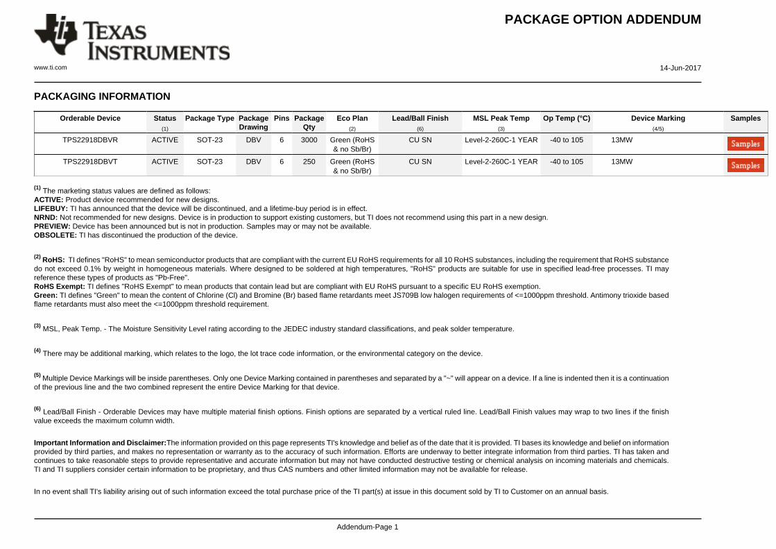
PACKAGING INFORMATION
Orderable Device Status(1)
Package Type PackageDrawing
Pins PackageQty
Eco Plan(2)
Lead/Ball Finish(6)
MSL Peak Temp(3)
Op Temp (°C) Device Marking(4/5)
Samples
TPS22918DBVR ACTIVE SOT-23 DBV 6 3000 Green (RoHS& no Sb/Br)
CU SN Level-2-260C-1 YEAR -40 to 105 13MW
TPS22918DBVT ACTIVE SOT-23 DBV 6 250 Green (RoHS& no Sb/Br)
CU SN Level-2-260C-1 YEAR -40 to 105 13MW
(1) The marketing status values are defined as follows:ACTIVE: Product device recommended for new designs.LIFEBUY: TI has announced that the device will be discontinued, and a lifetime-buy period is in effect.NRND: Not recommended for new designs. Device is in production to support existing customers, but TI does not recommend using this part in a new design.PREVIEW: Device has been announced but is not in production. Samples may or may not be available.OBSOLETE: TI has discontinued the production of the device.
(2) RoHS: TI defines "RoHS" to mean semiconductor products that are compliant with the current EU RoHS requirements for all 10 RoHS substances, including the requirement that RoHS substancedo not exceed 0.1% by weight in homogeneous materials. Where designed to be soldered at high temperatures, "RoHS" products are suitable for use in specified lead-free processes. TI mayreference these types of products as "Pb-Free".RoHS Exempt: TI defines "RoHS Exempt" to mean products that contain lead but are compliant with EU RoHS pursuant to a specific EU RoHS exemption.Green: TI defines "Green" to mean the content of Chlorine (Cl) and Bromine (Br) based flame retardants meet JS709B low halogen requirements of <=1000ppm threshold. Antimony trioxide basedflame retardants must also meet the <=1000ppm threshold requirement.
(3) MSL, Peak Temp. - The Moisture Sensitivity Level rating according to the JEDEC industry standard classifications, and peak solder temperature.
(4) There may be additional marking, which relates to the logo, the lot trace code information, or the environmental category on the device.
(5) Multiple Device Markings will be inside parentheses. Only one Device Marking contained in parentheses and separated by a "~" will appear on a device. If a line is indented then it is a continuationof the previous line and the two combined represent the entire Device Marking for that device.
(6) Lead/Ball Finish - Orderable Devices may have multiple material finish options. Finish options are separated by a vertical ruled line. Lead/Ball Finish values may wrap to two lines if the finishvalue exceeds the maximum column width.
Important Information and Disclaimer:The information provided on this page represents TI's knowledge and belief as of the date that it is provided. TI bases its knowledge and belief on informationprovided by third parties, and makes no representation or warranty as to the accuracy of such information. Efforts are underway to better integrate information from third parties. TI has taken andcontinues to take reasonable steps to provide representative and accurate information but may not have conducted destructive testing or chemical analysis on incoming materials and chemicals.TI and TI suppliers consider certain information to be proprietary, and thus CAS numbers and other limited information may not be available for release.
In no event shall TI's liability arising out of such information exceed the total purchase price of the TI part(s) at issue in this document sold by TI to Customer on an annual basis.

PACKAGE OPTION ADDENDUM
www.ti.com 14-Jun-2017
Addendum-Page 2
OTHER QUALIFIED VERSIONS OF TPS22918 :
• Automotive: TPS22918-Q1
NOTE: Qualified Version Definitions:
• Automotive - Q100 devices qualified for high-reliability automotive applications targeting zero defects
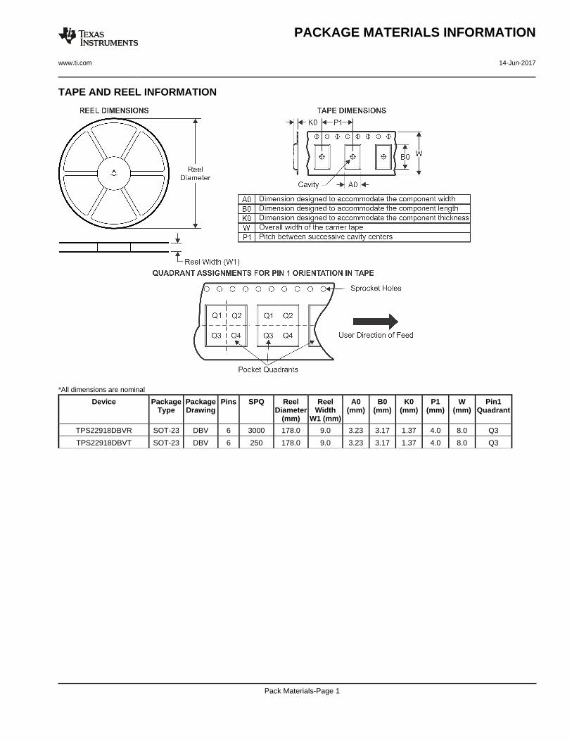
TAPE AND REEL INFORMATION
*All dimensions are nominal
Device PackageType
PackageDrawing
Pins SPQ ReelDiameter
(mm)
ReelWidth
W1 (mm)
A0(mm)
B0(mm)
K0(mm)
P1(mm)
W(mm)
Pin1Quadrant
TPS22918DBVR SOT-23 DBV 6 3000 178.0 9.0 3.23 3.17 1.37 4.0 8.0 Q3
TPS22918DBVT SOT-23 DBV 6 250 178.0 9.0 3.23 3.17 1.37 4.0 8.0 Q3
PACKAGE MATERIALS INFORMATION
www.ti.com 14-Jun-2017
Pack Materials-Page 1

*All dimensions are nominal
Device Package Type Package Drawing Pins SPQ Length (mm) Width (mm) Height (mm)
TPS22918DBVR SOT-23 DBV 6 3000 190.0 190.0 30.0
TPS22918DBVT SOT-23 DBV 6 250 190.0 190.0 30.0
PACKAGE MATERIALS INFORMATION
www.ti.com 14-Jun-2017
Pack Materials-Page 2


IMPORTANT NOTICE
Texas Instruments Incorporated (TI) reserves the right to make corrections, enhancements, improvements and other changes to itssemiconductor products and services per JESD46, latest issue, and to discontinue any product or service per JESD48, latest issue. Buyersshould obtain the latest relevant information before placing orders and should verify that such information is current and complete.TI’s published terms of sale for semiconductor products (http://www.ti.com/sc/docs/stdterms.htm) apply to the sale of packaged integratedcircuit products that TI has qualified and released to market. Additional terms may apply to the use or sale of other types of TI products andservices.Reproduction of significant portions of TI information in TI data sheets is permissible only if reproduction is without alteration and isaccompanied by all associated warranties, conditions, limitations, and notices. TI is not responsible or liable for such reproduceddocumentation. Information of third parties may be subject to additional restrictions. Resale of TI products or services with statementsdifferent from or beyond the parameters stated by TI for that product or service voids all express and any implied warranties for theassociated TI product or service and is an unfair and deceptive business practice. TI is not responsible or liable for any such statements.Buyers and others who are developing systems that incorporate TI products (collectively, “Designers”) understand and agree that Designersremain responsible for using their independent analysis, evaluation and judgment in designing their applications and that Designers havefull and exclusive responsibility to assure the safety of Designers' applications and compliance of their applications (and of all TI productsused in or for Designers’ applications) with all applicable regulations, laws and other applicable requirements. Designer represents that, withrespect to their applications, Designer has all the necessary expertise to create and implement safeguards that (1) anticipate dangerousconsequences of failures, (2) monitor failures and their consequences, and (3) lessen the likelihood of failures that might cause harm andtake appropriate actions. Designer agrees that prior to using or distributing any applications that include TI products, Designer willthoroughly test such applications and the functionality of such TI products as used in such applications.TI’s provision of technical, application or other design advice, quality characterization, reliability data or other services or information,including, but not limited to, reference designs and materials relating to evaluation modules, (collectively, “TI Resources”) are intended toassist designers who are developing applications that incorporate TI products; by downloading, accessing or using TI Resources in anyway, Designer (individually or, if Designer is acting on behalf of a company, Designer’s company) agrees to use any particular TI Resourcesolely for this purpose and subject to the terms of this Notice.TI’s provision of TI Resources does not expand or otherwise alter TI’s applicable published warranties or warranty disclaimers for TIproducts, and no additional obligations or liabilities arise from TI providing such TI Resources. TI reserves the right to make corrections,enhancements, improvements and other changes to its TI Resources. TI has not conducted any testing other than that specificallydescribed in the published documentation for a particular TI Resource.Designer is authorized to use, copy and modify any individual TI Resource only in connection with the development of applications thatinclude the TI product(s) identified in such TI Resource. NO OTHER LICENSE, EXPRESS OR IMPLIED, BY ESTOPPEL OR OTHERWISETO ANY OTHER TI INTELLECTUAL PROPERTY RIGHT, AND NO LICENSE TO ANY TECHNOLOGY OR INTELLECTUAL PROPERTYRIGHT OF TI OR ANY THIRD PARTY IS GRANTED HEREIN, including but not limited to any patent right, copyright, mask work right, orother intellectual property right relating to any combination, machine, or process in which TI products or services are used. Informationregarding or referencing third-party products or services does not constitute a license to use such products or services, or a warranty orendorsement thereof. Use of TI Resources may require a license from a third party under the patents or other intellectual property of thethird party, or a license from TI under the patents or other intellectual property of TI.TI RESOURCES ARE PROVIDED “AS IS” AND WITH ALL FAULTS. TI DISCLAIMS ALL OTHER WARRANTIES ORREPRESENTATIONS, EXPRESS OR IMPLIED, REGARDING RESOURCES OR USE THEREOF, INCLUDING BUT NOT LIMITED TOACCURACY OR COMPLETENESS, TITLE, ANY EPIDEMIC FAILURE WARRANTY AND ANY IMPLIED WARRANTIES OFMERCHANTABILITY, FITNESS FOR A PARTICULAR PURPOSE, AND NON-INFRINGEMENT OF ANY THIRD PARTY INTELLECTUALPROPERTY RIGHTS. TI SHALL NOT BE LIABLE FOR AND SHALL NOT DEFEND OR INDEMNIFY DESIGNER AGAINST ANY CLAIM,INCLUDING BUT NOT LIMITED TO ANY INFRINGEMENT CLAIM THAT RELATES TO OR IS BASED ON ANY COMBINATION OFPRODUCTS EVEN IF DESCRIBED IN TI RESOURCES OR OTHERWISE. IN NO EVENT SHALL TI BE LIABLE FOR ANY ACTUAL,DIRECT, SPECIAL, COLLATERAL, INDIRECT, PUNITIVE, INCIDENTAL, CONSEQUENTIAL OR EXEMPLARY DAMAGES INCONNECTION WITH OR ARISING OUT OF TI RESOURCES OR USE THEREOF, AND REGARDLESS OF WHETHER TI HAS BEENADVISED OF THE POSSIBILITY OF SUCH DAMAGES.Unless TI has explicitly designated an individual product as meeting the requirements of a particular industry standard (e.g., ISO/TS 16949and ISO 26262), TI is not responsible for any failure to meet such industry standard requirements.Where TI specifically promotes products as facilitating functional safety or as compliant with industry functional safety standards, suchproducts are intended to help enable customers to design and create their own applications that meet applicable functional safety standardsand requirements. Using products in an application does not by itself establish any safety features in the application. Designers mustensure compliance with safety-related requirements and standards applicable to their applications. Designer may not use any TI products inlife-critical medical equipment unless authorized officers of the parties have executed a special contract specifically governing such use.Life-critical medical equipment is medical equipment where failure of such equipment would cause serious bodily injury or death (e.g., lifesupport, pacemakers, defibrillators, heart pumps, neurostimulators, and implantables). Such equipment includes, without limitation, allmedical devices identified by the U.S. Food and Drug Administration as Class III devices and equivalent classifications outside the U.S.TI may expressly designate certain products as completing a particular qualification (e.g., Q100, Military Grade, or Enhanced Product).Designers agree that it has the necessary expertise to select the product with the appropriate qualification designation for their applicationsand that proper product selection is at Designers’ own risk. Designers are solely responsible for compliance with all legal and regulatoryrequirements in connection with such selection.Designer will fully indemnify TI and its representatives against any damages, costs, losses, and/or liabilities arising out of Designer’s non-compliance with the terms and provisions of this Notice.
Mailing Address: Texas Instruments, Post Office Box 655303, Dallas, Texas 75265Copyright © 2017, Texas Instruments Incorporated