Embed Size (px)
Citation preview

Copyright © 2016, Texas Instruments Incorporated
Product
Folder
Sample &Buy
Technical
Documents
Tools &
Software
Support &Community
An IMPORTANT NOTICE at the end of this data sheet addresses availability, warranty, changes, use in safety-critical applications,intellectual property matters and other important disclaimers. PRODUCTION DATA.
TPS60130, TPS60131, TPS60132, TPS60133SLVS258B –NOVEMBER 1999–REVISED DECEMBER 2016
TPS6013x Regulated 5-V, 300-mA High-Efficiency Charge Pump DC-DC Converters
1
1 Features1• Up to 90% Efficiency From 2.7-V to 5.4-V Input
Voltage Range Because of Special SwitchingTopology
• Up to 300-mA Output Current (TPS60130 andTPS60131)
• No Inductors Required, Low EMI• Regulated 5-V ±4% Output• Only Four External Components Required• 60-µA Quiescent Supply Current• 0.05-µA Shutdown Current• Load Disconnected in Shutdown• Thermally-Enhanced PowerPAD™ Package
2 Applications• Battery-Powered Applications• Three Battery Cells to 5-V Conversion or Point-of-
Use 3.3-V to 5-V Conversion• Lilon Battery to 5-V Conversion• Portable Instruments• Battery-Powered Microprocessor Systems• Backup-Battery Boost Converters• PDA’s, Organizers, Laptops• Handheld Instrumentation• Medical Instruments (for example, Glucose
Meters)• PCMCIA and 5-V Smart Card Supply
3 DescriptionThe TPS6013x step-up, regulated charge pumpdevices generate a 5-V ±4% output voltage from a2.7-V to 5.4-V input voltage (three alkaline, NiCd, orNiMH batteries or one Lithium or Lilon battery). Theoutput current is 300 mA for the TPS60130 andTPS60131, and 150 mA for the TPS60132 andTPS60133 devices, all from a 3-V input. Only fourexternal capacitors are required to build a completehigh efficiency dc/dc charge pump converter. Toachieve the high efficiency over a wide input voltagerange, the charge pump automatically selectsbetween a 1.5× or doubler conversion mode. From a3-V input, all ICs can start with full load current.
Device Information(1)
PART NUMBER PACKAGE BODY SIZE (NOM)TPS6013x HTSSOP (20) 6.50 mm × 4.40 mm
(1) For all available packages, see the orderable addendum atthe end of the data sheet.
Typical Operating Circuit
2
TPS60130, TPS60131, TPS60132, TPS60133SLVS258B –NOVEMBER 1999–REVISED DECEMBER 2016 www.ti.com
Product Folder Links: TPS60130 TPS60131 TPS60132 TPS60133
Submit Documentation Feedback Copyright © 1999–2016, Texas Instruments Incorporated
Table of Contents1 Features .................................................................. 12 Applications ........................................................... 13 Description ............................................................. 14 Revision History..................................................... 25 Device Options....................................................... 36 Pin Configuration and Functions ......................... 47 Specifications......................................................... 5
7.1 Absolute Maximum Ratings ...................................... 57.2 ESD Ratings.............................................................. 57.3 Recommended Operating Conditions....................... 57.4 Thermal Information .................................................. 57.5 Electrical Characteristics........................................... 67.6 Dissipation Ratings ................................................... 67.7 Typical Characteristics .............................................. 7
8 Parameter Measurement Information ................ 119 Detailed Description ............................................ 12
9.1 Overview ................................................................. 129.2 Functional Block Diagram ....................................... 12
9.3 Feature Description................................................. 1310 Application and Implementation........................ 17
10.1 Application Information.......................................... 1710.2 Typical Applications .............................................. 17
11 Power Supply Recommendations ..................... 2212 Layout................................................................... 22
12.1 Layout Guidelines ................................................. 2212.2 Layout Example .................................................... 2212.3 Power Dissipation ................................................. 22
13 Device and Documentation Support ................. 2413.1 Documentation Support ........................................ 2413.2 Related Links ........................................................ 2413.3 Receiving Notification of Documentation Updates 2413.4 Community Resources.......................................... 2413.5 Trademarks ........................................................... 2413.6 Electrostatic Discharge Caution............................ 2413.7 Glossary ................................................................ 24
14 Mechanical, Packaging, and OrderableInformation ........................................................... 25
4 Revision HistoryNOTE: Page numbers for previous revisions may differ from page numbers in the current version.
Changes from Revision A (December 1999) to Revision B Page
• Added ESD Ratings table, Feature Description section, Device Functional Modes, Application and Implementationsection, Power Supply Recommendations section, Layout section, Device and Documentation Support section, andMechanical, Packaging, and Orderable Information section ................................................................................................. 1
• Deleted Lead temperature (260°C maximum) from Absolute Maximum Ratings table.......................................................... 5

3
TPS60130, TPS60131, TPS60132, TPS60133www.ti.com SLVS258B –NOVEMBER 1999–REVISED DECEMBER 2016
Product Folder Links: TPS60130 TPS60131 TPS60132 TPS60133
Submit Documentation FeedbackCopyright © 1999–2016, Texas Instruments Incorporated
5 Device Options
Table 1. Available OptionsPART NUMBER DEVICE FEATURES
TPS60130 Low battery detector3-cell to 5 V, 300 mA
TPS60131 Power good detectorTPS60132 Low battery detector
3-cell to 5 V, 150 mATPS60133 Power good detector
Table 2. Device Family ProductsPART NUMBER DESCRIPTION
TPS60100 Regulated 3.3-V, 200-mA low-noise charge pump dc-dc converterTPS60101 Regulated 3.3-V, 100-mA low-noise charge pump dc-dc converterTPS60110 Regulated 5-V, 300-mA low-noise charge pump dc-dc converterTPS60111 Regulated 5-V, 150-mA low-noise charge pump dc-dc converterTPS60120 Regulated 3.3-V, 200-mA high efficiency charge pump dc-dc converter with low battery comparatorTPS60121 Regulated 3.3-V, 200-mA high efficiency charge pump dc-dc converter with Power Good comparatorTPS60122 Regulated 3.3-V, 100-mA high efficiency charge pump dc-dc converter with low battery comparatorTPS60123 Regulated 3.3-V, 100-mA high efficiency charge pump dc-dc converter with Power Good comparator

4
TPS60130, TPS60131, TPS60132, TPS60133SLVS258B –NOVEMBER 1999–REVISED DECEMBER 2016 www.ti.com
Product Folder Links: TPS60130 TPS60131 TPS60132 TPS60133
Submit Documentation Feedback Copyright © 1999–2016, Texas Instruments Incorporated
6 Pin Configuration and Functions
TPS60130 and TPS60132 PWP Package20-Pin HTSSOP
Top ViewTPS60131 and TPS60133 PWP Package
20-Pin HTSSOPTop View
Pin FunctionsPIN
I/O DESCRIPTIONNAME NO.C1+ 6 — Positive pin of the flying capacitor C1C1– 8 — Negative pin of the flying capacitor C1C2+ 15 — Positive pin of the flying capacitor C2C2– 13 — Negative pin of the flying capacitor C2
ENABLE 3 IEnable input. Connect ENABLE to IN for normal operation. When ENABLE is a logic low, thedevice turns off and the supply current decreases to 0.05 µA. The output is disconnectedfrom the input when the device is disabled.
FB 4 I Feedback input. Connect FB to OUT as close to the load as possible to achieve bestregulation. A resistive divider is on the chip to match internal reference voltage of 1.21 V.
GND 1, 2, 19, 20 — Ground. Analog ground for internal reference and control circuitry. Connect to PGND pinsthrough a short trace.
IN 7, 14 I Supply input. Bypass IN to PGND with a capacitor that has half of the capacitance of theoutput capacitor. Connect both IN pins together through a short trace.
LBO/PG 17 O
Low battery detector output (TPS60130 and TPS60132) or Power Good output (TPS60131and TPS60133). Open drain output of the low battery or Power Good comparator. It can sink1 mA. TI recommends a 100-kΩ to 1-MΩ pullup resistor to OUT. Leave the pin unconnectedif the low battery or Power Good detector is not used.
LBI/NC 18 I
Low battery detector input (TPS60130 and TPS60132 only). The voltage at this input iscompared to the internal 1.21-V reference voltage. Connect this pin to ground if the lowbattery detection function is not used. On the TPS60131 and TPS60133, this pin is notconnected.
OUT 5, 16 O Regulated 5-V power output. Connect both OUT pins through a short trace and bypass OUTto GND with the output filter capacitor CO.
PGND 9, 10, 11, 12 — Power ground. Charge-pump current flows through this pin. Connect all PGND pins together.
5
TPS60130, TPS60131, TPS60132, TPS60133www.ti.com SLVS258B –NOVEMBER 1999–REVISED DECEMBER 2016
Product Folder Links: TPS60130 TPS60131 TPS60132 TPS60133
Submit Documentation FeedbackCopyright © 1999–2016, Texas Instruments Incorporated
(1) Stresses beyond those listed under Absolute Maximum Ratings may cause permanent damage to the device. These are stress ratingsonly, which do not imply functional operation of the device at these or any other conditions beyond those indicated under RecommendedOperating Conditions. Exposure to absolute-maximum-rated conditions for extended periods may affect device reliability.
7 Specifications
7.1 Absolute Maximum Ratingsover operating free-air temperature range (unless otherwise noted) (1)
MIN MAX UNITInput voltage, VI (IN, OUT, ENABLE, FB, LBI, LBO/PG) –0.3 5.5 V
Differential input voltage, VIDC1+, C2+ to GND –0.3 VO + 0.3
VC1−, C2− to GND –0.3 VI + 0.3
Continuous total power dissipation See Dissipation Ratings
Continuous output currentTPS60130 and TPS60131 400
mATPS60132 and TPS60133 200
Maximum junction temperature 150 °CStorage temperature, Tstg 150 °C
(1) JEDEC document JEP155 states that 500-V HBM allows safe manufacturing with a standard ESD control process.(2) JEDEC document JEP157 states that 250-V CDM allows safe manufacturing with a standard ESD control process.
7.2 ESD RatingsVALUE UNIT
V(ESD) Electrostatic dischargeHuman-body model (HBM), per ANSI/ESDA/JEDEC JS-001 (1) ±2000
VCharged-device model (CDM), per JEDEC specification JESD22-C101 (2) ±1000Machine model (MM) ±200
7.3 Recommended Operating Conditionsover operating free-air temperature range (unless otherwise noted)
MIN MAX UNITVI Input voltage 2.7 5.4 V
IO Output currentTPS60130 and TPS60131 300
mATPS60132 and TPS60133 150
TJ Operating junction temperature 125 °C
(1) For more information about traditional and new thermal metrics, see the Semiconductor and IC Package Thermal Metrics applicationreport.
7.4 Thermal Information
THERMAL METRIC (1)TPS6013x
UNITPWP (HTSSOP)20 PINS
RθJA Junction-to-ambient thermal resistance 178.75 °C/WRθJC(bot) Junction-to-case (bottom) thermal resistance 3.5 °C/W
6
TPS60130, TPS60131, TPS60132, TPS60133SLVS258B –NOVEMBER 1999–REVISED DECEMBER 2016 www.ti.com
Product Folder Links: TPS60130 TPS60131 TPS60132 TPS60133
Submit Documentation Feedback Copyright © 1999–2016, Texas Instruments Incorporated
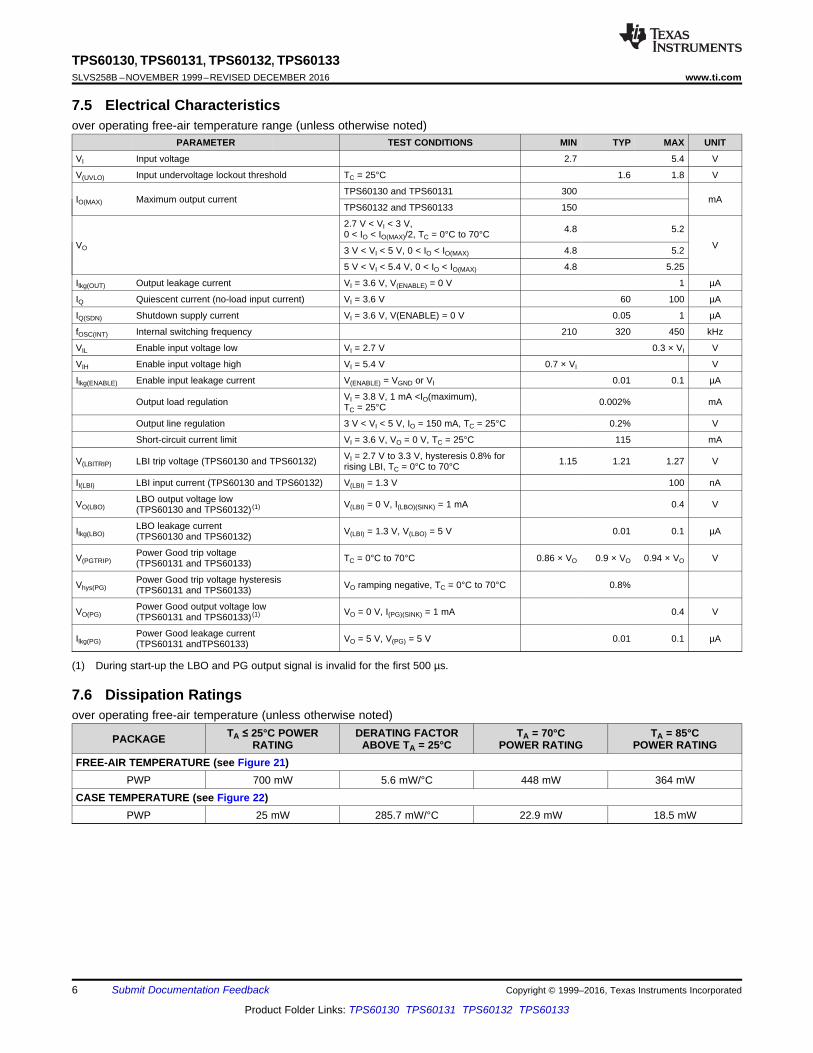
(1) During start-up the LBO and PG output signal is invalid for the first 500 µs.
7.5 Electrical Characteristicsover operating free-air temperature range (unless otherwise noted)
PARAMETER TEST CONDITIONS MIN TYP MAX UNIT
VI Input voltage 2.7 5.4 V
V(UVLO) Input undervoltage lockout threshold TC = 25°C 1.6 1.8 V
IO(MAX) Maximum output currentTPS60130 and TPS60131 300
mATPS60132 and TPS60133 150
VO
2.7 V < VI < 3 V,0 < IO < IO(MAX)/2, TC = 0°C to 70°C 4.8 5.2
V3 V < VI < 5 V, 0 < IO < IO(MAX) 4.8 5.2
5 V < VI < 5.4 V, 0 < IO < IO(MAX) 4.8 5.25
Ilkg(OUT) Output leakage current VI = 3.6 V, V(ENABLE) = 0 V 1 µA
IQ Quiescent current (no-load input current) VI = 3.6 V 60 100 µA
IQ(SDN) Shutdown supply current VI = 3.6 V, V(ENABLE) = 0 V 0.05 1 µA
fOSC(INT) Internal switching frequency 210 320 450 kHz
VIL Enable input voltage low VI = 2.7 V 0.3 × VI V
VIH Enable input voltage high VI = 5.4 V 0.7 × VI V
Ilkg(ENABLE) Enable input leakage current V(ENABLE) = VGND or VI 0.01 0.1 µA
Output load regulation VI = 3.8 V, 1 mA <IO(maximum),TC = 25°C 0.002% mA
Output line regulation 3 V < VI < 5 V, IO = 150 mA, TC = 25°C 0.2% V
Short-circuit current limit VI = 3.6 V, VO = 0 V, TC = 25°C 115 mA
V(LBITRIP) LBI trip voltage (TPS60130 and TPS60132) VI = 2.7 V to 3.3 V, hysteresis 0.8% forrising LBI, TC = 0°C to 70°C 1.15 1.21 1.27 V
II(LBI) LBI input current (TPS60130 and TPS60132) V(LBI) = 1.3 V 100 nA
VO(LBO)LBO output voltage low(TPS60130 and TPS60132) (1) V(LBI) = 0 V, I(LBO)(SINK) = 1 mA 0.4 V
Ilkg(LBO)LBO leakage current(TPS60130 and TPS60132) V(LBI) = 1.3 V, V(LBO) = 5 V 0.01 0.1 µA
V(PGTRIP)Power Good trip voltage(TPS60131 and TPS60133) TC = 0°C to 70°C 0.86 × VO 0.9 × VO 0.94 × VO V
Vhys(PG)Power Good trip voltage hysteresis(TPS60131 and TPS60133) VO ramping negative, TC = 0°C to 70°C 0.8%
VO(PG)Power Good output voltage low(TPS60131 and TPS60133) (1) VO = 0 V, I(PG)(SINK) = 1 mA 0.4 V
Ilkg(PG)Power Good leakage current(TPS60131 andTPS60133) VO = 5 V, V(PG) = 5 V 0.01 0.1 µA
7.6 Dissipation Ratingsover operating free-air temperature (unless otherwise noted)
PACKAGE TA ≤ 25°C POWERRATING
DERATING FACTORABOVE TA = 25°C
TA = 70°CPOWER RATING
TA = 85°CPOWER RATING
FREE-AIR TEMPERATURE (see Figure 21)PWP 700 mW 5.6 mW/°C 448 mW 364 mW
CASE TEMPERATURE (see Figure 22)PWP 25 mW 285.7 mW/°C 22.9 mW 18.5 mW

7
TPS60130, TPS60131, TPS60132, TPS60133www.ti.com SLVS258B –NOVEMBER 1999–REVISED DECEMBER 2016
Product Folder Links: TPS60130 TPS60131 TPS60132 TPS60133
Submit Documentation FeedbackCopyright © 1999–2016, Texas Instruments Incorporated
7.7 Typical CharacteristicsTable 3. Table of Graphs
FIGURE
η Efficiencyvs Output Current (TPS60130 and TPS60132) Figure 1, Figure 2vs Input Voltage (TPS60130 and TPS60132) Figure 3, Figure 4
I Supply Current vs Input Voltage Figure 5VO Output Voltage vs Output Current (TPS60130 and TPS60132) Figure 6, Figure 7VO Output Voltage Ripple vs Input Voltage (TPS60130 and TPS60132) Figure 8, Figure 9
VO Output Voltage Ripple Amplitude vs Time Figure 10, Figure 11,and Figure 12
VPP Output Voltage Ripple Amplitude vs Input Voltage Figure 13f(OSC) Oscillator Frequency vs Input Voltage Figure 14
Load Transient Response Figure 15Line Transient Response Figure 16
VO Output Voltage vs Time (Start-Up Timing) Figure 17

8
TPS60130, TPS60131, TPS60132, TPS60133SLVS258B –NOVEMBER 1999–REVISED DECEMBER 2016 www.ti.com
Product Folder Links: TPS60130 TPS60131 TPS60132 TPS60133
Submit Documentation Feedback Copyright © 1999–2016, Texas Instruments Incorporated
Figure 1. TPS60130 Efficiency vs Output Current Figure 2. TPS60132 Efficiency vs Output Current
Figure 3. TPS60130 Efficiency vs Input Voltage Figure 4. TPS60132 Efficiency vs Input Voltage
Figure 5. Supply Current vs Input Voltage Figure 6. TPS60132 Output Voltage vs Output Current

9
TPS60130, TPS60131, TPS60132, TPS60133www.ti.com SLVS258B –NOVEMBER 1999–REVISED DECEMBER 2016
Product Folder Links: TPS60130 TPS60131 TPS60132 TPS60133
Submit Documentation FeedbackCopyright © 1999–2016, Texas Instruments Incorporated
Figure 7. TPS60132 Output Voltage vs Output Current Figure 8. TPS60130 Output Voltage vs Input Voltage
Figure 9. TPS60132 Output Voltage vs Input Voltage Figure 10. Output Voltage Ripple vs Time
Figure 11. Output Voltage Ripple vs Time Figure 12. Output Voltage Ripple vs Time

10
TPS60130, TPS60131, TPS60132, TPS60133SLVS258B –NOVEMBER 1999–REVISED DECEMBER 2016 www.ti.com
Product Folder Links: TPS60130 TPS60131 TPS60132 TPS60133
Submit Documentation Feedback Copyright © 1999–2016, Texas Instruments Incorporated
Figure 13. Output Voltage Ripple Amplitudevs Input Voltage
Figure 14. Oscillator Frequency vs Input Voltage
Figure 15. Load Transient Response Figure 16. Line Transient Response
Figure 17. Output Voltage vs Time (Start-Up Timing)

Copyright © 2016, Texas Instruments Incorporated
11
TPS60130, TPS60131, TPS60132, TPS60133www.ti.com SLVS258B –NOVEMBER 1999–REVISED DECEMBER 2016
Product Folder Links: TPS60130 TPS60131 TPS60132 TPS60133
Submit Documentation FeedbackCopyright © 1999–2016, Texas Instruments Incorporated
8 Parameter Measurement Information
Figure 18. Circuit Used for Typical Characteristics Measurements

Copyright © 2016, Texas Instruments Incorporated
12
TPS60130, TPS60131, TPS60132, TPS60133SLVS258B –NOVEMBER 1999–REVISED DECEMBER 2016 www.ti.com
Product Folder Links: TPS60130 TPS60131 TPS60132 TPS60133
Submit Documentation Feedback Copyright © 1999–2016, Texas Instruments Incorporated
9 Detailed Description
9.1 OverviewThe TPS6013x charge pump devices provide a regulated 5-V output from a 2.7-V to 5.4-V input. They deliver amaximum load current of 300 mA or 150 mA (respectively). Designed specifically for space-critical, battery-powered applications, the complete charge pump circuit requires four external capacitors. The circuit is optimizedfor efficiency over a wide input voltage range.
9.2 Functional Block Diagram
Figure 19. TPS60130 and TPS60132 Block Diagram

Copyright © 2016, Texas Instruments Incorporated
13
TPS60130, TPS60131, TPS60132, TPS60133www.ti.com SLVS258B –NOVEMBER 1999–REVISED DECEMBER 2016
Product Folder Links: TPS60130 TPS60131 TPS60132 TPS60133
Submit Documentation FeedbackCopyright © 1999–2016, Texas Instruments Incorporated
Functional Block Diagram (continued)
Figure 20. TPS60131 and TPS60133 Block Diagram
9.3 Feature Description
9.3.1 Operating PrincipleThe TPS6013x charge pumps consist of an oscillator, a 1.21-V bandgap reference, an internal resistive feedbackcircuit, an error amplifier, high current MOSFET switches, a shutdown/startup circuit, a low battery or PowerGood comparator, and a control circuit (see Figure 19 and Figure 20).
The device consists of two single-ended charge pumps. These charge pumps are automatically configured toamplify the input voltage with a conversion factor of 1.5 or 2. The conversion ratio is dependent on the inputvoltage and load current. This assures high efficiency over a wide input voltage range and is further described inAdaptive Mode Switching.

14
TPS60130, TPS60131, TPS60132, TPS60133SLVS258B –NOVEMBER 1999–REVISED DECEMBER 2016 www.ti.com
Product Folder Links: TPS60130 TPS60131 TPS60132 TPS60133
Submit Documentation Feedback Copyright © 1999–2016, Texas Instruments Incorporated
Feature Description (continued)9.3.2 Adaptive Mode SwitchingThe ON-resistance of the MOSFETs that are in the charge path of the flying capacitors is regulated when thecharge pump operates in voltage doubler mode. It is changed depending on the output voltage that is fed backinto the control loop. This way, the time-constant during the charging phase can be modified and increasedversus a time-constant for fully switched-on MOSFETs. The ON-resistance of both switches and the capacitanceof the flying capacitor define the time constant. The MOSFET switches in the discharge path of the charge pumpare always fully switched on to their minimum rDS(on). With the time-constant during charge phase being biggerthan the time constant in discharge phase, the voltage on the flying capacitors stabilizes to the lowest possiblevalue necessary to get a stable VO.
The voltage on the flying capacitors is measured and compared with the supply voltage VI. If the voltage acrossthe flying capacitors is smaller than half of the supply voltage, then the charge pump switches into the 1.5×conversion-mode. The charge pump switches back from a 1.5× conversion-mode to a voltage doubler mode ifthe load current in 1.5× conversion-mode can no more be delivered.
With this control mode the device runs in doubler-mode at low VI and in 1.5× conversion-mode at high VI tooptimize the efficiency. The most desirable transfer mode is automatically selected depending on both VI and IL.This means that at light loads the device selects the 1.5× conversion-mode already at smaller supply voltagesthan at heavy loads.
The TPS60130 output voltage is regulated using the ACTIVE-CYCLE-regulation. An active cycle controlledcharge pump uses two methods to control the output voltage. At high load currents it varies the on-resistances ofthe internal switches and keeps the ratio ON/OFF time (equal to frequency) constant. That means the chargepump runs at a fixed frequency. It also keeps the output voltage ripple as low as in linear-mode. At light loads theinternal resistance and also the amount of energy transferred per pulse is fixed and the charge pump regulatesthe voltage by means of a variable ratio of ON-to-OFF time. In this operating point it runs like a skip modecontrolled charge pump with a very high internal resistance, which also enables a low ripple in this operationmode. Because the charge pump does effectively switch at lower frequencies at light loads, it achieves a lowquiescent current.
9.3.3 Pulse-Skip ModeIn pulse-skip mode, the error amplifier disables switching of the power stages when it detects an output higherthan 5 V. The oscillator halts and the IC then skips switching cycles until the output voltage drops below 5 V. Theerror amplifier reactivates the oscillator and starts switching the power stages again. The pulse-skip regulationmode minimizes operating current, because it does not switch continuously and deactivates all functions exceptbandgap reference, error amplifier, and low battery or Power Good comparator when the output is higher than5 V. When switching is disabled from the error amplifier, the load is also isolated from the input. In pulse-skipmode, a special current control circuitry, limits the peak current. This assures moderate output voltage ripple andalso prevents the device from drawing excessive current spikes out of the battery.
9.3.4 Start-Up ProcedureDuring start-up (that is, when ENABLE is set from logic low to logic high), the output capacitor is charged up,with a limited current, until the output voltage (VO) reaches 0.8 × VI. When the start-up comparator detects thisvoltage limit, the IC begins switching. This start-up charging of the output capacitor assures a short start-up timeand eliminates the requirement of a Schottky diode between IN and OUT. The IC starts with a maximum load,which is defined by a 16-Ω or 33-Ω resistor (respectively).
9.3.5 ShutdownDriving ENABLE low places the device in shutdown mode. This disables all switches, the oscillator, and controllogic. The device typically draws 0.05 µA (1 µA maximum) of supply current in this mode. Leakage current drawnfrom the output is as low as 1 µA maximum. The device exits shutdown once ENABLE is set to a high level. Thetypical no-load shutdown exit time is 10 µs. When the device is in shutdown, the load is isolated from the input.
9.3.6 Undervoltage LockoutThe TPS6013x devices have an undervoltage lockout feature that deactivates the device and places it inshutdown mode when the input voltage falls below 1.6 V.
( ) ( )( ) ( )
( )
max min
BAT max LBI max
min
R1 R2
V VR2
+= ´
( ) ( )( ) ( )
( )
min max
BAT min LBI min
max
R1 R2
V VR2
+= ´
R1 1M R2= W -
LBI
BAT
VR2 1M
B= W´
TRIP
R1V 1.21V 1
R2
æ ö= ´ +ç ÷
è ø
Copyright © 2016, Texas Instruments Incorporated
15
TPS60130, TPS60131, TPS60132, TPS60133www.ti.com SLVS258B –NOVEMBER 1999–REVISED DECEMBER 2016
Product Folder Links: TPS60130 TPS60131 TPS60132 TPS60133
Submit Documentation FeedbackCopyright © 1999–2016, Texas Instruments Incorporated
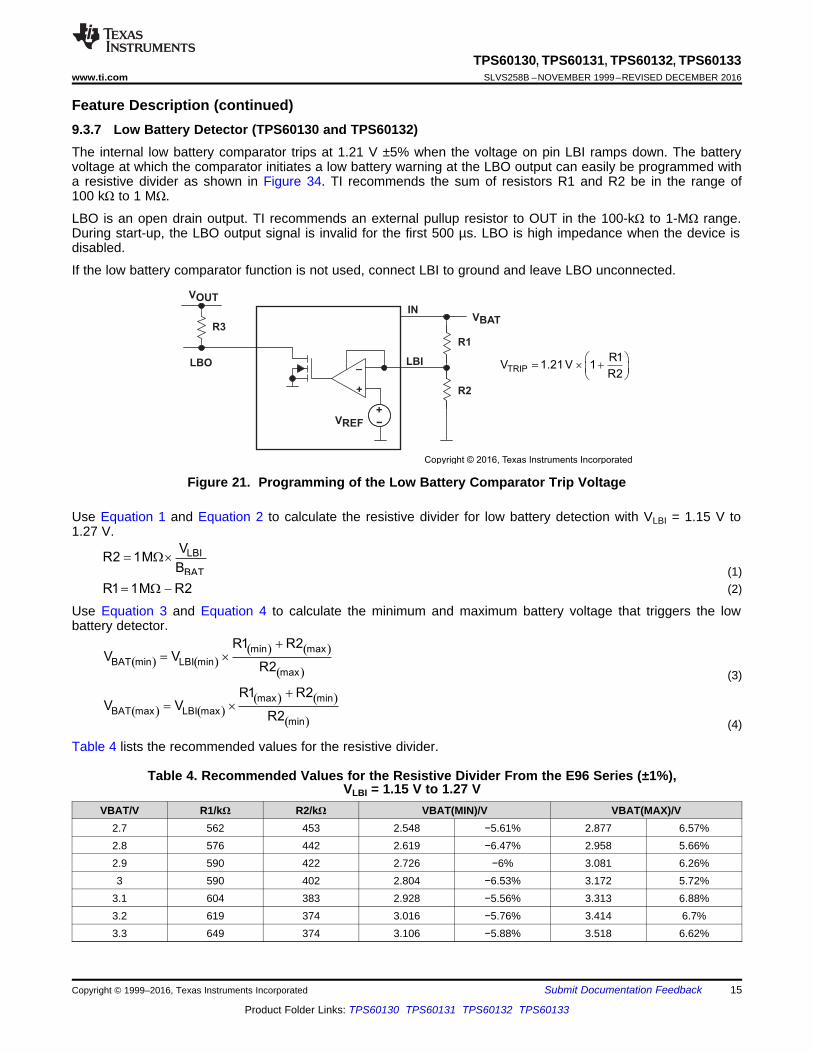
Feature Description (continued)9.3.7 Low Battery Detector (TPS60130 and TPS60132)The internal low battery comparator trips at 1.21 V ±5% when the voltage on pin LBI ramps down. The batteryvoltage at which the comparator initiates a low battery warning at the LBO output can easily be programmed witha resistive divider as shown in Figure 34. TI recommends the sum of resistors R1 and R2 be in the range of100 kΩ to 1 MΩ.
LBO is an open drain output. TI recommends an external pullup resistor to OUT in the 100-kΩ to 1-MΩ range.During start-up, the LBO output signal is invalid for the first 500 µs. LBO is high impedance when the device isdisabled.
If the low battery comparator function is not used, connect LBI to ground and leave LBO unconnected.
Figure 21. Programming of the Low Battery Comparator Trip Voltage
Use Equation 1 and Equation 2 to calculate the resistive divider for low battery detection with VLBI = 1.15 V to1.27 V.
(1)(2)
Use Equation 3 and Equation 4 to calculate the minimum and maximum battery voltage that triggers the lowbattery detector.
(3)
(4)
Table 4 lists the recommended values for the resistive divider.
Table 4. Recommended Values for the Resistive Divider From the E96 Series (±1%),VLBI = 1.15 V to 1.27 V
VBAT/V R1/kΩ R2/kΩ VBAT(MIN)/V VBAT(MAX)/V2.7 562 453 2.548 −5.61% 2.877 6.57%2.8 576 442 2.619 −6.47% 2.958 5.66%2.9 590 422 2.726 −6% 3.081 6.26%3 590 402 2.804 −6.53% 3.172 5.72%
3.1 604 383 2.928 −5.56% 3.313 6.88%3.2 619 374 3.016 −5.76% 3.414 6.7%3.3 649 374 3.106 −5.88% 3.518 6.62%

Copyright © 2016, Texas Instruments Incorporated
16
TPS60130, TPS60131, TPS60132, TPS60133SLVS258B –NOVEMBER 1999–REVISED DECEMBER 2016 www.ti.com
Product Folder Links: TPS60130 TPS60131 TPS60132 TPS60133
Submit Documentation Feedback Copyright © 1999–2016, Texas Instruments Incorporated
A 100-nF bypass capacitor must be connected in parallel to R2 if large line transients are expected. Thesevoltage drops can inadvertently trigger the low battery comparator and produce a wrong low battery warningsignal at the LBO pin.
9.3.8 Power Good Detector (TPS60131 and TPS60133)The PG pin is an open-drain output that is pulled low when the output is out of regulation. When the outputvoltage rises to about 90% of its nominal voltage, Power Good output is released. PG is high impedance whenthe device is disabled. An external pullup resistor must be connected between PG and OUT. The pullup resistormust be in the 100-kΩ to 1-MΩ range. If the Power Good function is not used, the PG-pin must remainunconnected.
Figure 22. Typical Operating Circuit Using Power Good Comparator

Copyright © 2016, Texas Instruments Incorporated
17
TPS60130, TPS60131, TPS60132, TPS60133www.ti.com SLVS258B –NOVEMBER 1999–REVISED DECEMBER 2016
Product Folder Links: TPS60130 TPS60131 TPS60132 TPS60133
Submit Documentation FeedbackCopyright © 1999–2016, Texas Instruments Incorporated
10 Application and Implementation
NOTEInformation in the following applications sections is not part of the TI componentspecification, and TI does not warrant its accuracy or completeness. TI’s customers areresponsible for determining suitability of components for their purposes. Customers shouldvalidate and test their design implementation to confirm system functionality.
10.1 Application InformationThe TPS6013x charge pumps provide a regulated 5-V output from a 2.7-V to 5.4-V input. They deliver amaximum load current of 300 mA or 150 mA (respectively).
10.2 Typical Applications
10.2.1 Paralleling of Two TPS6013x to Deliver 600-mA Total Output CurrentTwo TPS60130x devices can be connected in parallel to yield higher load currents. The circuit of Figure 23 candeliver up to 600 mA at an output voltage of 5 V.
Figure 23. Paralleling of Two TPS6013x Charge Pumps
10.2.1.1 Design RequirementsThe device operates over an input voltage range from 2.7 V to 5.4 V.
10.2.1.2 Detailed Design ProcedureThe devices can share the output capacitors, but each one requires its own transfer capacitors and inputcapacitor. If both a TPS60130 and a TPS60131 are used, it is possible to monitor the battery voltage with theTPS60130 using the low battery comparator function and to supervise the output voltage with the TPS60131using the Power Good comparator. Make the layout of the charge pumps as similar as possible, and position theoutput capacitor the same distance from both devices.
10.2.1.2.1 Capacitor Selection
The TPS6013x charge pump require only four external capacitors as shown in the basic application circuit. Theircapacitance values and types are closely linked to the output current and output noise and ripple requirements.For lowest noise and ripple, low ESR (<0.1 Ω) capacitors must be used for input and output capacitors.
The input capacitor improves system efficiency by reducing the input impedance. It also stabilizes the inputcurrent of the power source. The input capacitor must be chosen according to the power supply used and thedistance from power source to the converter IC. The input capacitor also has an impact on the output voltageripple. The lower the ESR of the input capacitor Ci, the lower is the output ripple. TI recommends Ci be about twoto four times as large as C(xF).
18
TPS60130, TPS60131, TPS60132, TPS60133SLVS258B –NOVEMBER 1999–REVISED DECEMBER 2016 www.ti.com
Product Folder Links: TPS60130 TPS60131 TPS60132 TPS60133
Submit Documentation Feedback Copyright © 1999–2016, Texas Instruments Incorporated
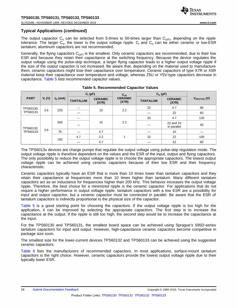
Typical Applications (continued)The output capacitor Co can be selected from 5-times to 50-times larger than C(xF), depending on the rippletolerance. The larger Co, the lower is the output voltage ripple. Ci and Co can be either ceramic or low-ESRtantalum; aluminum capacitors are not recommended.
Generally, the flying capacitors C(xF) is the smallest. Only ceramic capacitors are recommended, due to their lowESR and because they retain their capacitance at the switching frequency. Because the device regulates theoutput voltage using the pulse-skip technique, a larger flying capacitor leads to a higher output voltage ripple ifthe size of the output capacitor is not increased. Be aware that, depending on the material used to manufacturethem, ceramic capacitors might lose their capacitance over temperature. Ceramic capacitors of type X7R or X5Rmaterial keep their capacitance over temperature and voltage, whereas Z5U or Y5V-type capacitors decrease incapacitance. Table 5 lists recommended capacitor values.
Table 5. Recommended Capacitor Values
PART VI (V) IO (mA)Ci (µF) CxF
CERAMIC(X7R)
Co (µF)VPP(TYP) (V)
TANTALUM CERAMIC(X7R) TANTALUM CERAMIC
(X7R)
TPS60130,TPS60131 3.6 225
—10 2.2
22 4.7 90— — 22 60
TPS60132,TPS60133 3.6
300—
10 2.233 4.7 120
— — 22 and 10in parallel 45
75 — 4.71
— 10 —
1504.7 2.2 15 22 100— 4.7 — 22 90
The TPS6013x devices are charge pumps that regulate the output voltage using pulse-skip regulation mode. Theoutput voltage ripple is therefore dependent on the values and the ESR of the input, output and flying capacitors.The only possibility to reduce the output voltage ripple is to choose the appropriate capacitors. The lowest outputvoltage ripple can be achieved using ceramic capacitors because of their low ESR and their frequencycharacteristic.
Ceramic capacitors typically have an ESR that is more than 10 times lower than tantalum capacitors and theyretain their capacitance at frequencies more than 10 times higher than tantalum. Many different tantalumcapacitors act as an inductance for frequencies higher than 200 kHz. This behavior increases the output voltageripple. Therefore, the best choice for a minimized ripple is the ceramic capacitor. For applications that do notrequire a higher performance in output voltage ripple, tantalum capacitors with a low ESR are a possibility forinput and output capacitor, but a ceramic capacitor must be connected in parallel. Be aware that the ESR oftantalum capacitors is indirectly proportional to the physical size of the capacitor.
Table 5 is a good starting point for choosing the capacitors. If the output voltage ripple is too high for theapplication, it can be improved by selecting the appropriate capacitors. The first step is to increase thecapacitance at the output. If the ripple is still too high, the second step would be to increase the capacitance atthe input.
For the TPS60130 and TPS60131, the smallest board space can be achieved using Sprague’s 595D-seriestantalum capacitors for input and output. However, high-capacitance ceramic capacitors become competitive inpackage size soon.
The smallest size for the lower-current devices TPS60132 and TPS60133 can be achieved using the suggestedceramic capacitors.
Table 6 lists the manufacturers of recommended capacitors. In most applications, surface-mount tantalumcapacitors is the right choice. However, ceramic capacitors provide the lowest output voltage ripple due to theirtypically lower ESR.
19
TPS60130, TPS60131, TPS60132, TPS60133www.ti.com SLVS258B –NOVEMBER 1999–REVISED DECEMBER 2016
Product Folder Links: TPS60130 TPS60131 TPS60132 TPS60133
Submit Documentation FeedbackCopyright © 1999–2016, Texas Instruments Incorporated
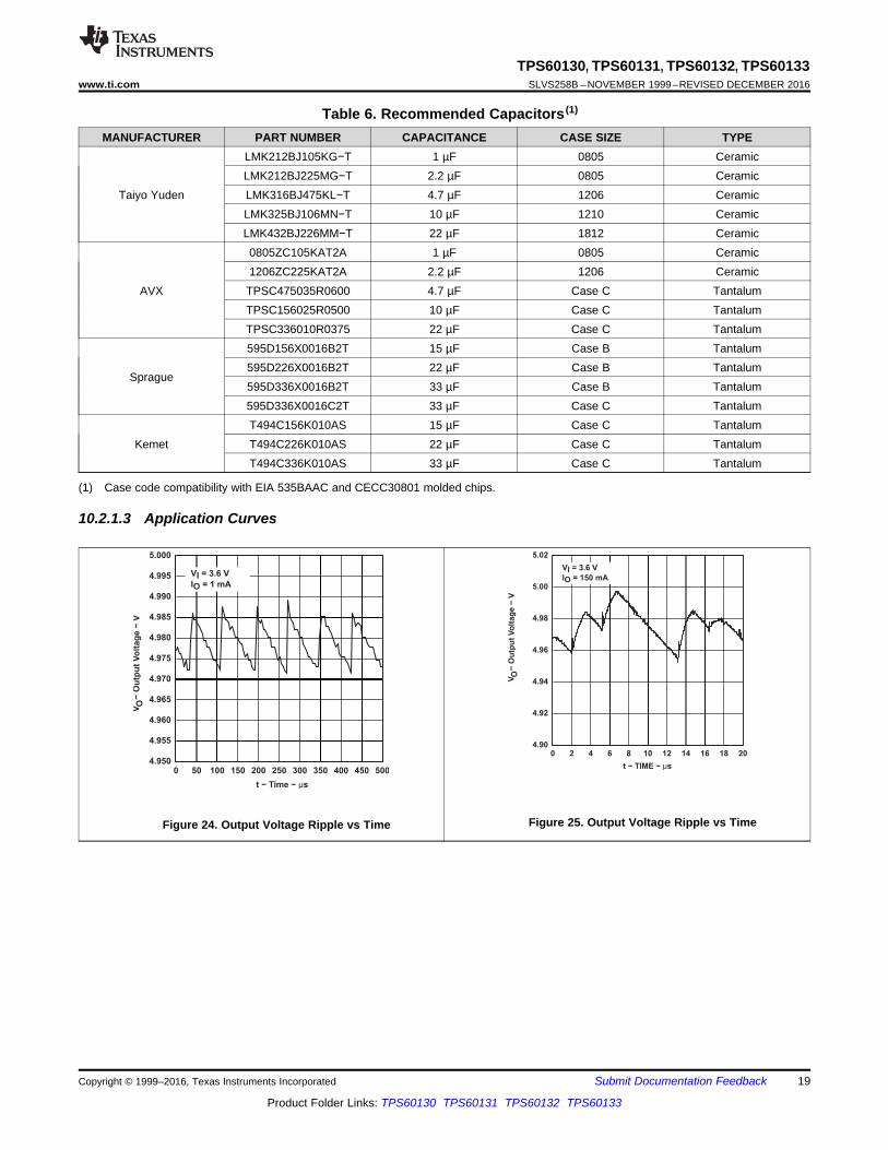
(1) Case code compatibility with EIA 535BAAC and CECC30801 molded chips.
Table 6. Recommended Capacitors (1)
MANUFACTURER PART NUMBER CAPACITANCE CASE SIZE TYPE
Taiyo Yuden
LMK212BJ105KG−T 1 µF 0805 CeramicLMK212BJ225MG−T 2.2 µF 0805 CeramicLMK316BJ475KL−T 4.7 µF 1206 CeramicLMK325BJ106MN−T 10 µF 1210 CeramicLMK432BJ226MM−T 22 µF 1812 Ceramic
AVX
0805ZC105KAT2A 1 µF 0805 Ceramic1206ZC225KAT2A 2.2 µF 1206 CeramicTPSC475035R0600 4.7 µF Case C TantalumTPSC156025R0500 10 µF Case C TantalumTPSC336010R0375 22 µF Case C Tantalum
Sprague
595D156X0016B2T 15 µF Case B Tantalum595D226X0016B2T 22 µF Case B Tantalum595D336X0016B2T 33 µF Case B Tantalum595D336X0016C2T 33 µF Case C Tantalum
KemetT494C156K010AS 15 µF Case C TantalumT494C226K010AS 22 µF Case C TantalumT494C336K010AS 33 µF Case C Tantalum
10.2.1.3 Application Curves
Figure 24. Output Voltage Ripple vs Time Figure 25. Output Voltage Ripple vs Time

20
TPS60130, TPS60131, TPS60132, TPS60133SLVS258B –NOVEMBER 1999–REVISED DECEMBER 2016 www.ti.com
Product Folder Links: TPS60130 TPS60131 TPS60132 TPS60133
Submit Documentation Feedback Copyright © 1999–2016, Texas Instruments Incorporated
Figure 26. Output Voltage Ripple vs Time Figure 27. Output Voltage Ripple Amplitudevs Input Voltage
Figure 28. Load Transient Response Figure 29. Line Transient Response
Figure 30. Output Voltage vs Time (Start-Up Timing)

Copyright © 2016, Texas Instruments Incorporated
Copyright © 2016, Texas Instruments Incorporated
21
TPS60130, TPS60131, TPS60132, TPS60133www.ti.com SLVS258B –NOVEMBER 1999–REVISED DECEMBER 2016
Product Folder Links: TPS60130 TPS60131 TPS60132 TPS60133
Submit Documentation FeedbackCopyright © 1999–2016, Texas Instruments Incorporated
10.2.2 TPS6013x Operated With Ultra-Low Quiescent CurrentBecause the output of the TPS6013x is isolated from the input when the devices are disabled, and because theinternal resistive divider is disconnected in shutdown, an ultra-low quiescent current mode can be implemented.In this mode, the output voltage is sustained because the converter is periodically enabled to refresh the outputcapacitor. The necessary external control signal that is applied to the ENABLE-pin is generated from amicrocontroller. For a necessary supply current for the system of 1 mA and a minimum supply voltage of 4.5 Vwith a 33-µF output capacitor, the refresh has to be done after 9 ms. Longer refresh periods can be achievedwith a larger output capacitor.
Figure 31. TPS60132 in Ultra-Low Quiescent Current Mode
10.2.2.1 Design RequirementsThe device operates over an input voltage range from 2.7 V to 5.4 V.
10.2.3 Regulated Discharge of the Output Capacitors After Disabling of the TPS6013xDuring shutdown of the charge pump TPS6013x the output is isolated from the input. Therefore, the dischargingof the output capacitor depends on the load and on the leakage current of the capacitor. In certain applications itis necessary to completely remove the supply voltage from the load in shutdown mode. That means the outputcapacitor of the charge pump has to be actively discharged when the charge pump is disabled. Figure 5 showsone solution to this problem.
Figure 32. Block Diagram of the Regulated Discharge of the Output Capacitor
10.2.3.1 Design RequirementsThe device operates over an input voltage range from 2.7 V to 5.4 V. TI's SN74AHC1G04 and BSS138 isrequired.

DISS O O
1P 1 V I
æ ö= - ´ç ÷hè ø
Vin
Vout
GND
EnableLBO
LBO
PGND
PGND
PGND
PGND
GND
GND
GND
GND
FB
OUT OUT
IN IN
C1-
C1+ C2+
C2-
LBIEN
22
TPS60130, TPS60131, TPS60132, TPS60133SLVS258B –NOVEMBER 1999–REVISED DECEMBER 2016 www.ti.com
Product Folder Links: TPS60130 TPS60131 TPS60132 TPS60133
Submit Documentation Feedback Copyright © 1999–2016, Texas Instruments Incorporated
11 Power Supply RecommendationsThe TPS6013x device has no special requirements for its input power supply. The output current of the inputpower supply must be rated according to the supply voltage, output voltage, and output current of the TPS6013x.
12 Layout
12.1 Layout GuidelinesCareful board layout is necessary due to the high transient currents and switching frequency of the converter. Allcapacitors must be soldered in close proximity to the IC. Connect ground and power ground pins through a short,low-impedance trace. A PCB layout proposal for a two-layer board is given in Figure 33. The bottom layer of theboard carries only ground potential for best performance. The layout also provides improved thermalperformance as the exposed lead frame is soldered to the PCB.
An evaluation module for the TPS60130 is available and can be ordered under product code TPS60130EVM-143. The EVM uses the layout shown in Figure 33 and components in Table 7.
The best performance of the converter is achieved with the additional bypass capacitors C5 and C6 at input andoutput. Capacitor C7 must be included if the large line transients are expected. The capacitors are not required.They can be omitted in most applications.
12.2 Layout Example
Figure 33. Recommended PCB Layout for TPS6013x
Table 7. Component IdentificationCOMPONENT DESCRIPTION
IC1 TPS6013xC1, C2 Flying capacitorsC3, C6 Input capacitorsC4, C5 Onput capacitors
C7 Stabilization capacitor for LBIR1, R2 Resistive divider for LBI
R3 Pullup resistor for LBO
12.3 Power DissipationThe power dissipated in the TPS6013x depends on output current and the mode of operation (1.5× or doublervoltage conversion mode). It is described by Equation 5.
(5)

23
TPS60130, TPS60131, TPS60132, TPS60133www.ti.com SLVS258B –NOVEMBER 1999–REVISED DECEMBER 2016
Product Folder Links: TPS60130 TPS60131 TPS60132 TPS60133
Submit Documentation FeedbackCopyright © 1999–2016, Texas Instruments Incorporated
Power Dissipation (continued)PDISS must be less than that allowed by the package rating. See Absolute Maximum Ratings for 20-pin PWPpackage power-dissipation limits and deratings.
Figure 34. Dissipation Derating Curvesvs Free-Air Temperature
Figure 35. Maximum Continuous Dissipationvs Case Temperature

24
TPS60130, TPS60131, TPS60132, TPS60133SLVS258B –NOVEMBER 1999–REVISED DECEMBER 2016 www.ti.com
Product Folder Links: TPS60130 TPS60131 TPS60132 TPS60133
Submit Documentation Feedback Copyright © 1999–2016, Texas Instruments Incorporated
13 Device and Documentation Support
13.1 Documentation Support
13.1.1 Related DocumentationFor related documentation see the following:• PowerPAD™ Application Report (SLMA002)• TPS6010x/TPS6011x Charge Pump Application Report (SLVA070)• Powering the TMS320C5420 Using the TPS60100, TPS76918, and the TPS3305-18 (SLVA082)• Evaluation Modules (EVMs) for TPS6012x and TPS6013x (SLVU022)
13.2 Related LinksThe table below lists quick access links. Categories include technical documents, support and communityresources, tools and software, and quick access to sample or buy.
Table 8. Related Links
PARTS PRODUCT FOLDER SAMPLE & BUY TECHNICALDOCUMENTS
TOOLS &SOFTWARE
SUPPORT &COMMUNITY
TPS60130 Click here Click here Click here Click here Click hereTPS60131 Click here Click here Click here Click here Click hereTPS60132 Click here Click here Click here Click here Click hereTPS60133 Click here Click here Click here Click here Click here
13.3 Receiving Notification of Documentation UpdatesTo receive notification of documentation updates, navigate to the device product folder on ti.com. In the upperright corner, click on Alert me to register and receive a weekly digest of any product information that haschanged. For change details, review the revision history included in any revised document.
13.4 Community ResourcesThe following links connect to TI community resources. Linked contents are provided "AS IS" by the respectivecontributors. They do not constitute TI specifications and do not necessarily reflect TI's views; see TI's Terms ofUse.
TI E2E™ Online Community TI's Engineer-to-Engineer (E2E) Community. Created to foster collaborationamong engineers. At e2e.ti.com, you can ask questions, share knowledge, explore ideas and helpsolve problems with fellow engineers.
Design Support TI's Design Support Quickly find helpful E2E forums along with design support tools andcontact information for technical support.
13.5 TrademarksPowerPAD, E2E are trademarks of Texas Instruments.All other trademarks are the property of their respective owners.
13.6 Electrostatic Discharge CautionThese devices have limited built-in ESD protection. The leads should be shorted together or the device placed in conductive foamduring storage or handling to prevent electrostatic damage to the MOS gates.
13.7 GlossarySLYZ022 — TI Glossary.
This glossary lists and explains terms, acronyms, and definitions.

25
TPS60130, TPS60131, TPS60132, TPS60133www.ti.com SLVS258B –NOVEMBER 1999–REVISED DECEMBER 2016
Product Folder Links: TPS60130 TPS60131 TPS60132 TPS60133
Submit Documentation FeedbackCopyright © 1999–2016, Texas Instruments Incorporated
14 Mechanical, Packaging, and Orderable InformationThe following pages include mechanical, packaging, and orderable information. This information is the mostcurrent data available for the designated devices. This data is subject to change without notice and revision ofthis document. For browser-based versions of this data sheet, refer to the left-hand navigation.

PACKAGE OPTION ADDENDUM
www.ti.com 12-Aug-2016
Addendum-Page 1
PACKAGING INFORMATION
Orderable Device Status(1)
Package Type PackageDrawing
Pins PackageQty
Eco Plan(2)
Lead/Ball Finish(6)
MSL Peak Temp(3)
Op Temp (°C) Device Marking(4/5)
Samples
TPS60130PWP ACTIVE HTSSOP PWP 20 70 Green (RoHS& no Sb/Br)
CU NIPDAU Level-2-260C-1 YEAR -40 to 85 TPS60130
TPS60130PWPG4 ACTIVE HTSSOP PWP 20 70 Green (RoHS& no Sb/Br)
CU NIPDAU Level-2-260C-1 YEAR -40 to 85 TPS60130
TPS60130PWPR ACTIVE HTSSOP PWP 20 2000 Green (RoHS& no Sb/Br)
CU NIPDAU Level-2-260C-1 YEAR -40 to 85 TPS60130
TPS60131PWP ACTIVE HTSSOP PWP 20 70 Green (RoHS& no Sb/Br)
CU NIPDAU Level-2-260C-1 YEAR -40 to 85 TPS60131
TPS60131PWPG4 ACTIVE HTSSOP PWP 20 70 Green (RoHS& no Sb/Br)
CU NIPDAU Level-2-260C-1 YEAR -40 to 85 TPS60131
TPS60131PWPR ACTIVE HTSSOP PWP 20 2000 Green (RoHS& no Sb/Br)
CU NIPDAU Level-2-260C-1 YEAR -40 to 85 TPS60131
TPS60131PWPRG4 ACTIVE HTSSOP PWP 20 2000 Green (RoHS& no Sb/Br)
CU NIPDAU Level-2-260C-1 YEAR -40 to 85 TPS60131
TPS60132PWP ACTIVE HTSSOP PWP 20 70 Green (RoHS& no Sb/Br)
CU NIPDAU Level-2-260C-1 YEAR -40 to 85 TPS60132
TPS60132PWPG4 ACTIVE HTSSOP PWP 20 70 Green (RoHS& no Sb/Br)
CU NIPDAU Level-2-260C-1 YEAR -40 to 85 TPS60132
TPS60133PWP ACTIVE HTSSOP PWP 20 70 Green (RoHS& no Sb/Br)
CU NIPDAU Level-2-260C-1 YEAR -40 to 85 TPS60133
TPS60133PWPG4 ACTIVE HTSSOP PWP 20 70 Green (RoHS& no Sb/Br)
CU NIPDAU Level-2-260C-1 YEAR -40 to 85 TPS60133
TPS60133PWPR ACTIVE HTSSOP PWP 20 2000 Green (RoHS& no Sb/Br)
CU NIPDAU Level-2-260C-1 YEAR -40 to 85 TPS60133
(1) The marketing status values are defined as follows:ACTIVE: Product device recommended for new designs.LIFEBUY: TI has announced that the device will be discontinued, and a lifetime-buy period is in effect.NRND: Not recommended for new designs. Device is in production to support existing customers, but TI does not recommend using this part in a new design.PREVIEW: Device has been announced but is not in production. Samples may or may not be available.OBSOLETE: TI has discontinued the production of the device.
(2) Eco Plan - The planned eco-friendly classification: Pb-Free (RoHS), Pb-Free (RoHS Exempt), or Green (RoHS & no Sb/Br) - please check http://www.ti.com/productcontent for the latest availabilityinformation and additional product content details.TBD: The Pb-Free/Green conversion plan has not been defined.

PACKAGE OPTION ADDENDUM
www.ti.com 12-Aug-2016
Addendum-Page 2
Pb-Free (RoHS): TI's terms "Lead-Free" or "Pb-Free" mean semiconductor products that are compatible with the current RoHS requirements for all 6 substances, including the requirement thatlead not exceed 0.1% by weight in homogeneous materials. Where designed to be soldered at high temperatures, TI Pb-Free products are suitable for use in specified lead-free processes.Pb-Free (RoHS Exempt): This component has a RoHS exemption for either 1) lead-based flip-chip solder bumps used between the die and package, or 2) lead-based die adhesive used betweenthe die and leadframe. The component is otherwise considered Pb-Free (RoHS compatible) as defined above.Green (RoHS & no Sb/Br): TI defines "Green" to mean Pb-Free (RoHS compatible), and free of Bromine (Br) and Antimony (Sb) based flame retardants (Br or Sb do not exceed 0.1% by weightin homogeneous material)
(3) MSL, Peak Temp. - The Moisture Sensitivity Level rating according to the JEDEC industry standard classifications, and peak solder temperature.
(4) There may be additional marking, which relates to the logo, the lot trace code information, or the environmental category on the device.
(5) Multiple Device Markings will be inside parentheses. Only one Device Marking contained in parentheses and separated by a "~" will appear on a device. If a line is indented then it is a continuationof the previous line and the two combined represent the entire Device Marking for that device.
(6) Lead/Ball Finish - Orderable Devices may have multiple material finish options. Finish options are separated by a vertical ruled line. Lead/Ball Finish values may wrap to two lines if the finishvalue exceeds the maximum column width.
Important Information and Disclaimer:The information provided on this page represents TI's knowledge and belief as of the date that it is provided. TI bases its knowledge and belief on informationprovided by third parties, and makes no representation or warranty as to the accuracy of such information. Efforts are underway to better integrate information from third parties. TI has taken andcontinues to take reasonable steps to provide representative and accurate information but may not have conducted destructive testing or chemical analysis on incoming materials and chemicals.TI and TI suppliers consider certain information to be proprietary, and thus CAS numbers and other limited information may not be available for release.
In no event shall TI's liability arising out of such information exceed the total purchase price of the TI part(s) at issue in this document sold by TI to Customer on an annual basis.

TAPE AND REEL INFORMATION
*All dimensions are nominal
Device PackageType
PackageDrawing
Pins SPQ ReelDiameter
(mm)
ReelWidth
W1 (mm)
A0(mm)
B0(mm)
K0(mm)
P1(mm)
W(mm)
Pin1Quadrant
TPS60130PWPR HTSSOP PWP 20 2000 330.0 16.4 6.95 7.1 1.6 8.0 16.0 Q1
TPS60131PWPR HTSSOP PWP 20 2000 330.0 16.4 6.95 7.1 1.6 8.0 16.0 Q1
TPS60133PWPR HTSSOP PWP 20 2000 330.0 16.4 6.95 7.1 1.6 8.0 16.0 Q1
PACKAGE MATERIALS INFORMATION
www.ti.com 29-Feb-2016
Pack Materials-Page 1

*All dimensions are nominal
Device Package Type Package Drawing Pins SPQ Length (mm) Width (mm) Height (mm)
TPS60130PWPR HTSSOP PWP 20 2000 367.0 367.0 38.0
TPS60131PWPR HTSSOP PWP 20 2000 367.0 367.0 38.0
TPS60133PWPR HTSSOP PWP 20 2000 367.0 367.0 38.0
PACKAGE MATERIALS INFORMATION
www.ti.com 29-Feb-2016
Pack Materials-Page 2

IMPORTANT NOTICE
Texas Instruments Incorporated and its subsidiaries (TI) reserve the right to make corrections, enhancements, improvements and otherchanges to its semiconductor products and services per JESD46, latest issue, and to discontinue any product or service per JESD48, latestissue. Buyers should obtain the latest relevant information before placing orders and should verify that such information is current andcomplete. All semiconductor products (also referred to herein as “components”) are sold subject to TI’s terms and conditions of salesupplied at the time of order acknowledgment.TI warrants performance of its components to the specifications applicable at the time of sale, in accordance with the warranty in TI’s termsand conditions of sale of semiconductor products. Testing and other quality control techniques are used to the extent TI deems necessaryto support this warranty. Except where mandated by applicable law, testing of all parameters of each component is not necessarilyperformed.TI assumes no liability for applications assistance or the design of Buyers’ products. Buyers are responsible for their products andapplications using TI components. To minimize the risks associated with Buyers’ products and applications, Buyers should provideadequate design and operating safeguards.TI does not warrant or represent that any license, either express or implied, is granted under any patent right, copyright, mask work right, orother intellectual property right relating to any combination, machine, or process in which TI components or services are used. Informationpublished by TI regarding third-party products or services does not constitute a license to use such products or services or a warranty orendorsement thereof. Use of such information may require a license from a third party under the patents or other intellectual property of thethird party, or a license from TI under the patents or other intellectual property of TI.Reproduction of significant portions of TI information in TI data books or data sheets is permissible only if reproduction is without alterationand is accompanied by all associated warranties, conditions, limitations, and notices. TI is not responsible or liable for such altereddocumentation. Information of third parties may be subject to additional restrictions.Resale of TI components or services with statements different from or beyond the parameters stated by TI for that component or servicevoids all express and any implied warranties for the associated TI component or service and is an unfair and deceptive business practice.TI is not responsible or liable for any such statements.Buyer acknowledges and agrees that it is solely responsible for compliance with all legal, regulatory and safety-related requirementsconcerning its products, and any use of TI components in its applications, notwithstanding any applications-related information or supportthat may be provided by TI. Buyer represents and agrees that it has all the necessary expertise to create and implement safeguards whichanticipate dangerous consequences of failures, monitor failures and their consequences, lessen the likelihood of failures that might causeharm and take appropriate remedial actions. Buyer will fully indemnify TI and its representatives against any damages arising out of the useof any TI components in safety-critical applications.In some cases, TI components may be promoted specifically to facilitate safety-related applications. With such components, TI’s goal is tohelp enable customers to design and create their own end-product solutions that meet applicable functional safety standards andrequirements. Nonetheless, such components are subject to these terms.No TI components are authorized for use in FDA Class III (or similar life-critical medical equipment) unless authorized officers of the partieshave executed a special agreement specifically governing such use.Only those TI components which TI has specifically designated as military grade or “enhanced plastic” are designed and intended for use inmilitary/aerospace applications or environments. Buyer acknowledges and agrees that any military or aerospace use of TI componentswhich have not been so designated is solely at the Buyer's risk, and that Buyer is solely responsible for compliance with all legal andregulatory requirements in connection with such use.TI has specifically designated certain components as meeting ISO/TS16949 requirements, mainly for automotive use. In any case of use ofnon-designated products, TI will not be responsible for any failure to meet ISO/TS16949.
Products ApplicationsAudio www.ti.com/audio Automotive and Transportation www.ti.com/automotiveAmplifiers amplifier.ti.com Communications and Telecom www.ti.com/communicationsData Converters dataconverter.ti.com Computers and Peripherals www.ti.com/computersDLP® Products www.dlp.com Consumer Electronics www.ti.com/consumer-appsDSP dsp.ti.com Energy and Lighting www.ti.com/energyClocks and Timers www.ti.com/clocks Industrial www.ti.com/industrialInterface interface.ti.com Medical www.ti.com/medicalLogic logic.ti.com Security www.ti.com/securityPower Mgmt power.ti.com Space, Avionics and Defense www.ti.com/space-avionics-defenseMicrocontrollers microcontroller.ti.com Video and Imaging www.ti.com/videoRFID www.ti-rfid.comOMAP Applications Processors www.ti.com/omap TI E2E Community e2e.ti.comWireless Connectivity www.ti.com/wirelessconnectivity
Mailing Address: Texas Instruments, Post Office Box 655303, Dallas, Texas 75265Copyright © 2016, Texas Instruments Incorporated


![COVID-19 Useful links€¦ · Useful links: COVID-19 G FOLDER [UK] Advice for remuneration committees on COVID-19 COVID-19 response: example reward and performance checklist COVID](https://img.pdfslide.net/doc/110x75/5f94bdba77ac112aa063f61f/covid-19-useful-links-useful-links-covid-19-g-folder-uk-advice-for-remuneration.jpg)