Embed Size (px)
Citation preview
VIN
GND VOUT
C1
C2
L1Total area
is less than
12mm²
CIN2.2 µF
VIN2.05 V to 6 V
COUT4.7 µF
VOUT1.8 V
L1 µH or 2.2 µHTPS62231-Q1
VIN
EN
MODE
SW
FB
GND
Product
Folder
Sample &Buy
Technical
Documents
Tools &
Software
Support &Community
ReferenceDesign
An IMPORTANT NOTICE at the end of this data sheet addresses availability, warranty, changes, use in safety-critical applications,intellectual property matters and other important disclaimers. PRODUCTION DATA.
TPS62231-Q1, TPS622314-Q1SLVSB63A –DECEMBER 2011–REVISED MARCH 2016
TPS62231x-Q1 3-MHz Ultra-Small Step-Down Converter in 1 × 1.5 SON Package
1
1 Features1• Qualified for Automotive Applications• Up to 3.8-MHz Switch Frequency• Up to 94% Efficiency• Output Peak Current up to 500 mA• Excellent AC and Transient Load Regulation• High PSRR (up to 90 dB)• Small External Output-Filter Components 1 μH
and 4.7 μF• VIN range from 2.05 V to 6 V• Optimized Power Save Mode For Low Output-
Ripple Voltage• Forced PWM Mode Operation• Typical 22-μA Quiescent Current• 100% Duty Cycle for Lowest Dropout• Small 1 × 1.5 × 0.6-mm3 SON Package• 12-mm2 Minimum Solution Size• Supports 0.6-mm Maximum Solution Height• Soft Start With 100-μs (Typical) Start-Up Time
2 Applications• Advanced Driver-Assistance System (ADAS)
– Front Camera, Rear View Camera– Surround View– Blind-Spot Monitoring
• Automotive Telematics, eCall, and Tolling• Space-Optimized Automotive and Industrial Power
Systems
3 DescriptionThe TPS6223x-Q1 device family is a high-frequency,synchronous step-down DC-DC converter ideal forspace-optimized automotive and industrialapplications. The device supports up to 500-mAoutput current and allows the use of tiny and low-costchip inductors and capacitors.
With a wide input-voltage range of 2.05 V to 6 V, thedevice can be powered by a preregulated voltage railor Li-Ion batteries with extended voltage range. Twodifferent fixed-output voltage versions are available at1.5 V and 1.8 V.
The TPS6223x-Q1 series features switch frequencyup to 3.8 MHz. At medium to heavy loads, theconverter operates in PWM mode and automaticallyenters Power Save Mode operation at light loadcurrents to maintain high efficiency over the entireload current range.
Because of its excellent PSRR and AC loadregulation performance, the device is also suitable toreplace linear regulators to obtain better powerconversion efficiency.
The Power Save Mode in TPS6223x-Q1 reduces thequiescent current consumption down to 22 μA duringlight load operation. It is optimized to achieve verylow output voltage ripple even with small externalcomponent and features excellent AC load regulation.
For noise-sensitive applications, the device can beforced to PWM Mode operation over the entire loadrange by pulling the MODE pin high. In the shutdownmode, the current consumption is reduced to lessthan 1 μA. The TPS6223x-Q1 is available in a 1-mm× 1.5-mm2 6-pin SON package.
Device Information(1)
PART NUMBER OUTPUTVOLTAGE FREQUENCY
TPS62231-Q1 1.8 V 3 MHzTPS622314-Q1 1.5 V 3 MHz
(1) For all available packages, see the orderable addendum atthe end of the data sheet.
Typical Application Schematic Small PCB Layout Size
2
TPS62231-Q1, TPS622314-Q1SLVSB63A –DECEMBER 2011–REVISED MARCH 2016 www.ti.com
Product Folder Links: TPS62231-Q1 TPS622314-Q1
Submit Documentation Feedback Copyright © 2011–2016, Texas Instruments Incorporated
Table of Contents1 Features .................................................................. 12 Applications ........................................................... 13 Description ............................................................. 14 Revision History..................................................... 25 pPin Configuration and Functions....................... 36 Specifications......................................................... 3
6.1 Absolute Maximum Ratings ...................................... 36.2 ESD Ratings.............................................................. 46.3 Recommended Operating Conditions....................... 46.4 Thermal Information .................................................. 46.5 Electrical Characteristics........................................... 56.6 Typical Characteristics .............................................. 6
7 Detailed Description .............................................. 77.1 Overview ................................................................... 77.2 Functional Block Diagram ......................................... 77.3 Feature Description................................................... 87.4 Device Functional Modes.......................................... 8
8 Application and Implementation ........................ 108.1 Application Information............................................ 108.2 Typical Application .................................................. 10
9 Power Supply Recommendations ...................... 1610 Layout................................................................... 16
10.1 Layout Guidelines ................................................. 1610.2 Layout Example .................................................... 16
11 Device and Documentation Support ................. 1711.1 Device Support...................................................... 1711.2 Documentation Support ........................................ 1711.3 Related Links ........................................................ 1711.4 Community Resource............................................ 1711.5 Trademarks ........................................................... 1711.6 Electrostatic Discharge Caution............................ 1711.7 Glossary ................................................................ 17
12 Mechanical, Packaging, and OrderableInformation ........................................................... 18
4 Revision HistoryNOTE: Page numbers for previous revisions may differ from page numbers in the current version.
Changes from Original (December 2011) to Revision A Page
• Added Pin Configuration and Functions section, ESD Ratings table, Thermal Information table, Feature Descriptionsection, Device Functional Modes, Application and Implementation section, Power Supply Recommendationssection, Layout section, Device and Documentation Support section, and Mechanical, Packaging, and OrderableInformation section ................................................................................................................................................................. 1
• Changed the Applications list ................................................................................................................................................ 1• Deleted the Ordering Information table ................................................................................................................................. 1• Deleted references to devices and voltage options that are not available as automotive grade ........................................... 1• Added minimum and maximum recommended values for output inductance and output capacitance in the
Recommended Operating Conditions table for clarity............................................................................................................ 4• Deleted the Dissipation Ratings table and added a more detailed Thermal Information table .............................................. 4• Deleted the Parameter Measurement Information section..................................................................................................... 7
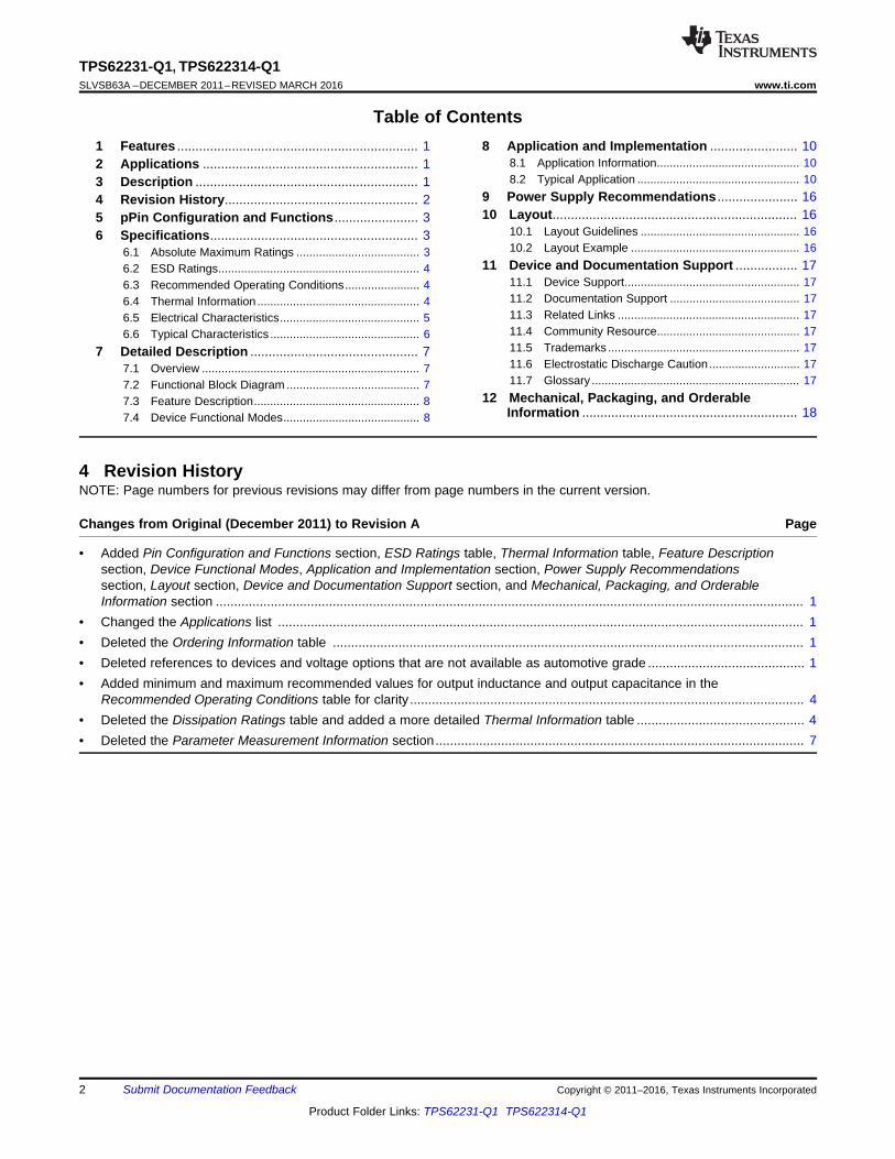
1MODE 6 FB
2SW 5 EN
3VIN 4 GND
3
TPS62231-Q1, TPS622314-Q1www.ti.com SLVSB63A –DECEMBER 2011–REVISED MARCH 2016
Product Folder Links: TPS62231-Q1 TPS622314-Q1
Submit Documentation FeedbackCopyright © 2011–2016, Texas Instruments Incorporated
5 pPin Configuration and Functions
DRY Package6-Pin SONTop View
Pin FunctionsPIN
TYPE DESCRIPTIONNO. NAME
1 MODE INWhen the MODE pin is high, the device is forced to operate in PWM mode. When the MODE pin is low, thepower save mode is enabled with automatic transition from PFM (pulse frequency mode) to PWM (pulsewidth modulation) mode. This pin must be terminated.
2 SW OUT This pin is the switch pin and is connected to the internal MOSFET switches. Connect the inductor to thispin.
3 VIN PWR VIN power supply pin.4 GND PWR GND supply pin.
5 EN IN This is the enable pin of the device. Pulling this pin to low forces the device into shutdown mode. Pullingthis pin to high enables the device. This pin must be terminated.
6 FB IN Feedback pin for the internal regulation loop. Connect this pin directly to the output capacitor.
(1) Stresses beyond those listed under Absolute Maximum Ratings may cause permanent damage to the device. These are stress ratingsonly, which do not imply functional operation of the device at these or any other conditions beyond those indicated under RecommendedOperating Conditions. Exposure to absolute-maximum-rated conditions for extended periods may affect device reliability.
(2) All voltage values are with respect to network ground terminal.
6 Specifications
6.1 Absolute Maximum Ratingsover operating free-air temperature range (unless otherwise noted) (1)
MIN MAX UNIT
VI
Voltage at VIN and SW pin (2) –0.3 7 VVoltage at EN, MODE pin (2) –0.3 (VIN + 0.3) ≤7 VVoltage at FB pin (2) –0.3 3.6 VPeak output current internally limited APower dissipation Internally limited
TJ Maximum operating junction temperature –40 125 °CTstg Storage temperature –65 150 °C
4
TPS62231-Q1, TPS622314-Q1SLVSB63A –DECEMBER 2011–REVISED MARCH 2016 www.ti.com
Product Folder Links: TPS62231-Q1 TPS622314-Q1
Submit Documentation Feedback Copyright © 2011–2016, Texas Instruments Incorporated
(1) AEC Q100-002 indicates that HBM stressing shall be in accordance with the ANSI/ESDA/JEDEC JS-001 specification.
6.2 ESD RatingsVALUE UNIT
V(ESD) Electrostatic dischargeHuman-body model (HBM), per AEC Q100-002 (1) ±2000
VCharged-device model (CDM), per AEC Q100-011 ±1000Machine Model (MM) 200
(1) In applications where high power dissipation, poor package thermal resistance, or both are present, the maximum ambient temperaturemay have to be derated. Maximum ambient temperature (TA(max)) is dependent on the maximum operating junction temperature(TJ(max)), the maximum power dissipation of the device in the application (PD(max)), and the junction-to-ambient thermal resistance of thepart/package in the application (RθJA), as given by the following equation: TA(max) = TJ(max) – (RθJA × PD(max)).
(2) The minimum required supply voltage for start-up is 2.05 V. The device is functional down to the falling UVLO (undervoltage lockout)threshold.
(3) For a voltage difference between minimum VIN and VOUT of ≥ 1 V(4) Typical value applies for TA = 25°C, maximum value applies for TA = 105°C with TJ ≤ 125°C, PCB layout needs to support proper
thermal performance.
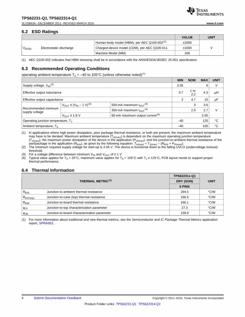
6.3 Recommended Operating Conditionsoperating ambient temperature TA = –40 to 105°C (unless otherwise noted) (1)
MIN NOM MAX UNITSupply voltage, VIN
(2) 2.05 6 V
Effective output inductance 0.7 1 or2.2 4.3 μH
Effective output capacitance 2 4.7 15 μF
Recommended minimumsupply voltage
VOUT ≤ (VIN – 1 V) (3) 500-mA maximum IOUT(4) 3 3.6
V350-mA maximum IOUT(4) 2.5 2.7
VOUT ≤ 1.8 V 60-mA maximum output current (4) 2.05Operating junction temperature, TJ –40 125 °CAmbient temperature, TA –40 105 °C
(1) For more information about traditional and new thermal metrics, see the Semiconductor and IC Package Thermal Metrics applicationreport, SPRA953.
6.4 Thermal Information
THERMAL METRIC (1)TPS62231x-Q1
UNITDRY (SON)6 PINS
RθJA Junction-to-ambient thermal resistance 294.5 °C/WRθJC(top) Junction-to-case (top) thermal resistance 166.5 °C/WRθJB Junction-to-board thermal resistance 166.1 °C/WψJT Junction-to-top characterization parameter 27.3 °C/WψJB Junction-to-board characterization parameter 159.9 °C/W
5
TPS62231-Q1, TPS622314-Q1www.ti.com SLVSB63A –DECEMBER 2011–REVISED MARCH 2016
Product Folder Links: TPS62231-Q1 TPS622314-Q1
Submit Documentation FeedbackCopyright © 2011–2016, Texas Instruments Incorporated
(1) In applications where high power dissipation and/or poor package thermal resistance is present, the maximum ambient temperature mayhave to be derated. Maximum ambient temperature (TA(max)) is dependent on the maximum operating junction temperature (TJ(max)), themaximum power dissipation of the device in the application (PD(max)), and the junction-to-ambient thermal resistance of the part/packagein the application (RθJA), as given by the following equation: TA(max) = TJ(max) – (RθJA × PD(max)).
(2) The minimum required supply voltage for start-up is 2.05 V. The device is functional down to the falling UVLO (undervoltage lockout)threshold
(3) Shutdown current into VIN pin, includes internal leakage(4) VIN = VO + 1 V(5) The internal resistor divider network is disconnected from FB pin.
6.5 Electrical CharacteristicsVIN = 3.6 V, VOUT = 1.8 V, EN = VIN, MODE = GND, TA = –40°C to 105°C (1), CIN = 2.2 μF, L = 2.2 μH, COUT = 4.7 μF, typicalvalues are at TA = 25°C (unless otherwise noted).
PARAMETER TEST CONDITIONS MIN TYP MAX UNITSUPPLYVIN Input voltage range (2) 2.05 6 V
IQ Operating quiescent current
IOUT = 0 mA. PFM mode enabled (MODE = 0)device not switching 22 40 μA
IOUT = 0 mA. PFM mode enabled (MODE = 0)device switching, VIN = 3.6 V, VOUT = 1.2 V 25 μA
IOUT = 0 mA. Switching with no load(MODE/DATA = VIN), PWM operation,VOUT = 1.8 V, L = 2.2 μH
3 mA
ISD Shutdown current EN = GND (3) 0.1 1 μA
UVLO Undervoltage-lockout thresholdFalling 1.8 1.9 VRising 1.9 2.05 V
ENABLE, MODE THRESHOLDVIH TH Threshold for detecting high EN, MODE 2.05 V ≤ VIN ≤ 6 V , rising edge 0.8 1 VVIL TH HYS Threshold for detecting low EN, MODE 2.05 V ≤ VIN ≤ 6 V , falling edge 0.4 0.6 VIIN Input bias Current, EN, MODE EN, MODE = GND or VIN = 3.6 V 0.01 0.5 μAPOWER SWITCH
RDS(ON)High-side MOSFET on-resistance VIN = 3.6 V, TJmax = 105°C; RDS(ON) max value 600 850
mΩLow-side MOSFET on-resistance VIN = 3.6 V, TJmax = 105°C; RDS(ON) max value 350 480
ILIMF
Forward current-limit MOSFET highside VIN = 3.6 V, open loop 690 850 1050 mA
Forward current-limit MOSFET low side VIN = 3.6 V, open loop 550 840 1220 mATSD Thermal shutdown Increasing junction temperature 150 °C
Thermal shutdown hysteresis Decreasing junction temperature 20 °CCONTROLLER
tONmin Minimum on time VIN = 3.6 V, VOUT = 1.8 V, Mode = high, IOUT = 0mA 135 ns
tOFFmin Minimum off time 40 nsOUTPUTVREF Internal reference voltage 0.70 V
VOUT
Output voltage accuracy (4)
VIN = 3.6 V, Mode = GND, device operating in PFMMode, IOUT = 0 mA 0%
VIN = 3.6 V, MODE = VIN,IOUT = 0 mA
TA = 25°C –2% 2%TA = –40°C to105°C –2.5% 2.5%
DC output voltage load regulation PWM operation, Mode = VIN = 3.6 V, VOUT = 1.8 V 0.001 %/mADC output voltage line regulation IOUT = 0 mA, Mode = VIN, 2.05 V ≤ VIN ≤ 6 V 0 %/V
tStart Start-up time Time from active EN to VOUT = 1.8 V, VIN = 3.6 V,10-Ω load 100 μs
ILK_SW Leakage current into SW pin VIN = VOUT = VSW = 3.6 V, EN = GND (5) 0.1 0.5 μA
PMOS
2 2.5 3 3.5 4 4.5 5 5.5 6
V - Input Voltage - VIN
0
0.2
0.4
0.6
0.8
1
1.2
1.4
1.6
1.8
2
r-
Sta
tic D
rain
-So
urc
e O
n-S
tate
Resis
tan
ce -
DS
(ON
)W
T = 85°CA
T = 60°CA
T = 25°CA
T = -40°CA
0
0.1
0.2
0.3
0.4
0.5
0.6
0.7
2 2.5 3 3.5 4 4.5 5 5.5 6
V - Input Voltage - VIN
r-
Sta
tic
Dra
in-S
ou
rce
On
-Sta
te R
es
ista
nc
e -
DS
(ON
)W
T = 85°CA
T = 60°CA
T = 25°CA
T = -40°CA
NMOS
10
15
20
25
30
35
I-
Qu
iescen
t C
urr
en
t -
AQ
m
2 2.5 3 3.5 4 4.5 5 5.5 6
V - Input Voltage - VIN
T = 85°CAT = 60°CA T = 25°CA
T = -40°CA
0
0.02
0.04
0.06
0.08
0.1
0.12
0.14
0.16
0.18
0.2
2 2.5 3 3.5 4 4.5 5 5.5 6
T = 85°CA
T = 60°CA T = 25°CAT = -40°CA
I-
Sh
utd
ow
n C
urr
en
t -
AS
Dm
V - Input Voltage - VIN
6
TPS62231-Q1, TPS622314-Q1SLVSB63A –DECEMBER 2011–REVISED MARCH 2016 www.ti.com
Product Folder Links: TPS62231-Q1 TPS622314-Q1
Submit Documentation Feedback Copyright © 2011–2016, Texas Instruments Incorporated
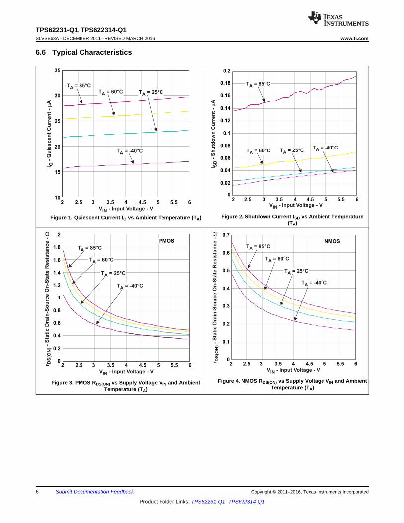
6.6 Typical Characteristics
Figure 1. Quiescent Current IQ vs Ambient Temperature (TA) Figure 2. Shutdown Current ISD vs Ambient Temperature(TA)
Figure 3. PMOS RDS(ON) vs Supply Voltage VIN and AmbientTemperature (TA)
Figure 4. NMOS RDS(ON) vs Supply Voltage VIN and AmbientTemperature (TA)
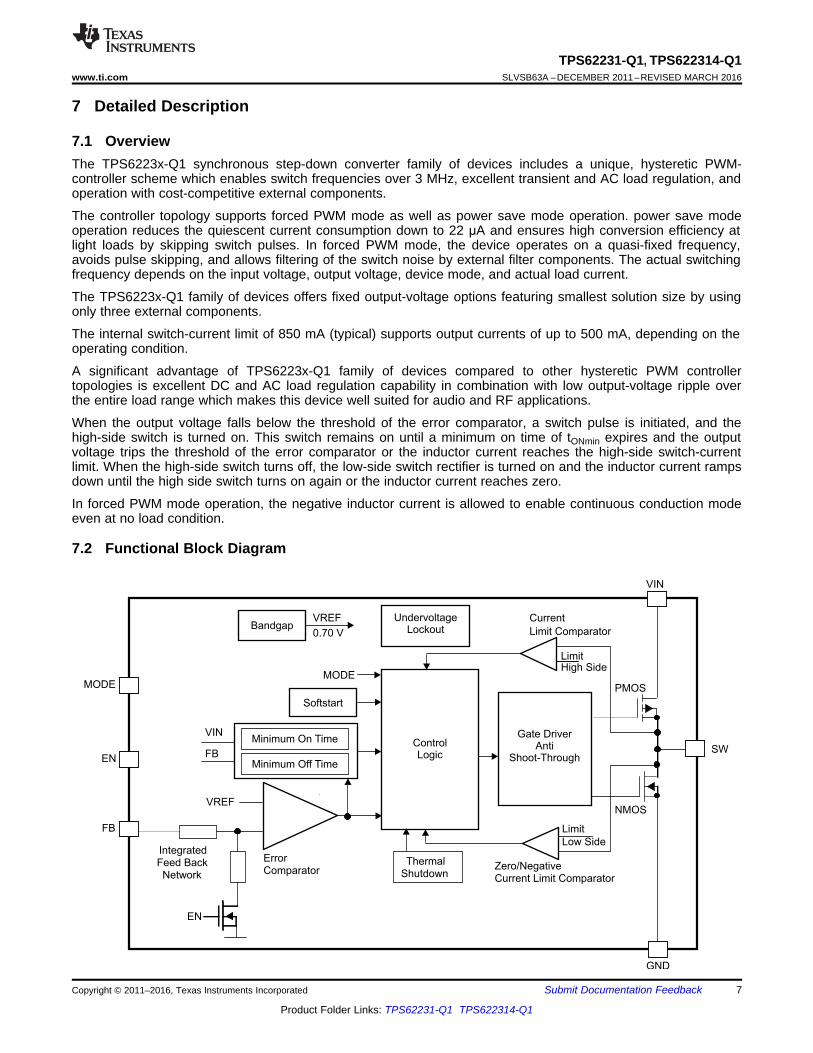
Gate DriverAnti
Shoot-Through
Current
Limit Comparator
SW
Softstart
BandgapUndervoltage
Lockout
LimitHigh Side
Limit
Low Side
FB
EN
MODE
VIN
GND
Minimum On Time
Minimum Off Time
VIN
EN
IntegratedFeed BackNetwork
VREF
FB
ErrorComparator Zero/Negative
Current Limit Comparator
ControlLogic
PMOS
NMOS
MODE
ThermalShutdown
VREF
0.70 V
7
TPS62231-Q1, TPS622314-Q1www.ti.com SLVSB63A –DECEMBER 2011–REVISED MARCH 2016
Product Folder Links: TPS62231-Q1 TPS622314-Q1
Submit Documentation FeedbackCopyright © 2011–2016, Texas Instruments Incorporated
7 Detailed Description
7.1 OverviewThe TPS6223x-Q1 synchronous step-down converter family of devices includes a unique, hysteretic PWM-controller scheme which enables switch frequencies over 3 MHz, excellent transient and AC load regulation, andoperation with cost-competitive external components.
The controller topology supports forced PWM mode as well as power save mode operation. power save modeoperation reduces the quiescent current consumption down to 22 μA and ensures high conversion efficiency atlight loads by skipping switch pulses. In forced PWM mode, the device operates on a quasi-fixed frequency,avoids pulse skipping, and allows filtering of the switch noise by external filter components. The actual switchingfrequency depends on the input voltage, output voltage, device mode, and actual load current.
The TPS6223x-Q1 family of devices offers fixed output-voltage options featuring smallest solution size by usingonly three external components.
The internal switch-current limit of 850 mA (typical) supports output currents of up to 500 mA, depending on theoperating condition.
A significant advantage of TPS6223x-Q1 family of devices compared to other hysteretic PWM controllertopologies is excellent DC and AC load regulation capability in combination with low output-voltage ripple overthe entire load range which makes this device well suited for audio and RF applications.
When the output voltage falls below the threshold of the error comparator, a switch pulse is initiated, and thehigh-side switch is turned on. This switch remains on until a minimum on time of tONmin expires and the outputvoltage trips the threshold of the error comparator or the inductor current reaches the high-side switch-currentlimit. When the high-side switch turns off, the low-side switch rectifier is turned on and the inductor current rampsdown until the high side switch turns on again or the inductor current reaches zero.
In forced PWM mode operation, the negative inductor current is allowed to enable continuous conduction modeeven at no load condition.
7.2 Functional Block Diagram
OUTONmin
IN
Vt = 260 ns
V´
8
TPS62231-Q1, TPS622314-Q1SLVSB63A –DECEMBER 2011–REVISED MARCH 2016 www.ti.com
Product Folder Links: TPS62231-Q1 TPS622314-Q1
Submit Documentation Feedback Copyright © 2011–2016, Texas Instruments Incorporated
7.3 Feature Description
7.3.1 Undervoltage LockoutThe undervoltage-lockout (UVLO) circuit prevents the device from misoperation at low input voltages. This circuitprevents the converter from turning on the switch or rectifier MOSFET under undefined conditions. TheTPS6223x-Q1 family of devices has an UVLO threshold set to 1.8 V (typical). Fully-functional operation ispermitted for the input voltage down to the falling UVLO-threshold level. The converter starts operation againwhen the input voltage crosses the rising UVLO-threshold level.
7.3.2 Enable and ShutdownThe device starts operation when the EN pin is set high and starts up with the soft-start as previously described.For proper operation, the EN pin must be terminated and must not be left floating.
Pulling the EN pin low forces the device into shutdown, with a shutdown quiescent current of 0.1 μA (typical). Inthis mode, the P and N-channel MOSFETs are turned off, the internal resistor feedback divider is disconnected,and the entire internal-control circuitry is switched off.
The EN input can be used to control power sequencing in a system with various DC-DC converters. The EN pincan be connected to the output of another converter, to drive the EN pin high and getting a sequencing of supplyrails.
7.3.3 Thermal ShutdownAs soon as the junction temperature, TJ, exceeds 150°C (typical), the device goes into thermal shutdown. In thismode, the high-side and low-side MOSFETs are turned off. The device continues operation when the junctiontemperature falls below the thermal shutdown hysteresis.
7.4 Device Functional Modes
7.4.1 Soft StartThe device has an internal soft-start circuit that controls the ramp up of the output voltage and limits the inrushcurrent during start-up. This limits input voltage drops when a battery or a high-impedance power source isconnected to the input of the converter.
The soft-start system generates a monotonic ramp up of the output voltage and reaches the nominal outputvoltage which is typically 100 μs after EN pin was pulled high.
If the output voltage does not reach the target value by this time, such as in the case of heavy load, theconverter then operates in a current limit mode set by the switch-current limits.
The device is able to start into a prebiased output capacitor. The converter starts with the applied bias voltageand ramps the output voltage to the nominal value.
7.4.2 Power Save ModeConnecting the MODE pin to GND enables the automatic PWM mode and power save mode operation. Theconverter operates in quasi-fixed frequency PWM mode at moderate to heavy loads and in the PFM (pulsefrequency modulation) mode during light loads, which maintains high efficiency over a wide-load current range. InPFM mode, the device starts to skip switch pulses and generates only single pulses with an on time of tONmin.The PFM Mode frequency depends on the load current and the external inductor and output capacitor values.The PFM mode of the device is optimized for low output-voltage ripple if small external components are used.Even at low output currents, the PFM frequency is above the audible noise spectrum and makes this operationmode suitable for audio applications.
Use Equation 1 to estimate the on time tONmin.
where• tON = High-side switch on time (ns)• VOUT= Output voltage (V)
( )IN OUT OUT DS(on) LV min = V max + I max R max+ R´
I = 0.5 x IOUT_PFM/PWM LPFMpeak
IN OUTLPFMpeak ONmin
(V V )I = t
L
-
´
9
TPS62231-Q1, TPS622314-Q1www.ti.com SLVSB63A –DECEMBER 2011–REVISED MARCH 2016
Product Folder Links: TPS62231-Q1 TPS622314-Q1
Submit Documentation FeedbackCopyright © 2011–2016, Texas Instruments Incorporated
Device Functional Modes (continued)• VIN= Input voltage (V) (1)
Therefore, use Equation 2 to calculate the approximate peak inductor current in PFM mode.
where• ILPFMpeak = PFM inductor peak current (mA)• L = Inductance (µH) (2)
Use Equation 3 to estimate the transition from PFM into PWM mode and from PWM into PFM.
where• IOUT_PFM/PWM = Output current for transition from PFM to PWM mode and transition from PWM to PFM mode
(mA) (3)
7.4.3 Forced PWM ModePulling the MODE pin high forces the converter to operate in a continuous-conduction PWM mode even at lightload currents. The advantage is that the converter operates with a quasi-fixed frequency that allows simplefiltering of the switching frequency for noise-sensitive applications. In this mode, the efficiency is lower comparedto the power save mode during light loads.
For additional flexibility, switch from power save mode to forced PWM mode during operation. This switchingallows for efficient power management by adjusting the operation of the converter to the specific systemrequirements.
7.4.4 100% Duty-Cycle Low-Dropout OperationThe device starts to enter 100% duty-cycle mode when the input voltage comes close to the nominal outputvoltage. To maintain the output voltage, the high-side switch is turned on 100% for one or more cycles.
With further decreasing VIN, the high-side MOSFET switch is turned on completely. In this case the converteroffers a low input-to-output voltage difference which is particularly useful in battery-powered applications toachieve the longest operation time by taking full advantage of the whole battery voltage range.
Use Equation 4 to calculate the minimum input voltage to maintain regulation which is dependent on the loadcurrent and output voltage.
where• VOUTmax = nominal output voltage plus maximum output-voltage tolerance• IOUTmax = maximum output current plus inductor ripple current• RDS(on)max = maximum P-channel switch RDSon• RL = DC resistance of the inductor (4)
7.4.5 Short-Circuit ProtectionThe device integrates a high-side and low-side MOSFET current limit to protect the device against heavy load orshort circuit. The current in the switches is monitored by current-limit comparators. When the current in the P-channel MOSFET reaches the current limit, the P-channel MOSFET is turned off and the N-channel MOSFET isturned on to ramp down the current in the inductor. The high-side MOSFET switch can only turn on again whenthe current in the low-side MOSFET switch has decreased below the threshold of the current-limit comparator.
L
Vout1
VinI = Vout
L
-
D ´´ ¦
CIN2.2 µF
VIN2.05 V to 6 V
COUT4.7 µF
VOUT1.8 V
L1 µH or 2.2 µHTPS62231-Q1
VIN
EN
MODE
SW
FB
GND
10
TPS62231-Q1, TPS622314-Q1SLVSB63A –DECEMBER 2011–REVISED MARCH 2016 www.ti.com
Product Folder Links: TPS62231-Q1 TPS622314-Q1
Submit Documentation Feedback Copyright © 2011–2016, Texas Instruments Incorporated
8 Application and Implementation
NOTEInformation in the following applications sections is not part of the TI componentspecification, and TI does not warrant its accuracy or completeness. TI’s customers areresponsible for determining suitability of components for their purposes. Customers shouldvalidate and test their design implementation to confirm system functionality.
8.1 Application InformationThe TPS6223x-Q1 family of devices is a high-frequency, synchronous, step-down DC-DC converter providingswitch frequencies up to 3.8 MHz.
8.2 Typical Application
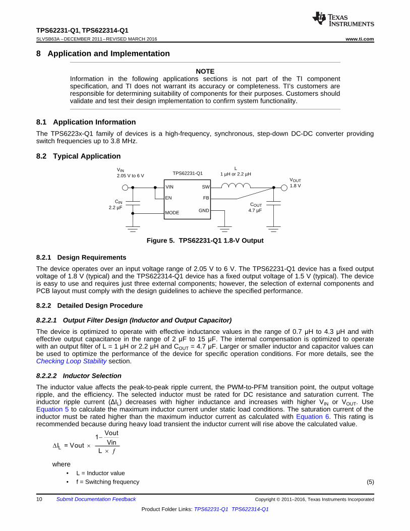
Figure 5. TPS62231-Q1 1.8-V Output
8.2.1 Design RequirementsThe device operates over an input voltage range of 2.05 V to 6 V. The TPS62231-Q1 device has a fixed outputvoltage of 1.8 V (typical) and the TPS622314-Q1 device has a fixed output voltage of 1.5 V (typical). The deviceis easy to use and requires just three external components; however, the selection of external components andPCB layout must comply with the design guidelines to achieve the specified performance.
8.2.2 Detailed Design Procedure
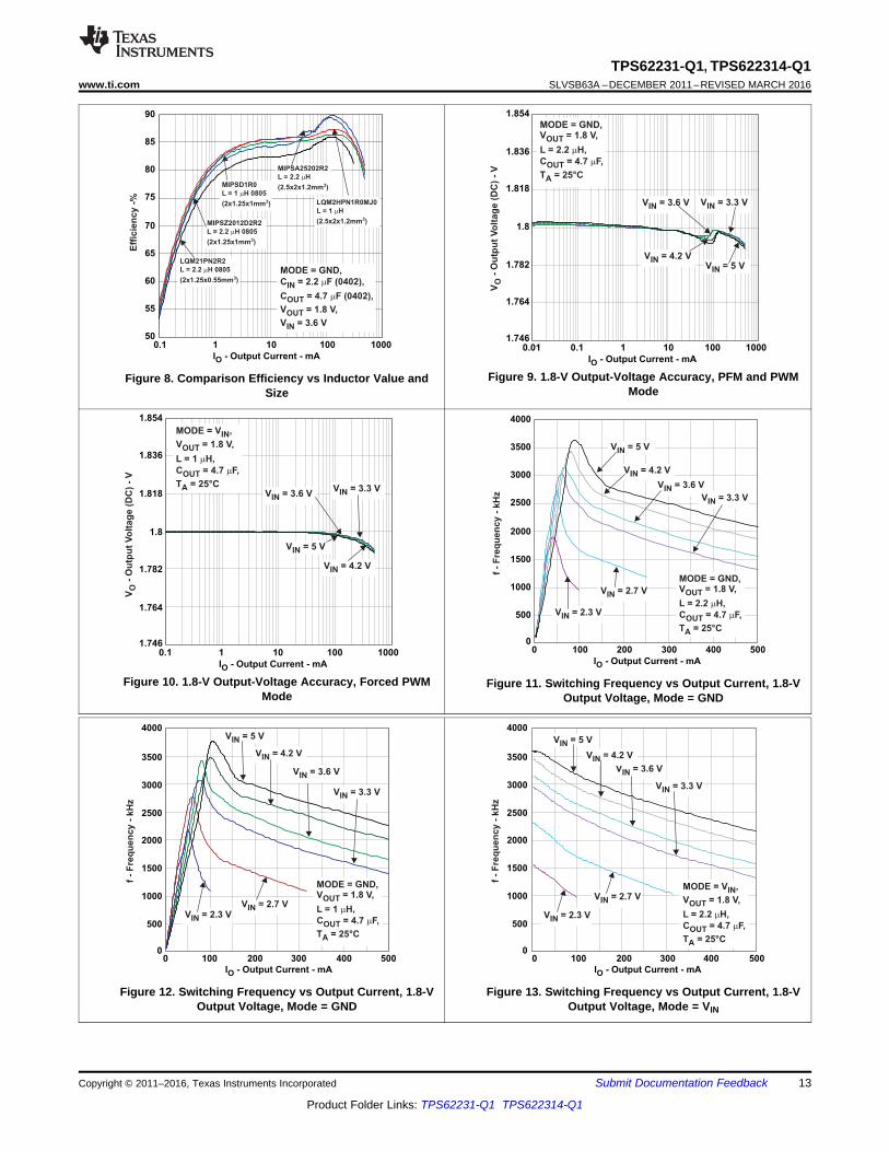
8.2.2.1 Output Filter Design (Inductor and Output Capacitor)The device is optimized to operate with effective inductance values in the range of 0.7 μH to 4.3 μH and witheffective output capacitance in the range of 2 μF to 15 μF. The internal compensation is optimized to operatewith an output filter of L = 1 μH or 2.2 μH and COUT = 4.7 μF. Larger or smaller inductor and capacitor values canbe used to optimize the performance of the device for specific operation conditions. For more details, see theChecking Loop Stability section.
8.2.2.2 Inductor SelectionThe inductor value affects the peak-to-peak ripple current, the PWM-to-PFM transition point, the output voltageripple, and the efficiency. The selected inductor must be rated for DC resistance and saturation current. Theinductor ripple current (ΔIL) decreases with higher inductance and increases with higher VIN or VOUT. UseEquation 5 to calculate the maximum inductor current under static load conditions. The saturation current of theinductor must be rated higher than the maximum inductor current as calculated with Equation 6. This rating isrecommended because during heavy load transient the inductor current will rise above the calculated value.
where• L = Inductor value• f = Switching frequency (5)
LLmax outmax
II = I +
2
D
11
TPS62231-Q1, TPS622314-Q1www.ti.com SLVSB63A –DECEMBER 2011–REVISED MARCH 2016
Product Folder Links: TPS62231-Q1 TPS622314-Q1
Submit Documentation FeedbackCopyright © 2011–2016, Texas Instruments Incorporated
Typical Application (continued)
where• ILmax = Maximum inductor current• ΔIL= Peak-to-peak inductor ripple current (6)
In high-frequency converter applications, the efficiency is essentially affected by the inductor AC resistance(essentially the quality factor) and to a smaller extent by the inductor DCR value. To achieve high efficiencyoperation, use care when selecting inductors featuring a quality factor above 25 at the switching frequency.Increasing the inductor value produces lower RMS currents, but degrades transient response. For a givenphysical inductor size, increased inductance usually results in an inductor with lower saturation current.
The total losses of the coil consist of both the losses in the DC resistance, R(DC), and the following frequency-dependent components:• The losses in the core material (magnetic hysteresis loss, especially at high switching frequencies)• Additional losses in the conductor from the skin effect (current displacement at high frequencies)• Magnetic field losses of the neighboring windings (proximity effect)• Radiation losses
Table 1 lists the inductor series from different suppliers that have been used with the TPS6223x-Q1 converters.These components must be verified and validated to determine whether the component is suitable for the endapplication.
Table 1. List of inductorsINDUCTANCE
(μH)DIMENSIONS
(mm3) INDUCTOR TYPE SUPPLIER
1 2.5 × 2 × 1.2 LQM2HPN1R0MJ0 Murata2.2 2 × 1.2 × 0.55 LQM21PN2R2 Murata
1 or 2.2 2 × 1.2 × 1 KSLI2012 series Hitachi Metal
8.2.2.3 Output Capacitor SelectionThe unique hysteretic PWM control scheme of the TPS6223x-Q1 device allows the use of tiny ceramiccapacitors. Ceramic capacitors with low ESR values have the lowest output voltage ripple and arerecommended. The output capacitor requires either an X7R or X5R dielectric. Y5V and Z5U dielectric capacitors,aside from their wide variation in capacitance over temperature, become resistive at high frequencies.
At light load currents the converter operate in power save mode and the output voltage ripple is dependent onthe output capacitor value and the PFM peak inductor current. Higher output capacitor values minimize thevoltage ripple in PFM Mode and tighten DC output accuracy in PFM Mode.
8.2.2.4 Input Capacitor SelectionBecause of the nature of the buck converter having a pulsating input current, a low-ESR input capacitor isrequired for best input voltage filtering and minimizing the interference with other circuits caused by high inputvoltage spikes. For most applications a 2.2-μF to 4.7-μF ceramic capacitor is recommended. The input capacitorcan be increased without any limit for better input voltage filtering. Because a ceramic capacitor loses up to 80%of the initial capacitance at 5 V, TI recommends using 4.7-μF input capacitors for input voltages greater than 4.5V.
Take care when using only small ceramic input capacitors. When a ceramic capacitor is used at the input and thepower is being supplied through long wires, such as from a wall adapter, a load step at the output or VIN step onthe input can induce ringing at the VIN pin. This ringing can couple to the output and be mistaken as loopinstability or could even damage the part by exceeding the maximum ratings.
Table 2 lists some tested input and output capacitors. These components must be verified and validated todetermine whether the component is suitable for the end application.
0
10
20
30
40
50
60
70
80
90
100
Eff
icie
nc
y -
%
0.1 1 10 100 1000
I - Output Current - mAO
V = 5 VIN
V = 2.7 VIN
V = 3.6 VIN
V = 4.2 VIN
MODE = GND,V = 1.8 V,
L = 2.2 H (MIPSA25202R2),
C = 4.7 F
OUT
OUT
m
m
V = 3.3 VIN
V = 2.3 VIN
0
10
20
30
40
50
60
70
80
90
100
Eff
icie
nc
y -
%
1 10 100 1000
I - Output Current - mAO
MODE = V ,
V = 1.8 V,
L = 2.2 H (MIPSA25202R2),
C = 4.7 F
IN
OUT
OUT
m
m
V = 5 VIN
V = 2.3 VIN
V = 3.6 VIN
V = 4.2 VIN
V = 2.7 VIN
V = 3.3 VIN
12
TPS62231-Q1, TPS622314-Q1SLVSB63A –DECEMBER 2011–REVISED MARCH 2016 www.ti.com
Product Folder Links: TPS62231-Q1 TPS622314-Q1
Submit Documentation Feedback Copyright © 2011–2016, Texas Instruments Incorporated
Table 2. List of CapacitorCAPACITANCE (μF) SIZE CAPACITOR TYPE SUPPLIER
2.2 0402 GRM155R60J225 Murata4.7 0402 AMK105BJ475MV Taiyo Yuden4.7 0402 GRM155R60J475 Murata4.7 0402 CL05A475MQ5NRNC Samsung4.7 0603 GRM188R60J475 Murata
8.2.2.5 Checking Loop StabilityThe first step of circuit and stability evaluation is to look at the following signals from a steady-state perspective:• Switching node, SW• Inductor current, IL• Output ripple voltage, VOUT(AC)
These signals are the basic signals that must be measured when evaluating a switching converter. When theswitching waveform shows large duty-cycle jitter or the output voltage or inductor current shows oscillations, theregulation loop may be unstable. This is often a result of board layout, L-C combination, or both.
As a next step in the evaluation of the regulation loop, the load transient response is tested. The time betweenthe application of the load transient and the turnon of the P-channel MOSFET, the output capacitor must supplyall of the current required by the load. VOUT immediately shifts by an amount equal to ΔI(LOAD) × ESR, where ESRis the effective series resistance of COUT. ΔI(LOAD) begins to charge or discharge CO generating a feedback errorsignal used by the regulator to return VOUT to the steady-state value. The results are most easily interpretedwhen the device operates in PWM mode.
During this recovery time, VOUT can be monitored for settling time, overshoot, or ringing that helps judge thestability of the converter. Without any ringing, the loop has usually more than 45° of phase margin.
Because the damping factor of the circuitry is directly related to several resistive parameters (for example,MOSFET rDS(on)) that are temperature dependant, the loop stability analysis must occur over the input voltagerange, load current range, and temperature range.
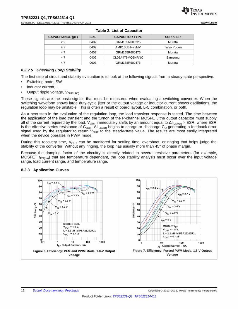
8.2.3 Application Curves
Figure 6. Efficiency: PFM and PWM Mode, 1.8-V OutputVoltage
Figure 7. Efficiency: Forced PWM Mode, 1.8-V OutputVoltage
0 100 200 300 400 500
I - Output Current - mAO
0
500
1000
1500
2000
2500
3000
3500
4000
f -
Fre
qu
en
cy
- k
Hz
MODE = GND,V = 1.8 V,
L = 1 H,
C = 4.7 F,
T = 25°C
OUT
OUT
A
m
m
V = 5 VIN
V = 2.3 VIN
V = 3.6 VIN
V = 4.2 VIN
V = 2.7 VIN
V = 3.3 VIN
V = 5 VIN
V = 2.3 VIN
V = 3.6 VIN
V = 4.2 VIN
V = 2.7 VIN
V = 3.3 VIN
0 100 200 300 400 500
I - Output Current - mAO
MODE = V ,
V = 1.8 V,
L = 2.2 H,
C = 4.7 F,
T = 25°C
IN
OUT
OUT
A
m
m
0
500
1000
1500
2000
2500
3000
3500
4000
f -
Fre
qu
en
cy
- k
Hz
0
500
1000
1500
2000
2500
3000
3500
4000
0 100 200 300 400 500
V = 5 VIN
V = 2.3 VIN
V = 3.6 VIN
V = 4.2 VIN
V = 2.7 VIN
V = 3.3 VIN
I - Output Current - mAO
f -
Fre
qu
en
cy
- k
Hz
MODE = GND,V = 1.8 V,
L = 2.2 H,
C = 4.7 F,
T = 25°C
OUT
OUT
A
m
m
1.746
1.764
1.782
1.8
1.818
1.836
1.854
V = 5 VIN
V = 3.6 VIN
V = 4.2 VIN
MODE = V ,
V = 1.8 V,
L = 1 H,
C = 4.7 F,
T = 25°C
IN
OUT
OUT
A
m
m
0.1 1 10 100 1000
I - Output Current - mAO
V = 3.3 VIN
V-
Ou
tpu
t V
olt
ag
e (
DC
) -
VO
50
55
60
65
70
75
80
85
90
Eff
icie
nc
y -
%
0.1 1 10 100 1000
I - Output Current - mAO
LQM21PN2R2
L = 2.2 H 0805
(2x1.25x0.55mm )
m
3
MIPSZ2012D2R2
L = 2.2 H 0805
(2x1.25x1mm )
m
3
MIPSD1R0
L = 1 H 0805
(2x1.25x1mm )
m
3 LQM2HPN1R0MJ0
L = 1 H
(2.5x2x1.2mm )
m
3
MODE = GND,
C = 2.2 F (0402),
C = 4.7 F (0402),
V = 1.8 V,
V = 3.6 V
IN
OUT
OUT
IN
m
m
MIPSA25202R2
L = 2.2 H
(2.5x2x1.2mm )
m
3
1.746
1.764
1.782
1.8
1.818
1.836
1.854
0.1 1 10 100 1000
I - Output Current - mAO
V = 5 VIN
V = 3.6 VIN
V = 4.2 VIN
MODE = GND,V = 1.8 V,
L = 2.2 H,
C = 4.7 F,
T = 25°C
OUT
OUT
A
m
m
0.01
V = 3.3 VIN
V-
Ou
tpu
t V
olt
ag
e (
DC
) -
VO
13
TPS62231-Q1, TPS622314-Q1www.ti.com SLVSB63A –DECEMBER 2011–REVISED MARCH 2016
Product Folder Links: TPS62231-Q1 TPS622314-Q1
Submit Documentation FeedbackCopyright © 2011–2016, Texas Instruments Incorporated
Figure 8. Comparison Efficiency vs Inductor Value andSize
Figure 9. 1.8-V Output-Voltage Accuracy, PFM and PWMMode
Figure 10. 1.8-V Output-Voltage Accuracy, Forced PWMMode
Figure 11. Switching Frequency vs Output Current, 1.8-VOutput Voltage, Mode = GND
Figure 12. Switching Frequency vs Output Current, 1.8-VOutput Voltage, Mode = GND
Figure 13. Switching Frequency vs Output Current, 1.8-VOutput Voltage, Mode = VIN
V = 1.8 V
20 mV/divOUT
t - Time - 1 ms/div
MODE: 0 V to 3.6 V2 V/div
I
200 mA/divCOIL
V
2 V/divSW
PFM Mode Operation
Forced PWMMode Operation
C = 4.7 F
L = 1 H
V = 3.6 V,IN
OUT m
m
I = 10 mAOUT
V = 1.8 V
50 mV/divOUT
I = 5 mA to 150 mA, 50 kHz
sinusoidal 100 mA/divOUT
I
200 mA/divL
V = 3.6 V
C = 4.7 F
L = 2.2 H
MODE = GND
IN
OUT m
m
t - Time - 4 ms/div
V = 1.8 V
20 mV/div
OUTC = 4.7 F
L = 2.2 H
MODE = GND
OUTm
m
I = 50 mAOUT
t - Time - 10 ms/div
V = 3.6 V to 4.2 V
200 mV/div
IN
V = 1.8 V
20 mV/div
OUTC = 4.7 F
L = 2.2 H
MODE = V
OUT
IN
m
m
I = 50 mAOUT
t - Time - 100 ms/div
V = 3.6 V to 4.2 V
200 mV/div
IN
0
10
20
30
40
50
60
70
80
90
100
10 100 1k 10k 100k 1M
PS
RR
- P
ow
er
Su
pp
ly R
eje
cti
on
Rati
o -
dB
f - Frequency - kHz
I = 50 mA,
MODE = 0,forced PWM
OUT
I = 50 mA,
MODE = 1,PFM/PWM
OUT
I = 150 mA,
PWM ModeOUT
V = 3.6 V,
V = 1.8 V,
C = 2.2 F,
C = 4.7 F,
IN
OUT
IN
OUT
m
m
L = 2.2 Hm0
5
10
15
20
25
30
0 50 100 150 200 250 300 350 400 450 500
I - Output Current - mAO
V-
Pe
ak
-to
-Pe
ak
Ou
tpu
t V
olt
ag
e -
mV
O(P
P)
V = 3.3 VI
V = 3.6 VI
TPS62231V = 1.8 V,
L = 2.2 H 2012,(MIPSZ2012),
C = 4.7 F 0402
O
O
m
m
V = 4.2 VI
14
TPS62231-Q1, TPS622314-Q1SLVSB63A –DECEMBER 2011–REVISED MARCH 2016 www.ti.com
Product Folder Links: TPS62231-Q1 TPS622314-Q1
Submit Documentation Feedback Copyright © 2011–2016, Texas Instruments Incorporated
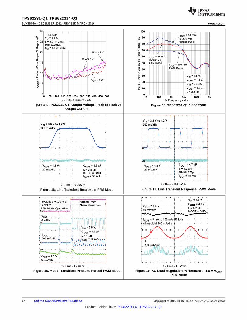
Figure 14. TPS62231-Q1: Output Voltage, Peak-to-Peak vsOutput Current
Figure 15. TPS62231-Q1 1.8-V PSRR
Figure 16. Line Transient Response: PFM Mode Figure 17. Line Transient Response: PWM Mode
Figure 18. Mode Transition: PFM and Forced PWM Mode Figure 19. AC Load-Regulation Performance: 1.8-V VOUT,PFM Mode
f - Frequency
No
ise
Stop10 MHz
400m
1 MHz
10n
300m
200m
100m
700m
500m
1m
800m
900m
V = 2.7V(green)IN
V = 3.6V(blue)IN
V = 3V(red)IN
V = 4.2V(yellow)IN
600m
Start0 Hz
TPS62231MODE = GND,V = 1.8 V,
R
L = 2.2 H,(MIPSZ2012 2R2, Size 2012)
C = 4.7 F (Size 0402)
OUT
LOAD
OUT
= 100R
m
m
Ref Lvl = 1mVRBW 30kHzVBW 30kHzSWT 28ms
f - Frequency
No
ise
Stop40 MHz
400m
4 MHz
10n
300m
200m
100m
700m
500m
1m
800m
900m
600m
Start0 Hz
TPS62231MODE = GND,V = 1.8 V,
R
L = 2.2 H,(MIPSZ2012 2R2, Size 2012)
C = 4.7 F (Size 0402)
OUT
LOAD
OUT
= 12R
m
m
Ref Lvl = 1mVRBW 30kHzVBW 30kHzSWT ´115ms
V = 2.7V(green)IN
V = 3.6V(blue)IN
V = 3V(red)IN
V = 4.2V(yellow)IN
V = 1.8 V
1 V/div
OUT
I
200 mA/div
L
V = 3.6 V
C = 4.7 F
L = 2.2 H
MODE = GND
I = 0 mA
IN
OUT
OUT
m
m
SW 5 V/div
EN 2 V/div
V Pre Bias = 1VOUT
Time Base - 20 s/divm
V = 1.8 V
50 mV/div
OUT
I = 5 mA to 150 mA
100 mA/div
OUT
I
200 mA/div
L
V = 3.6 V
C = 4.7 F
L = 2.2 H
MODE = GND
IN
OUTm
m
t - Time - 10 ms/div
V = 1.8 V
50 mV/div
OUT
I = 5 mA to 150 mA
100 mA/div
OUT
I
200 mA/div
L
V = 3.6 V
C = 4.7 F
L = 2.2 H
MODE = V
IN
OUT
IN
m
m
t - Time - 10 ms/div
15
TPS62231-Q1, TPS622314-Q1www.ti.com SLVSB63A –DECEMBER 2011–REVISED MARCH 2016
Product Folder Links: TPS62231-Q1 TPS622314-Q1
Submit Documentation FeedbackCopyright © 2011–2016, Texas Instruments Incorporated
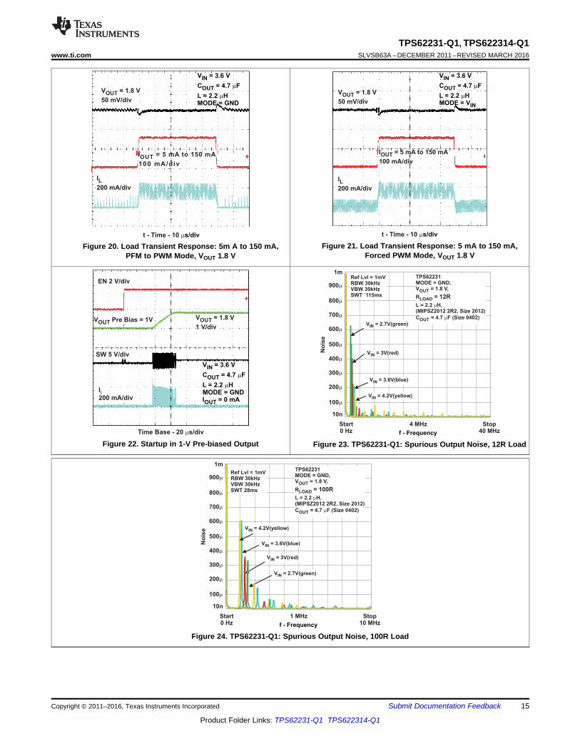
Figure 20. Load Transient Response: 5m A to 150 mA,PFM to PWM Mode, VOUT 1.8 V
Figure 21. Load Transient Response: 5 mA to 150 mA,Forced PWM Mode, VOUT 1.8 V
Figure 22. Startup in 1-V Pre-biased Output Figure 23. TPS62231-Q1: Spurious Output Noise, 12R Load
Figure 24. TPS62231-Q1: Spurious Output Noise, 100R Load
VIN
GND VOUT
C1
C2
L1Total area
is less than
12mm²
16
TPS62231-Q1, TPS622314-Q1SLVSB63A –DECEMBER 2011–REVISED MARCH 2016 www.ti.com
Product Folder Links: TPS62231-Q1 TPS622314-Q1
Submit Documentation Feedback Copyright © 2011–2016, Texas Instruments Incorporated
9 Power Supply RecommendationsThe TPS6223x-Q1 family of devices has no special requirements for the input power supply. The output currentof the input power supply must to be rated according to the supply voltage, output voltage, and output current ofthe TPS6223x-Q1 family of devices.
10 Layout
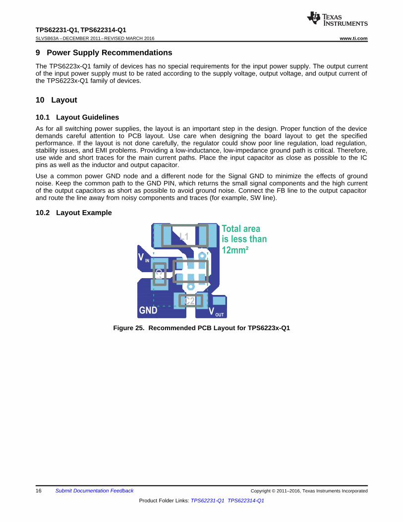
10.1 Layout GuidelinesAs for all switching power supplies, the layout is an important step in the design. Proper function of the devicedemands careful attention to PCB layout. Use care when designing the board layout to get the specifiedperformance. If the layout is not done carefully, the regulator could show poor line regulation, load regulation,stability issues, and EMI problems. Providing a low-inductance, low-impedance ground path is critical. Therefore,use wide and short traces for the main current paths. Place the input capacitor as close as possible to the ICpins as well as the inductor and output capacitor.
Use a common power GND node and a different node for the Signal GND to minimize the effects of groundnoise. Keep the common path to the GND PIN, which returns the small signal components and the high currentof the output capacitors as short as possible to avoid ground noise. Connect the FB line to the output capacitorand route the line away from noisy components and traces (for example, SW line).
10.2 Layout Example
Figure 25. Recommended PCB Layout for TPS6223x-Q1
17
TPS62231-Q1, TPS622314-Q1www.ti.com SLVSB63A –DECEMBER 2011–REVISED MARCH 2016
Product Folder Links: TPS62231-Q1 TPS622314-Q1
Submit Documentation FeedbackCopyright © 2011–2016, Texas Instruments Incorporated
11 Device and Documentation Support
11.1 Device Support
11.1.1 Third-Party Products DisclaimerTI'S PUBLICATION OF INFORMATION REGARDING THIRD-PARTY PRODUCTS OR SERVICES DOES NOTCONSTITUTE AN ENDORSEMENT REGARDING THE SUITABILITY OF SUCH PRODUCTS OR SERVICESOR A WARRANTY, REPRESENTATION OR ENDORSEMENT OF SUCH PRODUCTS OR SERVICES, EITHERALONE OR IN COMBINATION WITH ANY TI PRODUCT OR SERVICE.
11.2 Documentation Support
11.2.1 Related DocumentationFor related documentation see the following:• Basic Calculation of a Buck Converter's Power Stage, SLVA477• QFN/SON PCB Attachment, SLUA271• Performing Accurate PFM Mode Efficiency Measurements, SLVA236
11.3 Related LinksThe table below lists quick access links. Categories include technical documents, support and communityresources, tools and software, and quick access to sample or buy.
Table 3. Related Links
PARTS PRODUCT FOLDER SAMPLE & BUY TECHNICALDOCUMENTS
TOOLS &SOFTWARE
SUPPORT &COMMUNITY
TPS62231-Q1 Click here Click here Click here Click here Click hereTPS622314-Q1 Click here Click here Click here Click here Click here
11.4 Community ResourceThe following links connect to TI community resources. Linked contents are provided "AS IS" by the respectivecontributors. They do not constitute TI specifications and do not necessarily reflect TI's views; see TI's Terms ofUse.
TI E2E™ Online Community TI's Engineer-to-Engineer (E2E) Community. Created to foster collaborationamong engineers. At e2e.ti.com, you can ask questions, share knowledge, explore ideas and helpsolve problems with fellow engineers.
Design Support TI's Design Support Quickly find helpful E2E forums along with design support tools andcontact information for technical support.
11.5 TrademarksE2E is a trademark of Texas Instruments.All other trademarks are the property of their respective owners.
11.6 Electrostatic Discharge CautionThese devices have limited built-in ESD protection. The leads should be shorted together or the device placed in conductive foamduring storage or handling to prevent electrostatic damage to the MOS gates.
11.7 GlossarySLYZ022 — TI Glossary.
This glossary lists and explains terms, acronyms, and definitions.
18
TPS62231-Q1, TPS622314-Q1SLVSB63A –DECEMBER 2011–REVISED MARCH 2016 www.ti.com
Product Folder Links: TPS62231-Q1 TPS622314-Q1
Submit Documentation Feedback Copyright © 2011–2016, Texas Instruments Incorporated
12 Mechanical, Packaging, and Orderable InformationThe following pages include mechanical, packaging, and orderable information. This information is the mostcurrent data available for the designated devices. This data is subject to change without notice and revision ofthis document. For browser-based versions of this data sheet, refer to the left-hand navigation.
PACKAGE OPTION ADDENDUM
www.ti.com 22-Jan-2017
Addendum-Page 1
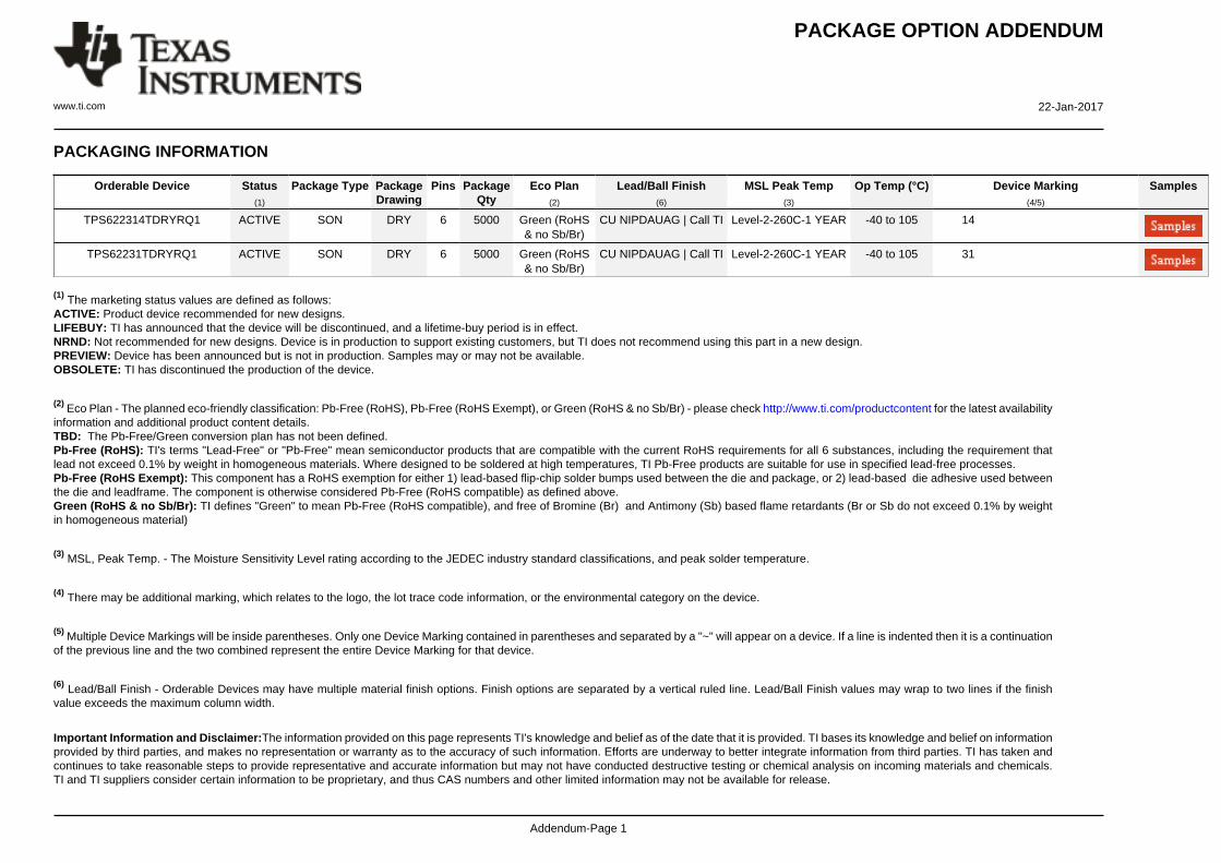
PACKAGING INFORMATION
Orderable Device Status(1)
Package Type PackageDrawing
Pins PackageQty
Eco Plan(2)
Lead/Ball Finish(6)
MSL Peak Temp(3)
Op Temp (°C) Device Marking(4/5)
Samples
TPS622314TDRYRQ1 ACTIVE SON DRY 6 5000 Green (RoHS& no Sb/Br)
CU NIPDAUAG | Call TI Level-2-260C-1 YEAR -40 to 105 14
TPS62231TDRYRQ1 ACTIVE SON DRY 6 5000 Green (RoHS& no Sb/Br)
CU NIPDAUAG | Call TI Level-2-260C-1 YEAR -40 to 105 31
(1) The marketing status values are defined as follows:ACTIVE: Product device recommended for new designs.LIFEBUY: TI has announced that the device will be discontinued, and a lifetime-buy period is in effect.NRND: Not recommended for new designs. Device is in production to support existing customers, but TI does not recommend using this part in a new design.PREVIEW: Device has been announced but is not in production. Samples may or may not be available.OBSOLETE: TI has discontinued the production of the device.
(2) Eco Plan - The planned eco-friendly classification: Pb-Free (RoHS), Pb-Free (RoHS Exempt), or Green (RoHS & no Sb/Br) - please check http://www.ti.com/productcontent for the latest availabilityinformation and additional product content details.TBD: The Pb-Free/Green conversion plan has not been defined.Pb-Free (RoHS): TI's terms "Lead-Free" or "Pb-Free" mean semiconductor products that are compatible with the current RoHS requirements for all 6 substances, including the requirement thatlead not exceed 0.1% by weight in homogeneous materials. Where designed to be soldered at high temperatures, TI Pb-Free products are suitable for use in specified lead-free processes.Pb-Free (RoHS Exempt): This component has a RoHS exemption for either 1) lead-based flip-chip solder bumps used between the die and package, or 2) lead-based die adhesive used betweenthe die and leadframe. The component is otherwise considered Pb-Free (RoHS compatible) as defined above.Green (RoHS & no Sb/Br): TI defines "Green" to mean Pb-Free (RoHS compatible), and free of Bromine (Br) and Antimony (Sb) based flame retardants (Br or Sb do not exceed 0.1% by weightin homogeneous material)
(3) MSL, Peak Temp. - The Moisture Sensitivity Level rating according to the JEDEC industry standard classifications, and peak solder temperature.
(4) There may be additional marking, which relates to the logo, the lot trace code information, or the environmental category on the device.
(5) Multiple Device Markings will be inside parentheses. Only one Device Marking contained in parentheses and separated by a "~" will appear on a device. If a line is indented then it is a continuationof the previous line and the two combined represent the entire Device Marking for that device.
(6) Lead/Ball Finish - Orderable Devices may have multiple material finish options. Finish options are separated by a vertical ruled line. Lead/Ball Finish values may wrap to two lines if the finishvalue exceeds the maximum column width.
Important Information and Disclaimer:The information provided on this page represents TI's knowledge and belief as of the date that it is provided. TI bases its knowledge and belief on informationprovided by third parties, and makes no representation or warranty as to the accuracy of such information. Efforts are underway to better integrate information from third parties. TI has taken andcontinues to take reasonable steps to provide representative and accurate information but may not have conducted destructive testing or chemical analysis on incoming materials and chemicals.TI and TI suppliers consider certain information to be proprietary, and thus CAS numbers and other limited information may not be available for release.
PACKAGE OPTION ADDENDUM
www.ti.com 22-Jan-2017
Addendum-Page 2
In no event shall TI's liability arising out of such information exceed the total purchase price of the TI part(s) at issue in this document sold by TI to Customer on an annual basis.
TAPE AND REEL INFORMATION
*All dimensions are nominal
Device PackageType
PackageDrawing
Pins SPQ ReelDiameter
(mm)
ReelWidth
W1 (mm)
A0(mm)
B0(mm)
K0(mm)
P1(mm)
W(mm)
Pin1Quadrant
TPS622314TDRYRQ1 SON DRY 6 5000 179.0 8.4 1.2 1.65 0.7 4.0 8.0 Q1
TPS62231TDRYRQ1 SON DRY 6 5000 179.0 8.4 1.2 1.65 0.7 4.0 8.0 Q1
PACKAGE MATERIALS INFORMATION
www.ti.com 3-Aug-2017
Pack Materials-Page 1
*All dimensions are nominal
Device Package Type Package Drawing Pins SPQ Length (mm) Width (mm) Height (mm)
TPS622314TDRYRQ1 SON DRY 6 5000 195.0 200.0 45.0
TPS62231TDRYRQ1 SON DRY 6 5000 195.0 200.0 45.0
PACKAGE MATERIALS INFORMATION
www.ti.com 3-Aug-2017
Pack Materials-Page 2
GENERIC PACKAGE VIEW
Images above are just a representation of the package family, actual package may vary.Refer to the product data sheet for package details.
DRY 6 USON - 0.6 mm max heightPLASTIC SMALL OUTLINE - NO LEAD
4207181/G
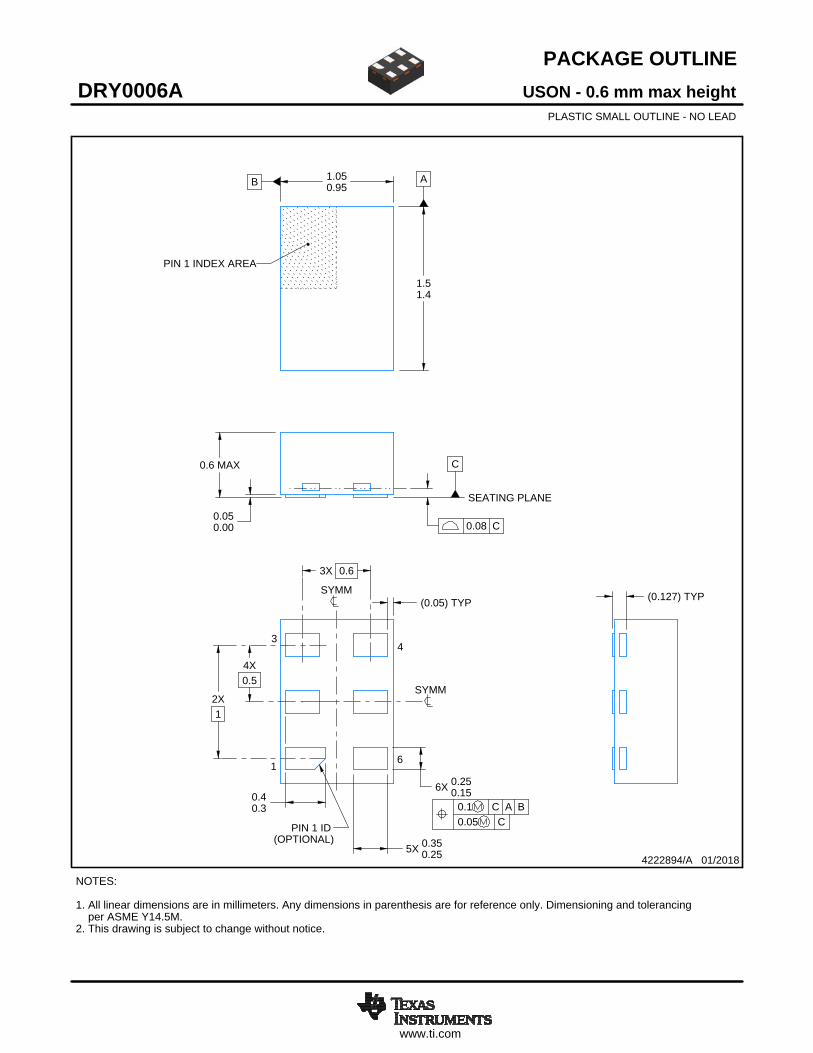
www.ti.com
PACKAGE OUTLINE
C
6X 0.250.15
4X0.5
5X 0.350.25
2X1
0.6 MAX
0.050.00
3X 0.6
0.40.3
B 1.050.95
A
1.51.4
(0.05) TYP (0.127) TYP
4222894/A 01/2018
USON - 0.6 mm max heightDRY0006APLASTIC SMALL OUTLINE - NO LEAD
PIN 1 INDEX AREA
SEATING PLANE
0.08 C
1
34
6
(OPTIONAL)PIN 1 ID
0.1 C A B0.05 C
SYMM
SYMM
NOTES: 1. All linear dimensions are in millimeters. Any dimensions in parenthesis are for reference only. Dimensioning and tolerancing per ASME Y14.5M.2. This drawing is subject to change without notice.
SCALE 8.500
www.ti.com
EXAMPLE BOARD LAYOUT
0.05 MINALL AROUND
0.05 MAXALL AROUND
5X (0.3)
6X (0.2)
4X (0.5)
(0.6)(R0.05) TYP
(0.35)
4222894/A 01/2018
USON - 0.6 mm max heightDRY0006APLASTIC SMALL OUTLINE - NO LEAD
SYMM
1
34
6
SYMM
LAND PATTERN EXAMPLE1:1 RATIO WITH PKG SOLDER PADS
EXPOSED METAL SHOWNSCALE:40X
NOTES: (continued) 3. For more information, see QFN/SON PCB application report in literature No. SLUA271 (www.ti.com/lit/slua271).
METALSOLDER MASKOPENING
SOLDER MASK DETAILS
NON SOLDER MASKDEFINED
EXPOSEDMETAL
SOLDER MASKOPENING
METAL UNDERSOLDER MASK
SOLDER MASKDEFINED
(PREFERRED)
EXPOSEDMETAL
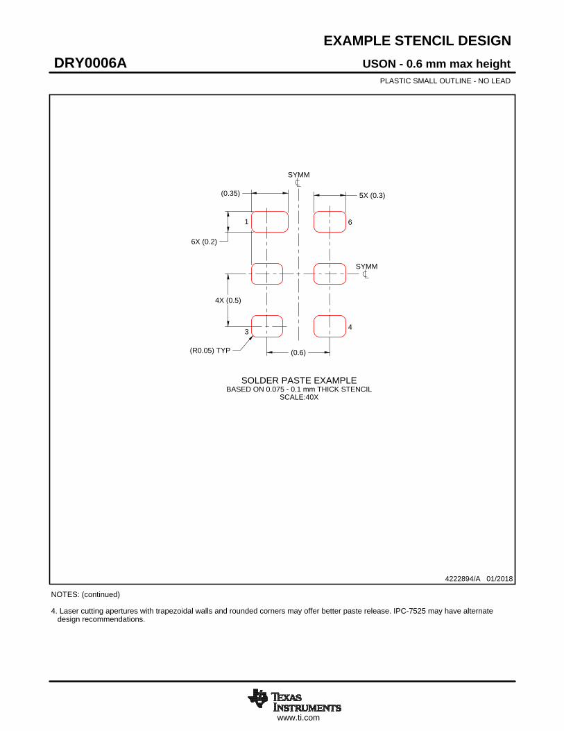
www.ti.com
EXAMPLE STENCIL DESIGN
5X (0.3)
6X (0.2)
4X (0.5)
(0.6)(R0.05) TYP
(0.35)
4222894/A 01/2018
USON - 0.6 mm max heightDRY0006APLASTIC SMALL OUTLINE - NO LEAD
NOTES: (continued) 4. Laser cutting apertures with trapezoidal walls and rounded corners may offer better paste release. IPC-7525 may have alternate design recommendations.
SOLDER PASTE EXAMPLEBASED ON 0.075 - 0.1 mm THICK STENCIL
SCALE:40X
SYMM
1
3 4
6
SYMM
IMPORTANT NOTICE
Texas Instruments Incorporated (TI) reserves the right to make corrections, enhancements, improvements and other changes to itssemiconductor products and services per JESD46, latest issue, and to discontinue any product or service per JESD48, latest issue. Buyersshould obtain the latest relevant information before placing orders and should verify that such information is current and complete.TI’s published terms of sale for semiconductor products (http://www.ti.com/sc/docs/stdterms.htm) apply to the sale of packaged integratedcircuit products that TI has qualified and released to market. Additional terms may apply to the use or sale of other types of TI products andservices.Reproduction of significant portions of TI information in TI data sheets is permissible only if reproduction is without alteration and isaccompanied by all associated warranties, conditions, limitations, and notices. TI is not responsible or liable for such reproduceddocumentation. Information of third parties may be subject to additional restrictions. Resale of TI products or services with statementsdifferent from or beyond the parameters stated by TI for that product or service voids all express and any implied warranties for theassociated TI product or service and is an unfair and deceptive business practice. TI is not responsible or liable for any such statements.Buyers and others who are developing systems that incorporate TI products (collectively, “Designers”) understand and agree that Designersremain responsible for using their independent analysis, evaluation and judgment in designing their applications and that Designers havefull and exclusive responsibility to assure the safety of Designers' applications and compliance of their applications (and of all TI productsused in or for Designers’ applications) with all applicable regulations, laws and other applicable requirements. Designer represents that, withrespect to their applications, Designer has all the necessary expertise to create and implement safeguards that (1) anticipate dangerousconsequences of failures, (2) monitor failures and their consequences, and (3) lessen the likelihood of failures that might cause harm andtake appropriate actions. Designer agrees that prior to using or distributing any applications that include TI products, Designer willthoroughly test such applications and the functionality of such TI products as used in such applications.TI’s provision of technical, application or other design advice, quality characterization, reliability data or other services or information,including, but not limited to, reference designs and materials relating to evaluation modules, (collectively, “TI Resources”) are intended toassist designers who are developing applications that incorporate TI products; by downloading, accessing or using TI Resources in anyway, Designer (individually or, if Designer is acting on behalf of a company, Designer’s company) agrees to use any particular TI Resourcesolely for this purpose and subject to the terms of this Notice.TI’s provision of TI Resources does not expand or otherwise alter TI’s applicable published warranties or warranty disclaimers for TIproducts, and no additional obligations or liabilities arise from TI providing such TI Resources. TI reserves the right to make corrections,enhancements, improvements and other changes to its TI Resources. TI has not conducted any testing other than that specificallydescribed in the published documentation for a particular TI Resource.Designer is authorized to use, copy and modify any individual TI Resource only in connection with the development of applications thatinclude the TI product(s) identified in such TI Resource. NO OTHER LICENSE, EXPRESS OR IMPLIED, BY ESTOPPEL OR OTHERWISETO ANY OTHER TI INTELLECTUAL PROPERTY RIGHT, AND NO LICENSE TO ANY TECHNOLOGY OR INTELLECTUAL PROPERTYRIGHT OF TI OR ANY THIRD PARTY IS GRANTED HEREIN, including but not limited to any patent right, copyright, mask work right, orother intellectual property right relating to any combination, machine, or process in which TI products or services are used. Informationregarding or referencing third-party products or services does not constitute a license to use such products or services, or a warranty orendorsement thereof. Use of TI Resources may require a license from a third party under the patents or other intellectual property of thethird party, or a license from TI under the patents or other intellectual property of TI.TI RESOURCES ARE PROVIDED “AS IS” AND WITH ALL FAULTS. TI DISCLAIMS ALL OTHER WARRANTIES ORREPRESENTATIONS, EXPRESS OR IMPLIED, REGARDING RESOURCES OR USE THEREOF, INCLUDING BUT NOT LIMITED TOACCURACY OR COMPLETENESS, TITLE, ANY EPIDEMIC FAILURE WARRANTY AND ANY IMPLIED WARRANTIES OFMERCHANTABILITY, FITNESS FOR A PARTICULAR PURPOSE, AND NON-INFRINGEMENT OF ANY THIRD PARTY INTELLECTUALPROPERTY RIGHTS. TI SHALL NOT BE LIABLE FOR AND SHALL NOT DEFEND OR INDEMNIFY DESIGNER AGAINST ANY CLAIM,INCLUDING BUT NOT LIMITED TO ANY INFRINGEMENT CLAIM THAT RELATES TO OR IS BASED ON ANY COMBINATION OFPRODUCTS EVEN IF DESCRIBED IN TI RESOURCES OR OTHERWISE. IN NO EVENT SHALL TI BE LIABLE FOR ANY ACTUAL,DIRECT, SPECIAL, COLLATERAL, INDIRECT, PUNITIVE, INCIDENTAL, CONSEQUENTIAL OR EXEMPLARY DAMAGES INCONNECTION WITH OR ARISING OUT OF TI RESOURCES OR USE THEREOF, AND REGARDLESS OF WHETHER TI HAS BEENADVISED OF THE POSSIBILITY OF SUCH DAMAGES.Unless TI has explicitly designated an individual product as meeting the requirements of a particular industry standard (e.g., ISO/TS 16949and ISO 26262), TI is not responsible for any failure to meet such industry standard requirements.Where TI specifically promotes products as facilitating functional safety or as compliant with industry functional safety standards, suchproducts are intended to help enable customers to design and create their own applications that meet applicable functional safety standardsand requirements. Using products in an application does not by itself establish any safety features in the application. Designers mustensure compliance with safety-related requirements and standards applicable to their applications. Designer may not use any TI products inlife-critical medical equipment unless authorized officers of the parties have executed a special contract specifically governing such use.Life-critical medical equipment is medical equipment where failure of such equipment would cause serious bodily injury or death (e.g., lifesupport, pacemakers, defibrillators, heart pumps, neurostimulators, and implantables). Such equipment includes, without limitation, allmedical devices identified by the U.S. Food and Drug Administration as Class III devices and equivalent classifications outside the U.S.TI may expressly designate certain products as completing a particular qualification (e.g., Q100, Military Grade, or Enhanced Product).Designers agree that it has the necessary expertise to select the product with the appropriate qualification designation for their applicationsand that proper product selection is at Designers’ own risk. Designers are solely responsible for compliance with all legal and regulatoryrequirements in connection with such selection.Designer will fully indemnify TI and its representatives against any damages, costs, losses, and/or liabilities arising out of Designer’s non-compliance with the terms and provisions of this Notice.
Mailing Address: Texas Instruments, Post Office Box 655303, Dallas, Texas 75265Copyright © 2018, Texas Instruments Incorporated


![SUBMERSIBLE SUMP PUMPS...SUBMERSIBLE SUMP PUMPS BEST ONE TECHNICAL DATA 60Hz 500 EBARA Pumps Europe S.p.A. Rev. G MOTOR DATA Three Phase Three Phase Three Phase [µF][V][µF][V] 110](https://img.pdfslide.net/doc/110x75/60a9122b6c35ec75147c6eec/submersible-sump-pumps-submersible-sump-pumps-best-one-technical-data-60hz-500.jpg)