Embed Size (px)
Citation preview
Output Load (A)
Eff
icie
nc
y
0
20%
40%
60%
80%
100%
10m 100m 1
D001
V IN = 5 V; V OUT = 1.2 VPSM Mode
PWM Mode
LX1
FB1
LX2
FB2
LX3
FB3
VINx
LVIN2
ENx
PGOOD
MODE
SS1
LOUT2
LFB2
PGNDAGND
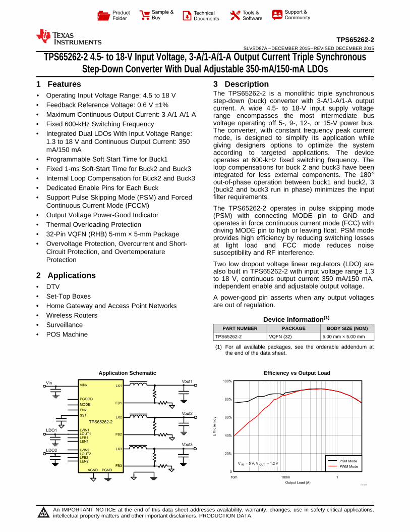
Vin Vout1
Vout3
TPS65262-2
Vout2
LEN2
LVIN1
LOUT1
LFB1
LEN1
LDO1
LDO2
Product
Folder
Sample &Buy
Technical
Documents
Tools &
Software
Support &Community
TPS65262-2SLVSD87A –DECEMBER 2015–REVISED DECEMBER 2015
TPS65262-2 4.5- to 18-V Input Voltage, 3-A/1-A/1-A Output Current Triple SynchronousStep-Down Converter With Dual Adjustable 350-mA/150-mA LDOs
1 Features 3 DescriptionThe TPS65262-2 is a monolithic triple synchronous
1• Operating Input Voltage Range: 4.5 to 18 Vstep-down (buck) converter with 3-A/1-A/1-A output• Feedback Reference Voltage: 0.6 V ±1% current. A wide 4.5- to 18-V input supply voltage
• Maximum Continuous Output Current: 3 A/1 A/1 A range encompasses the most intermediate busvoltage operating off 5-, 9-, 12-, or 15-V power bus.• Fixed 600-kHz Switching FrequencyThe converter, with constant frequency peak current• Integrated Dual LDOs With Input Voltage Range: mode, is designed to simplify its application while1.3 to 18 V and Continuous Output Current: 350 giving designers options to optimize the system
mA/150 mA according to targeted applications. The device• Programmable Soft Start Time for Buck1 operates at 600-kHz fixed switching frequency. The
loop compensations for buck 2 and buck3 have been• Fixed 1-ms Soft-Start Time for Buck2 and Buck3integrated for less external components. The 180°• Internal Loop Compensation for Buck2 and Buck3 out-of-phase operation between buck1 and buck2, 3
• Dedicated Enable Pins for Each Buck (buck2 and buck3 run in phase) minimizes the inputfilter requirements.• Support Pulse Skipping Mode (PSM) and Forced
Continuous Current Mode (FCCM) The TPS65262-2 operates in pulse skipping mode• Output Voltage Power-Good Indicator (PSM) with connecting MODE pin to GND and
operates in force continuous current mode (FCC) with• Thermal Overloading Protectiondriving MODE pin to high or leaving float. PSM mode• 32-Pin VQFN (RHB) 5-mm × 5-mm Package provides high efficiency by reducing switching losses
• Overvoltage Protection, Overcurrent and Short- at light load and FCC mode reduces noiseCircuit Protection, and Overtemperature susceptibility and RF interference.Protection Two low dropout voltage linear regulators (LDO) are
also built in TPS65262-2 with input voltage range 1.32 Applications to 18 V, continuous output current 350 mA/150 mA,independent enable and adjustable output voltage.• DTV
• Set-Top Boxes A power-good pin asserts when any output voltagesare out of regulation.• Home Gateway and Access Point Networks
• Wireless Routers Device Information(1)• Surveillance PART NUMBER PACKAGE BODY SIZE (NOM)• POS Machine TPS65262-2 VQFN (32) 5.00 mm × 5.00 mm
(1) For all available packages, see the orderable addendum atthe end of the data sheet.
Application Schematic Efficiency vs Output Load
1
An IMPORTANT NOTICE at the end of this data sheet addresses availability, warranty, changes, use in safety-critical applications,intellectual property matters and other important disclaimers. PRODUCTION DATA.
TPS65262-2SLVSD87A –DECEMBER 2015–REVISED DECEMBER 2015 www.ti.com
Table of Contents7.3 Feature Description................................................. 131 Features .................................................................. 17.4 Device Functional Modes........................................ 202 Applications ........................................................... 1
8 Application and Implementation ........................ 213 Description ............................................................. 18.1 Application Information............................................ 214 Revision History..................................................... 28.2 Typical Application .................................................. 215 Pin Configuration and Functions ......................... 3
9 Power Supply Recommendations ...................... 316 Specifications......................................................... 510 Layout................................................................... 316.1 Absolute Maximum Ratings ...................................... 5
10.1 Layout Guidelines ................................................. 316.2 ESD Ratings.............................................................. 510.2 Layout Example .................................................... 326.3 Recommended Operating Conditions....................... 5
11 Device and Documentation Support ................. 336.4 Thermal Information .................................................. 511.1 Community Resources.......................................... 336.5 Electrical Characteristics........................................... 611.2 Trademarks ........................................................... 336.6 Typical Characteristics .............................................. 811.3 Electrostatic Discharge Caution............................ 337 Detailed Description ............................................ 1211.4 Glossary ................................................................ 337.1 Overview ................................................................. 12
12 Mechanical, Packaging, and Orderable7.2 Functional Block Diagram ....................................... 13Information ........................................................... 33
4 Revision HistoryNOTE: Page numbers for previous revisions may differ from page numbers in the current version.
Changes from Original (December 2015) to Revision A Page
• Updated device status to production data ............................................................................................................................. 1
2 Submit Documentation Feedback Copyright © 2015, Texas Instruments Incorporated
Product Folder Links: TPS65262-2
1 2 3 4 5 6
9
10
BST1
PGND1
LX1
LEN1
PG
OO
D
LE
N2
SS
1LFB1
VIN1
BST2
LX2
VIN2
VIN3
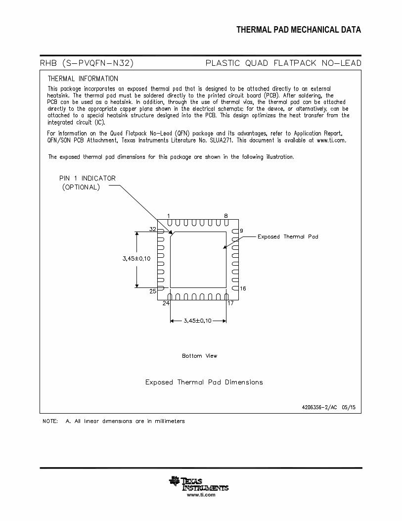
LX3
Thermal Pad
7 8
FB
2
BST3
FB
3
V7V
AG
ND
LO
UT
2
LOUT1
LV
IN2
LF
B2
EN
1
EN
3E
N2
MO
DE
CO
MP
1
PGND3
PGND2
FB
1
LVIN1
11
12
13
14
15
16
1718192021222324
25
26
27
28
29
30
31
32
TPS65262-2www.ti.com SLVSD87A –DECEMBER 2015–REVISED DECEMBER 2015
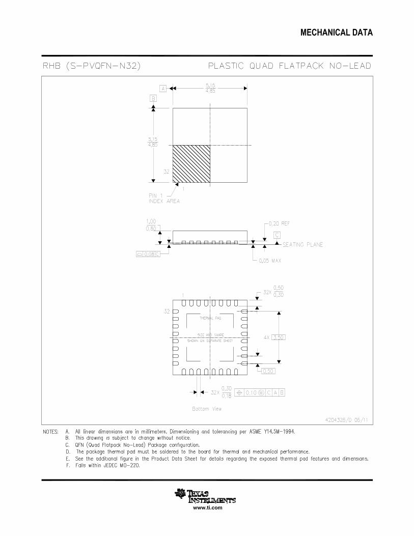
5 Pin Configuration and Functions
32-Pin Plastic VQFNRHB Package
Top View
(There is no electric signal down bonded to thermal pad inside IC. Exposed thermal pad must be soldered to PCB foroptimal thermal performance.)
Pin FunctionsPIN
DESCRIPTIONNAME NO.
Input power supply for LDO2. Connect LVIN2 pin as close as possible to the (+) terminal of an input ceramic capacitorLVIN2 1 (suggest 1 µF).LOUT2 2 LDO2 output. Connect LOUT2 pin as close as possible to the (+) terminal of an output ceramic capacitor (suggest 1 µF).LFB2 3 Feedback Kelvin sensing pin for LDO2 output voltage. Connect this pin to LDO2 resistor divider.LEN2 4 Enable for LDO2. Float to enable.
An open-drain output, asserts low if output voltage of any buck is beyond regulation range due to thermal shutdown,PGOOD 5 overcurrent, undervoltage, or ENx shut down.MODE 6 Switch FCC mode and PSM mode. Pull high or leave floating, FCC mode. Pull low, PSM mode.FB2 7 Feedback Kelvin sensing pin for buck2 output voltage. Connect this pin to buck2 resistor divider.
Enable for buck2. Float to enable. Can use this pin to adjust the input undervoltage lockout of buck2 with a resistorEN2 8 divider.Boot strapped supply to the high side floating gate driver in Buck2. Connect a capacitor (recommend 47 nF) from BST2BST2 9 pin to LX2 pin.Switching node connection to the inductor and bootstrap capacitor for Buck2. The voltage swing at this pin is from aLX2 10 diode voltage below the ground up to VIN2 voltage.Power ground connection of Buck2. Connect PGND2 pin as close as possible to the (–) terminal of VIN2 input ceramicPGND2 11 capacitor.Input power supply for Buck2. Connect VIN2 pin as close as possible to the (+) terminal of an input ceramic capacitorVIN2 12 (suggest 10 µF).Input power supply for Buck3. Connect VIN3 pin as close as possible to the (+) terminal of an input ceramic capacitorVIN3 13 (suggest 10 µF).Power ground connection of Buck3. Connect PGND3 pin as close as possible to the (–) terminal of VIN3 input ceramicPGND3 14 capacitor.Switching node connection to the inductor and bootstrap capacitor for Buck3. The voltage swing at this pin is from aLX3 15 diode voltage below the ground up to VIN3 voltage.
Copyright © 2015, Texas Instruments Incorporated Submit Documentation Feedback 3
Product Folder Links: TPS65262-2
TPS65262-2SLVSD87A –DECEMBER 2015–REVISED DECEMBER 2015 www.ti.com
Pin Functions (continued)PIN
DESCRIPTIONNAME NO.
Boot strapped supply to the high side floating gate driver in Buck3. Connect a capacitor (recommend 47 nF) from BST3BST3 16 pin to LX3 pin.Enable for Buck3. Float to enable. Can use this pin to adjust the input undervoltage lockout of Buck3 with a resistorEN3 17 divider.
FB3 18 Feedback Kelvin sensing pin for buck3 output voltage. Connect this pin to Buck3 resistor divider.Analog ground common to buck controllers and other analog circuits. It must be routed separately from high currentAGND 19 power grounds to the (-) terminal of bypass capacitor of input voltage VIN.
V7V 20 Internal LDO for gate driver and internal controller. Connect a 1-µF capacitor from the pin to power groundError amplifier output and loop compensation pin for Buck1. Connect a series resistor and capacitor to compensate theCOMP1 21 control loop of buck1 with peak current PWM mode.Soft-start and tracking input for Buck1. An internal 5-µA pullup current source is connected to this pin. The soft-start timeSS1 22 can be programmed by connecting a capacitor between this pin and ground.
FB1 23 Feedback Kelvin sensing pin for Buck1 output voltage. Connect this pin to Buck1 resistor divider.Enable for Buck1. Float to enable. Can use this pin to adjust the input undervoltage lockout of Buck1 with a resistorEN1 24 divider.Boot strapped supply to the high side floating gate driver in buck1. Connect a capacitor (recommend 47 nF) from BST1BST1 25 pin to LX1 pin.Switching node connection to the inductor and bootstrap capacitor for buck1. The voltage swing at this pin is from aLX1 26 diode voltage below the ground up to VIN1 voltage.Power ground connection of buck1. Connect PGND1 pin as close as possible to the (–) terminal of VIN1 input ceramicPGND1 27 capacitor.Input power supply for buck1. Connect VIN1 pin as close as possible to the (+) terminal of an input ceramic capacitorVIN1 28 (suggest 10 µF).
LEN1 29 Enable for LDO1. Float to enable.LFB1 30 Feedback Kelvin sensing pin for LDO1 output voltage. Connect this pin to LDO1 resistor divider.LOUT1 31 LDO1 output. Connect LOUT1 pin as close as possible to the (+) terminal of an output ceramic capacitor (suggest 1 µF).
Input power supply for LDO1. Connect LVIN1 pin as close as possible to the (+) terminal of an input ceramic capacitorLVIN1 32 (suggest 1 µF).There is no electric signal down bonded to thermal pad inside IC. Exposed thermal pad must be soldered to PCB forPAD — optimal thermal performance.
4 Submit Documentation Feedback Copyright © 2015, Texas Instruments Incorporated
Product Folder Links: TPS65262-2
TPS65262-2www.ti.com SLVSD87A –DECEMBER 2015–REVISED DECEMBER 2015
6 Specifications
6.1 Absolute Maximum Ratingsover operating free-air temperature range (unless otherwise noted) (operating in a typical application circuit) (1)
MIN MAX UNITVIN1, VIN2, VIN3, LVIN1, LVIN2 –0.3 20LX1, LX2, LX3 (Maximum withstand voltage transient <20 ns) –1.0 20BST1, BST2, BST3 referenced to LX1, LX2, LX3 pins respectively –0.3 7
Voltage MODE, LEN1, LEN2, EN1, EN2, EN3, PGOOD, V7V –0.3 7 VLOUT1, LOUT2 –0.3 7FB1, FB2, FB3, LFB1, LFB2, COMP1 , SS1 –0.3 3.6AGND, PGND1, PGND2, PGND3 –0.3 0.3
TJ Operating junction temperature –40 125 °CTstg Storage temperature –55 150 °C
(1) Stresses beyond those listed under Absolute Maximum Ratings may cause permanent damage to the device. These are stress ratingsonly and functional operation of the device at these or any other conditions beyond those indicated under recommended operatingconditions is not implied. Exposure to absolute-maximum-rated conditions for extended periods may affect device reliability.
6.2 ESD RatingsVALUE UNIT
Human body model (HBM), per ANSI/ESDA/JEDEC JS-001, all pins (1) ±2000ElectrostaticV(ESD) Vdischarge Charged device model (CDM), per JEDEC specification JESD22-C101, all pins (2) ±500
(1) JEDEC document JEP155 states that 500-V HBM allows safe manufacturing with a standard ESD control process. Pins listed as 1 kVmay actually have higher performance.
(2) JEDEC document JEP157 states that 250-V CDM allows safe manufacturing with a standard ESD control process. Pins listed as 250 Vmay actually have higher performance.
6.3 Recommended Operating Conditionsover operating free-air temperature range (unless otherwise noted)
MIN MAX UNITVIN1, VIN2, VIN3, LVIN1, LVIN2 4.5 18LX1, LX2, LX3 (maximum withstand voltage transient <20 ns) –0.8 18BST1, BST2, BST3 referenced to LX1, LX2, LX3 pins respectively –0.1 6.8
Voltage VMODE, LEN1, LEN2, EN1, EN2, EN3, PGOOD, V7V –0.1 6.3FB1, FB2, FB3, LFB1, LFB2, COMP1 , SS1 –0.1 3LOUT1, LOUT2 –0.1 5.5
TJ Operating junction temperature –40 125 °C
6.4 Thermal InformationTPS65262-2
THERMAL METRIC (1) RHB (VQFN) UNIT32 PINS
RθJA Junction-to-ambient thermal resistance 32 °C/WRθJC(top) Junction-to-case (top) thermal resistance 24.2 °C/WRθJB Junction-to-board thermal resistance 6.4 °C/WψJT Junction-to-top characterization parameter 0.2 °C/WψJB Junction-to-board characterization parameter 6.4 °C/WRθJc(bot) Junction-to-case (bottom) thermal resistance 1.3 °C/W
(1) For more information about traditional and new thermal metrics, see the Semiconductor and IC Package Thermal Metrics applicationreport, SPRA953.
Copyright © 2015, Texas Instruments Incorporated Submit Documentation Feedback 5
Product Folder Links: TPS65262-2
TPS65262-2SLVSD87A –DECEMBER 2015–REVISED DECEMBER 2015 www.ti.com
6.5 Electrical CharacteristicsTJ = –40°C to 125°C, typical values are at TJ = 25°C (unless otherwise noted)
PARAMETER TEST CONDITIONS MIN TYP MAX UNIT
INPUT SUPPLY VOLTAGE
VIN Input voltage range 4.5 18 V
VIN rising 4 4.25 4.5V
UVLO VIN undervoltage lockout VIN falling 3.5 3.75 4
Hysteresis 500 mV
IDDSDN Shutdown supply current EN1 = EN2 = EN3 = MODE = LEN1 = LEN2 = 0 V 12 µA
EN1 = EN2 = EN3 = 5V, FB1 = FB2 = FB3 = 0.8 V,IDDQ_NSW 790 µALEN1 = LEN2 = 0 V
EN1 = 5 V, EN2 = EN3 = 0 V, FB1 = 0.8 V,IDDQ_NSW1 340 µALEN1 = LEN2 = 0 VInput quiescent current withoutbuck1/2/3 switching EN2 = 5 V, EN1 = EN3 = 0V, FB2 = 0.8 V,IDDQ_NSW2 370 µALEN1 = LEN2 = 0 V
EN3 = 5 V, EN1 = EN2 = 0 V, FB3 = 0.8 V,IDDQ_NSW3 370 µALEN1 = LEN2 = 0 V
EN1 = EN2 = EN3 = LEN2 = 0 V, LFB1 = 0.8 V, LEN1IDDQ_LDO1 190 µA= 5 VLDO input quiescent current
EN1 = EN2 = EN3 = LEN1 = 0 V, LFB2 = 0.8 V, LEN2IDDQ_LDO2 190 µA= 5 V
V7V V7V LDO output voltage VIN1 = 12 V; V7V load current = 0 A 6.0 6.3 6.6 V
IOCP_V7V V7V LDO current limit 175 mA
FEEDBACK VOLTAGE REFERENCE
VCOMP = 1.2 V, TJ = 25°C 0.595 0.6 0.605 VVFB Feedback voltage
VCOMP = 1.2 V, TJ = –40°C to 125°C 0.594 0.6 0.606 V
IOUT1 = 1.5 A, IOUT2 = 1 A,VLINEREG_Buck Line regulation-DC (1) 0.002 %/VIOUT3 = 1 A, 5 V < VINx < 18 V
VLOADREG_Buck Load regulation-DC (1) VIN = 12 V, IOUTx = (10-100%) × IOUTx_max 0.02 %/A
BUCK1, BUCK2, BUCK3
VENXH EN1/2/3 high level input voltage 1.2 1.27 V
VENXL EN1/2/3 low level input voltage 1.0 1.15 V
IENX EN1/2/3 pullup current ENx = 1 V 3.6 µA
IENX EN1/2/3 pullup current ENx = 1.5 V 6.6 µA
IENhys Hysteresis current 3 µA
ISS1 Buck1 soft start charging current 4.3 5 6.1 µA
TSS2/3 Buck2/3 soft start time 1 ms
TON_MIN Minimum on time 80 100 ns
Gm_EA1/2/3 Error amplifier trans-conductance –2 µA < ICOMPX < 2 µA 300 µS
COMP voltage to inductor currentGm_PS1/2/3 ILX = 0.5 A 7.4 A/VGm(1)
ILIMIT1 Buck1 peak inductor current limit 4.2 5.1 6 A
ILIMITSOURCE1 Buck1 low-side source current limit 4.4 A
ILIMITS1 Buck1 low-side sink current limit 1.3 A
ILIMIT2/3 Buck2/3 peak inductor current limit 1.8 2.4 3 A
ILIMITSOURCE2/3 Buck2/3 low-side source current limit 1.75 A
ILIMITS2/3 Buck2/3 low-side sink current limit 1 A
tHiccup_wait OC wait time (1) 0.5 ms
tHiccup_re Hiccup time before restart (1) 14 ms
Rdson_HS1 Buck1 High-side switch resistance VIN1 = 12 V 100 mΩ
Rdson_LS1 Buck1 low-side switch resistance VIN1 = 12 V 65 mΩ
Rdson_HS2 Buck2 High-side switch resistance VIN1 = 12 V 195 mΩ
Rdson_LS2 Buck2 low-side switch resistance VIN1 = 12 V 145 mΩ
Rdson_HS3 Buck3 High-side switch resistance VIN1 = 12 V 195 mΩ
Rdson_LS3 Buck3 low-side switch resistance VIN1 = 12 V 145 mΩ
(1) Lab validation result.
6 Submit Documentation Feedback Copyright © 2015, Texas Instruments Incorporated
Product Folder Links: TPS65262-2
TPS65262-2www.ti.com SLVSD87A –DECEMBER 2015–REVISED DECEMBER 2015
Electrical Characteristics (continued)TJ = –40°C to 125°C, typical values are at TJ = 25°C (unless otherwise noted)
PARAMETER TEST CONDITIONS MIN TYP MAX UNIT
POWER GOOD, MODE, POWER SEQUENCE
FBx undervoltage falling 92.5%
FBx undervoltage rising 95%Vth_PG Feedback voltage threshold VREF
FBx overvoltage rising 107.5%
FBx overvoltage falling 105%
tDEGLITCH(PG)_F PGOOD falling edge deglitch time 0.19 ms
tRDEGLITCH(PG)_R PGOOD rising edge deglitch time 1 ms
IPG PGOOD pin leakage 0.05 µA
VLOW_PG PGOOD pin low voltage ISINK = 1 mA 0.4 V
VMODEH MODE high level input voltage 1.2 1.27 V
VMODEL MODE low level input voltage 1.0 1.15 V
IMODE MODE pullup current MODE = 1 V 3.6 µA
IMODE MODE pullup current MODE = 1.5 V 6.6 µA
LDO1 AND LDO2
VLENXH LEN1, LEN2 high-level input voltage 1.2 1.27 V
VLENXL LEN1, LEN2 low-level input voltage 1.0 1.15 V
LENx = 1 V 3.6ILENX LEN1, LEN2 pullup current µA
LENx = 1.5 V 6.6
VINLDO1 LDO input voltage range 1.3 18 V
VOUTLDO1 LDO output voltage range load current = 350 mA, VIN = 12 V 1 5.5 V
VLDOFB1 LDO voltage reference load current = 10 mA, VIN = 12 V 0.593 0.6 0.607 V
Imax_LDO1 LDO current limit 350 440 559 mA
IOUT = 20 mA 12 mVVdropout1 LDO dropout voltage
IOUT = 200 mA 120 mV
VOUT = 1.8 V, IOUT = 10 mA, LVIN1 changes from 2 toVLINEREG_LDO1 LDO line regulation-DC (1) 0.002 %/V18 V
VLOADREG_LDO1 LDO load regulation-DC (1) IOUT = 1 mA to 350 mA 0.2 %/A
Vin_LDO1 = 12 V, VOUT = 1.8 V, IOUT = 10 mA,PSRRLDO1 Ripple rejection (1) 56 dBƒ = 10 kHz
VINLDO2 LDO input voltage range 1.3 18 V
VOUTLDO2 LDO output voltage range Load current = 150 mA, VIN = 12 V 1 5.5 V
VLDOFB2 LDO voltage reference Load current = 10 mA, VIN = 12 V 0.593 0.6 0.607 V
Imax_LDO2 LDO current limit 160 230 295 mA
IOUT = 10 mA 12 mVVdropout2 LDO drop out voltage
IOUT = 100 mA 120 mV
VOUT = 1.8 V, IOUT = 10 mA, LVIN1 changes from 2 toVLINEREG_LDO2 LDO line regulation-DC (1) 0.002 %/V18 V
VLOADREG_LDO2 LDO load regulation-DC (1) IOUT = 1 to 150 mA, VIN = 12 V 0.2 %/A
Vin_LDO2 = 12 V, VOUT = 1.8 V, IOUT = 10 mA,PSRRLDO2 Ripple rejection (1) 56 dBƒ = 10 kHz
OSCILLATOR
ƒSW Switching frequency 540 600 670 kHz
THERMAL PROTECTION
TTRIP_OTP Temperature rising 160 °CThermal protection trip point (1)
THYST_OTP Hysteresis 20 °C
Copyright © 2015, Texas Instruments Incorporated Submit Documentation Feedback 7
Product Folder Links: TPS65262-2
3.27
3.28
3.29
3.30
3.31
3.32
3.33
0.0 0.2 0.4 0.6 0.8 1.0
Out
put
Vol
tage
t V
Output Load t A
VIN 5 V
VIN 12 V
C004
1.192
1.194
1.196
1.198
1.200
1.202
1.204
1.206
1.208
4 6 8 10 12 14 16 18
Out
put
Vol
tage
t V
Input Voltage t V
IOUT 0.1 AIOUT 1.5 AIOUT 3 A
C007
1.180
1.185
1.190
1.195
1.200
1.205
1.210
1.215
1.220
0.0 0.5 1.0 1.5 2.0 2.5 3.0
Out
put
Vol
tage
t V
Output Load t A
VIN 5 V
VIN 12 V
C004
1.780
1.785
1.790
1.795
1.800
1.805
1.810
1.815
1.820
0.0 0.2 0.4 0.6 0.8 1.0
Out
put
Vol
tage
t V
Output Load t A
VIN 5 V
VIN 12 V
C004
0%
10%
20%
30%
40%
50%
60%
70%
80%
90%
100%
0.01 0.10 1.00
Effi
cien
cy (
%)
Output Load t A
PSM Mode VOUT 1.2 V
PSM Mode VOUT 3.3 V
PSM Mode VOUT 5 V
C002
0%
10%
20%
30%
40%
50%
60%
70%
80%
90%
100%
0.01 0.10 1.00
Effi
cien
cy (
%)
Output Load t A
PSM Mode VOUT 1.8 V
PSM Mode VOUT 3.3 V
PSM Mode VOUT 5 V
C002
TPS65262-2SLVSD87A –DECEMBER 2015–REVISED DECEMBER 2015 www.ti.com
6.6 Typical CharacteristicsTA = 25°C, VIN = 12 V, VOUT1 = 1.2 V, VOUT2 = 1.8 V, VOUT3 = 3.3 V, ƒSW = 600 kHz (unless otherwise noted)
Figure 1. Buck1 Efficiency Figure 2. Buck2 Efficiency
Figure 3. Buck1, PSM Mode Load Regulation Figure 4. Buck2, PSM Mode Load Regulation
Figure 5. Buck3, PSM Mode Load Regulation Figure 6. Buck1, PSM Mode Line Regulation
8 Submit Documentation Feedback Copyright © 2015, Texas Instruments Incorporated
Product Folder Links: TPS65262-2
1.792
1.794
1.796
1.798
1.800
1.802
1.804
1.806
1.808
2 4 6 8 10 12 14 16 18
Out
put
Vol
tage
t V
Input Voltage t V
IOUT 0.02 AIOUT 0.1 AIOUT 0.2 A
C007
1.792
1.794
1.796
1.798
1.800
1.802
1.804
1.806
1.808
2 4 6 8 10 12 14 16 18
Out
put
Vol
tage
t V
Input Voltage t V
IOUT 0.01 AIOUT 0.05 AIOUT 0.1 A
C007
Output Load - A
Out
put V
olta
ge -
V
0 0.05 0.1 0.15 0.2 0.25 0.3 0.351.78
1.79
1.8
1.81
1.82
D001Output Load - A
Out
put V
olta
ge -
V
0 0.03 0.06 0.09 0.12 0.151.78
1.79
1.8
1.81
1.82
D001
1.792
1.794
1.796
1.798
1.800
1.802
1.804
1.806
1.808
4 6 8 10 12 14 16 18
Out
put
Vol
tage
t V
Input Voltage t V
IOUT 0.1 AIOUT 0.5 AIOUT 1 A
C007
3.280
3.285
3.290
3.295
3.300
3.305
3.310
3.315
3.320
4 6 8 10 12 14 16 18
Out
put
Vol
tage
t V
Input Voltage t V
IOUT 0.1 AIOUT 0.5 AIOUT 1 A
C007
TPS65262-2www.ti.com SLVSD87A –DECEMBER 2015–REVISED DECEMBER 2015
Typical Characteristics (continued)TA = 25°C, VIN = 12 V, VOUT1 = 1.2 V, VOUT2 = 1.8 V, VOUT3 = 3.3 V, ƒSW = 600 kHz (unless otherwise noted)
Figure 7. Buck2, PSM Mode Line Regulation Figure 8. Buck3, PSM Mode Line Regulation
Figure 9. LDO1, Load Regulation, VIN = 3.3 V Figure 10. LDO2, Load Regulation, VIN = 3.3 V
Figure 11. LDO1, Line Regulation Figure 12. LDO2, Line Regulation
Copyright © 2015, Texas Instruments Incorporated Submit Documentation Feedback 9
Product Folder Links: TPS65262-2
5.4
6.0
6.6
7.2
7.8
±50 ±30 ±10 10 30 50 70 90 110 130
EN
Pin
On
Pul
lup
(uA
)
Junction Temperature (C) C014
1.12
1.16
1.20
1.24
1.28
±50 ±30 ±10 10 30 50 70 90 110 130
Pin
Thr
esho
ld R
aisi
ng (
V)
Junction Temperature (C) C014
6
8
10
12
14
16
18
±50 ±30 ±10 10 30 50 70 90 110 130
Shu
tdow
n Q
uies
cent
Cur
rent
(uA
)
Junction Temperature (C) C014
2.4
3.0
3.6
4.2
4.8
±50 ±30 ±10 10 30 50 70 90 110 130
EN
Pin
On
Pul
lup
(uA
)
Junction Temperature (C) C014
0.594
0.596
0.598
0.600
0.602
0.604
0.606
±50 ±30 ±10 10 30 50 70 90 110 130
Vol
tage
Ref
eren
ce (
V)
Junction Temperature (C) C014
560
580
600
620
640
±50 ±30 ±10 10 30 50 70 90 110 130
Osc
illat
or F
eque
ncy
(kH
z)
Junction Temperature (C) C014
TPS65262-2SLVSD87A –DECEMBER 2015–REVISED DECEMBER 2015 www.ti.com
Typical Characteristics (continued)TA = 25°C, VIN = 12 V, VOUT1 = 1.2 V, VOUT2 = 1.8 V, VOUT3 = 3.3 V, ƒSW = 600 kHz (unless otherwise noted)
Figure 13. Voltage Reference vs Temperature Figure 14. Oscillator Frequency vs Temperature
Figure 15. Shutdown Quiescent Current vs Temperature Figure 16. EN Pin Pullup Current vs Temperature, EN = 1 V
Figure 17. EN Pin Pullup Current vs Temperature, EN = 1.5 V Figure 18. EN Pin Threshold Rising vs Temperature
10 Submit Documentation Feedback Copyright © 2015, Texas Instruments Incorporated
Product Folder Links: TPS65262-2
4.7
4.9
5.1
5.3
5.5
±50 ±30 ±10 10 30 50 70 90 110 130
Hig
h S
ide
Cur
rent
Lim
it (A
)
Junction Temperature (C) C014
2.0
2.2
2.4
2.6
2.8
±50 ±30 ±10 10 30 50 70 90 110 130
Hig
h S
ide
Cur
rent
Lim
it (A
)
Junction Temperature (C)
buck2
buck3
C014
1.07
1.11
1.15
1.19
1.23
±50 ±30 ±10 10 30 50 70 90 110 130
Pin
Thr
esho
ld F
allin
g (V
)
Junction Temperature (C) C014
4.2
4.6
5.0
5.4
5.8
±50 ±30 ±10 10 30 50 70 90 110 130
Sof
t Sta
rt C
urre
nt (
mA
)
Junction Temperature (C) C014
TPS65262-2www.ti.com SLVSD87A –DECEMBER 2015–REVISED DECEMBER 2015
Typical Characteristics (continued)TA = 25°C, VIN = 12 V, VOUT1 = 1.2 V, VOUT2 = 1.8 V, VOUT3 = 3.3 V, ƒSW = 600 kHz (unless otherwise noted)
Figure 19. EN Pin Threshold Falling vs Temperature Figure 20. SS Pin Charge Current vs Temperature
Figure 21. Buck1 High-Side Current Limit vs Temperature Figure 22. Buck2, 3 High-Side Current Limit vs Temperature
Copyright © 2015, Texas Instruments Incorporated Submit Documentation Feedback 11
Product Folder Links: TPS65262-2
TPS65262-2SLVSD87A –DECEMBER 2015–REVISED DECEMBER 2015 www.ti.com
7 Detailed Description
7.1 OverviewThe TPS65262-2 is a monolithic triple synchronous step-down (buck) converter with 3-A/1-A/1-A output currents.A wide 4.5- to 18-V input supply voltage range encompasses most intermediate bus voltages operating off 5-, 9-,12-, or 15-V power bus. The feedback voltage reference for each buck is 0.6V. Each buck is independent withdedicated enable, soft-start and loop compensation.
The TPS65262-2 implements a constant frequency, peak current mode control that simplifies external loopcompensation. The switching frequency is fixed 600 kHz. The switching clock of buck1 is 180° out-of-phaseoperation from the clocks of buck2 and buck3 channels to reduce input current ripple, input capacitor size andpower supply induced noise.
The TPS65262-2 has been designed for safe monotonic startup into pre-biased loads. The default start up iswhen VIN is typically 4.5 V. The ENx pin also can be used to adjust the input voltage undervoltage lockout(UVLO) with an external resistor divider. In addition, the ENx pin has an internal 3.6-µA current source, so theEN pin can be floating for automatically powering up the converters.
The TPS65262-2 reduces the external component count by integrating the bootstrap circuit. The bias voltage forthe integrated high-side MOSFET is supplied by a capacitor between the BST and LX pins. A UVLO circuitmonitors the bootstrap capacitor voltage VBST-VLX in each buck. When VBST-VLX voltage drops to thethreshold, LX pin is pulled low to recharge the bootstrap capacitor. The TPS65262-2 can operate at 100% dutycycle as long as the bootstrap capacitor voltage is higher than the BOOT-LX UVLO threshold which is typically2.1 V.
The TPS65262-2 features a PGOOD pin to supervise each output voltage of buck converters. The TPS65262-2has power good comparators with hysteresis, which monitor the output voltages through feedback voltages.When all bucks are in regulation range and power sequence is done, PGOOD is asserted to high.
The SS (soft start/tracking) pin is used to minimize inrush currents during power up. A small value capacitor orresistor divider is coupled to the pin for soft start or voltage tracking.
The TPS65262-2 operates in pulse skipping mode (PSM) with connecting MODE pin to GND and operates inforced continuous current (FCC) mode with driving MODE pin to high or leaving float.
The TPS65262-2 integrates low drop-out voltage linear regulators (LDO) with input voltage from 1.3 to 18 V,independent enable and adjustable outputs, up to 350 mA for LDO1 and 150 mA for LDO2 continuous outputcurrent.
The TPS65262-2 is protected from overload and over temperature fault conditions. The converter minimizesexcessive output overvoltage transients by taking advantage of the power good comparator. When the output isover, the high-side MOSFET is turned off until the internal feedback voltage is lower than 105% of the 0.6-Vreference voltage. The TPS65262-2 implements both high-side MOSFET overload protection and bidirectionallow-side MOSFET overload protections to avoid inductor current runaway. If the over current condition has lastedfor more than the OC wait time (0.5 ms), the converter will shut down and restart after the hiccup time (14 ms).The TPS65262-2 shuts down if the junction temperature is higher than thermal shutdown trip point 160°C. Whenthe junction temperature drops 20°C (typical) below the thermal shutdown trip point, the TPS65262-2 will berestarted under control of the soft-start circuit automatically.
The TPS65262-2 is available in a 32-lead thermally-enhanced VQFN (RHB) package.
12 Submit Documentation Feedback Copyright © 2015, Texas Instruments Incorporated
Product Folder Links: TPS65262-2
2 1
out
0.6R R
V 0.6= ´
-
Vout
FB
R1
R20.6V
COMP
OSC-600kHz
Phase Shift
V7V LDO
Bias
V7V
AGND
FB1
FB2
Over
Temp
EN1(EN2, EN3)
LEN1(LEN2)
State
Machine
FB3
en_buck1
MODE
PGOOD
VIN1
BST1
LX1
PGND1
BUCK1
enable
V7V
VIN
BST
LX
PGND
FB1
VIN
SSSS1
V3V
en_buck1
en_buck2
en_buck3
OT
COMP1
MODE
3uA
1.2V
3.6uA
Comp
vfb
2K 6.3V
3uA
1.2V
3.6uA
6.3V2K
5uA
3uA
1.2V
3.6uA
2K 6.3V
CLK2
CLK3
CLK1
clk1
VIN2
BST2
LX2
PGND2
BUCK2enable
V7V
VIN
BST
LX
PGND
FB2
VIN
en_buck2
MODE
vfb
clk2
en_ldo2
en_ldo1
LDO1enable
LVIN
LOUT
FB
en_ldo1
VINLVIN1
LOUT1
LFB1
LDO2enable
LVIN
LOUT
FB
en_ldo2
LVIN2
LOUT2
LFB2
VIN
VIN3
BST3
LX3
PGND3
BUCK3enable
V7V
VIN
BST
LX
PGND
FB3
VIN
en_buck3
MODE
vfb
clk3
Power
Good
TPS65262-2www.ti.com SLVSD87A –DECEMBER 2015–REVISED DECEMBER 2015
7.2 Functional Block Diagram
7.3 Feature Description
7.3.1 Adjusting the Output VoltageThe output voltage of each buck is set with a resistor divider from the output of buck to the FB pin. TIrecommends to use 1% tolerance or better divider resistors.
Figure 23. Voltage Divider Circuit
(1)
To improve efficiency at light loads consider using larger value resistors. If the values are too high, the regulatoris more sensitive to noise. The recommended resistor values are shown in Table 1.
Copyright © 2015, Texas Instruments Incorporated Submit Documentation Feedback 13
Product Folder Links: TPS65262-2
( )1 ENFALLING
2
STOP ENFALLING 1 h p
R VR
V V R I I
´=
- + +
ENFALLINGSTART STOP
ENRISING
1
ENFALLINGP h
ENRISING
VV V
VR
VI 1 I
V
æ ö-ç ÷
è ø=æ ö
- +ç ÷è ø
TPS65262-2SLVSD87A –DECEMBER 2015–REVISED DECEMBER 2015 www.ti.com
Table 1. Output Resistor Divider SelectionOUTPUT VOLTAGE R1 R2
(V) (kΩ) (kΩ)1 10 15
1.2 10 101.5 15 101.8 20 102.5 31.6 103.3 45.3 103.3 22.6 4.995 73.2 105 36.5 4.99
7.3.2 Enable and Adjusting Undervoltage LockoutThe EN1/2/3 pin provides electrical on/off control of the device. After the EN1/2/3 pin voltage exceeds thethreshold voltage, the device starts operation. If each ENx pin voltage is pulled below the threshold voltage, theregulator stops switching and enters low Iq state.
The EN pin has an internal pullup current source, allowing the user to float the EN pin for enabling the device. Ifan application requires controlling the EN pin, use open drain or open collector output logic to interface with thepin.
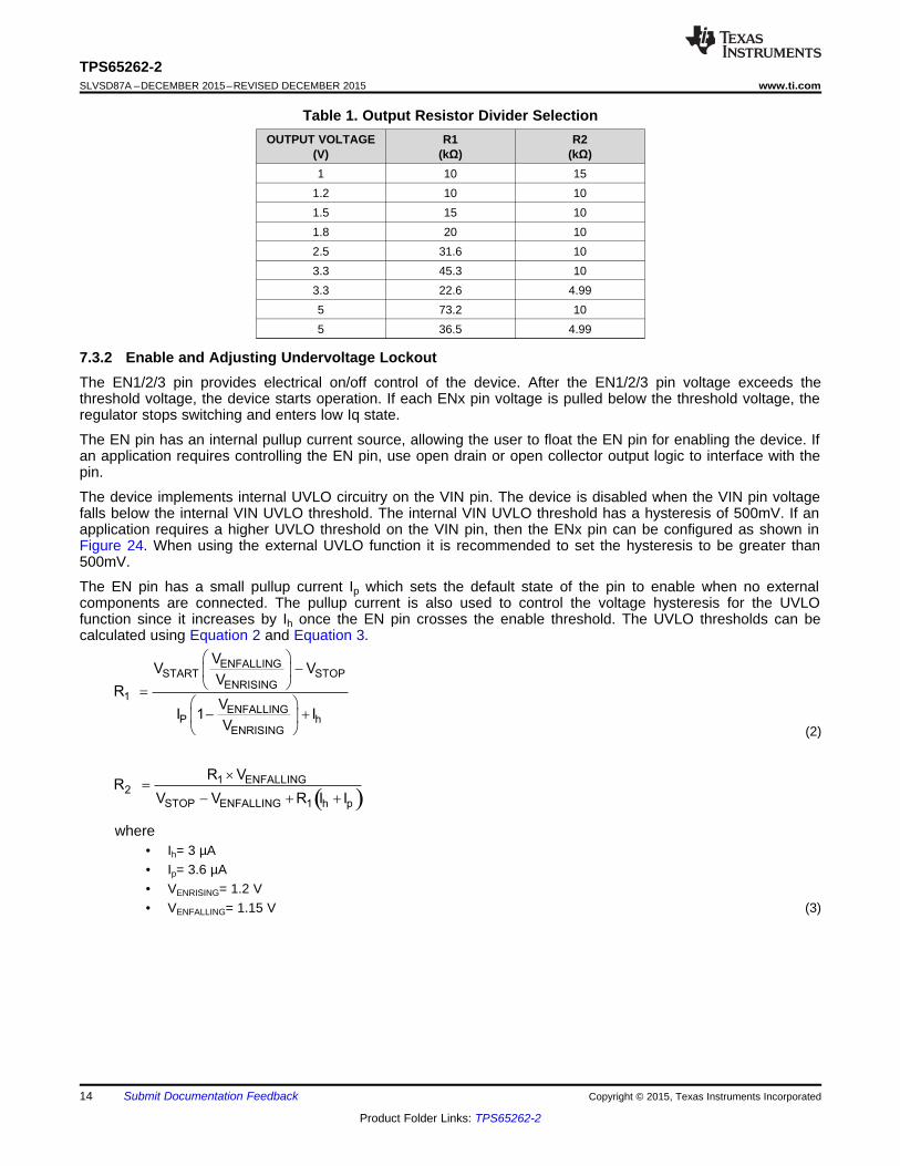
The device implements internal UVLO circuitry on the VIN pin. The device is disabled when the VIN pin voltagefalls below the internal VIN UVLO threshold. The internal VIN UVLO threshold has a hysteresis of 500mV. If anapplication requires a higher UVLO threshold on the VIN pin, then the ENx pin can be configured as shown inFigure 24. When using the external UVLO function it is recommended to set the hysteresis to be greater than500mV.
The EN pin has a small pullup current Ip which sets the default state of the pin to enable when no externalcomponents are connected. The pullup current is also used to control the voltage hysteresis for the UVLOfunction since it increases by Ih once the EN pin crosses the enable threshold. The UVLO thresholds can becalculated using Equation 2 and Equation 3.
(2)
spacer
where• Ih= 3 µA• Ip= 3.6 µA• VENRISING= 1.2 V• VENFALLING= 1.15 V (3)
14 Submit Documentation Feedback Copyright © 2015, Texas Instruments Incorporated
Product Folder Links: TPS65262-2
0.6VTss(ms) Css(nF)
5 A
æ ö= ´ ç ÷mè ø
VIN
R1
R2EN
i
ih
p
TPS65262-2www.ti.com SLVSD87A –DECEMBER 2015–REVISED DECEMBER 2015
Figure 24. Adjustable VIN Undervoltage Lockout
7.3.3 Soft-Start TimeThe voltage on the SS1 pin controls the start-up of buck1 output. When the voltage on the SS1 pin is less thanthe internal 0.6-V reference, The TPS65262-2 regulates the internal feedback voltage to the voltage on the SS1pin instead of 0.6 V, allowing VOUT to rise smoothly from 0 V to its regulated voltage without inrush current. Thedevice has an internal pullup current source of 5 µA (typical) that charges an external soft-start capacitor toprovide a linear ramping voltage at SS1 pin.
Buck1’s soft-start time can be calculated approximately by Equation 4.
Buck2 and Buck3 have fixed 1-ms soft start time.
(4)
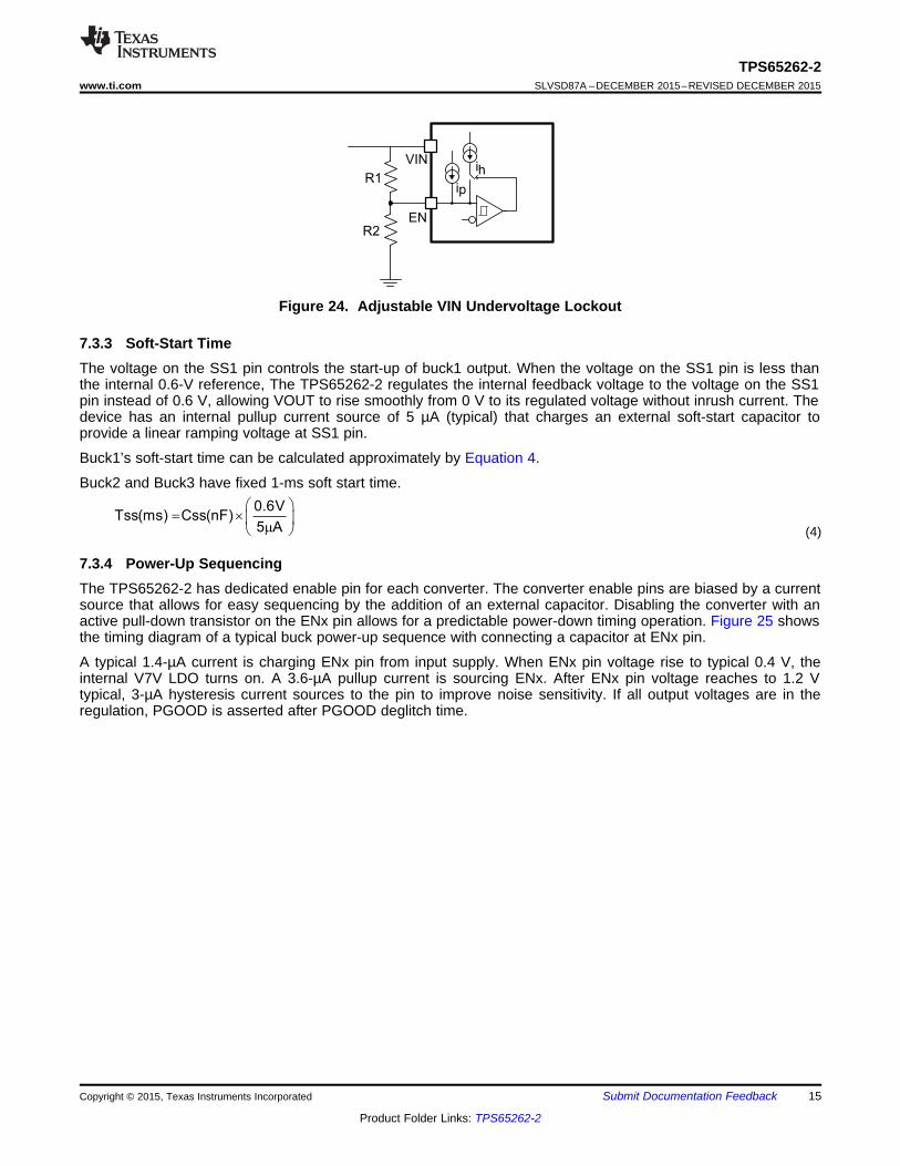
7.3.4 Power-Up SequencingThe TPS65262-2 has dedicated enable pin for each converter. The converter enable pins are biased by a currentsource that allows for easy sequencing by the addition of an external capacitor. Disabling the converter with anactive pull-down transistor on the ENx pin allows for a predictable power-down timing operation. Figure 25 showsthe timing diagram of a typical buck power-up sequence with connecting a capacitor at ENx pin.
A typical 1.4-µA current is charging ENx pin from input supply. When ENx pin voltage rise to typical 0.4 V, theinternal V7V LDO turns on. A 3.6-µA pullup current is sourcing ENx. After ENx pin voltage reaches to 1.2 Vtypical, 3-µA hysteresis current sources to the pin to improve noise sensitivity. If all output voltages are in theregulation, PGOOD is asserted after PGOOD deglitch time.
Copyright © 2015, Texas Instruments Incorporated Submit Documentation Feedback 15
Product Folder Links: TPS65262-2
EN Threshold
ENx
VOUTx
EN Threshold
PGOOD
VIN
PGOOD Deglitch Time
V7V
Charge CEN
with 6.6uA
Enx Rise TimeDectated by CEN
Pre-Bias Startup
Soft Start Rise TimeDictated by CSS
T = C *0.4V/1.4 uAEN
T = C *(1.2-0.4)V/3.6 uAEN
T = C *0.6V/5 uASS
TPS65262-2SLVSD87A –DECEMBER 2015–REVISED DECEMBER 2015 www.ti.com
Figure 25. Startup Power Sequence
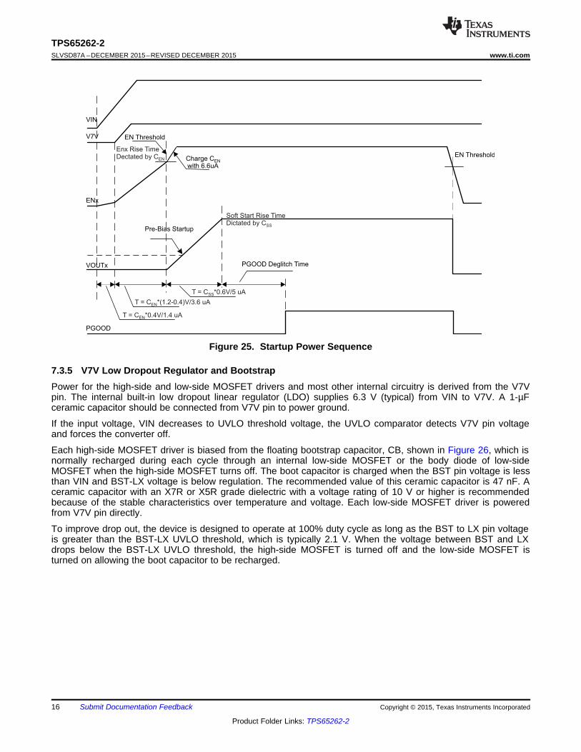
7.3.5 V7V Low Dropout Regulator and BootstrapPower for the high-side and low-side MOSFET drivers and most other internal circuitry is derived from the V7Vpin. The internal built-in low dropout linear regulator (LDO) supplies 6.3 V (typical) from VIN to V7V. A 1-µFceramic capacitor should be connected from V7V pin to power ground.
If the input voltage, VIN decreases to UVLO threshold voltage, the UVLO comparator detects V7V pin voltageand forces the converter off.
Each high-side MOSFET driver is biased from the floating bootstrap capacitor, CB, shown in Figure 26, which isnormally recharged during each cycle through an internal low-side MOSFET or the body diode of low-sideMOSFET when the high-side MOSFET turns off. The boot capacitor is charged when the BST pin voltage is lessthan VIN and BST-LX voltage is below regulation. The recommended value of this ceramic capacitor is 47 nF. Aceramic capacitor with an X7R or X5R grade dielectric with a voltage rating of 10 V or higher is recommendedbecause of the stable characteristics over temperature and voltage. Each low-side MOSFET driver is poweredfrom V7V pin directly.
To improve drop out, the device is designed to operate at 100% duty cycle as long as the BST to LX pin voltageis greater than the BST-LX UVLO threshold, which is typically 2.1 V. When the voltage between BST and LXdrops below the BST-LX UVLO threshold, the high-side MOSFET is turned off and the low-side MOSFET isturned on allowing the boot capacitor to be recharged.
16 Submit Documentation Feedback Copyright © 2015, Texas Instruments Incorporated
Product Folder Links: TPS65262-2
LDO
High-sideMOSFET
Low-sideMOSFET
V7V
VIN PVINx
BSTx
LXx
CB
Cbias1uF
+2.1V
nBootUV
nBootUV
PWM
PWM
nBootUV BootUVProtection
Clk
(V – V )BSTx LXx
UVLOBiasBuck
Controller
GateDriver
GateDriver
TPS65262-2www.ti.com SLVSD87A –DECEMBER 2015–REVISED DECEMBER 2015
Figure 26. V7V Linear Dropout Regulator and Bootstrap Voltage Diagram
7.3.6 Out-of-Phase OperationTo reduce input ripple current, the switch clock of buck1 is 180° out-of-phase from the clock of buck2 and buck3.This enables the system having less input current ripple to reduce input capacitors’ size, cost, and EMI.
7.3.7 Output Overvoltage Protection (OVP)The device incorporates an OVP circuit to minimize output voltage overshoot. When the output is overloaded, theerror amplifier compares the actual output voltage to the internal reference voltage. If the FB pin voltage is lowerthan the internal reference voltage for a considerable time, the output of the error amplifier demands maximumoutput current. Once the condition is removed, the regulator output rises and the error amplifier output transitionsto the steady state voltage. In some applications with small output capacitance, the load can respond faster thanthe error amplifier. This leads to the possibility of an output overshoot. Each buck compares the FB pin voltage tothe OVP threshold. If the FB pin voltage is greater than the OVP threshold, the high-side MOSFET is turned offpreventing current from flowing to the output and minimizing output overshoot. When the FB voltage drops lowerthan the OVP threshold, the high-side MOSFET turns on at the next clock cycle.
7.3.8 PSMIf the MODE pin is connected to GND, the TPS65262-2 can enter high-efficiency PSM operation at light loadcurrent.
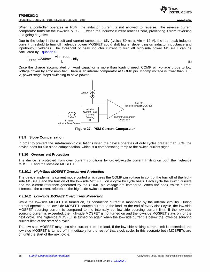
When a controller is enabled for PSM operation, the peak inductor current is sensed and compared with 230-mAcurrent typically. Since the integrated current comparator catches the peak inductor current only, the averageload current entering PSM varies with the applications and external output filters. In PSM, the sensed peakinductor current is clamped at 230 mA.
Copyright © 2015, Texas Instruments Incorporated Submit Documentation Feedback 17
Product Folder Links: TPS65262-2
IL_Peak
Inductor Peak Current
Inductor
Current Peak
Current
Sensingx1
Current Comparator
Delay: tdly
Turn off
high-side Power MOSFET
230mA
PEAK
vin voutIL 230mA tdly
L
-= + ´
TPS65262-2SLVSD87A –DECEMBER 2015–REVISED DECEMBER 2015 www.ti.com
When a controller operates in PSM, the inductor current is not allowed to reverse. The reverse currentcomparator turns off the low-side MOSFET when the inductor current reaches zero, preventing it from reversingand going negative.
Due to the delay in the circuit and current comparator tdly (typical 50 ns at Vin = 12 V), the real peak inductorcurrent threshold to turn off high-side power MOSFET could shift higher depending on inductor inductance andinput/output voltages. The threshold of peak inductor current to turn off high-side power MOSFET can becalculated by Equation 5.
(5)
Once the charge accumulated on Vout capacitor is more than loading need, COMP pin voltage drops to lowvoltage driven by error amplifier. There is an internal comparator at COMP pin. If comp voltage is lower than 0.35V, power stage stops switching to save power.
Figure 27. PSM Current Comparator
7.3.9 Slope CompensationIn order to prevent the sub-harmonic oscillations when the device operates at duty cycles greater than 50%, thedevice adds built-in slope compensation, which is a compensating ramp to the switch current signal.
7.3.10 Overcurrent ProtectionThe device is protected from over current conditions by cycle-by-cycle current limiting on both the high-sideMOSFET and the low-side MOSFET.
7.3.10.1 High-Side MOSFET Overcurrent ProtectionThe device implements current mode control which uses the COMP pin voltage to control the turn off of the high-side MOSFET and the turn on of the low-side MOSFET on a cycle by cycle basis. Each cycle the switch currentand the current reference generated by the COMP pin voltage are compared. When the peak switch currentintersects the current reference, the high-side switch is turned off.
7.3.10.2 Low-Side MOSFET Overcurrent ProtectionWhile the low-side MOSFET is turned on, its conduction current is monitored by the internal circuitry. Duringnormal operation the low-side MOSFET sources current to the load. At the end of every clock cycle, the low-sideMOSFET sourcing current is compared to the internally set low-side sourcing current limit. If the low-sidesourcing current is exceeded, the high-side MOSFET is not turned on and the low-side MOSFET stays on for thenext cycle. The high-side MOSFET is turned on again when the low-side current is below the low-side sourcingcurrent limit at the start of a cycle.
The low-side MOSFET may also sink current from the load. If the low-side sinking current limit is exceeded, thelow-side MOSFET is turned off immediately for the rest of that clock cycle. In this scenario both MOSFETs areoff until the start of the next cycle.
18 Submit Documentation Feedback Copyright © 2015, Texas Instruments Incorporated
Product Folder Links: TPS65262-2
OC limiting (waiting) time
0.5mshiccup time
14ms
soft start time
buck1: T=Css*0.6V/5uA
buck2/3: 1ms
iL
Inductor Current
SS
SS Pin Voltage
Vout
Output Voltage
Soft-start is reset after OC waiting time
OC fault removed, soft-start & output recovery 0.6V
~2.1V
Output over loading
OCP peak inductor current threshold
Output hard short circuit
TPS65262-2www.ti.com SLVSD87A –DECEMBER 2015–REVISED DECEMBER 2015
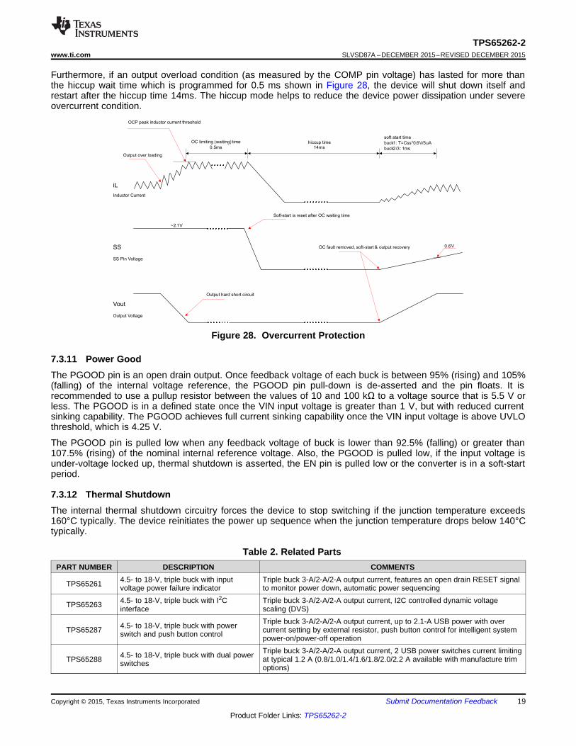
Furthermore, if an output overload condition (as measured by the COMP pin voltage) has lasted for more thanthe hiccup wait time which is programmed for 0.5 ms shown in Figure 28, the device will shut down itself andrestart after the hiccup time 14ms. The hiccup mode helps to reduce the device power dissipation under severeovercurrent condition.
Figure 28. Overcurrent Protection
7.3.11 Power GoodThe PGOOD pin is an open drain output. Once feedback voltage of each buck is between 95% (rising) and 105%(falling) of the internal voltage reference, the PGOOD pin pull-down is de-asserted and the pin floats. It isrecommended to use a pullup resistor between the values of 10 and 100 kΩ to a voltage source that is 5.5 V orless. The PGOOD is in a defined state once the VIN input voltage is greater than 1 V, but with reduced currentsinking capability. The PGOOD achieves full current sinking capability once the VIN input voltage is above UVLOthreshold, which is 4.25 V.
The PGOOD pin is pulled low when any feedback voltage of buck is lower than 92.5% (falling) or greater than107.5% (rising) of the nominal internal reference voltage. Also, the PGOOD is pulled low, if the input voltage isunder-voltage locked up, thermal shutdown is asserted, the EN pin is pulled low or the converter is in a soft-startperiod.
7.3.12 Thermal ShutdownThe internal thermal shutdown circuitry forces the device to stop switching if the junction temperature exceeds160°C typically. The device reinitiates the power up sequence when the junction temperature drops below 140°Ctypically.
Table 2. Related PartsPART NUMBER DESCRIPTION COMMENTS
4.5- to 18-V, triple buck with input Triple buck 3-A/2-A/2-A output current, features an open drain RESET signalTPS65261 voltage power failure indicator to monitor power down, automatic power sequencing4.5- to 18-V, triple buck with I2C Triple buck 3-A/2-A/2-A output current, I2C controlled dynamic voltageTPS65263 interface scaling (DVS)
Triple buck 3-A/2-A/2-A output current, up to 2.1-A USB power with over4.5- to 18-V, triple buck with powerTPS65287 current setting by external resistor, push button control for intelligent systemswitch and push button control power-on/power-off operationTriple buck 3-A/2-A/2-A output current, 2 USB power switches current limiting4.5- to 18-V, triple buck with dual powerTPS65288 at typical 1.2 A (0.8/1.0/1.4/1.6/1.8/2.0/2.2 A available with manufacture trimswitches options)
Copyright © 2015, Texas Instruments Incorporated Submit Documentation Feedback 19
Product Folder Links: TPS65262-2
TPS65262-2SLVSD87A –DECEMBER 2015–REVISED DECEMBER 2015 www.ti.com
7.4 Device Functional Modes
7.4.1 Operation With VIN < 4.5 V (Minimum VIN)The device operates with input voltages above 4.5 V. The maximum UVLO voltage is 4.5 V and operates at inputvoltages above 4.5 V. The typical UVLO voltage is 4.25 V, and the device may operate at input voltages abovethat point. The device also may operate at lower input voltages; the minimum UVLO voltage is 4 V (rising) and3.5 V (falling). At input voltages below the UVLO minimum voltage, the device does not operate.
7.4.2 Operation With EN ControlThe enable rising edge threshold voltage is 1.2 V typical and 1.26 V maximum. With EN held below that voltage,the device is disabled and switching is inhibited. The IC quiescent current is reduced in this state. When the inputvoltage is above the UVLO threshold and the EN voltage is increased above the rising edge threshold, thedevice becomes active. Switching is enabled, and the soft-start sequence is initiated. The device starts at thesoft-start time determined by the external soft start capacitor as shown in Figure 31 to Figure 36.
20 Submit Documentation Feedback Copyright © 2015, Texas Instruments Incorporated
Product Folder Links: TPS65262-2
BST1
VIN1
LX1
LE
N2
EN
1
FB
1
PGND1
LV
IN2
SS
1
LOUT1
LVIN1
Vout1
+1.2V
Max. 3A
Vin
CO
MP
1
LO
UT
2
LF
B2
LEN1
LFB1
4.7uH
10uF
47nF
3.3nF
20K
20K
10K
31.6K
20K
1 2 43
24
23
21
22
25
26
27
28
29
30
31
32
L1
C13
R42
R40
C4
C5R1
22uFC10 C11
22uF
R4
0
82pFC1
R11
R12
22pF
C8
BST2
LX2
VIN2
PGND2
PGND3
VIN3
LX3
MO
DE
BST3F
B3
PG
OO
D
EN
3
Vin
V7
V
AG
ND
Vout3
+3.3V
Max. 1A
Vout2
+1.8V
Max. 1A
FB
2
EN
2
Vin
4.7uH
4.7uH
47nF
47nF
10uF
10uF
1uF
45.3K
20K
10K
10K
5 6 87
20
19
17
18
16
15
14
13
12
11
10
9
C17
L2
L3
C15
C14
C6
22uF
22uF
C18
C12
R21
R22C282pF
R6
0
R5
0
R31
R32 22pFC3
C9
TPS65262-2
PG
OO
D100K
R8
Vin_LDO1
Vin_LDO2
LDO1
2.5V
200mA
LDO2
5.0V
100mA4.7uF
C20
1uFC21
73.2KR51
10KR52
4.7uFC19
1uFC16
10nFC7
PU
LL
TPS65262-2www.ti.com SLVSD87A –DECEMBER 2015–REVISED DECEMBER 2015
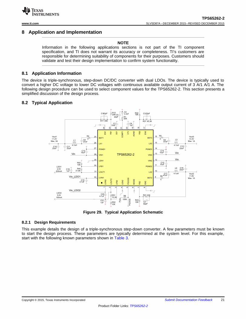
8 Application and Implementation
NOTEInformation in the following applications sections is not part of the TI componentspecification, and TI does not warrant its accuracy or completeness. TI’s customers areresponsible for determining suitability of components for their purposes. Customers shouldvalidate and test their design implementation to confirm system functionality.
8.1 Application InformationThe device is triple-synchronous, step-down DC/DC converter with dual LDOs. The device is typically used toconvert a higher DC voltage to lower DC voltages with continuous available output current of 3 A/1 A/1 A. Thefollowing design procedure can be used to select component values for the TPS65262-2. This section presents asimplified discussion of the design process.
8.2 Typical Application
Figure 29. Typical Application Schematic
8.2.1 Design RequirementsThis example details the design of a triple-synchronous step-down converter. A few parameters must be knownto start the design process. These parameters are typically determined at the system level. For this example,start with the following known parameters shown in Table 3.
Copyright © 2015, Texas Instruments Incorporated Submit Documentation Feedback 21
Product Folder Links: TPS65262-2
rippleLpeak out
II I
2= +
( ) 2
out inmax out
inmax sw2Lrms O
V V V
V L ƒI I
12
æ ö´ -ç ÷ç ÷´ ´è ø= +
inmax out outripple
inmax sw
V V VI
L V ƒ
-
= ´
´
inmax out out
o inmax sw
V V VL
I LIR V ƒ
-
= ´
´ ´
TPS65262-2SLVSD87A –DECEMBER 2015–REVISED DECEMBER 2015 www.ti.com
Table 3. Design ParametersPARAMETER VALUE
Vout1 1.2 VIout1 3 AVout2 1.8 VIout2 1 AVout3 3.3 VIout3 1 A
Buck1 transient response 1-A load step ±5%Buck2, buck3 transient response 0.5-A load step ±5%
Input voltage 12 V normal, 4.5 to 18 VOutput voltage ripple ±1%Switching frequency 600 kHz
8.2.2 Detailed Design Procedure
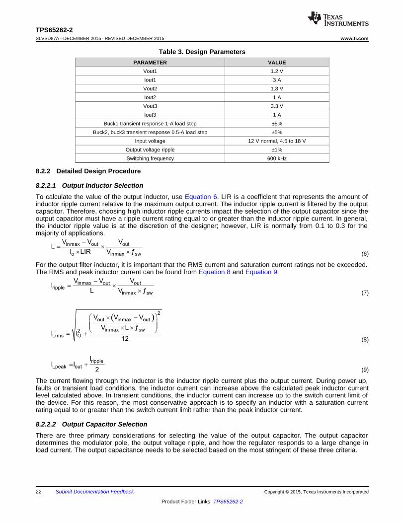
8.2.2.1 Output Inductor SelectionTo calculate the value of the output inductor, use Equation 6. LIR is a coefficient that represents the amount ofinductor ripple current relative to the maximum output current. The inductor ripple current is filtered by the outputcapacitor. Therefore, choosing high inductor ripple currents impact the selection of the output capacitor since theoutput capacitor must have a ripple current rating equal to or greater than the inductor ripple current. In general,the inductor ripple value is at the discretion of the designer; however, LIR is normally from 0.1 to 0.3 for themajority of applications.
(6)
For the output filter inductor, it is important that the RMS current and saturation current ratings not be exceeded.The RMS and peak inductor current can be found from Equation 8 and Equation 9.
(7)
spacer
(8)
spacer
(9)
The current flowing through the inductor is the inductor ripple current plus the output current. During power up,faults or transient load conditions, the inductor current can increase above the calculated peak inductor currentlevel calculated above. In transient conditions, the inductor current can increase up to the switch current limit ofthe device. For this reason, the most conservative approach is to specify an inductor with a saturation currentrating equal to or greater than the switch current limit rather than the peak inductor current.
8.2.2.2 Output Capacitor SelectionThere are three primary considerations for selecting the value of the output capacitor. The output capacitordetermines the modulator pole, the output voltage ripple, and how the regulator responds to a large change inload current. The output capacitance needs to be selected based on the most stringent of these three criteria.
22 Submit Documentation Feedback Copyright © 2015, Texas Instruments Incorporated
Product Folder Links: TPS65262-2
( )inmin outoutinrms out
inmin inmin
V VVI I
V V
-= ´ ´
( )out inmax outcorms
inmax sw
V V VI
12 V L ƒ
´ -=
´ ´ ´
orippleesr
oripple
VR
I<
ooripplesw
oripple
1 1C
V8 ƒ
I
> ´
´
outo
sw out
2 IC
ƒ V
´ D=
´ D
TPS65262-2www.ti.com SLVSD87A –DECEMBER 2015–REVISED DECEMBER 2015
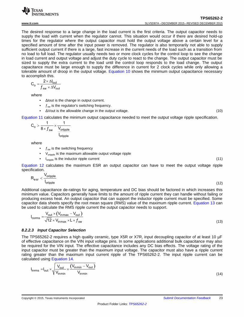
The desired response to a large change in the load current is the first criteria. The output capacitor needs tosupply the load with current when the regulator cannot. This situation would occur if there are desired hold-uptimes for the regulator where the output capacitor must hold the output voltage above a certain level for aspecified amount of time after the input power is removed. The regulator is also temporarily not able to supplysufficient output current if there is a large, fast increase in the current needs of the load such as a transition fromno load to full load. The regulator usually needs two or more clock cycles for the control loop to see the changein load current and output voltage and adjust the duty cycle to react to the change. The output capacitor must besized to supply the extra current to the load until the control loop responds to the load change. The outputcapacitance must be large enough to supply the difference in current for 2 clock cycles while only allowing atolerable amount of droop in the output voltage. Equation 10 shows the minimum output capacitance necessaryto accomplish this.
where• ΔIout is the change in output current.• ƒsw is the regulator's switching frequency.• ΔVout is the allowable change in the output voltage. (10)
Equation 11 calculates the minimum output capacitance needed to meet the output voltage ripple specification.
where• ƒsw is the switching frequency• Voripple is the maximum allowable output voltage ripple• Ioripple is the inductor ripple current (11)
Equation 12 calculates the maximum ESR an output capacitor can have to meet the output voltage ripplespecification.
(12)
Additional capacitance de-ratings for aging, temperature and DC bias should be factored in which increases thisminimum value. Capacitors generally have limits to the amount of ripple current they can handle without failing orproducing excess heat. An output capacitor that can support the inductor ripple current must be specified. Somecapacitor data sheets specify the root mean square (RMS) value of the maximum ripple current. Equation 13 canbe used to calculate the RMS ripple current the output capacitor needs to support.
(13)
8.2.2.3 Input Capacitor SelectionThe TPS65262-2 requires a high quality ceramic, type X5R or X7R, input decoupling capacitor of at least 10 µFof effective capacitance on the VIN input voltage pins. In some applications additional bulk capacitance may alsobe required for the VIN input. The effective capacitance includes any DC bias effects. The voltage rating of theinput capacitor must be greater than the maximum input voltage. The capacitor must also have a ripple currentrating greater than the maximum input current ripple of The TPS65262-2. The input ripple current can becalculated using Equation 14.
(14)
Copyright © 2015, Texas Instruments Incorporated Submit Documentation Feedback 23
Product Folder Links: TPS65262-2
c
1C 1 =
5 ¦S u u
ESRb
C
R CoC
R
´
=
LC
C
R CoC
R
´
=
o L
1ƒp .
C R 2
æ ö=ç ÷
´ ´ pè ø
C
m EA m PS
2 fc Vo CoR
G Vref G- -
p ´ ´ ´
=
´ ´
outmaxin
in sw
I 0.25V
C ƒ
´D =
´
TPS65262-2SLVSD87A –DECEMBER 2015–REVISED DECEMBER 2015 www.ti.com
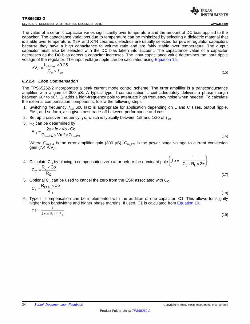
The value of a ceramic capacitor varies significantly over temperature and the amount of DC bias applied to thecapacitor. The capacitance variations due to temperature can be minimized by selecting a dielectric material thatis stable over temperature. X5R and X7R ceramic dielectrics are usually selected for power regulator capacitorsbecause they have a high capacitance to volume ratio and are fairly stable over temperature. The outputcapacitor must also be selected with the DC bias taken into account. The capacitance value of a capacitordecreases as the DC bias across a capacitor increases. The input capacitance value determines the input ripplevoltage of the regulator. The input voltage ripple can be calculated using Equation 15.
(15)
8.2.2.4 Loop CompensationThe TPS65262-2 incorporates a peak current mode control scheme. The error amplifier is a transconductanceamplifier with a gain of 300 µS. A typical type II compensation circuit adequately delivers a phase marginbetween 60° to 90°. Cb adds a high-frequency pole to attenuate high frequency noise when needed. To calculatethe external compensation components, follow the following steps.1. Switching frequency ƒsw 600 kHz is appropriate for application depending on L and C sizes, output ripple,
EMI, and so forth, also gives best trade-off between performance and cost.2. Set up crossover frequency, ƒc, which is typically between 1/5 and 1/20 of ƒsw.3. RC can be determined by
(16)
Where Gm_EA is the error amplifier gain (300 µS), Gm_PS is the power stage voltage to current conversiongain (7.4 A/V).
4. Calculate CC by placing a compensation zero at or before the dominant pole
(17)5. Optional Cb can be used to cancel the zero from the ESR associated with CO.
(18)6. Type III compensation can be implemented with the addition of one capacitor, C1. This allows for slightly
higher loop bandwidths and higher phase margins. If used, C1 is calculated from Equation 19.
(19)
24 Submit Documentation Feedback Copyright © 2015, Texas Instruments Incorporated
Product Folder Links: TPS65262-2
Current SenseI/V Converter
COMPVfb
EA
LX
FB
VOUT
RESR
RL
CO
iL
Gm_PS = 7.4 A/V
C1R1
R2
Vref = 0.6 V
Cb
Cc
Rc Gm_EA = 300 µS
TPS65262-2www.ti.com SLVSD87A –DECEMBER 2015–REVISED DECEMBER 2015
Figure 30. DC/DC Loop Compensation
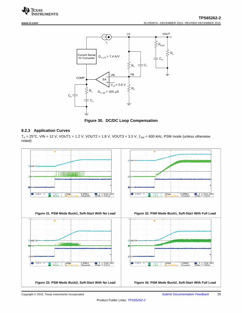
8.2.3 Application CurvesTA = 25°C, VIN = 12 V, VOUT1 = 1.2 V, VOUT2 = 1.8 V, VOUT3 = 3.3 V, ƒSW = 600 kHz, PSM mode (unless otherwisenoted)
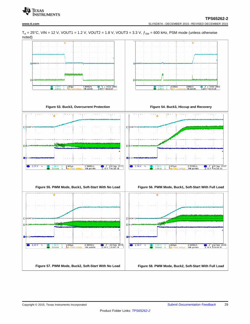
Figure 31. PSM Mode Buck1, Soft-Start With No Load Figure 32. PSM Mode Buck1, Soft-Start With Full Load
Figure 33. PSM Mode Buck2, Soft-Start With No Load Figure 34. PSM Mode Buck2, Soft-Start With Full Load
Copyright © 2015, Texas Instruments Incorporated Submit Documentation Feedback 25
Product Folder Links: TPS65262-2
TPS65262-2SLVSD87A –DECEMBER 2015–REVISED DECEMBER 2015 www.ti.com
TA = 25°C, VIN = 12 V, VOUT1 = 1.2 V, VOUT2 = 1.8 V, VOUT3 = 3.3 V, ƒSW = 600 kHz, PSM mode (unless otherwisenoted)
Figure 35. PSM Mode Buck3, Soft-Start With No Load Figure 36. PSM Mode Buck3, Soft-Start With Full Load
Figure 37. PSM Mode Buck1, Steady State Operation Figure 38. Buck1, Steady State OperationWith Light Load With Full Load
Figure 39. PSM Mode Buck2, Steady State Operation Figure 40. Buck2, Steady State OperationWith Light Load With Full Load
26 Submit Documentation Feedback Copyright © 2015, Texas Instruments Incorporated
Product Folder Links: TPS65262-2
TPS65262-2www.ti.com SLVSD87A –DECEMBER 2015–REVISED DECEMBER 2015
TA = 25°C, VIN = 12 V, VOUT1 = 1.2 V, VOUT2 = 1.8 V, VOUT3 = 3.3 V, ƒSW = 600 kHz, PSM mode (unless otherwisenoted)
Figure 41. PSM Mode Buck3, Steady State Operation Figure 42. Buck3, Steady State OperationWith Light Load With Full Load
Figure 43. Buck1, Load Transient, 0.75 to 1.5 A Figure 44. Buck1, Load Transient, 1.5 to 2.25 ASR = 0.25 A/µs SR = 0.25 A/µs
Figure 45. Buck2, Load Transient, 0.25 to 0.5 A Figure 46. Buck2, Load Transient, 0.5 to 0.75 ASR = 0.25 A/µs SR = 0.25A/µs
Copyright © 2015, Texas Instruments Incorporated Submit Documentation Feedback 27
Product Folder Links: TPS65262-2
TPS65262-2SLVSD87A –DECEMBER 2015–REVISED DECEMBER 2015 www.ti.com
TA = 25°C, VIN = 12 V, VOUT1 = 1.2 V, VOUT2 = 1.8 V, VOUT3 = 3.3 V, ƒSW = 600 kHz, PSM mode (unless otherwisenoted)
Figure 47. Buck3, Load Transient, 0.25 to 0.5 A Figure 48. Buck3, Load Transient, 0.5 to 0.75 ASR = 0.25 A/µs SR = 0.25A/µs
Figure 49. Buck1, Overcurrent Protection Figure 50. Buck1, Hiccup and Recovery
Figure 51. Buck2, Overcurrent Protection Figure 52. Buck2, Hiccup and Recovery
28 Submit Documentation Feedback Copyright © 2015, Texas Instruments Incorporated
Product Folder Links: TPS65262-2
TPS65262-2www.ti.com SLVSD87A –DECEMBER 2015–REVISED DECEMBER 2015
TA = 25°C, VIN = 12 V, VOUT1 = 1.2 V, VOUT2 = 1.8 V, VOUT3 = 3.3 V, ƒSW = 600 kHz, PSM mode (unless otherwisenoted)
Figure 53. Buck3, Overcurrent Protection Figure 54. Buck3, Hiccup and Recovery
Figure 55. PWM Mode, Buck1, Soft-Start With No Load Figure 56. PWM Mode, Buck1, Soft-Start With Full Load
Figure 57. PWM Mode, Buck2, Soft-Start With No Load Figure 58. PWM Mode, Buck2, Soft-Start With Full Load
Copyright © 2015, Texas Instruments Incorporated Submit Documentation Feedback 29
Product Folder Links: TPS65262-2
TPS65262-2SLVSD87A –DECEMBER 2015–REVISED DECEMBER 2015 www.ti.com
TA = 25°C, VIN = 12 V, VOUT1 = 1.2 V, VOUT2 = 1.8 V, VOUT3 = 3.3 V, ƒSW = 600 kHz, PSM mode (unless otherwisenoted)
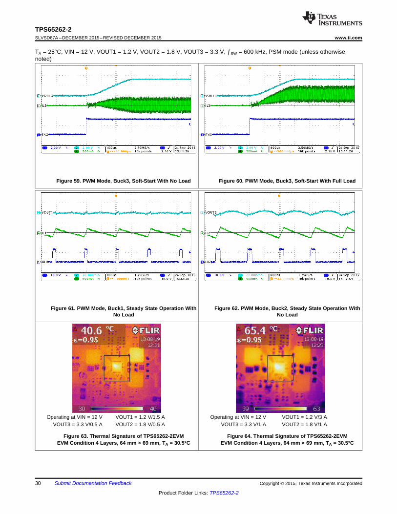
Figure 59. PWM Mode, Buck3, Soft-Start With No Load Figure 60. PWM Mode, Buck3, Soft-Start With Full Load
Figure 61. PWM Mode, Buck1, Steady State Operation With Figure 62. PWM Mode, Buck2, Steady State Operation WithNo Load No Load
Operating at VIN = 12 V VOUT1 = 1.2 V/1.5 A Operating at VIN = 12 V VOUT1 = 1.2 V/3 AVOUT3 = 3.3 V/0.5 A VOUT2 = 1.8 V/0.5 A VOUT3 = 3.3 V/1 A VOUT2 = 1.8 V/1 A
Figure 63. Thermal Signature of TPS65262-2EVM Figure 64. Thermal Signature of TPS65262-2EVMEVM Condition 4 Layers, 64 mm × 69 mm, TA = 30.5°C EVM Condition 4 Layers, 64 mm × 69 mm, TA = 30.5°C
30 Submit Documentation Feedback Copyright © 2015, Texas Instruments Incorporated
Product Folder Links: TPS65262-2
TPS65262-2www.ti.com SLVSD87A –DECEMBER 2015–REVISED DECEMBER 2015
9 Power Supply Recommendations
A wide 4.5- to 18-V input supply voltage range encompasses the most intermediate bus voltage operating off 5-,9-, 12-, or 15-V power bus. The converter, with constant frequency peak current mode, is designed to simplify itsapplication while giving designers options to optimize the system according to targeted applications.
10 Layout
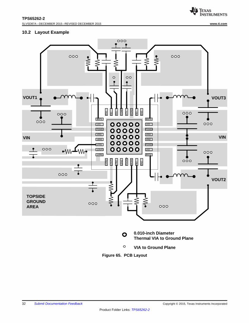
10.1 Layout GuidelinesThe TPS65262-2 supports a 2-layer PCB layout, shown in Figure 65.
Layout is a critical portion of good power supply design. See Figure 65 for a PCB layout example. The topcontains the main power traces for VIN, VOUT, and LX. Also on the top layer are connections for the remainingpins of the TPS65262-2 and a large top side area filled with ground. The top layer ground area should beconnected to the bottom layer ground using vias at the input bypass capacitor, the output filter capacitor anddirectly under the TPS65262-2 device to provide a thermal path from the exposed thermal pad land to ground.The bottom layer acts as ground plane connecting analog ground and power ground.
For operation at full rated load, the top side ground area together with the bottom side ground plane must provideadequate heat dissipating area. There are several signals paths that conduct fast changing currents or voltagesthat can interact with stray inductance or parasitic capacitance to generate noise or degrade the power suppliesperformance. To help eliminate these problems, the VIN pin should be bypassed to ground with a low ESRceramic bypass capacitor with X5R or X7R dielectric. Care should be taken to minimize the loop area formed bythe bypass capacitor connections, the VIN pins, and the ground connections. The VIN pin must also be bypassedto ground using a low-ESR ceramic capacitor with X5R or X7R dielectric.
Since the LX connection is the switching node, the output inductor should be located close to the LX pins, andthe area of the PCB conductor minimized to prevent excessive capacitive coupling. The output filter capacitorground should use the same power ground trace as the VIN input bypass capacitor. Try to minimize thisconductor length while maintaining adequate width. The small signal components should be grounded to theanalog ground path.
The FB and COMP pins are sensitive to noise so the resistors and capacitors should be located as close aspossible to the IC and routed with minimal lengths of trace. The additional external components can be placedapproximately as shown.
Copyright © 2015, Texas Instruments Incorporated Submit Documentation Feedback 31
Product Folder Links: TPS65262-2
LOU
T2
LFB
2
LVIN
2
LEN
2
MO
DE
FB
2
EN
2
PG
OO
D
FB
1
SS
1
EN
1
CO
MP
1
AG
ND
FB
3
EN
3
V7V
LX1
PGND1
BST1
VIN1
LFB1
LOUT1
LVIN1
LEN1
LX3
PGND3
BST3
VIN3
PGND2
LX2
BST2
VIN2VIN
VOUT2
VOUT3VOUT1
VIN
TOPSIDEGROUNDAREA
0.010-inch DiameterThermal VIA to Ground Plane
VIA to Ground Plane
TPS65262-2SLVSD87A –DECEMBER 2015–REVISED DECEMBER 2015 www.ti.com
10.2 Layout Example
Figure 65. PCB Layout
32 Submit Documentation Feedback Copyright © 2015, Texas Instruments Incorporated
Product Folder Links: TPS65262-2
TPS65262-2www.ti.com SLVSD87A –DECEMBER 2015–REVISED DECEMBER 2015
11 Device and Documentation Support
11.1 Community ResourcesThe following links connect to TI community resources. Linked contents are provided "AS IS" by the respectivecontributors. They do not constitute TI specifications and do not necessarily reflect TI's views; see TI's Terms ofUse.
TI E2E™ Online Community TI's Engineer-to-Engineer (E2E) Community. Created to foster collaborationamong engineers. At e2e.ti.com, you can ask questions, share knowledge, explore ideas and helpsolve problems with fellow engineers.
Design Support TI's Design Support Quickly find helpful E2E forums along with design support tools andcontact information for technical support.
11.2 TrademarksE2E is a trademark of Texas Instruments.All other trademarks are the property of their respective owners.
11.3 Electrostatic Discharge CautionThese devices have limited built-in ESD protection. The leads should be shorted together or the device placed in conductive foamduring storage or handling to prevent electrostatic damage to the MOS gates.
11.4 GlossarySLYZ022 — TI Glossary.
This glossary lists and explains terms, acronyms, and definitions.
12 Mechanical, Packaging, and Orderable InformationThe following pages include mechanical, packaging, and orderable information. This information is the mostcurrent data available for the designated devices. This data is subject to change without notice and revision ofthis document. For browser-based versions of this data sheet, refer to the left-hand navigation.
Copyright © 2015, Texas Instruments Incorporated Submit Documentation Feedback 33
Product Folder Links: TPS65262-2
PACKAGE OPTION ADDENDUM
www.ti.com 18-Dec-2015
Addendum-Page 1
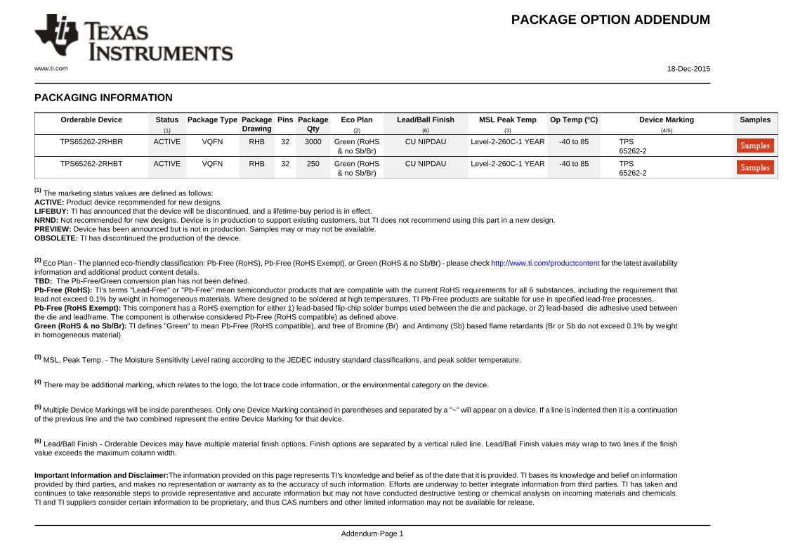
PACKAGING INFORMATION
Orderable Device Status(1)
Package Type PackageDrawing
Pins PackageQty
Eco Plan(2)
Lead/Ball Finish(6)
MSL Peak Temp(3)
Op Temp (°C) Device Marking(4/5)
Samples
TPS65262-2RHBR ACTIVE VQFN RHB 32 3000 Green (RoHS& no Sb/Br)
CU NIPDAU Level-2-260C-1 YEAR -40 to 85 TPS65262-2
TPS65262-2RHBT ACTIVE VQFN RHB 32 250 Green (RoHS& no Sb/Br)
CU NIPDAU Level-2-260C-1 YEAR -40 to 85 TPS65262-2
(1) The marketing status values are defined as follows:ACTIVE: Product device recommended for new designs.LIFEBUY: TI has announced that the device will be discontinued, and a lifetime-buy period is in effect.NRND: Not recommended for new designs. Device is in production to support existing customers, but TI does not recommend using this part in a new design.PREVIEW: Device has been announced but is not in production. Samples may or may not be available.OBSOLETE: TI has discontinued the production of the device.
(2) Eco Plan - The planned eco-friendly classification: Pb-Free (RoHS), Pb-Free (RoHS Exempt), or Green (RoHS & no Sb/Br) - please check http://www.ti.com/productcontent for the latest availabilityinformation and additional product content details.TBD: The Pb-Free/Green conversion plan has not been defined.Pb-Free (RoHS): TI's terms "Lead-Free" or "Pb-Free" mean semiconductor products that are compatible with the current RoHS requirements for all 6 substances, including the requirement thatlead not exceed 0.1% by weight in homogeneous materials. Where designed to be soldered at high temperatures, TI Pb-Free products are suitable for use in specified lead-free processes.Pb-Free (RoHS Exempt): This component has a RoHS exemption for either 1) lead-based flip-chip solder bumps used between the die and package, or 2) lead-based die adhesive used betweenthe die and leadframe. The component is otherwise considered Pb-Free (RoHS compatible) as defined above.Green (RoHS & no Sb/Br): TI defines "Green" to mean Pb-Free (RoHS compatible), and free of Bromine (Br) and Antimony (Sb) based flame retardants (Br or Sb do not exceed 0.1% by weightin homogeneous material)
(3) MSL, Peak Temp. - The Moisture Sensitivity Level rating according to the JEDEC industry standard classifications, and peak solder temperature.
(4) There may be additional marking, which relates to the logo, the lot trace code information, or the environmental category on the device.
(5) Multiple Device Markings will be inside parentheses. Only one Device Marking contained in parentheses and separated by a "~" will appear on a device. If a line is indented then it is a continuationof the previous line and the two combined represent the entire Device Marking for that device.
(6) Lead/Ball Finish - Orderable Devices may have multiple material finish options. Finish options are separated by a vertical ruled line. Lead/Ball Finish values may wrap to two lines if the finishvalue exceeds the maximum column width.
Important Information and Disclaimer:The information provided on this page represents TI's knowledge and belief as of the date that it is provided. TI bases its knowledge and belief on informationprovided by third parties, and makes no representation or warranty as to the accuracy of such information. Efforts are underway to better integrate information from third parties. TI has taken andcontinues to take reasonable steps to provide representative and accurate information but may not have conducted destructive testing or chemical analysis on incoming materials and chemicals.TI and TI suppliers consider certain information to be proprietary, and thus CAS numbers and other limited information may not be available for release.
PACKAGE OPTION ADDENDUM
www.ti.com 18-Dec-2015
Addendum-Page 2
In no event shall TI's liability arising out of such information exceed the total purchase price of the TI part(s) at issue in this document sold by TI to Customer on an annual basis.
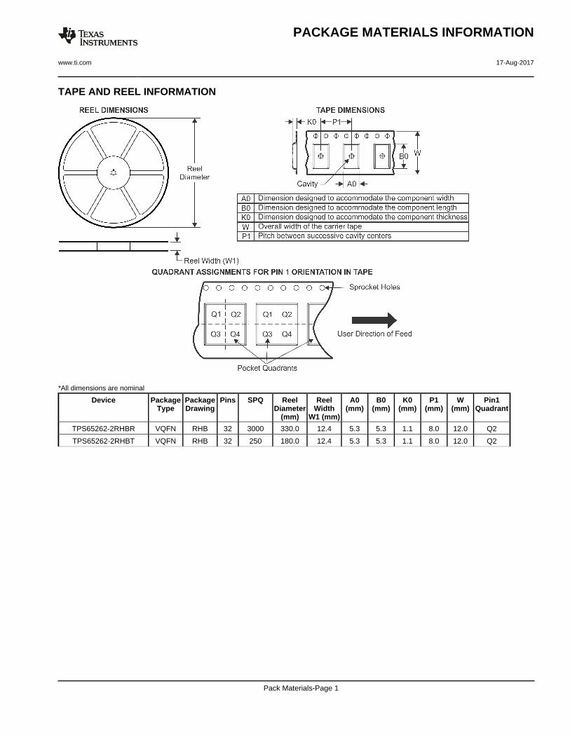
TAPE AND REEL INFORMATION
*All dimensions are nominal
Device PackageType
PackageDrawing
Pins SPQ ReelDiameter
(mm)
ReelWidth
W1 (mm)
A0(mm)
B0(mm)
K0(mm)
P1(mm)
W(mm)
Pin1Quadrant
TPS65262-2RHBR VQFN RHB 32 3000 330.0 12.4 5.3 5.3 1.1 8.0 12.0 Q2
TPS65262-2RHBT VQFN RHB 32 250 180.0 12.4 5.3 5.3 1.1 8.0 12.0 Q2
PACKAGE MATERIALS INFORMATION
www.ti.com 17-Aug-2017
Pack Materials-Page 1
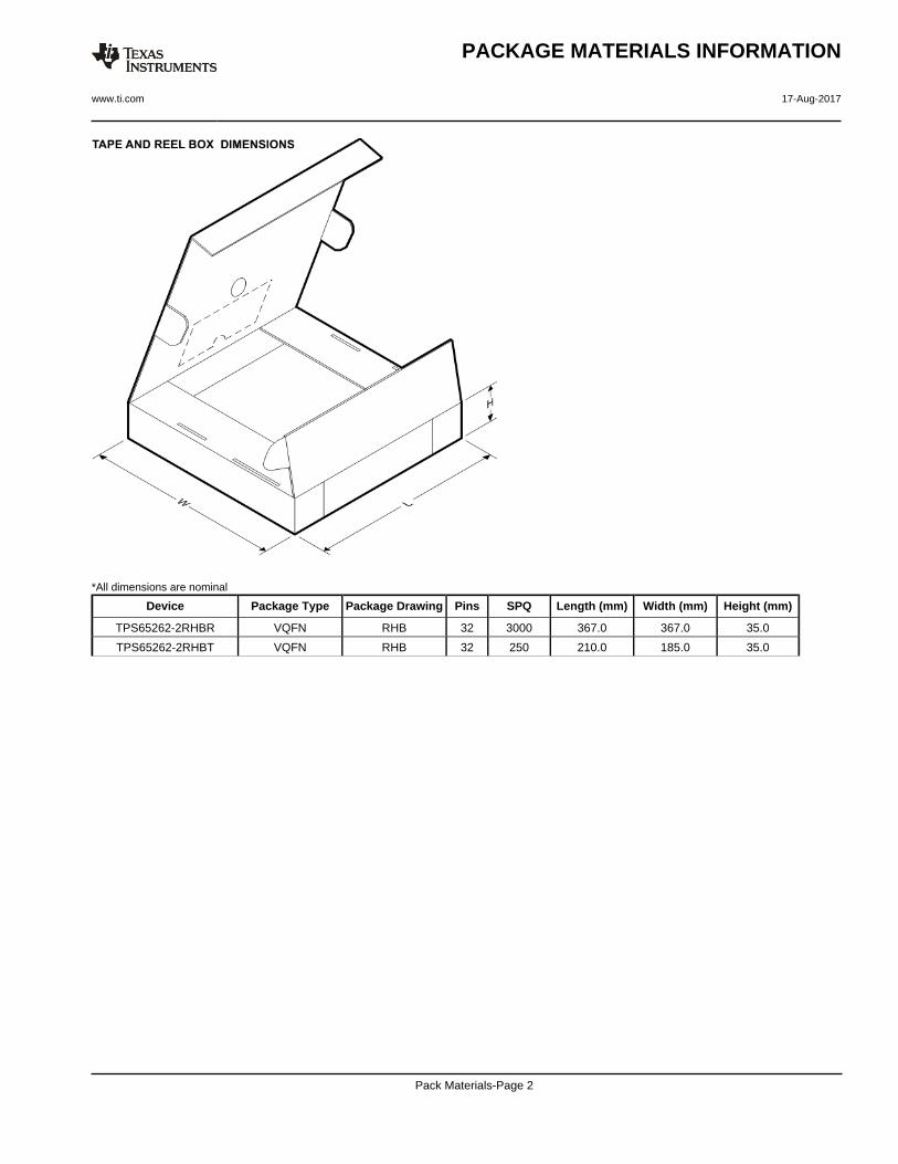
*All dimensions are nominal
Device Package Type Package Drawing Pins SPQ Length (mm) Width (mm) Height (mm)
TPS65262-2RHBR VQFN RHB 32 3000 367.0 367.0 35.0
TPS65262-2RHBT VQFN RHB 32 250 210.0 185.0 35.0
PACKAGE MATERIALS INFORMATION
www.ti.com 17-Aug-2017
Pack Materials-Page 2
IMPORTANT NOTICE
Texas Instruments Incorporated (TI) reserves the right to make corrections, enhancements, improvements and other changes to itssemiconductor products and services per JESD46, latest issue, and to discontinue any product or service per JESD48, latest issue. Buyersshould obtain the latest relevant information before placing orders and should verify that such information is current and complete.TI’s published terms of sale for semiconductor products (http://www.ti.com/sc/docs/stdterms.htm) apply to the sale of packaged integratedcircuit products that TI has qualified and released to market. Additional terms may apply to the use or sale of other types of TI products andservices.Reproduction of significant portions of TI information in TI data sheets is permissible only if reproduction is without alteration and isaccompanied by all associated warranties, conditions, limitations, and notices. TI is not responsible or liable for such reproduceddocumentation. Information of third parties may be subject to additional restrictions. Resale of TI products or services with statementsdifferent from or beyond the parameters stated by TI for that product or service voids all express and any implied warranties for theassociated TI product or service and is an unfair and deceptive business practice. TI is not responsible or liable for any such statements.Buyers and others who are developing systems that incorporate TI products (collectively, “Designers”) understand and agree that Designersremain responsible for using their independent analysis, evaluation and judgment in designing their applications and that Designers havefull and exclusive responsibility to assure the safety of Designers' applications and compliance of their applications (and of all TI productsused in or for Designers’ applications) with all applicable regulations, laws and other applicable requirements. Designer represents that, withrespect to their applications, Designer has all the necessary expertise to create and implement safeguards that (1) anticipate dangerousconsequences of failures, (2) monitor failures and their consequences, and (3) lessen the likelihood of failures that might cause harm andtake appropriate actions. Designer agrees that prior to using or distributing any applications that include TI products, Designer willthoroughly test such applications and the functionality of such TI products as used in such applications.TI’s provision of technical, application or other design advice, quality characterization, reliability data or other services or information,including, but not limited to, reference designs and materials relating to evaluation modules, (collectively, “TI Resources”) are intended toassist designers who are developing applications that incorporate TI products; by downloading, accessing or using TI Resources in anyway, Designer (individually or, if Designer is acting on behalf of a company, Designer’s company) agrees to use any particular TI Resourcesolely for this purpose and subject to the terms of this Notice.TI’s provision of TI Resources does not expand or otherwise alter TI’s applicable published warranties or warranty disclaimers for TIproducts, and no additional obligations or liabilities arise from TI providing such TI Resources. TI reserves the right to make corrections,enhancements, improvements and other changes to its TI Resources. TI has not conducted any testing other than that specificallydescribed in the published documentation for a particular TI Resource.Designer is authorized to use, copy and modify any individual TI Resource only in connection with the development of applications thatinclude the TI product(s) identified in such TI Resource. NO OTHER LICENSE, EXPRESS OR IMPLIED, BY ESTOPPEL OR OTHERWISETO ANY OTHER TI INTELLECTUAL PROPERTY RIGHT, AND NO LICENSE TO ANY TECHNOLOGY OR INTELLECTUAL PROPERTYRIGHT OF TI OR ANY THIRD PARTY IS GRANTED HEREIN, including but not limited to any patent right, copyright, mask work right, orother intellectual property right relating to any combination, machine, or process in which TI products or services are used. Informationregarding or referencing third-party products or services does not constitute a license to use such products or services, or a warranty orendorsement thereof. Use of TI Resources may require a license from a third party under the patents or other intellectual property of thethird party, or a license from TI under the patents or other intellectual property of TI.TI RESOURCES ARE PROVIDED “AS IS” AND WITH ALL FAULTS. TI DISCLAIMS ALL OTHER WARRANTIES ORREPRESENTATIONS, EXPRESS OR IMPLIED, REGARDING RESOURCES OR USE THEREOF, INCLUDING BUT NOT LIMITED TOACCURACY OR COMPLETENESS, TITLE, ANY EPIDEMIC FAILURE WARRANTY AND ANY IMPLIED WARRANTIES OFMERCHANTABILITY, FITNESS FOR A PARTICULAR PURPOSE, AND NON-INFRINGEMENT OF ANY THIRD PARTY INTELLECTUALPROPERTY RIGHTS. TI SHALL NOT BE LIABLE FOR AND SHALL NOT DEFEND OR INDEMNIFY DESIGNER AGAINST ANY CLAIM,INCLUDING BUT NOT LIMITED TO ANY INFRINGEMENT CLAIM THAT RELATES TO OR IS BASED ON ANY COMBINATION OFPRODUCTS EVEN IF DESCRIBED IN TI RESOURCES OR OTHERWISE. IN NO EVENT SHALL TI BE LIABLE FOR ANY ACTUAL,DIRECT, SPECIAL, COLLATERAL, INDIRECT, PUNITIVE, INCIDENTAL, CONSEQUENTIAL OR EXEMPLARY DAMAGES INCONNECTION WITH OR ARISING OUT OF TI RESOURCES OR USE THEREOF, AND REGARDLESS OF WHETHER TI HAS BEENADVISED OF THE POSSIBILITY OF SUCH DAMAGES.Unless TI has explicitly designated an individual product as meeting the requirements of a particular industry standard (e.g., ISO/TS 16949and ISO 26262), TI is not responsible for any failure to meet such industry standard requirements.Where TI specifically promotes products as facilitating functional safety or as compliant with industry functional safety standards, suchproducts are intended to help enable customers to design and create their own applications that meet applicable functional safety standardsand requirements. Using products in an application does not by itself establish any safety features in the application. Designers mustensure compliance with safety-related requirements and standards applicable to their applications. Designer may not use any TI products inlife-critical medical equipment unless authorized officers of the parties have executed a special contract specifically governing such use.Life-critical medical equipment is medical equipment where failure of such equipment would cause serious bodily injury or death (e.g., lifesupport, pacemakers, defibrillators, heart pumps, neurostimulators, and implantables). Such equipment includes, without limitation, allmedical devices identified by the U.S. Food and Drug Administration as Class III devices and equivalent classifications outside the U.S.TI may expressly designate certain products as completing a particular qualification (e.g., Q100, Military Grade, or Enhanced Product).Designers agree that it has the necessary expertise to select the product with the appropriate qualification designation for their applicationsand that proper product selection is at Designers’ own risk. Designers are solely responsible for compliance with all legal and regulatoryrequirements in connection with such selection.Designer will fully indemnify TI and its representatives against any damages, costs, losses, and/or liabilities arising out of Designer’s non-compliance with the terms and provisions of this Notice.
Mailing Address: Texas Instruments, Post Office Box 655303, Dallas, Texas 75265Copyright © 2017, Texas Instruments Incorporated