Embed Size (px)
Citation preview

SUPPLY
GND
TEMP
REF
IOUT1
FAULT
IOUT2
IOUT3
TPS92638-Q1V(bat)
REFHI
IOUT4
IOUT5
IOUT6
IOUT7
IOUT8
Tail
Stop
STOP
PWM4
Stop
PWM3
PWM2
PWM1
EN
Product
Folder
Order
Now
Technical
Documents
Tools &
Software
Support &Community
ReferenceDesign
An IMPORTANT NOTICE at the end of this data sheet addresses availability, warranty, changes, use in safety-critical applications,intellectual property matters and other important disclaimers. PRODUCTION DATA.
TPS92638-Q1SLVSCK5B –SEPTEMBER 2014–REVISED MARCH 2015
TPS92638-Q1 8-Channel Linear LED Driver With PWM Dimming
1
1 Features1• Qualified for Automotive Applications
– Device Temperature Grade 1: –40°C to 125°CAmbient Operating Temperature Range
– Device HBM ESD Classification Level H2– Device CDM ESD Classification Level C3B
• 8-Channel LED Driver With Analog and PWMDimming
• Wide Input-Voltage Range: 5 V–40 V• Adjustable Constant Output Current Set by
Reference Resistor– Maximum Current: 70 mA per Channel– Maximum Current: 560 mA in Parallel
Operation Mode– Accuracy: ±3% per Channel– Accuracy: ±4% per Device
• PWM Dimming Input (PWM)– Turn ON/OFF Delay Time: 25 µs (typ.), 45 µs
(max.)• 4-Bank PWM Dimming to Control 8 Channels• Open- and Shorted-LED Detection With Deglitch• Fault Pin for Open, Short, and Thermal-Shutdown
Failure Reporting, Allowing Parallel BusConnection of up to 15 Devices
• Temperature-Current Foldback to PreventThermal Shutdown, With ProgrammableThreshold
• Single Resistor for Stop-Current Set Point• Single Resistor for Tail-Current Set Point• Operating Junction Temperature Range –40°C to
150°C• Package: 20-Pin Thermally Enhanced PWP
Package (PDSO)
2 ApplicationsLED Lighting Applications (for example, daytimerunning light, position light, fog light, rear light,stop or tail light, interior lighting)
3 DescriptionThe TPS92638-Q1 is an eight-channel linear LEDdriver with PWM dimming control. Its design is idealfor driving multiple strings of LEDs up to a mediumpower range.
This device can drive up to eight strings with one tothree LEDs in each string, at a total current up to70 mA per channel. Outputs can be in parallel toprovide higher-current drive up to 560 mA.
In multiple-string applications, the device offers theadvantage of having common-cathode connection ofthe LED stings. So, there is only a single return wireneeded instead of one per LED string that a systemwith low-side current sense would need.
The device has the capability for switching LEDcurrent between high current and low current for stopand tail applications. Two reference resistors set thetwo LED current levels from each output.
The included temperature monitor reduces the LEDdrive current if the IC junction temperature exceeds athermal threshold. The temperature threshold isprogrammable through an external resistor. One candisable the thermal current-monitor feature byconnecting the TEMP pin to ground. Output of thejunction temperature as an analog voltage is availableas a factory program option.
Device Information(1)PART NUMBER PACKAGE BODY SIZE (NOM)
TPS92638-Q1 HTSSOP (20) 6.50 mm × 4.40 mm
(1) For all available packages, see the orderable addendum atthe end of the datasheet.
4 Typical Application Schematic
2
TPS92638-Q1SLVSCK5B –SEPTEMBER 2014–REVISED MARCH 2015 www.ti.com
Product Folder Links: TPS92638-Q1
Submit Documentation Feedback Copyright © 2014–2015, Texas Instruments Incorporated
Table of Contents1 Features .................................................................. 12 Applications ........................................................... 13 Description ............................................................. 14 Typical Application Schematic ............................. 15 Revision History..................................................... 26 Pin Configuration and Functions ......................... 37 Specifications......................................................... 4
7.1 Absolute Maximum Ratings ...................................... 47.2 ESD Ratings.............................................................. 47.3 Recommended Operating Conditions....................... 47.4 Thermal Information .................................................. 47.5 Electrical Characteristics........................................... 57.6 Switching Characteristics .......................................... 67.7 Typical Characteristics .............................................. 7
8 Parameter Measurement Information ................ 129 Detailed Description ............................................ 13
9.1 Overview ................................................................. 13
9.2 Functional Block Diagram ....................................... 139.3 Feature Description................................................. 149.4 Device Functional Modes........................................ 20
10 Application and Implementation........................ 2110.1 Application Information.......................................... 2110.2 Typical Applications .............................................. 21
11 Power Supply Recommendations ..................... 2812 Layout................................................................... 28
12.1 Layout Guidelines ................................................. 2812.2 Layout Example .................................................... 2912.3 Thermal Information .............................................. 29
13 Device and Documentation Support ................. 3113.1 Trademarks ........................................................... 3113.2 Electrostatic Discharge Caution............................ 3113.3 Glossary ................................................................ 31
14 Mechanical, Packaging, and OrderableInformation ........................................................... 31
5 Revision History
Changes from Revision A (November 2014) to Revision B Page
• Changed values for channel accuracy and device accuracy ................................................................................................ 1• Deleted text from the fourth paragraph of the Description section ........................................................................................ 1
Changes from Original (September 2014) to Revision A Page
• Changed some items on the Features list ............................................................................................................................. 1• Changed the items in the Applications section ..................................................................................................................... 1• Changed the paragraphs of the Description section with new text ........................................................................................ 1• Deleted the existing Pin Functions table and replaced with new one ................................................................................... 3• Added new sections and subsections to the data sheet beginning with the Specifications section ...................................... 4
1
2
3
4
5
6
7
8
9
10
20
19
18
17
16
15
14
13
12
11
IOUT1
IOUT2
IOUT3
IOUT4
IOUT5
IOUT6
IOUT7
IOUT8
GND
REF
SUPPLY
EN
STOP
PWM1
PWM2
PWM3
PWM4
FAULT
TEMP
REFHI
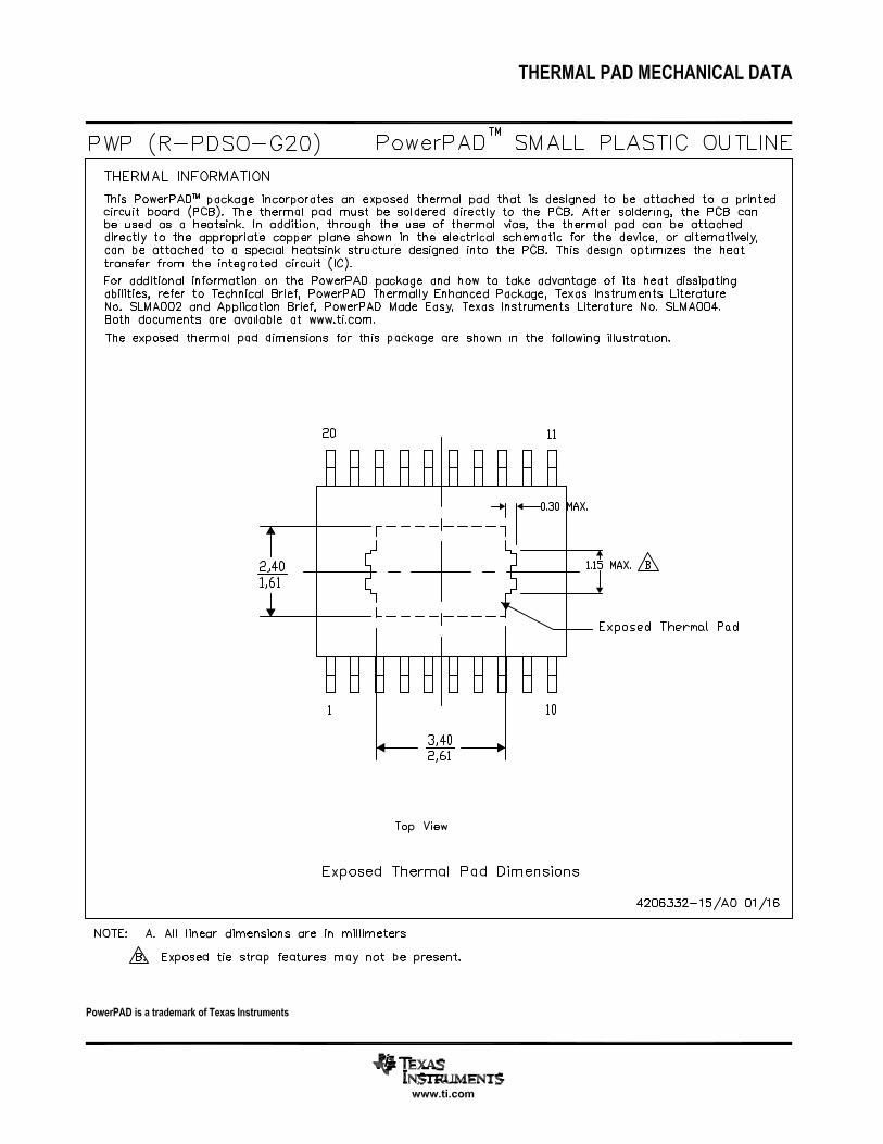
Thermal
Pad
3
TPS92638-Q1www.ti.com SLVSCK5B –SEPTEMBER 2014–REVISED MARCH 2015
Product Folder Links: TPS92638-Q1
Submit Documentation FeedbackCopyright © 2014–2015, Texas Instruments Incorporated
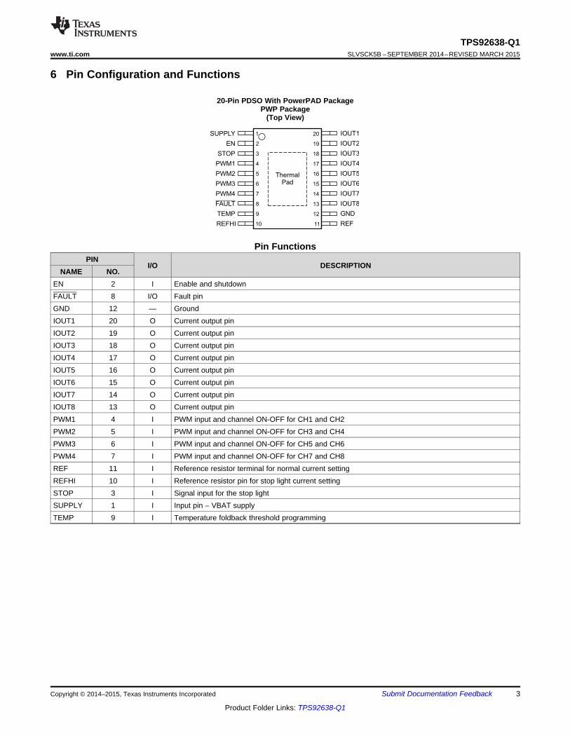
6 Pin Configuration and Functions
20-Pin PDSO With PowerPAD PackagePWP Package
(Top View)
Pin FunctionsPIN
I/O DESCRIPTIONNAME NO.
EN 2 I Enable and shutdownFAULT 8 I/O Fault pinGND 12 — GroundIOUT1 20 O Current output pinIOUT2 19 O Current output pinIOUT3 18 O Current output pinIOUT4 17 O Current output pinIOUT5 16 O Current output pinIOUT6 15 O Current output pinIOUT7 14 O Current output pinIOUT8 13 O Current output pinPWM1 4 I PWM input and channel ON-OFF for CH1 and CH2PWM2 5 I PWM input and channel ON-OFF for CH3 and CH4PWM3 6 I PWM input and channel ON-OFF for CH5 and CH6PWM4 7 I PWM input and channel ON-OFF for CH7 and CH8REF 11 I Reference resistor terminal for normal current settingREFHI 10 I Reference resistor pin for stop light current settingSTOP 3 I Signal input for the stop lightSUPPLY 1 I Input pin – VBAT supplyTEMP 9 I Temperature foldback threshold programming

4
TPS92638-Q1SLVSCK5B –SEPTEMBER 2014–REVISED MARCH 2015 www.ti.com
Product Folder Links: TPS92638-Q1
Submit Documentation Feedback Copyright © 2014–2015, Texas Instruments Incorporated
(1) Stresses beyond those listed under Absolute Maximum Ratings may cause permanent damage to the device. These are stress ratingsonly, which do not imply functional operation of the device at these or any other conditions beyond those indicated under RecommendedOperating Conditions. Exposure to absolute-maximum-rated conditions for extended periods may affect device reliability.
(2) All voltage values are with respect to GND.(3) Absolute maximum voltage 45 V for 200 ms
7 Specifications
7.1 Absolute Maximum Ratingsover operating free-air temperature range (unless otherwise noted) (1)
MIN MAX UNITSUPPLY, IOUTx, PWMx, EN,STOP Unregulated input (2) (3) –0.3 45 V
FAULT See (2) –0.3 22 VREF, REFHI, TEMP See (2) –0.3 7 VTJ Virtual junction temperature range –40 150 °CTA Operating ambient temperature range –40 125 °CTstg Storage temperature range –65 150 °C
(1) AEC Q100-002 indicates that HBM stressing shall be in accordance with the ANSI/ESDA/JEDEC JS-001 specification.
7.2 ESD RatingsVALUE UNIT
V(ESD) Electrostatic discharge
Human body model (HBM), per AEC Q100-002 (1) ±2000
VCharged device model(CDM), per AEC Q100-011
Corner pins (SUPPLY,IOUT1, REF and REFHI) ±750
Other pins ±500
7.3 Recommended Operating Conditionsover operating free-air temperature range (unless otherwise noted)
MIN NOM MAX UNITSUPPLY 5 40 V
VIH
EN, STOP 2 40VFAULT 2 20
PWMx 2 40
VIL
EN, STOP 0 0.7VFAULT 0 0.7
PWMx 0 0.7REF, REFHI, TEMP 0 5 V
TJ Operating junction temperature range –40 150 °C
(1) For more information about traditional and new thermal metrics, see the Semiconductor and IC Package Thermal Metrics applicationreport, SPRA953.
7.4 Thermal Information
THERMAL METRIC (1)TPS92638-Q1
UNITPWP (HTSSOP)20 PINS
RθJA Junction-to-ambient thermal resistance 37.8 °C/WRθJC(top) Junction-to-case (top) thermal resistance 25.2 °C/WRθJB Junction-to-board thermal resistance 21.7 °C/WψJT Junction-to-top characterization parameter 0.8 °C/WψJB Junction-to-board characterization parameter 21.5 °C/WRθJC(bot) Junction-to-case (bottom) thermal resistance 2.1 °C/W
5
TPS92638-Q1www.ti.com SLVSCK5B –SEPTEMBER 2014–REVISED MARCH 2015
Product Folder Links: TPS92638-Q1
Submit Documentation FeedbackCopyright © 2014–2015, Texas Instruments Incorporated
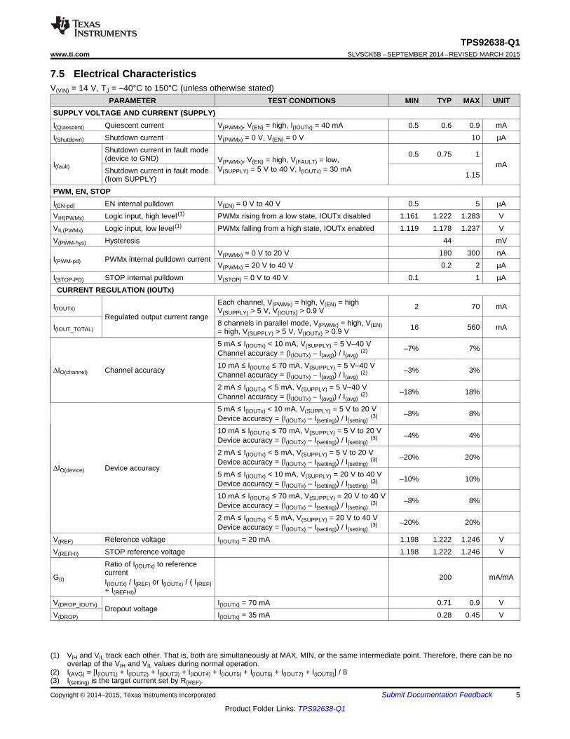
(1) VIH and VIL track each other. That is, both are simultaneously at MAX, MIN, or the same intermediate point. Therefore, there can be nooverlap of the VIH and VIL values during normal operation.
(2) I(AVG) = [I(IOUT1) + I(IOUT2) + I(IOUT3) + I(IOUT4) + I(IOUT5) + I(IOUT6) + I(IOUT7) + I(IOUT8)] / 8(3) I(setting) is the target current set by R(REF).
7.5 Electrical CharacteristicsV(VIN) = 14 V, TJ = –40°C to 150°C (unless otherwise stated)
PARAMETER TEST CONDITIONS MIN TYP MAX UNITSUPPLY VOLTAGE AND CURRENT (SUPPLY)I(Quiescent) Quiescent current V(PWMx), V(EN) = high, I(IOUTx) = 40 mA 0.5 0.6 0.9 mAI(Shutdown) Shutdown current V(PWMx) = 0 V, V(EN) = 0 V 10 µA
I(fault)
Shutdown current in fault mode(device to GND) V(PWMx), V(EN) = high, V(FAULT) = low,
V(SUPPLY) = 5 V to 40 V, I(IOUTx) = 30 mA
0.5 0.75 1mA
Shutdown current in fault mode(from SUPPLY) 1.15
PWM, EN, STOPI(EN-pd) EN internal pulldown V(EN) = 0 V to 40 V 0.5 5 µAVIH(PWMx) Logic input, high level (1) PWMx rising from a low state, IOUTx disabled 1.161 1.222 1.283 VVIL(PWMx) Logic input, low level (1) PWMx falling from a high state, IOUTx enabled 1.119 1.178 1.237 VV(PWM-hys) Hysteresis 44 mV
I(PWM-pd) PWMx internal pulldown currentV(PWMx) = 0 V to 20 V 180 300 nAV(PWMx) = 20 V to 40 V 0.2 2 µA
I(STOP-PD) STOP internal pulldown V(STOP) = 0 V to 40 V 0.1 1 µACURRENT REGULATION (IOUTx)
I(IOUTx)Regulated output current range
Each channel, V(PWMx) = high, V(EN) = highV(SUPPLY) > 5 V, V(IOUTx) > 0.9 V 2 70 mA
I(IOUT_TOTAL)8 channels in parallel mode, V(PWMx) = high, V(EN)= high, V(SUPPLY) > 5 V, V(IOUTx) > 0.9 V 16 560 mA
ΔIO(channel) Channel accuracy
5 mA ≤ I(IOUTx) < 10 mA, V(SUPPLY) = 5 V–40 VChannel accuracy = (I(IOUTx) – I(avg)) / I(avg)
(2) –7% 7%
10 mA ≤ I(IOUTx) ≤ 70 mA, V(SUPPLY) = 5 V–40 VChannel accuracy = (I(IOUTx) – I(avg)) / I(avg)
(2) –3% 3%
2 mA ≤ I(IOUTx) < 5 mA, V(SUPPLY) = 5 V–40 VChannel accuracy = (I(IOUTx) – I(avg)) / I(avg)
(2) –18% 18%
ΔIO(device) Device accuracy
5 mA ≤ I(IOUTx) < 10 mA, V(SUPPLY) = 5 V to 20 VDevice accuracy = (I(IOUTx) – I(setting)) / I(setting)
(3) –8% 8%
10 mA ≤ I(IOUTx) ≤ 70 mA, V(SUPPLY) = 5 V to 20 VDevice accuracy = (I(IOUTx) – I(setting)) / I(setting)
(3) –4% 4%
2 mA ≤ I(IOUTx) < 5 mA, V(SUPPLY) = 5 V to 20 VDevice accuracy = (I(IOUTx) – I(setting)) / I(setting)
(3) –20% 20%
5 mA ≤ I(IOUTx) < 10 mA, V(SUPPLY) = 20 V to 40 VDevice accuracy = (I(IOUTx) – I(setting)) / I(setting)
(3) –10% 10%
10 mA ≤ I(IOUTx) ≤ 70 mA, V(SUPPLY) = 20 V to 40 VDevice accuracy = (I(IOUTx) – I(setting)) / I(setting)
(3) –8% 8%
2 mA ≤ I(IOUTx) < 5 mA, V(SUPPLY) = 20 V to 40 VDevice accuracy = (I(IOUTx) – I(setting)) / I(setting)
(3) –20% 20%
V(REF) Reference voltage I(IOUTx) = 20 mA 1.198 1.222 1.246 VV(REFHI) STOP reference voltage 1.198 1.222 1.246 V
G(I)
Ratio of I(IOUTx) to referencecurrentI(IOUTx) / I(REF) or I(IOUTx) / ( I(REF)+ I(REFHI))
200 mA/mA
V(DROP_IOUTx) Dropout voltageI(IOUTx) = 70 mA 0.71 0.9 V
V(DROP) I(IOUTx) = 35 mA 0.28 0.45 V
6
TPS92638-Q1SLVSCK5B –SEPTEMBER 2014–REVISED MARCH 2015 www.ti.com
Product Folder Links: TPS92638-Q1
Submit Documentation Feedback Copyright © 2014–2015, Texas Instruments Incorporated
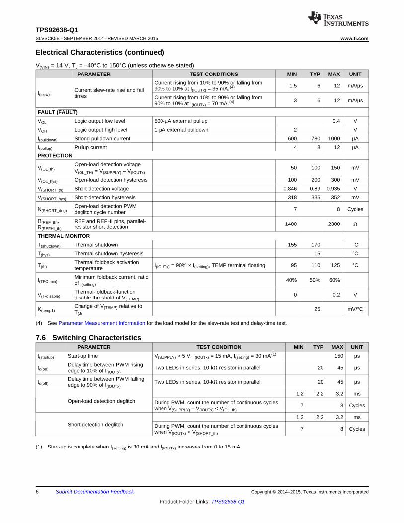
Electrical Characteristics (continued)V(VIN) = 14 V, TJ = –40°C to 150°C (unless otherwise stated)
PARAMETER TEST CONDITIONS MIN TYP MAX UNIT
(4) See Parameter Measurement Information for the load model for the slew-rate test and delay-time test.
I(slew)Current slew-rate rise and falltimes
Current rising from 10% to 90% or falling from90% to 10% at I(IOUTx) = 35 mA. (4) 1.5 6 12 mA/µs
Current rising from 10% to 90% or falling from90% to 10% at I(IOUTx) = 70 mA. (4) 3 6 12 mA/µs
FAULT (FAULT)VOL Logic output low level 500-µA external pullup 0.4 VVOH Logic output high level 1-µA external pulldown 2 VI(pulldown) Strong pulldown current 600 780 1000 µAI(pullup) Pullup current 4 8 12 µAPROTECTION
V(OL_th)Open-load detection voltageV(OL_TH) = V(SUPPLY) – V(IOUTx)
50 100 150 mV
V(OL_hys) Open-load detection hysteresis 100 200 300 mVV(SHORT_th) Short-detection voltage 0.846 0.89 0.935 VV(SHORT_hys) Short-detection hysteresis 318 335 352 mV
N(SHORT_deg)Open-load detection PWMdeglitch cycle number 7 8 Cycles
R(REF_th),R(REFHI_th)
REF and REFHI pins, parallel-resistor short detection 1400 2300 Ω
THERMAL MONITORT(shutdown) Thermal shutdown 155 170 °CT(hys) Thermal shutdown hysteresis 15 °C
T(th)Thermal foldback activationtemperature I(IOUTx) = 90% × I(setting), TEMP terminal floating 95 110 125 °C
I(TFC-min)Minimum foldback current, ratioof I(setting)
40% 50% 60%
V(T-disable)Thermal-foldback-functiondisable threshold of V(TEMP)
0 0.2 V
K(temp1)Change of V(TEMP) relative toT(J)
25 mV/°C
(1) Start-up is complete when I(setting) is 30 mA and I(IOUTx) increases from 0 to 15 mA.
7.6 Switching CharacteristicsPARAMETER TEST CONDITION MIN TYP MAX UNIT
t(startup) Start-up time V(SUPPLY) > 5 V, I(IOUTx) = 15 mA, I(setting) = 30 mA (1) 150 µs
td(on)Delay time between PWM risingedge to 10% of I(IOUTx)
Two LEDs in series, 10-kΩ resistor in parallel 20 45 µs
td(off)Delay time between PWM fallingedge to 90% of I(IOUTx)
Two LEDs in series, 10-kΩ resistor in parallel 20 45 µs
Open-load detection deglitch1.2 2.2 3.2 ms
During PWM, count the number of continuous cycleswhen V(SUPPLY) – V(IOUTx) < V(OL_th)
7 8 Cycles
Short-detection deglitch1.2 2.2 3.2 ms
During PWM, count the number of continuous cycleswhen V(IOUTx) < V(SHORT_th)
7 8 Cycles
Ambient Temperature (qC)
Cur
rent
(m
A)
-50 0 50 100 15034.55
34.6
34.65
34.7
34.75
34.8
34.85
34.9
34.95
35
35.05
D009
Ch1Ch2Ch3Ch4
Ch5Ch6Ch7Ch8
Ambient Temperature (qC)
Cur
rent
(m
A)
-50 0 50 100 15034.5
34.55
34.6
34.65
34.7
34.75
34.8
34.85
34.9
34.95
35
35.05
D010
Ch1Ch2Ch3Ch4
Ch5Ch6Ch7Ch8
Ambient Temperature (qC)
Cha
nnel
Acc
urac
y
-50 0 50 100 150-2%
-1%
0
1%
2%
D003
Ch1Ch2Ch3Ch4
Ch5Ch6Ch7Ch8
Ambient Temperature (qC)
Cha
nnel
Acc
urac
y
-50 0 50 100 150-2%
-1%
0
1%
2%
D004
Ch1Ch2Ch3Ch4
Ch5Ch6Ch7Ch8
Supply Voltage (V)
Cha
nnel
Acc
urac
y
0 5 10 15 20 25 30 35 40 45-2%
-1.5%
-1%
-0.5%
0
0.5%
1%
1.5%
2%
D005
Ch1Ch2Ch3Ch4
Ch5Ch6Ch7Ch8
Ambient Temperature (qC)
Cha
nnel
Acc
urac
y
-50 0 50 100 150-2%
-1%
0
1%
2%
D002
Ch1Ch2Ch3Ch4
Ch5Ch6Ch7Ch8
7
TPS92638-Q1www.ti.com SLVSCK5B –SEPTEMBER 2014–REVISED MARCH 2015
Product Folder Links: TPS92638-Q1
Submit Documentation FeedbackCopyright © 2014–2015, Texas Instruments Incorporated
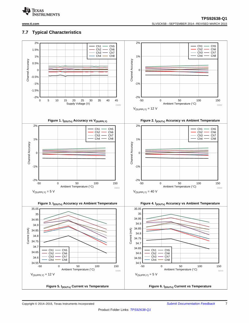
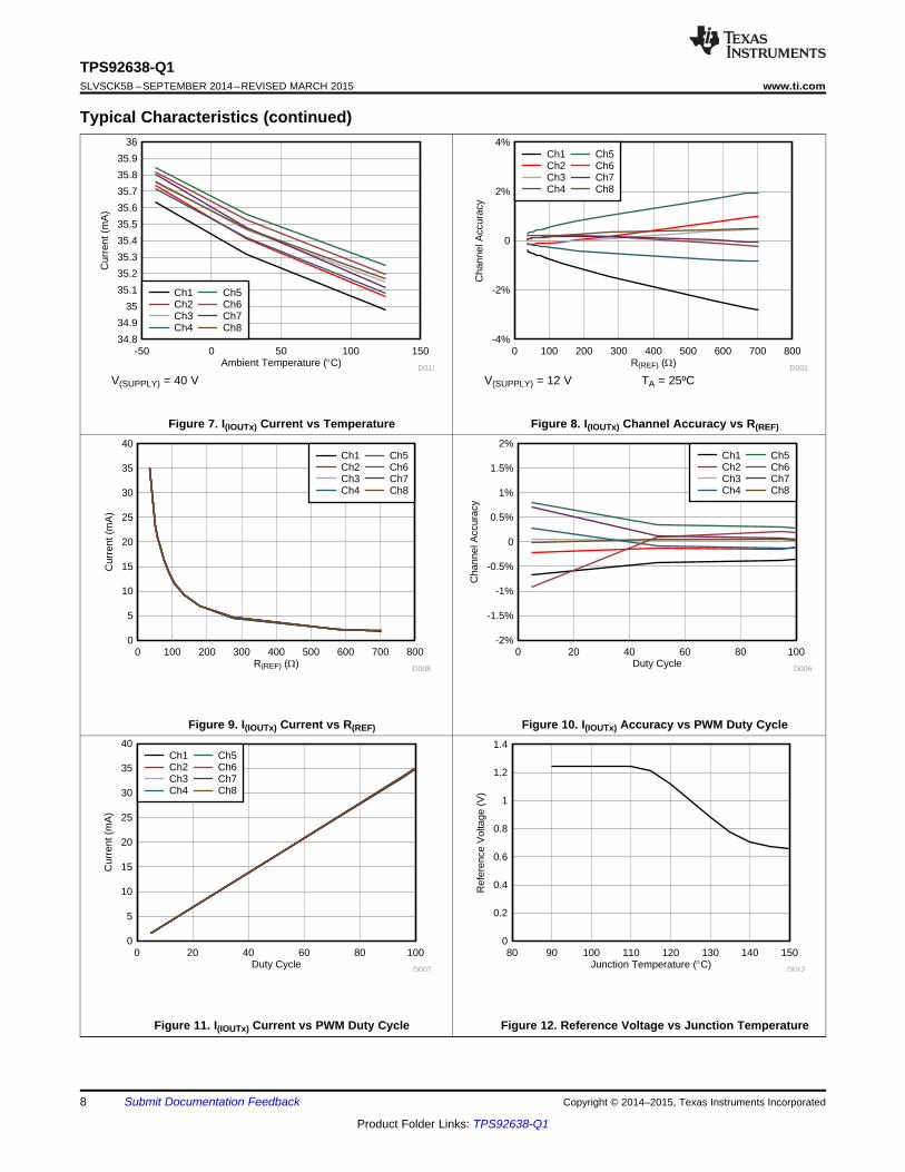
7.7 Typical Characteristics
Figure 1. I(IOUTx) Accuracy vs V(SUPPLY)
V(SUPPLY) = 12 V
Figure 2. I(IOUTx) Accuracy vs Ambient Temperature
V(SUPPLY) = 5 V
Figure 3. I(IOUTx) Accuracy vs Ambient Temperature
V(SUPPLY) = 40 V
Figure 4. I(IOUTx) Accuracy vs Ambient Temperature
V(SUPPLY) = 12 V
Figure 5. I(IOUTx) Current vs Temperature
V(SUPPLY) = 5 V
Figure 6. I(IOUTx) Current vs Temperature
Duty Cycle
Cur
rent
(m
A)
0 20 40 60 80 1000
5
10
15
20
25
30
35
40
D007
Ch1Ch2Ch3Ch4
Ch5Ch6Ch7Ch8
Junction Temperature (qC)
Ref
eren
ce V
olta
ge (
V)
80 90 100 110 120 130 140 1500
0.2
0.4
0.6
0.8
1
1.2
1.4
D012
R(REF) (:)
Cur
rent
(m
A)
0 100 200 300 400 500 600 700 8000
5
10
15
20
25
30
35
40
D008
Ch1Ch2Ch3Ch4
Ch5Ch6Ch7Ch8
Duty Cycle
Cha
nnel
Acc
urac
y
0 20 40 60 80 100-2%
-1.5%
-1%
-0.5%
0
0.5%
1%
1.5%
2%
D006
Ch1Ch2Ch3Ch4
Ch5Ch6Ch7Ch8
Ambient Temperature (qC)
Cur
rent
(m
A)
-50 0 50 100 15034.8
34.9
35
35.1
35.2
35.3
35.4
35.5
35.6
35.7
35.8
35.9
36
D011
Ch1Ch2Ch3Ch4
Ch5Ch6Ch7Ch8
R(REF) (:)
Cha
nnel
Acc
urac
y
0 100 200 300 400 500 600 700 800-4%
-2%
0
2%
4%
D001
Ch1Ch2Ch3Ch4
Ch5Ch6Ch7Ch8
8
TPS92638-Q1SLVSCK5B –SEPTEMBER 2014–REVISED MARCH 2015 www.ti.com
Product Folder Links: TPS92638-Q1
Submit Documentation Feedback Copyright © 2014–2015, Texas Instruments Incorporated
Typical Characteristics (continued)
V(SUPPLY) = 40 V
Figure 7. I(IOUTx) Current vs Temperature
V(SUPPLY) = 12 V TA = 25ºC
Figure 8. I(IOUTx) Channel Accuracy vs R(REF)
Figure 9. I(IOUTx) Current vs R(REF) Figure 10. I(IOUTx) Accuracy vs PWM Duty Cycle
Figure 11. I(IOUTx) Current vs PWM Duty Cycle Figure 12. Reference Voltage vs Junction Temperature
9
TPS92638-Q1www.ti.com SLVSCK5B –SEPTEMBER 2014–REVISED MARCH 2015
Product Folder Links: TPS92638-Q1
Submit Documentation FeedbackCopyright © 2014–2015, Texas Instruments Incorporated
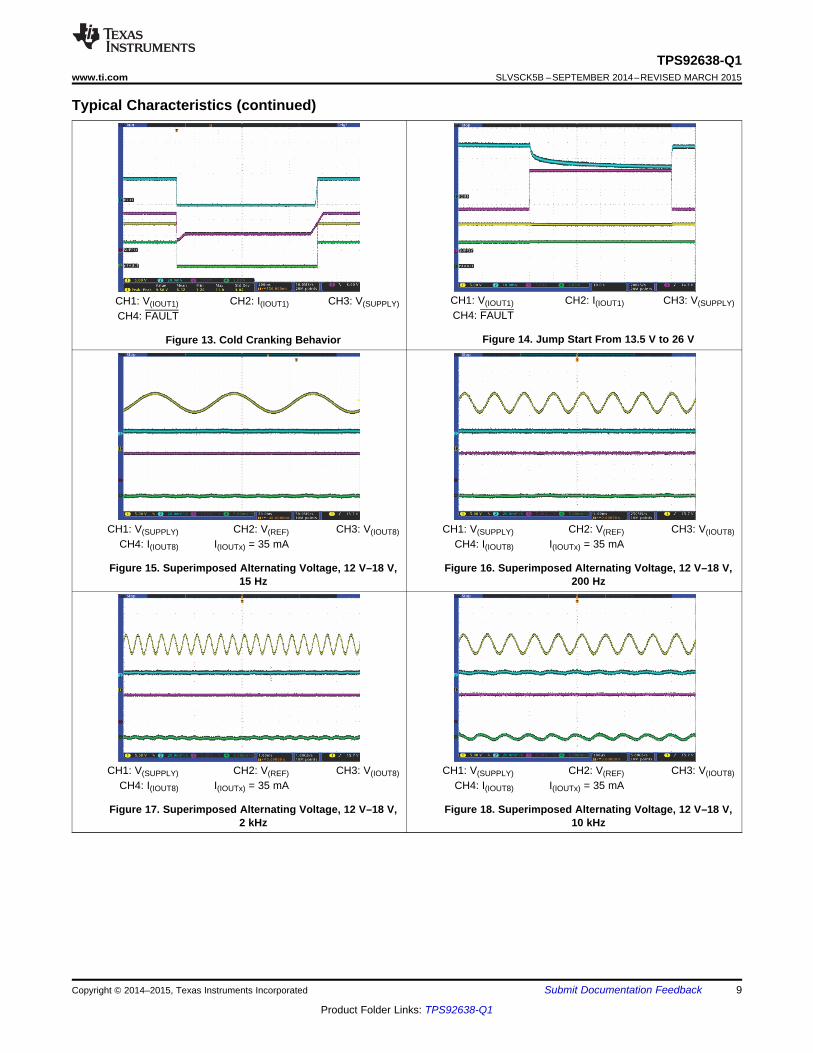
Typical Characteristics (continued)
CH1: V(IOUT1) CH2: I(IOUT1) CH3: V(SUPPLY)CH4: FAULT
Figure 13. Cold Cranking Behavior
CH1: V(IOUT1) CH2: I(IOUT1) CH3: V(SUPPLY)CH4: FAULT
Figure 14. Jump Start From 13.5 V to 26 V
CH1: V(SUPPLY) CH2: V(REF) CH3: V(IOUT8)CH4: I(IOUT8) I(IOUTx) = 35 mA
Figure 15. Superimposed Alternating Voltage, 12 V–18 V,15 Hz
CH1: V(SUPPLY) CH2: V(REF) CH3: V(IOUT8)CH4: I(IOUT8) I(IOUTx) = 35 mA
Figure 16. Superimposed Alternating Voltage, 12 V–18 V,200 Hz
CH1: V(SUPPLY) CH2: V(REF) CH3: V(IOUT8)CH4: I(IOUT8) I(IOUTx) = 35 mA
Figure 17. Superimposed Alternating Voltage, 12 V–18 V,2 kHz
CH1: V(SUPPLY) CH2: V(REF) CH3: V(IOUT8)CH4: I(IOUT8) I(IOUTx) = 35 mA
Figure 18. Superimposed Alternating Voltage, 12 V–18 V,10 kHz

10
TPS92638-Q1SLVSCK5B –SEPTEMBER 2014–REVISED MARCH 2015 www.ti.com
Product Folder Links: TPS92638-Q1
Submit Documentation Feedback Copyright © 2014–2015, Texas Instruments Incorporated
Typical Characteristics (continued)
CH1: V(SUPPLY) CH2: V(REF) CH3: V(IOUT8)CH4: I(IOUT8) I(IOUTx) = 35 mA
Figure 19. Superimposed Alternating Voltage, 12 V–18 V,20 kHz
CH1: V(SUPPLY) CH2: V(REF) CH3: V(IOUT8)CH4: I(IOUT8) I(IOUTx) = 35 mA
Figure 20. Superimposed Alternating Voltage, 12 V–18 V,30 kHz
CH1: V(IOUT1) CH2: I(IOUT1) CH3: V(SUPPLY)CH4: I(FAULT)
Figure 21. Transient Overvoltage (16 V – 18 V – 17 V – 16 V)
CH1: V(IOUT1) CH2: I(IOUT1) CH3: V(SUPPLY)CH4: I(FAULT)
Figure 22. Transient Undervoltage (10.8 V – 9 V – 10.8 V)
CH1: V(IOUT1) CH2: I(IOUT1) CH3: V(SUPPLY)CH4: I(FAULT)
Figure 23. Slow Decrease and Quick Increase
CH1: V(IOUT1) CH2: I(IOUT1) CH3: V(SUPPLY)CH4: I(FAULT)
Figure 24. Slow Decrease and Slow Increase

11
TPS92638-Q1www.ti.com SLVSCK5B –SEPTEMBER 2014–REVISED MARCH 2015
Product Folder Links: TPS92638-Q1
Submit Documentation FeedbackCopyright © 2014–2015, Texas Instruments Incorporated
Typical Characteristics (continued)
CH1: V(SUPPLY) CH2: V(FAULT) CH3: V(REF)CH4: I(IOUT8)
Figure 25. Slow Power Up (V(SUPPLY), V(EN), V(PWMx) RiseTogether From 0 V to 14 V by 0.2 V/s)
CH1: V(SUPPLY) CH2: V(FAULT) CH3: V(REF)CH4: I(IOUT8)
Figure 26. Slow Power Down (V(SUPPLY), V(EN), V(PWMx) FallTogether From 14 V to 0 V by 0.2 V/s)
CH1: V(PWM3) CH2: V(PWM4) CH3: V(REF)CH4: I(IOUT8) Duty cycle = 50% V(SUPPLY), V(EN) = 14 V
Figure 27. PWM Dimming, Dimming Frequency = 1000 Hz
CH1: V(REFHI) CH2: V(REF) CH3: I(IOUT1)CH4: I(IOUT8)
Figure 28. Load Transient, I(IOUTx) Increases From 35 mA to70 mA
CH1: V(REFHI) CH2: V(REF) CH3: I(IOUT1)CH4: I(IOUT8)
Figure 29. Load Transient, I(IOUTx) Decreases From 70 mA to35 mA
CH1: V(SUPPLY) CH2: V(REF) CH3: V(FAULT)I(IOUTx) = 35 mA
Figure 30. Line Transient, V(SUPPLY), V(EN), V(PWMx) RampFrom 9 V to 16 V to 9 V by 0.1 V/µs
SUPPLY
GND TEMP
REF
IOUTx
5.5 V
TPS92638-Q1
EN
V(bat)
0.7 V
17 Ω at 70 mA40 Ω at 30 mA
REFHI
STOP
PWM1
PWM3
PWM4
PWM2
FAULT
PWMX
IOUTX
ton toff
90%
10%
t1 t2 t3 t4 t5 t6
I1
I2
10kΩ
12
TPS92638-Q1SLVSCK5B –SEPTEMBER 2014–REVISED MARCH 2015 www.ti.com
Product Folder Links: TPS92638-Q1
Submit Documentation Feedback Copyright © 2014–2015, Texas Instruments Incorporated
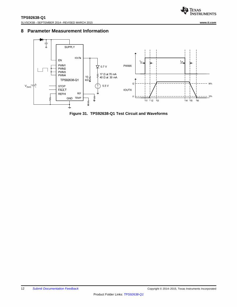
8 Parameter Measurement Information
Figure 31. TPS92638-Q1 Test Circuit and Waveforms
V(bat)
SUPPLY
Current Regulator
GND
FAULT
R(REF) CurrentReference
Control Logic
EN
REF
TEMP ThermalControl
R(REF1)
REFHI
STOP
PWMx
IOUT1
IOUT2
IOUT3
IOUT4
IOUT5
IOUT6
IOUT7
IOUT8
13
TPS92638-Q1www.ti.com SLVSCK5B –SEPTEMBER 2014–REVISED MARCH 2015
Product Folder Links: TPS92638-Q1
Submit Documentation FeedbackCopyright © 2014–2015, Texas Instruments Incorporated
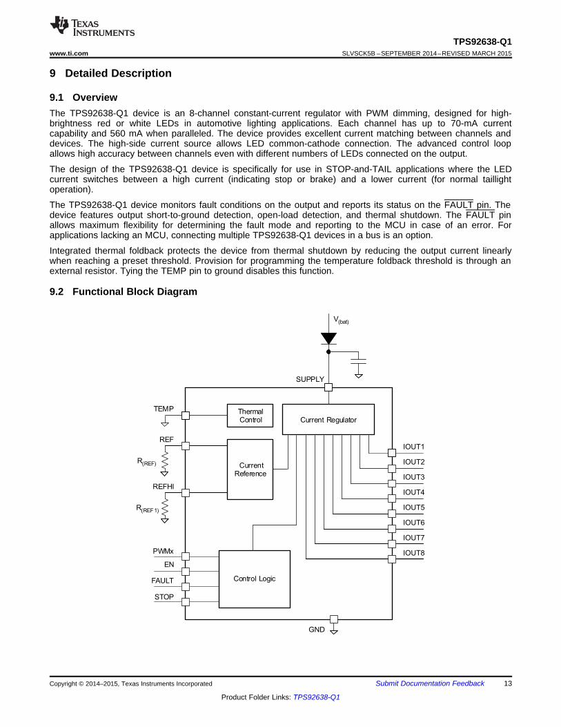
9 Detailed Description
9.1 OverviewThe TPS92638-Q1 device is an 8-channel constant-current regulator with PWM dimming, designed for high-brightness red or white LEDs in automotive lighting applications. Each channel has up to 70-mA currentcapability and 560 mA when paralleled. The device provides excellent current matching between channels anddevices. The high-side current source allows LED common-cathode connection. The advanced control loopallows high accuracy between channels even with different numbers of LEDs connected on the output.
The design of the TPS92638-Q1 device is specifically for use in STOP-and-TAIL applications where the LEDcurrent switches between a high current (indicating stop or brake) and a lower current (for normal taillightoperation).
The TPS92638-Q1 device monitors fault conditions on the output and reports its status on the FAULT pin. Thedevice features output short-to-ground detection, open-load detection, and thermal shutdown. The FAULT pinallows maximum flexibility for determining the fault mode and reporting to the MCU in case of an error. Forapplications lacking an MCU, connecting multiple TPS92638-Q1 devices in a bus is an option.
Integrated thermal foldback protects the device from thermal shutdown by reducing the output current linearlywhen reaching a preset threshold. Provision for programming the temperature foldback threshold is through anexternal resistor. Tying the TEMP pin to ground disables this function.
9.2 Functional Block Diagram
ref (I) ref (I)(IOUTx-STOP)
(REFHI) (REF)
ref (I)(REFHI)
ref (I)(IOUTx-STOP)
(REF)
V G V GI
R R
V GR
V GI
R
´ ´
= +
´
=
´
-
ref (I)(OUTx-TAIL)
(REF)
ref (I)(REF)
(OUTx-TAIL)
V GI
R
V GR
I
´
=
´
=
14
TPS92638-Q1SLVSCK5B –SEPTEMBER 2014–REVISED MARCH 2015 www.ti.com
Product Folder Links: TPS92638-Q1
Submit Documentation Feedback Copyright © 2014–2015, Texas Instruments Incorporated
9.3 Feature Description
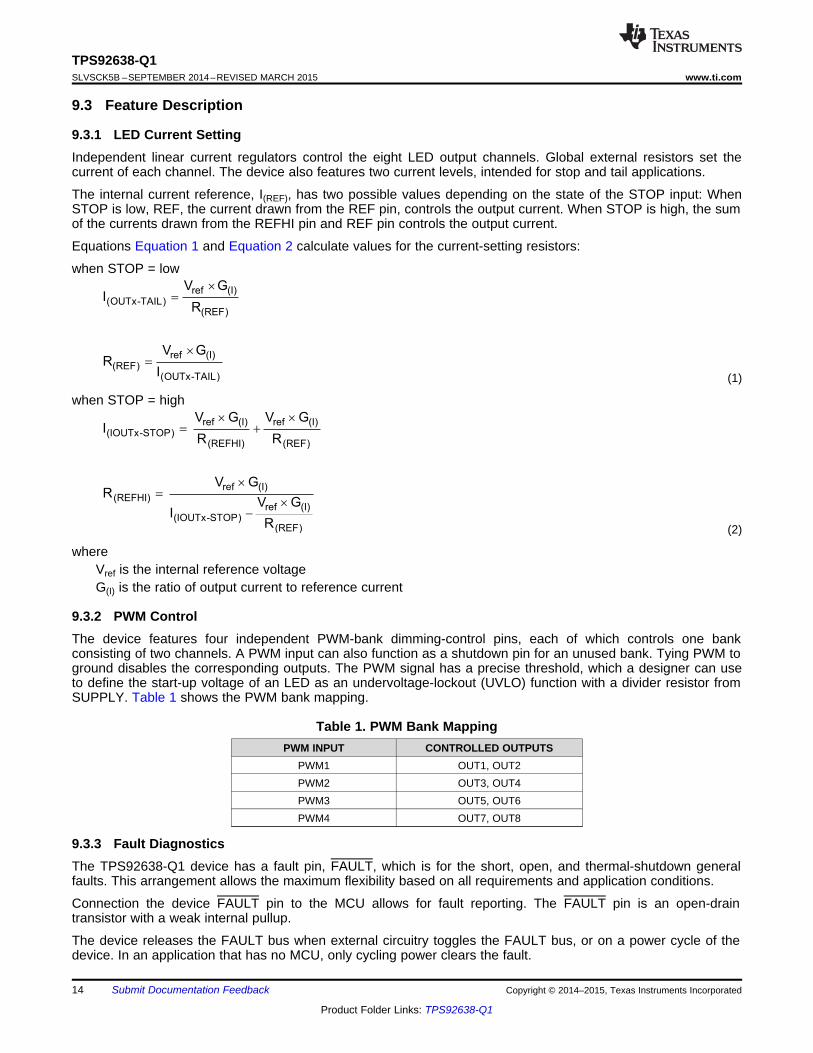
9.3.1 LED Current SettingIndependent linear current regulators control the eight LED output channels. Global external resistors set thecurrent of each channel. The device also features two current levels, intended for stop and tail applications.
The internal current reference, I(REF), has two possible values depending on the state of the STOP input: WhenSTOP is low, REF, the current drawn from the REF pin, controls the output current. When STOP is high, the sumof the currents drawn from the REFHI pin and REF pin controls the output current.
Equations Equation 1 and Equation 2 calculate values for the current-setting resistors:
when STOP = low
(1)
when STOP = high
(2)
whereVref is the internal reference voltageG(I) is the ratio of output current to reference current
9.3.2 PWM ControlThe device features four independent PWM-bank dimming-control pins, each of which controls one bankconsisting of two channels. A PWM input can also function as a shutdown pin for an unused bank. Tying PWM toground disables the corresponding outputs. The PWM signal has a precise threshold, which a designer can useto define the start-up voltage of an LED as an undervoltage-lockout (UVLO) function with a divider resistor fromSUPPLY. Table 1 shows the PWM bank mapping.
Table 1. PWM Bank MappingPWM INPUT CONTROLLED OUTPUTS
PWM1 OUT1, OUT2PWM2 OUT3, OUT4PWM3 OUT5, OUT6PWM4 OUT7, OUT8
9.3.3 Fault DiagnosticsThe TPS92638-Q1 device has a fault pin, FAULT, which is for the short, open, and thermal-shutdown generalfaults. This arrangement allows the maximum flexibility based on all requirements and application conditions.
Connection the device FAULT pin to the MCU allows for fault reporting. The FAULT pin is an open-draintransistor with a weak internal pullup.
The device releases the FAULT bus when external circuitry toggles the FAULT bus, or on a power cycle of thedevice. In an application that has no MCU, only cycling power clears the fault.

Fault removed
FAULT
SUPPLYand EN
FaultyChannel
OtherChannels
PWM
LEDOpen2 ms
LEDShort
to GND2 ms
LED Open7-PWM Cycles
LED Short7 PWM Cycles
15
TPS92638-Q1www.ti.com SLVSCK5B –SEPTEMBER 2014–REVISED MARCH 2015
Product Folder Links: TPS92638-Q1
Submit Documentation FeedbackCopyright © 2014–2015, Texas Instruments Incorporated
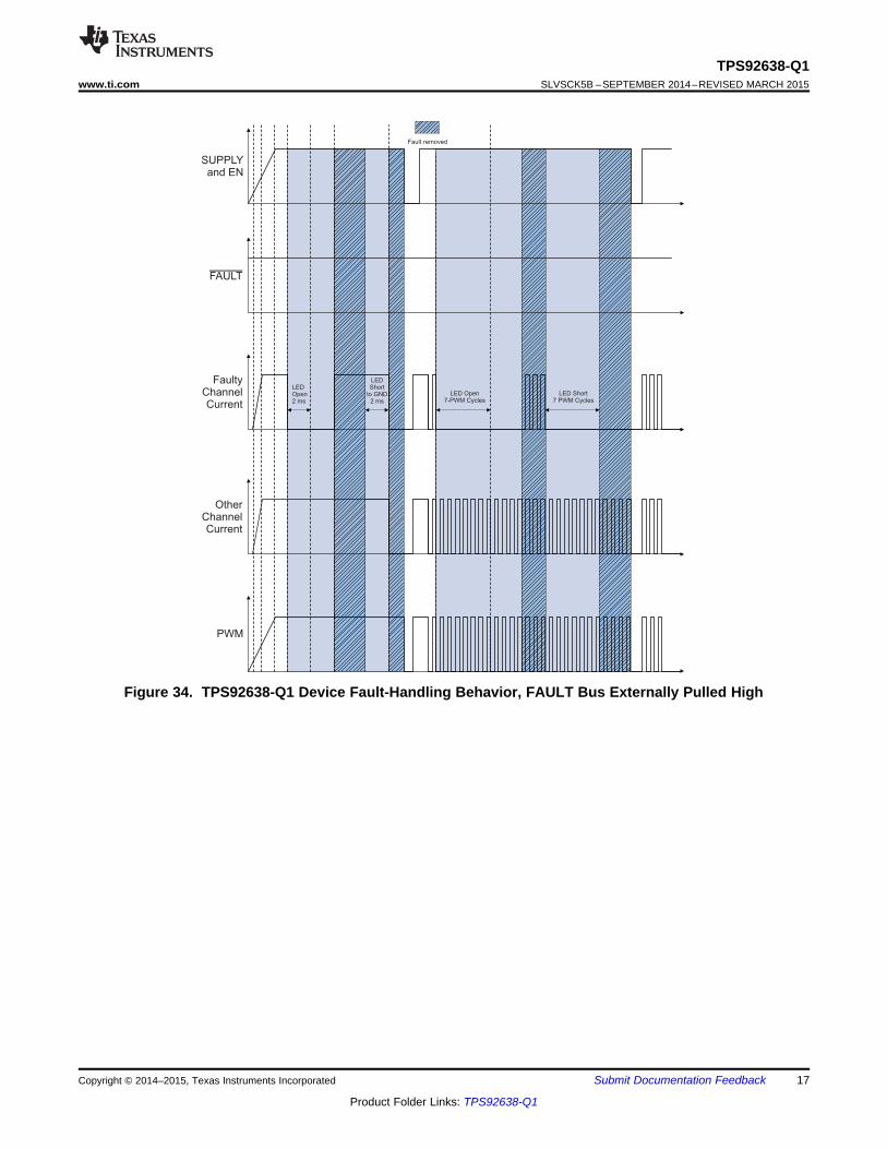
The following faults result in the FAULT pin going low: thermal shutdown, open load, or output short circuit. Forthermal shutdown and open LED, release of the FAULT pin occurs when the thermal shutdown or open-LEDcondition no longer exists. For other faults, the FAULT pin remains low even after the condition does not exist,and clearing is only possible by toggling FAULT or by power cycling of the device.
Figure 32. TPS92638-Q1 Device Fault-Handling Behavior, FAULT Bus Floating
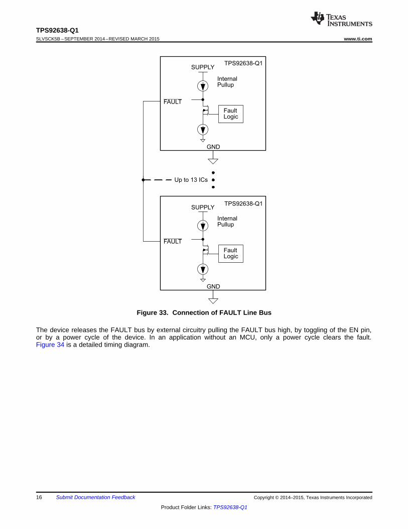
The design of an application with no MCU allows the connecting together of up to 15 TPS92638-Q1 FAULT pins.When one or more devices have errors, their corresponding FAULT pins go low, thus pulling down the connectedFAULT bus and shutting down all device outputs. Figure 33 illustrates the FAULT line bus connection.
SUPPLY
GND
FAULT
TPS92638-Q1
InternalPullup
FaultLogic
SUPPLY
GND
FAULT
TPS92638-Q1
InternalPullup
FaultLogic
Up to 13 ICs
16
TPS92638-Q1SLVSCK5B –SEPTEMBER 2014–REVISED MARCH 2015 www.ti.com
Product Folder Links: TPS92638-Q1
Submit Documentation Feedback Copyright © 2014–2015, Texas Instruments Incorporated
Figure 33. Connection of FAULT Line Bus
The device releases the FAULT bus by external circuitry pulling the FAULT bus high, by toggling of the EN pin,or by a power cycle of the device. In an application without an MCU, only a power cycle clears the fault.Figure 34 is a detailed timing diagram.
Fault removed
FAULT
SUPPLYand EN
FaultyChannelCurrent
OtherChannelCurrent
PWM
LEDOpen2 ms
LEDShort
to GND2 ms
LED Open7-PWM Cycles
LED Short7 PWM Cycles
17
TPS92638-Q1www.ti.com SLVSCK5B –SEPTEMBER 2014–REVISED MARCH 2015
Product Folder Links: TPS92638-Q1
Submit Documentation FeedbackCopyright © 2014–2015, Texas Instruments Incorporated
Figure 34. TPS92638-Q1 Device Fault-Handling Behavior, FAULT Bus Externally Pulled High
18
TPS92638-Q1SLVSCK5B –SEPTEMBER 2014–REVISED MARCH 2015 www.ti.com
Product Folder Links: TPS92638-Q1
Submit Documentation Feedback Copyright © 2014–2015, Texas Instruments Incorporated
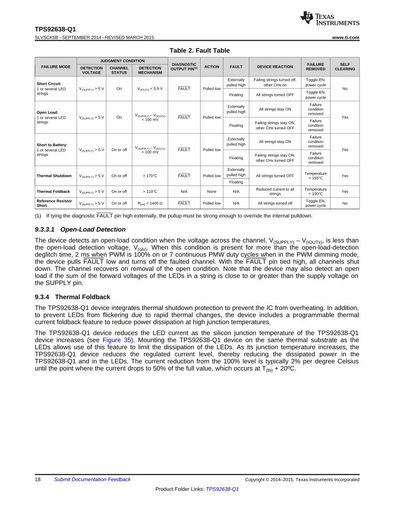
(1) If tying the diagnostic FAULT pin high externally, the pullup must be strong enough to override the internal pulldown.
Table 2. Fault Table
FAILURE MODEJUDGMENT CONDITION
DIAGNOSTICOUTPUT PIN (1) ACTION FAULT DEVICE REACTION FAILURE
REMOVEDSELF
CLEARINGDETECTIONVOLTAGE
CHANNELSTATUS
DETECTIONMECHANISM
Short Circuit:1 or several LEDstrings
V(SUPPLY) > 5 V On V(IOUTx) < 0.9 V FAULT Pulled low
Externallypulled high
Failing strings turned off,other CHs on
Toggle EN,power cycle
NoFloating All strings turned OFF
Toggle EN,power cycle
Open Load:1 or several LEDstrings
V(SUPPLY) > 5 V On V(SUPPLY) – V(IOUTx)< 100 mV FAULT Pulled low
Externallypulled high
All strings stay ONFailure
conditionremoved
Yes
FloatingFailing strings stay ON,other CHs turned OFF
Failureconditionremoved
Short to Battery:1 or several LEDstrings
V(SUPPLY) > 5 V On or off V(SUPPLY) – V(IOUTx)< 100 mV FAULT Pulled low
Externallypulled high
All strings stay ONFailure
conditionremoved
Yes
FloatingFailing strings stay ON,other CHs turned OFF
Failureconditionremoved
Thermal Shutdown V(SUPPLY) > 5 V On or off > 170°C FAULT Pulled lowExternallypulled high All strings turned OFF Temperature
< 155°C YesFloating
Thermal Foldback V(SUPPLY) > 5 V On or off > 110°C N/A None N/A Reduced current to allstrings
Temperature< 100°C Yes
Reference ResistorShort V(SUPPLY) > 5 V On or off R(ref) < 1400 Ω FAULT Pulled low N/A All strings turned off Toggle EN,
power cycle No
9.3.3.1 Open-Load DetectionThe device detects an open-load condition when the voltage across the channel, V(SUPPLY) – V(IOUTx), is less thanthe open-load detection voltage, V(olv). When this condition is present for more than the open-load-detectiondeglitch time, 2 ms when PWM is 100% on or 7 continuous PMW duty cycles when in the PWM dimming mode,the device pulls FAULT low and turns off the faulted channel. With the FAULT pin tied high, all channels shutdown. The channel recovers on removal of the open condition. Note that the device may also detect an openload if the sum of the forward voltages of the LEDs in a string is close to or greater than the supply voltage onthe SUPPLY pin.
9.3.4 Thermal FoldbackThe TPS92638-Q1 device integrates thermal shutdown protection to prevent the IC from overheating. In addition,to prevent LEDs from flickering due to rapid thermal changes, the device includes a programmable thermalcurrent foldback feature to reduce power dissipation at high junction temperatures.
The TPS92638-Q1 device reduces the LED current as the silicon junction temperature of the TPS92638-Q1device increases (see Figure 35). Mounting the TPS92638-Q1 device on the same thermal substrate as theLEDs allows use of this feature to limit the dissipation of the LEDs. As its junction temperature increases, theTPS92638-Q1 device reduces the regulated current level, thereby reducing the dissipated power in theTPS92638-Q1 and in the LEDs. The current reduction from the 100% level is typically 2% per degree Celsiusuntil the point where the current drops to 50% of the full value, which occurs at T(th) + 20ºC.

Thermal Foldback Temperature (qC)
TE
MP
Pin
Vol
tage
(V
)
0 25 50 75 100 125 1500
0.2
0.4
0.6
0.8
1
1.2
1.4
1.6
1.8
2
D004
(th) (TEMP)T 121.7 C/V V 228.32 C= - ° ´ + °
Out
put C
urre
nt in
an
LED
Str
ing
T(shutdown)T(th)
I(setting)
90%
50%
2% of I(setting) per ºC
T(th) + 20°C
19
TPS92638-Q1www.ti.com SLVSCK5B –SEPTEMBER 2014–REVISED MARCH 2015
Product Folder Links: TPS92638-Q1
Submit Documentation FeedbackCopyright © 2014–2015, Texas Instruments Incorporated
Figure 35. Thermal Foldback
Above this temperature, the device maintains the current at the 50% current level until the junction temperaturereaches the overtemperature shutdown threshold, T(shutdown). Changing the voltage on the TEMP pin adjusts thetemperature at which the current reduction begins. With TEMP left open, the definition of thermal monitoractivation temperature is the temperature at which the current reduction begins, T(th). The specification of T(th) inthe Electrical Characteristics table is at the 90% current level. T(th) increases as the voltage at the TEMP pin,V(TEMP), decreases. Equation 3 provides an approximate calculation of T(th).
(3)
Figure 36. TEMP Pin Voltage vs Thermal Foldback Temperature
A resistor connected between TEMP and GND reduces V(TEMP) and increases T(th). A resistor connected betweenTEMP and a reference supply greater than 1 V increases V(TEMP) and reduces T(th).

Thermal Foldback Temperature (ºC)
Pul
lup
or P
ulld
own
Res
isto
r (k:
)
20 40 60 80 100 120 140 1600
20
40
60
80
100
D005
V(res)0 V3.3 V5 V
20
TPS92638-Q1SLVSCK5B –SEPTEMBER 2014–REVISED MARCH 2015 www.ti.com
Product Folder Links: TPS92638-Q1
Submit Documentation Feedback Copyright © 2014–2015, Texas Instruments Incorporated
Figure 37. Pullup and Pulldown Resistors vs T(th)
Figure 37 shows how the nominal value of the thermal monitor activation temperature varies with the voltage atTEMP and with a resistor R(TEMP), either connected to GND or pulled up to 3 V or to 5 V.
In extreme cases, if the junction temperature exceeds the overtemperature limit, T(shutdown), the device disables allregulators. Temperature monitoring continues, and the device re-activates the regulators, when the temperaturedrops below the specified hysteresis threshold.
Note that it is possible for the TPS92638-Q1 device to transition rapidly between thermal shutdown and normaloperation. This can happen if the thermal mass attached to the exposed thermal pad is small and T(th) is tooclose to the shutdown temperature. The period of oscillation depends on T(th), the dissipated power, the thermalmass of any heatsink present, and the ambient temperature.
9.4 Device Functional ModesThe functional modes of the TPS92638-Q1 device are operational and non-operational. The device operatesnormally when V(SUPPLY) is at least 5 V and not greater than 40 V.

(I)(REF) (REF)
(STOP)
G 200R V 1.222 6.11 k
I 0.04= ´ = ´ = W
Battery
Tail
TLC555-Q1
VDD
OUT
SUPPLY
GND
TEMP
REF
IOUT1
FAULT
IOUT2
IOUT3
V(bat)
REFHI
IOUT4
IOUT5
IOUT6
IOUT7
IOUT8
STOP
EN
R(TEMP)
R(REF)
TPS92638-Q1
PWM1
PWM2
PWM3
PWM4
21
TPS92638-Q1www.ti.com SLVSCK5B –SEPTEMBER 2014–REVISED MARCH 2015
Product Folder Links: TPS92638-Q1
Submit Documentation FeedbackCopyright © 2014–2015, Texas Instruments Incorporated
10 Application and Implementation
NOTEInformation in the following applications sections is not part of the TI componentspecification, and TI does not warrant its accuracy or completeness. TI’s customers areresponsible for determining suitability of components for their purposes. Customers shouldvalidate and test their design implementation to confirm system functionality.
10.1 Application InformationThe following discussion includes several applications showing how to implement the TPS92638-Q1 device forautomotive lighting such as stop lights and taillights. Some of the examples demonstrate implementation of thefault bus function or detail use of the device for higher-current applications.
10.2 Typical Applications
10.2.1 PWM Dimming by BankThe TPS92638-Q1 device provides four PWM banks for output dimming. A TLC555-Q1 PWM generator can beused on the to avoid the use of an MCU.
Figure 38. Schematic for PWM Dimming by Bank
10.2.1.1 Design Requirements
(1) I(TAIL) = tail light curent per channel; I(STOP) = stop light current perchannel.
DESIGN PARAMETER EXAMPLE VALUEI(TAIL)
(1) 20 mAI(STOP)
(1) 40 mA
10.2.1.2 Detailed Design ProcedureThe design uses the R(REF) reference resistor to set the maximum output current, and the TLC555-Q1 sets thePWM duty cycle to control the dimming ratio.
(4)

(TAIL)
(STOP)
I 0.02Duty cycle 0.5 50%
I 0.04= = = =
22
TPS92638-Q1SLVSCK5B –SEPTEMBER 2014–REVISED MARCH 2015 www.ti.com
Product Folder Links: TPS92638-Q1
Submit Documentation Feedback Copyright © 2014–2015, Texas Instruments Incorporated
(5)
10.2.1.3 Application Performance Plots
SUPPLY = EN = 14 V PWM freq. = 1 kHz Duty cycle = 50%CH1: PWM1 CH2: PWM2 CH3: VrefCH4: IOUT8
Figure 39. PWM Dimming by Bank, PWM1, PWM2, AnalogReference and Output Current
SUPPLY = EN = 14 V PWM freq. = 1 kHz Duty cycle = 50%CH1: PWM3 CH2: PWM4 CH3: VrefCH4: IOUT8
Figure 40. PWM Dimming by Bank, PWM3, PWM4, AnalogReference and Output Current
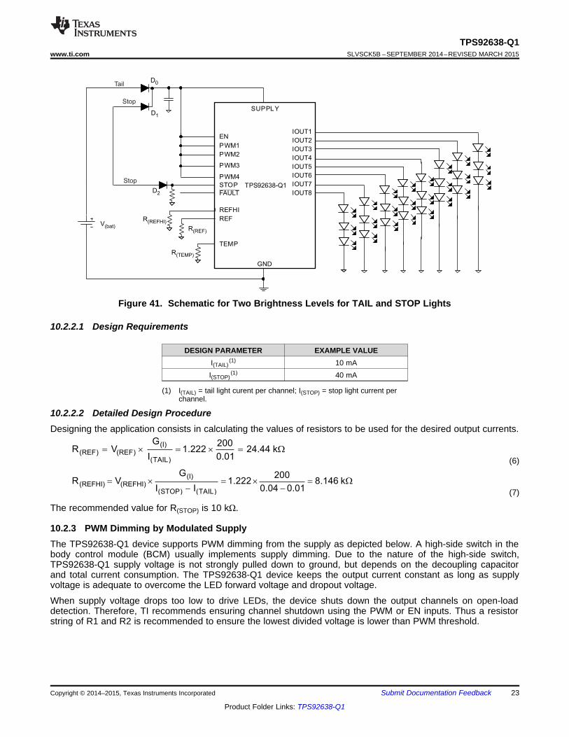
10.2.2 Two Brightness Levels for TAIL and STOP LightsFor a typical TAIL and STOP application, implementation using the TPS92638-Q1 device with an integratedSTOP and TAIL function is easy. The following schematic depicts the application circuit. In a typical application,two independent sources, namely Tail and Stop, power the stop and tail lights. Using blocking diodes D0 and D1with the TPS92638-Q1 device allows merging the STOP and TAIL functions, powered by a single supply.Blocking diode D2 protects the STOP pin during a reverse battery scenario. The STOP pin has an internalpulldown resistor to ensure a low state when STOP is not active.
(I)(REFHI) (REFHI)
(STOP) (TAIL)
G 200R V 1.222 8.146 k
I I 0.04 0.01= ´ = ´ = W
- -
(I)(REF) (REF)
(TAIL)
G 200R V 1.222 24.44 k
I 0.01= ´ = ´ = W
SUPPLY
GND
TEMP
REF
IOUT1
FAULT
IOUT2
IOUT3
TPS92638-Q1
V(bat)
REFHI
IOUT4
IOUT5
IOUT6
IOUT7
IOUT8
STOP
PWM4
PWM3
PWM2
PWM1
EN
D0
D1
D2
R(REFHI)
R(TEMP)
R(REF)
Stop
Stop
Tail
23
TPS92638-Q1www.ti.com SLVSCK5B –SEPTEMBER 2014–REVISED MARCH 2015
Product Folder Links: TPS92638-Q1
Submit Documentation FeedbackCopyright © 2014–2015, Texas Instruments Incorporated
Figure 41. Schematic for Two Brightness Levels for TAIL and STOP Lights
10.2.2.1 Design Requirements
(1) I(TAIL) = tail light curent per channel; I(STOP) = stop light current perchannel.
DESIGN PARAMETER EXAMPLE VALUEI(TAIL)
(1) 10 mAI(STOP)
(1) 40 mA
10.2.2.2 Detailed Design ProcedureDesigning the application consists in calculating the values of resistors to be used for the desired output currents.
(6)
(7)
The recommended value for R(STOP) is 10 kΩ.
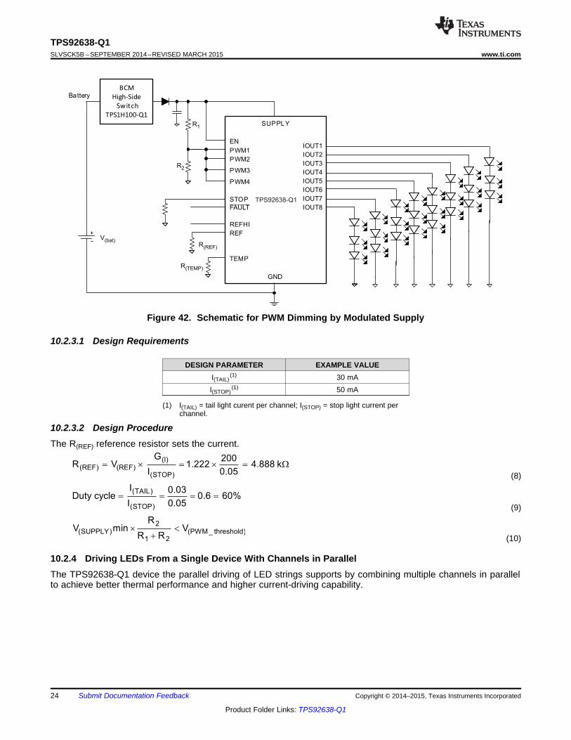
10.2.3 PWM Dimming by Modulated SupplyThe TPS92638-Q1 device supports PWM dimming from the supply as depicted below. A high-side switch in thebody control module (BCM) usually implements supply dimming. Due to the nature of the high-side switch,TPS92638-Q1 supply voltage is not strongly pulled down to ground, but depends on the decoupling capacitorand total current consumption. The TPS92638-Q1 device keeps the output current constant as long as supplyvoltage is adequate to overcome the LED forward voltage and dropout voltage.
When supply voltage drops too low to drive LEDs, the device shuts down the output channels on open-loaddetection. Therefore, TI recommends ensuring channel shutdown using the PWM or EN inputs. Thus a resistorstring of R1 and R2 is recommended to ensure the lowest divided voltage is lower than PWM threshold.
2(SUPPLY) (PWM_ threshold)
1 2
RV min V
R R´ <
+
(TAIL)
(STOP)
I 0.03Duty cycle 0.6 60%
I 0.05= = = =
(I)(REF) (REF)
(STOP)
G 200R V 1.222 4.888 k
I 0.05= ´ = ´ = W
BatteryBCM
High-Side
Switch
TPS1H100-Q1
R1
R2
SUPPLY
GND
TEMP
REF
IOUT1
FAULT
IOUT2
IOUT3
V(bat)
REFHI
IOUT4
IOUT5
IOUT6
IOUT7
IOUT8
STOP
PWM4
PWM3
PWM2
PWM1
EN
R(TEMP)
R(REF)
TPS92638-Q1
24
TPS92638-Q1SLVSCK5B –SEPTEMBER 2014–REVISED MARCH 2015 www.ti.com
Product Folder Links: TPS92638-Q1
Submit Documentation Feedback Copyright © 2014–2015, Texas Instruments Incorporated
Figure 42. Schematic for PWM Dimming by Modulated Supply
10.2.3.1 Design Requirements
(1) I(TAIL) = tail light curent per channel; I(STOP) = stop light current perchannel.
DESIGN PARAMETER EXAMPLE VALUEI(TAIL)
(1) 30 mAI(STOP)
(1) 50 mA
10.2.3.2 Design ProcedureThe R(REF) reference resistor sets the current.
(8)
(9)
(10)
10.2.4 Driving LEDs From a Single Device With Channels in ParallelThe TPS92638-Q1 device the parallel driving of LED strings supports by combining multiple channels in parallelto achieve better thermal performance and higher current-driving capability.

(I)(REF) (REF)
(TAIL) (channel)
G 200R V 1.222 16.29 k
I / N 0.03 / 2= ´ = ´ = W
Stop
GND
TEMP
REF
IOUT1
FAULT
IOUT2
IOUT3
TPS92638-Q1
V(bat)
REFHI
IOUT4
IOUT5
IOUT6
IOUT7
IOUT8
STOP
EN
R(REFHI)
R(TEMP)
R(REF)
SUPPLY
Battery
PWM1
PWM2
PWM3
PWM4
25
TPS92638-Q1www.ti.com SLVSCK5B –SEPTEMBER 2014–REVISED MARCH 2015
Product Folder Links: TPS92638-Q1
Submit Documentation FeedbackCopyright © 2014–2015, Texas Instruments Incorporated
Figure 43. Schematic for Driving With a Single Device Using Parallel Channels
10.2.4.1 Design Requirements
(1) I(TAIL) = tail light curent per channel; I(STOP) = stop light current perchannel.
DESIGN PARAMETER EXAMPLE VALUEI(TAIL)
(1) 30 mAI(STOP)
(1) 100 mA
10.2.4.2 Design ProcedureThe R(REF) and R(REFHI) reference resistors set the current. R(REF) sets the tail current, and R(REF) and R(REFHI) setthe stop current.
(11)
(12)
10.2.5 Driving LEDs From Multiple Devices With Channels in ParallelFor design flexibility, there is also support for using multiple TPS92638-Q1 devices in parallel driving betweendifferent devices. The following diagram shows a combination that uses both devices and channels in parallel todrive high-current loads.

Stop
SUPPLY
GND
TEMP
REF
IOUT1
FAULT
IOUT2
IOUT3
TPS92638-Q1
V(bat)
REFHI
IOUT4
IOUT5
IOUT6
IOUT7
IOUT8
STOP
EN
R(REFH)
R(TEMP)
R(REF)
SUPPLY
GND
TEMP
REF
IOUT1
FAULT
IOUT2
IOUT3
TPS92638-Q1
REFHI
IOUT4
IOUT5
IOUT6
IOUT7
IOUT8
STOP
EN
R(REFHI)
R(REF)
R(TEMP)
PWM1
PWM2
PWM3
PWM4
PWM1
PWM2
PWM3
PWM4
Battery
26
TPS92638-Q1SLVSCK5B –SEPTEMBER 2014–REVISED MARCH 2015 www.ti.com
Product Folder Links: TPS92638-Q1
Submit Documentation Feedback Copyright © 2014–2015, Texas Instruments Incorporated
Figure 44. Schematic for Driving With Multiple Devices Using Parallel Channels
10.2.5.1 Design Requirements
(1) I(TAIL) = tail light curent per channel; I(STOP) = stop light current perchannel.
DESIGN PARAMETER EXAMPLE VALUEI(TAIL)
(1) 60 mAI(STOP)
(1) 200 mA
10.2.5.2 Design ProcedureThe R(REFHI) and R(REF) reference resistors set the current. R(REF) by itself sets the tail current. R(REF) and R(REFHI)together set the stop current. In different applications, reference resistors can be set to different values fordifferent devices to achieve current flexibility. In this document, for simplicity, the application sets the samereference current in both devices.
( )(I)
(REFHI) (REFHI)
(STOP) (TAIL) (channel)
G 200R V 1.222 6.98 k
(0.2 0.06) / 4I I / N= ´ = ´ = W
--
(I)(REF) (REF)
(TAIL) (channel)
G 200R V 1.222 16.29 k
I / N 0.06 / 4= ´ = ´ = W
27
TPS92638-Q1www.ti.com SLVSCK5B –SEPTEMBER 2014–REVISED MARCH 2015
Product Folder Links: TPS92638-Q1
Submit Documentation FeedbackCopyright © 2014–2015, Texas Instruments Incorporated
(13)
(14)
28
TPS92638-Q1SLVSCK5B –SEPTEMBER 2014–REVISED MARCH 2015 www.ti.com
Product Folder Links: TPS92638-Q1
Submit Documentation Feedback Copyright © 2014–2015, Texas Instruments Incorporated
11 Power Supply Recommendations
The TPS92638-Q1 device is qualified for automotive applications. The normal power supply connection istherefore to an automobile electrical system that provides a voltage within the range specified in RecommendedOperating Conditions.
12 Layout
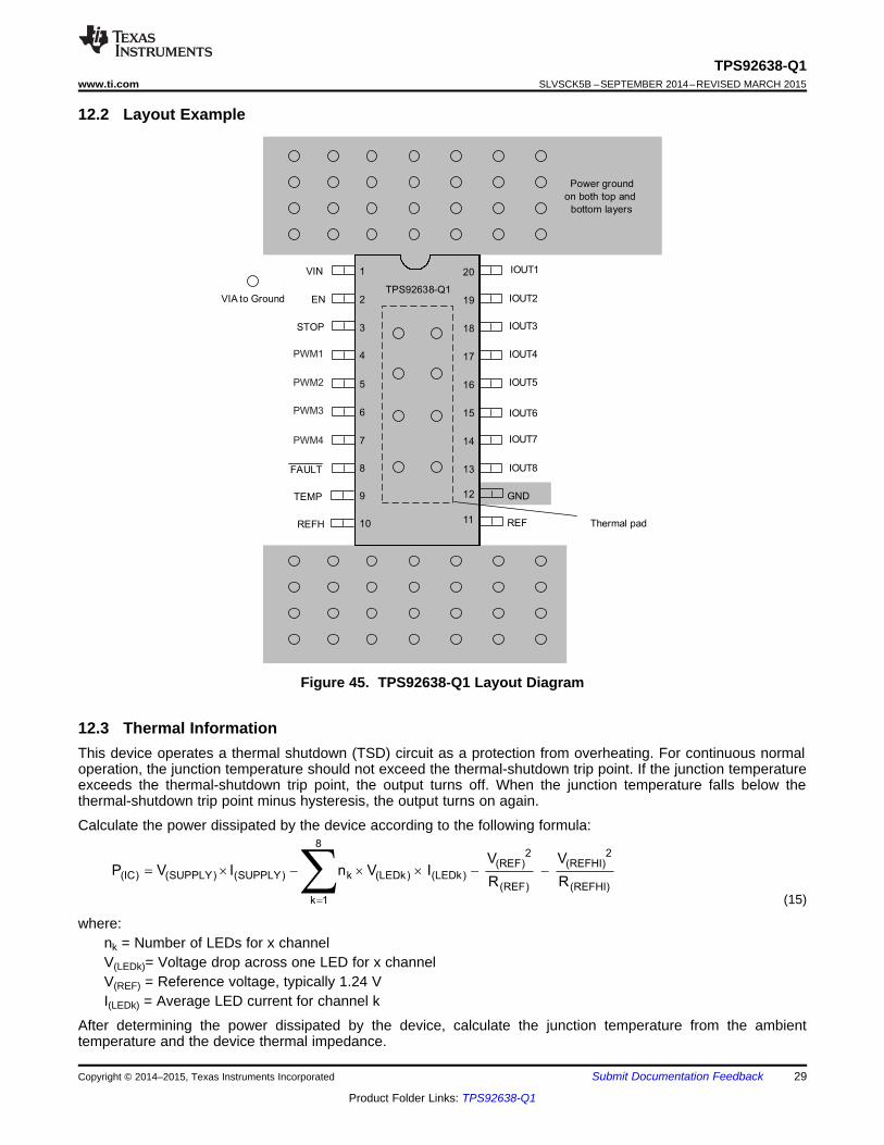
12.1 Layout GuidelinesIn order to prevent thermal shutdown, TJ must be less than 150°C. If the input voltage is very high, the powerdissipation might be large. Currently there is the TSSOP-EP package which has good thermal impedance, but atthe same time, the PCB layout is also very important. Good PCB design can optimize heat transfer, which isabsolutely essential for the long-term reliability of the device.• Maximize the copper coverage on the PCB to increase the thermal conductivity of the board, because the
major heat-flow path from the package to the ambient is through the copper on the PCB. Maximum copper isextremely important when there are not any heat sinks attached to the PCB on the other side of the package.
• Add as many thermal vias as possible directly under the package ground pad to optimize the thermalconductivity of the board.
• All thermal vias should be either plated shut or plugged and capped on both sides of the board to preventsolder voids. To ensure reliability and performance, the solder coverage should be at least 85%.
82 2
(REF) (REFHI)(IC) (SUPPLY) (SUPPLY) k (LEDk) (LEDk)
(REF) (REFHI)
k 1
V VP V I n V I
R R
=
= ´ - ´ ´ - -å
VIN
ENTPS92638-Q1
FAULT
STOP
GND
REF
TEMP
REFH
1
2
3
4
5
6
7
8
9
10
13
14
15
16
17
18
19
20
12
11
Power ground
on both top and
bottom layers
VIA to Ground
Thermal pad
IOUT1
IOUT2
IOUT3
IOUT4
IOUT5
IOUT6
IOUT7
IOUT8
PWM1
PWM2
PWM3
PWM4
29
TPS92638-Q1www.ti.com SLVSCK5B –SEPTEMBER 2014–REVISED MARCH 2015
Product Folder Links: TPS92638-Q1
Submit Documentation FeedbackCopyright © 2014–2015, Texas Instruments Incorporated
12.2 Layout Example
Figure 45. TPS92638-Q1 Layout Diagram
12.3 Thermal InformationThis device operates a thermal shutdown (TSD) circuit as a protection from overheating. For continuous normaloperation, the junction temperature should not exceed the thermal-shutdown trip point. If the junction temperatureexceeds the thermal-shutdown trip point, the output turns off. When the junction temperature falls below thethermal-shutdown trip point minus hysteresis, the output turns on again.
Calculate the power dissipated by the device according to the following formula:
(15)
where:nk = Number of LEDs for x channelV(LEDk)= Voltage drop across one LED for x channelV(REF) = Reference voltage, typically 1.24 VI(LEDk) = Average LED current for channel k
After determining the power dissipated by the device, calculate the junction temperature from the ambienttemperature and the device thermal impedance.
J A JA (IC)T T R Pq
= + ´
30
TPS92638-Q1SLVSCK5B –SEPTEMBER 2014–REVISED MARCH 2015 www.ti.com
Product Folder Links: TPS92638-Q1
Submit Documentation Feedback Copyright © 2014–2015, Texas Instruments Incorporated
Thermal Information (continued)
(16)
where:TA = Ambient temperatureRθJA = Junction-to-ambient thermal impedanceP(IC) = Dissipated power
31
TPS92638-Q1www.ti.com SLVSCK5B –SEPTEMBER 2014–REVISED MARCH 2015
Product Folder Links: TPS92638-Q1
Submit Documentation FeedbackCopyright © 2014–2015, Texas Instruments Incorporated
13 Device and Documentation Support
13.1 TrademarksAll trademarks are the property of their respective owners.
13.2 Electrostatic Discharge CautionThese devices have limited built-in ESD protection. The leads should be shorted together or the device placed in conductive foamduring storage or handling to prevent electrostatic damage to the MOS gates.
13.3 GlossarySLYZ022 — TI Glossary.
This glossary lists and explains terms, acronyms, and definitions.
14 Mechanical, Packaging, and Orderable InformationThe following pages include mechanical, packaging, and orderable information. This information is the most-current data available for the designated devices. This data is subject to change without notice and withoutrevision of this document. For browser-based versions of this data sheet, see the left-hand navigation pane.

PACKAGE OPTION ADDENDUM
www.ti.com 2-Apr-2015
Addendum-Page 1
PACKAGING INFORMATION
Orderable Device Status(1)
Package Type PackageDrawing
Pins PackageQty
Eco Plan(2)
Lead/Ball Finish(6)
MSL Peak Temp(3)
Op Temp (°C) Device Marking(4/5)
Samples
TPS92638QPWPRQ1 ACTIVE HTSSOP PWP 20 2000 Green (RoHS& no Sb/Br)
CU NIPDAU Level-3-260C-168 HR -40 to 125 TPS92638
(1) The marketing status values are defined as follows:ACTIVE: Product device recommended for new designs.LIFEBUY: TI has announced that the device will be discontinued, and a lifetime-buy period is in effect.NRND: Not recommended for new designs. Device is in production to support existing customers, but TI does not recommend using this part in a new design.PREVIEW: Device has been announced but is not in production. Samples may or may not be available.OBSOLETE: TI has discontinued the production of the device.
(2) Eco Plan - The planned eco-friendly classification: Pb-Free (RoHS), Pb-Free (RoHS Exempt), or Green (RoHS & no Sb/Br) - please check http://www.ti.com/productcontent for the latest availabilityinformation and additional product content details.TBD: The Pb-Free/Green conversion plan has not been defined.Pb-Free (RoHS): TI's terms "Lead-Free" or "Pb-Free" mean semiconductor products that are compatible with the current RoHS requirements for all 6 substances, including the requirement thatlead not exceed 0.1% by weight in homogeneous materials. Where designed to be soldered at high temperatures, TI Pb-Free products are suitable for use in specified lead-free processes.Pb-Free (RoHS Exempt): This component has a RoHS exemption for either 1) lead-based flip-chip solder bumps used between the die and package, or 2) lead-based die adhesive used betweenthe die and leadframe. The component is otherwise considered Pb-Free (RoHS compatible) as defined above.Green (RoHS & no Sb/Br): TI defines "Green" to mean Pb-Free (RoHS compatible), and free of Bromine (Br) and Antimony (Sb) based flame retardants (Br or Sb do not exceed 0.1% by weightin homogeneous material)
(3) MSL, Peak Temp. - The Moisture Sensitivity Level rating according to the JEDEC industry standard classifications, and peak solder temperature.
(4) There may be additional marking, which relates to the logo, the lot trace code information, or the environmental category on the device.
(5) Multiple Device Markings will be inside parentheses. Only one Device Marking contained in parentheses and separated by a "~" will appear on a device. If a line is indented then it is a continuationof the previous line and the two combined represent the entire Device Marking for that device.
(6) Lead/Ball Finish - Orderable Devices may have multiple material finish options. Finish options are separated by a vertical ruled line. Lead/Ball Finish values may wrap to two lines if the finishvalue exceeds the maximum column width.
Important Information and Disclaimer:The information provided on this page represents TI's knowledge and belief as of the date that it is provided. TI bases its knowledge and belief on informationprovided by third parties, and makes no representation or warranty as to the accuracy of such information. Efforts are underway to better integrate information from third parties. TI has taken andcontinues to take reasonable steps to provide representative and accurate information but may not have conducted destructive testing or chemical analysis on incoming materials and chemicals.TI and TI suppliers consider certain information to be proprietary, and thus CAS numbers and other limited information may not be available for release.
In no event shall TI's liability arising out of such information exceed the total purchase price of the TI part(s) at issue in this document sold by TI to Customer on an annual basis.
PACKAGE OPTION ADDENDUM
www.ti.com 2-Apr-2015
Addendum-Page 2
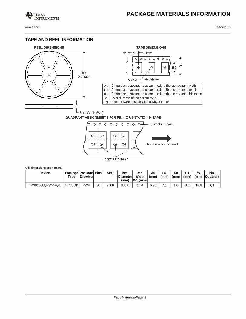
TAPE AND REEL INFORMATION
*All dimensions are nominal
Device PackageType
PackageDrawing
Pins SPQ ReelDiameter
(mm)
ReelWidth
W1 (mm)
A0(mm)
B0(mm)
K0(mm)
P1(mm)
W(mm)
Pin1Quadrant
TPS92638QPWPRQ1 HTSSOP PWP 20 2000 330.0 16.4 6.95 7.1 1.6 8.0 16.0 Q1
PACKAGE MATERIALS INFORMATION
www.ti.com 2-Apr-2015
Pack Materials-Page 1

*All dimensions are nominal
Device Package Type Package Drawing Pins SPQ Length (mm) Width (mm) Height (mm)
TPS92638QPWPRQ1 HTSSOP PWP 20 2000 367.0 367.0 38.0
PACKAGE MATERIALS INFORMATION
www.ti.com 2-Apr-2015
Pack Materials-Page 2
IMPORTANT NOTICE
Texas Instruments Incorporated (TI) reserves the right to make corrections, enhancements, improvements and other changes to itssemiconductor products and services per JESD46, latest issue, and to discontinue any product or service per JESD48, latest issue. Buyersshould obtain the latest relevant information before placing orders and should verify that such information is current and complete.TI’s published terms of sale for semiconductor products (http://www.ti.com/sc/docs/stdterms.htm) apply to the sale of packaged integratedcircuit products that TI has qualified and released to market. Additional terms may apply to the use or sale of other types of TI products andservices.Reproduction of significant portions of TI information in TI data sheets is permissible only if reproduction is without alteration and isaccompanied by all associated warranties, conditions, limitations, and notices. TI is not responsible or liable for such reproduceddocumentation. Information of third parties may be subject to additional restrictions. Resale of TI products or services with statementsdifferent from or beyond the parameters stated by TI for that product or service voids all express and any implied warranties for theassociated TI product or service and is an unfair and deceptive business practice. TI is not responsible or liable for any such statements.Buyers and others who are developing systems that incorporate TI products (collectively, “Designers”) understand and agree that Designersremain responsible for using their independent analysis, evaluation and judgment in designing their applications and that Designers havefull and exclusive responsibility to assure the safety of Designers' applications and compliance of their applications (and of all TI productsused in or for Designers’ applications) with all applicable regulations, laws and other applicable requirements. Designer represents that, withrespect to their applications, Designer has all the necessary expertise to create and implement safeguards that (1) anticipate dangerousconsequences of failures, (2) monitor failures and their consequences, and (3) lessen the likelihood of failures that might cause harm andtake appropriate actions. Designer agrees that prior to using or distributing any applications that include TI products, Designer willthoroughly test such applications and the functionality of such TI products as used in such applications.TI’s provision of technical, application or other design advice, quality characterization, reliability data or other services or information,including, but not limited to, reference designs and materials relating to evaluation modules, (collectively, “TI Resources”) are intended toassist designers who are developing applications that incorporate TI products; by downloading, accessing or using TI Resources in anyway, Designer (individually or, if Designer is acting on behalf of a company, Designer’s company) agrees to use any particular TI Resourcesolely for this purpose and subject to the terms of this Notice.TI’s provision of TI Resources does not expand or otherwise alter TI’s applicable published warranties or warranty disclaimers for TIproducts, and no additional obligations or liabilities arise from TI providing such TI Resources. TI reserves the right to make corrections,enhancements, improvements and other changes to its TI Resources. TI has not conducted any testing other than that specificallydescribed in the published documentation for a particular TI Resource.Designer is authorized to use, copy and modify any individual TI Resource only in connection with the development of applications thatinclude the TI product(s) identified in such TI Resource. NO OTHER LICENSE, EXPRESS OR IMPLIED, BY ESTOPPEL OR OTHERWISETO ANY OTHER TI INTELLECTUAL PROPERTY RIGHT, AND NO LICENSE TO ANY TECHNOLOGY OR INTELLECTUAL PROPERTYRIGHT OF TI OR ANY THIRD PARTY IS GRANTED HEREIN, including but not limited to any patent right, copyright, mask work right, orother intellectual property right relating to any combination, machine, or process in which TI products or services are used. Informationregarding or referencing third-party products or services does not constitute a license to use such products or services, or a warranty orendorsement thereof. Use of TI Resources may require a license from a third party under the patents or other intellectual property of thethird party, or a license from TI under the patents or other intellectual property of TI.TI RESOURCES ARE PROVIDED “AS IS” AND WITH ALL FAULTS. TI DISCLAIMS ALL OTHER WARRANTIES ORREPRESENTATIONS, EXPRESS OR IMPLIED, REGARDING RESOURCES OR USE THEREOF, INCLUDING BUT NOT LIMITED TOACCURACY OR COMPLETENESS, TITLE, ANY EPIDEMIC FAILURE WARRANTY AND ANY IMPLIED WARRANTIES OFMERCHANTABILITY, FITNESS FOR A PARTICULAR PURPOSE, AND NON-INFRINGEMENT OF ANY THIRD PARTY INTELLECTUALPROPERTY RIGHTS. TI SHALL NOT BE LIABLE FOR AND SHALL NOT DEFEND OR INDEMNIFY DESIGNER AGAINST ANY CLAIM,INCLUDING BUT NOT LIMITED TO ANY INFRINGEMENT CLAIM THAT RELATES TO OR IS BASED ON ANY COMBINATION OFPRODUCTS EVEN IF DESCRIBED IN TI RESOURCES OR OTHERWISE. IN NO EVENT SHALL TI BE LIABLE FOR ANY ACTUAL,DIRECT, SPECIAL, COLLATERAL, INDIRECT, PUNITIVE, INCIDENTAL, CONSEQUENTIAL OR EXEMPLARY DAMAGES INCONNECTION WITH OR ARISING OUT OF TI RESOURCES OR USE THEREOF, AND REGARDLESS OF WHETHER TI HAS BEENADVISED OF THE POSSIBILITY OF SUCH DAMAGES.Unless TI has explicitly designated an individual product as meeting the requirements of a particular industry standard (e.g., ISO/TS 16949and ISO 26262), TI is not responsible for any failure to meet such industry standard requirements.Where TI specifically promotes products as facilitating functional safety or as compliant with industry functional safety standards, suchproducts are intended to help enable customers to design and create their own applications that meet applicable functional safety standardsand requirements. Using products in an application does not by itself establish any safety features in the application. Designers mustensure compliance with safety-related requirements and standards applicable to their applications. Designer may not use any TI products inlife-critical medical equipment unless authorized officers of the parties have executed a special contract specifically governing such use.Life-critical medical equipment is medical equipment where failure of such equipment would cause serious bodily injury or death (e.g., lifesupport, pacemakers, defibrillators, heart pumps, neurostimulators, and implantables). Such equipment includes, without limitation, allmedical devices identified by the U.S. Food and Drug Administration as Class III devices and equivalent classifications outside the U.S.TI may expressly designate certain products as completing a particular qualification (e.g., Q100, Military Grade, or Enhanced Product).Designers agree that it has the necessary expertise to select the product with the appropriate qualification designation for their applicationsand that proper product selection is at Designers’ own risk. Designers are solely responsible for compliance with all legal and regulatoryrequirements in connection with such selection.Designer will fully indemnify TI and its representatives against any damages, costs, losses, and/or liabilities arising out of Designer’s non-compliance with the terms and provisions of this Notice.
Mailing Address: Texas Instruments, Post Office Box 655303, Dallas, Texas 75265Copyright © 2017, Texas Instruments Incorporated