Embed Size (px)
Citation preview
Transistor Technologies
for High Efficiency and Linearity

HEMT
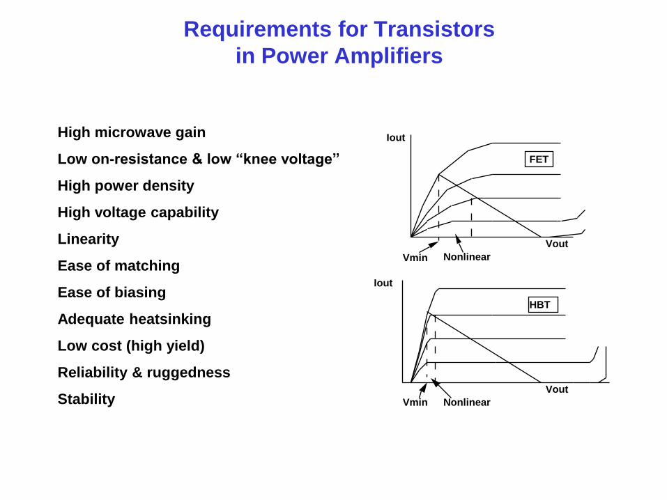
Requirements for Transistors
in Power Amplifiers
Iout
Vout
Vmin Nonlinear
FET
Iout
Vout
Vmin Nonlinear
HBT
High microwave gain
Low on-resistance & low “knee voltage”
High power density
High voltage capability
Linearity
Ease of matching
Ease of biasing
Adequate heatsinking
Low cost (high yield)
Reliability & ruggedness
Stability

Central Concern for Transistors in ECE265C
What is highest voltage that can be maintained?
What is highest current that can be delivered?
What is highest power that can be withstood?
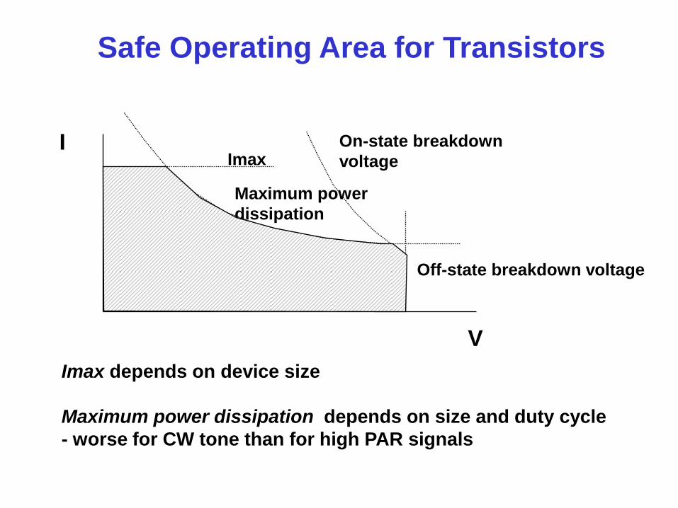
Safe Operating Area for Transistors
I
V
Imax On-state breakdown
voltage
Off-state breakdown voltage
Maximum power
dissipation
Imax depends on device size
Maximum power dissipation depends on size and duty cycle
- worse for CW tone than for high PAR signals

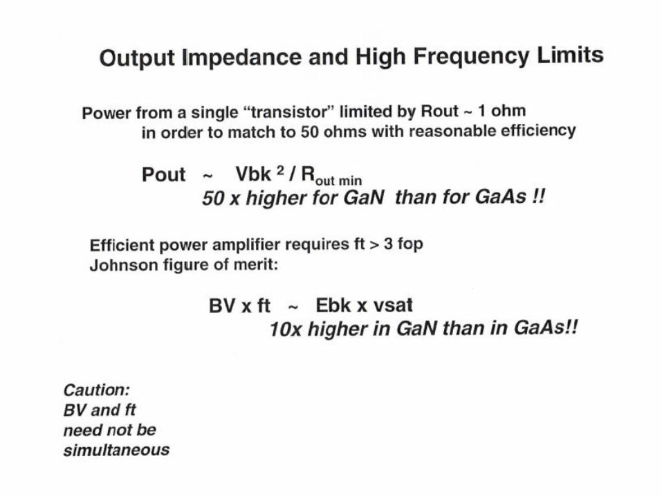
Tradeoff of Breakdown Voltage and ft
To avoid breakdown, generally must limit peak electric field to below
a critical value, Eb
To achieve high voltage, one can design the high field region to be
long:
Vbk= Eb *wc
The large wc tends to increase transit time for carriers,
resulting in low ft:
Ttr>wc/vsat, Ft=1/(2p Ttr)
The product of Vbk and ft tends to be independent of wc:
Vbk*ft <= Eb * vsat / 2 p
CMOS scaling through Moore’s Law acts to drive up ft, but it
drives down Vbk at the same time.
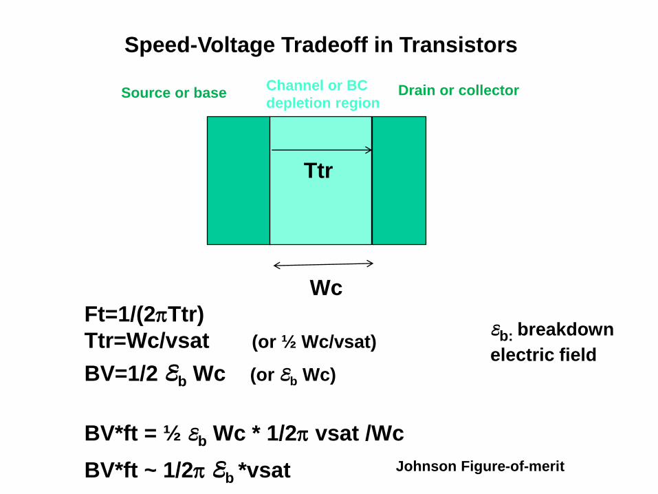
Ft=1/(2pTtr)
Ttr=Wc/vsat (or ½ Wc/vsat)
BV=1/2 Eb Wc (or Eb Wc)
BV*ft = ½ Eb Wc * 1/2p vsat /Wc
BV*ft ~ 1/2p Eb *vsat
Speed-Voltage Tradeoff in Transistors
Channel or BC
depletion region Drain or collector Source or base
Wc
Ttr
Johnson Figure-of-merit
Eb: breakdown
electric field
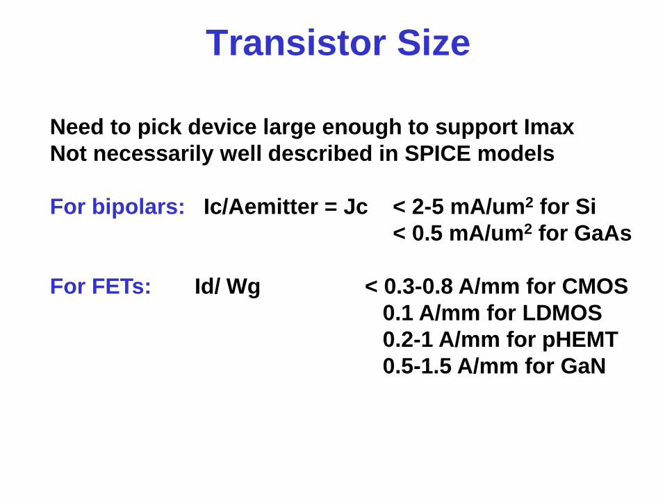
Transistor Size
Need to pick device large enough to support Imax
Not necessarily well described in SPICE models
For bipolars: Ic/Aemitter = Jc < 2-5 mA/um2 for Si
< 0.5 mA/um2 for GaAs
For FETs: Id/ Wg < 0.3-0.8 A/mm for CMOS
0.1 A/mm for LDMOS
0.2-1 A/mm for pHEMT
0.5-1.5 A/mm for GaN

Thermal Effects in Power Transistors
•Burnout (melting of portions of device, rapid diffusion of
defects, excess stress, etc)
•Degradation
•Thermal runaway in bipolar transistors
•Decreased performance: reduced Iout, lower ft, etc
•Thermally induced distortion & memory effect
•Difference between cw and short-time ac characteristics
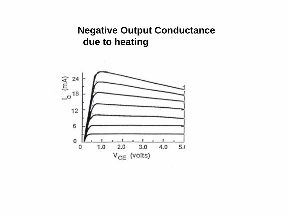
Negative Output Conductance
due to heating

Basics of Thermal Circuits
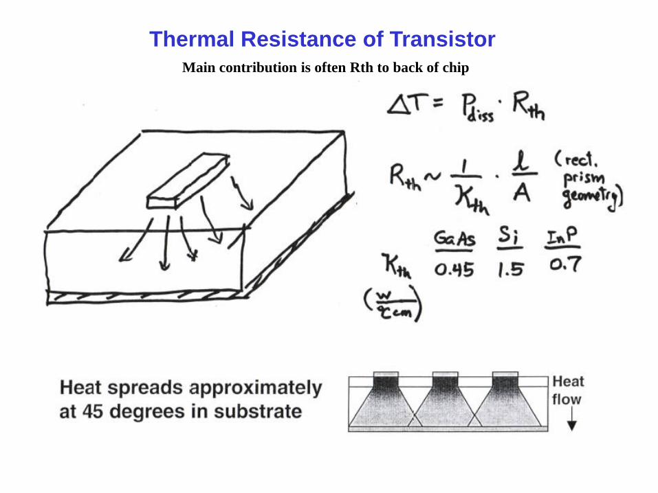
Thermal Resistance of Transistor Main contribution is often Rth to back of chip
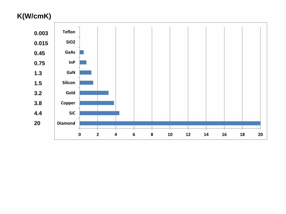
0 2 4 6 8 10 12 14 16 18 20
Diamond
SiC
Copper
Gold
Silicon
GaN
InP
GaAs
SiO2
Teflon
K(W/cmK)
0.003
0.015
0.45
0.75
1.3
1.5
3.2
3.8
4.4
20

Thermal Resistance Calculations Using
3D Structure Simulators
(solve Laplace’s equation)
Ansys, comsol, sentaurus, etc
InP HBT CMOS SOI

Thermal Resistance Estimate 1
Rth for section near
device is >> Rth at bottom
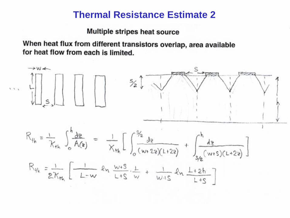
Thermal Resistance Estimate 2

How To Decrease Thermal Resistance
Thin substrates
Thermal Vias
Heat Spreaders
Flip-chip bonding (? sometimes)
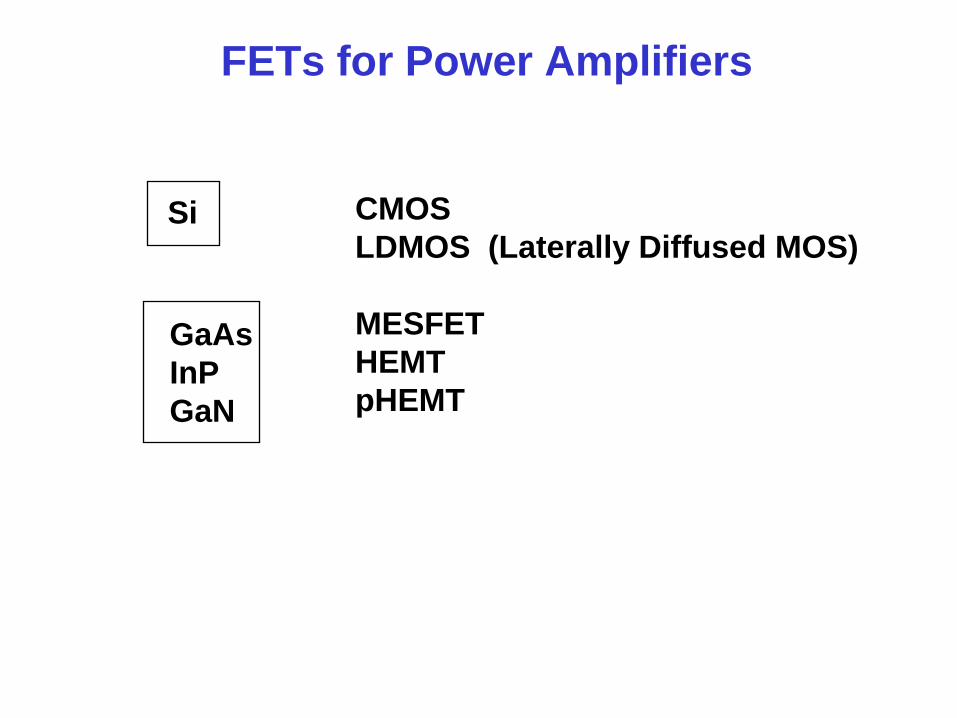
FETs for Power Amplifiers
CMOS
LDMOS (Laterally Diffused MOS)
MESFET
HEMT
pHEMT
Si
GaAs
InP
GaN
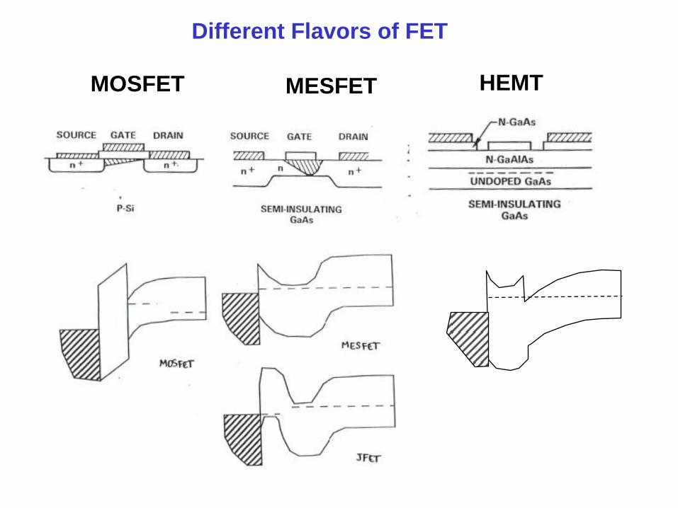
Different Flavors of FET
MOSFET MESFET HEMT
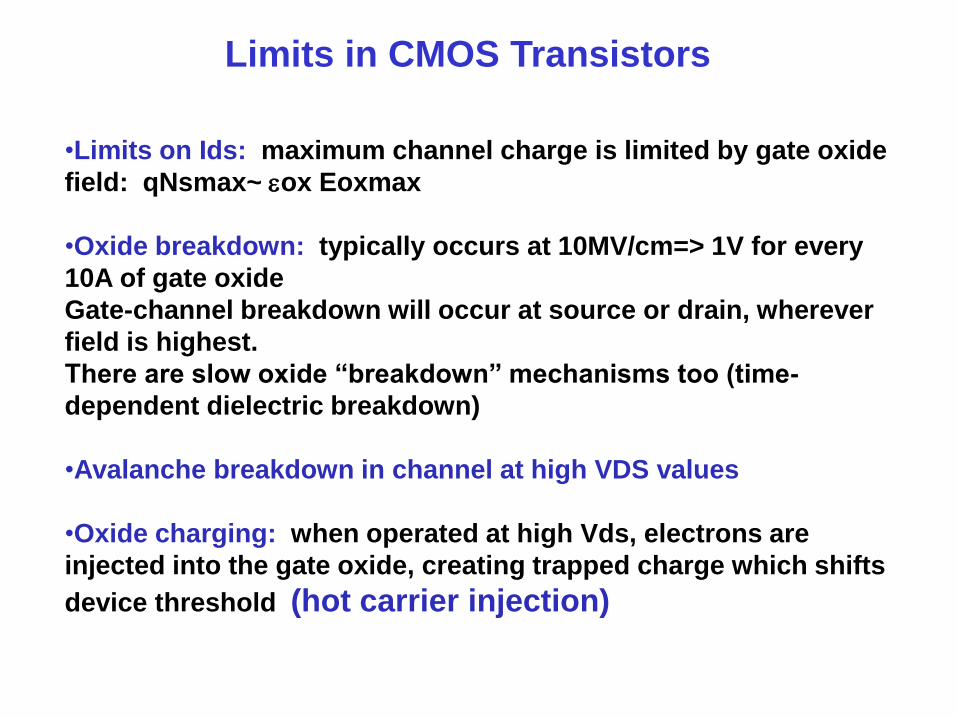
Limits in CMOS Transistors
•Limits on Ids: maximum channel charge is limited by gate oxide
field: qNsmax~ eox Eoxmax
•Oxide breakdown: typically occurs at 10MV/cm=> 1V for every
10A of gate oxide
Gate-channel breakdown will occur at source or drain, wherever
field is highest.
There are slow oxide “breakdown” mechanisms too (time-
dependent dielectric breakdown)
•Avalanche breakdown in channel at high VDS values
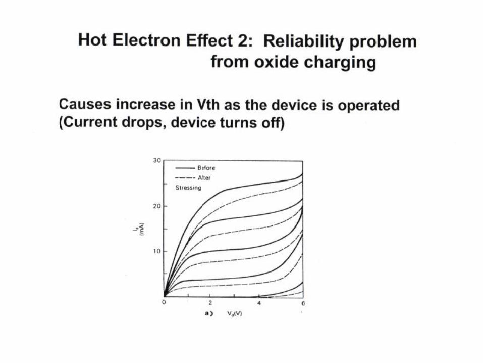
•Oxide charging: when operated at high Vds, electrons are
injected into the gate oxide, creating trapped charge which shifts
device threshold (hot carrier injection)
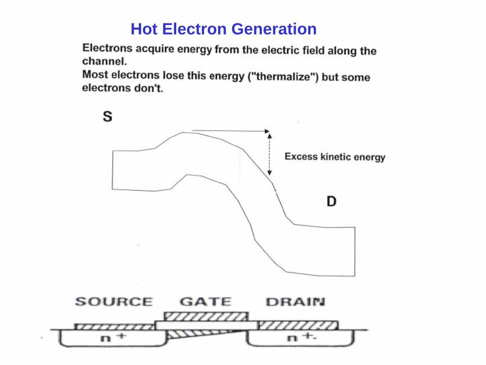
Hot Electron Generation

Source Channel Drain
High electric field
- - + -
High Voltage Breakdown Mechanism of MOS Transistor
Impact ionization at drain edge of gate
What happens to holes generated by impact ionization?
They flow to the substrate and to the source.
They cause some extra current due to body effect.
They can be measured as substrate or well current.
Moderate electric field


0.5 1.0 1.5 2.0 2.50.0 3.0
0.5
1.0
1.5
2.0
0.0
2.5
Vds
ID.i, A
CMOS Id-Vds curve
(generic)
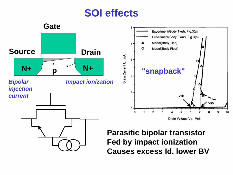
SOI effects
Gate
Source Drain
Impact ionization Bipolar
injection
current
N+ N+ p
Parasitic bipolar transistor
Fed by impact ionization
Causes excess Id, lower BV
"snapback"
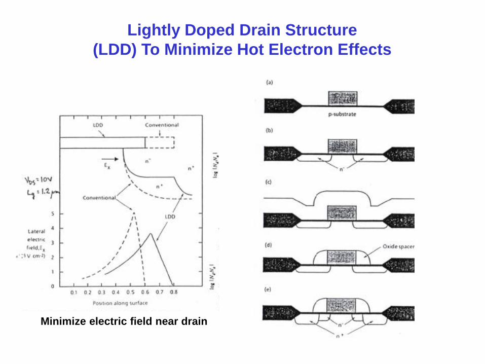
Lightly Doped Drain Structure
(LDD) To Minimize Hot Electron Effects
Minimize electric field near drain

Differential Topology
• Double the available voltage swing
• Even-order harmonic suppression
• Double the frequency of current injection into substrate
– Reduce the potential for LO-pulling
• The tail current source is removed from the standard
differential pair (this is a “quasi-differential” structure)
– DC current set by the biasing of input devices
– Max. current set by the input voltage swing
• May require differential to single-ended output conversion
(balun)
Technique to improve CMOS PAs:
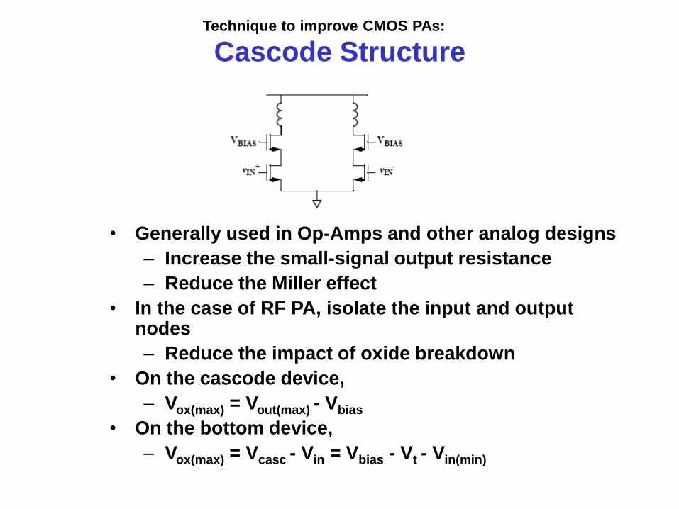
Cascode Structure
• Generally used in Op-Amps and other analog designs
– Increase the small-signal output resistance
– Reduce the Miller effect
• In the case of RF PA, isolate the input and output nodes
– Reduce the impact of oxide breakdown
• On the cascode device,
– Vox(max) = Vout(max) - Vbias
• On the bottom device,
– Vox(max) = Vcasc - Vin = Vbias - Vt - Vin(min)
Technique to improve CMOS PAs:

Id-Vds Characteristics of Cascode
vdd1
0V 0.5V 1.0V 1.5V 2.0V 2.5V
ID(m2) ID(m4)
0A
100mA
200mA
300mA
Id-Vds for Cascode:
Higher Ron
Lower Idmax
Body effect on top FET
Higher Vmin decreases
efficiency

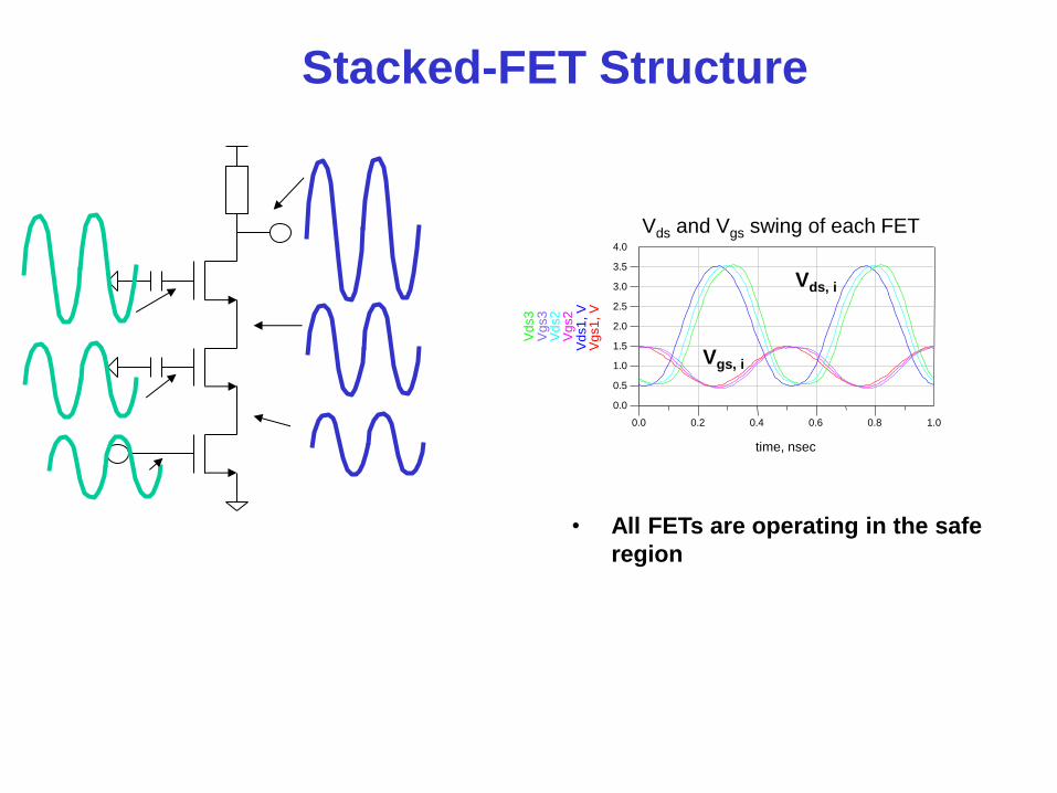
Stacked-FET Structure
0.2 0.4 0.6 0.8 0.0 1.0
0.5
1.0
1.5
2.0
2.5
3.0
3.5
0.0
4.0
time, nsec
Vg
s1
, V
V
ds1
, V
V
gs2
V
ds2
V
gs3
V
ds3
Vds, i
Vgs, i
Vds and Vgs swing of each FET
• All FETs are operating in the safe
region
Stacked-FET Structure
0.2 0.4 0.6 0.8 0.0 1.0
0.5
1.0
1.5
2.0
2.5
3.0
3.5
0.0
4.0
time, nsec
Vg
s1
, V
V
ds1
, V
V
gs2
V
ds2
V
gs3
V
ds3
Vds, i
Vgs, i
Vds and Vgs swing of each FET
• All FETs are operating in the safe
region

Stacked-FET Structure
C2
Zs2= Ropt
Zs3= 2Ropt
3Ropt
C3
m g C
gs C
s Z
1
2
1 2
+ @
Zs2
2
Tailor swing at each drain
and gate by proper
selection of gate capacitor
Id~gm Vgs
~gm Vt C2/(C2+Cgs)

Stacked FET Approach for CMOS PAs
-20
-15
-10
-5
0
5
10
75 80 85 90 95 100 105 110
S -
pa
ram
ete
rs (
dB
)
Freq (GHz)
50 mW Psat at 90GHz
In 45 nm CMOS SOI
Works well at least up to 90GHz !!!
Jefy Jayamon (UCSD)
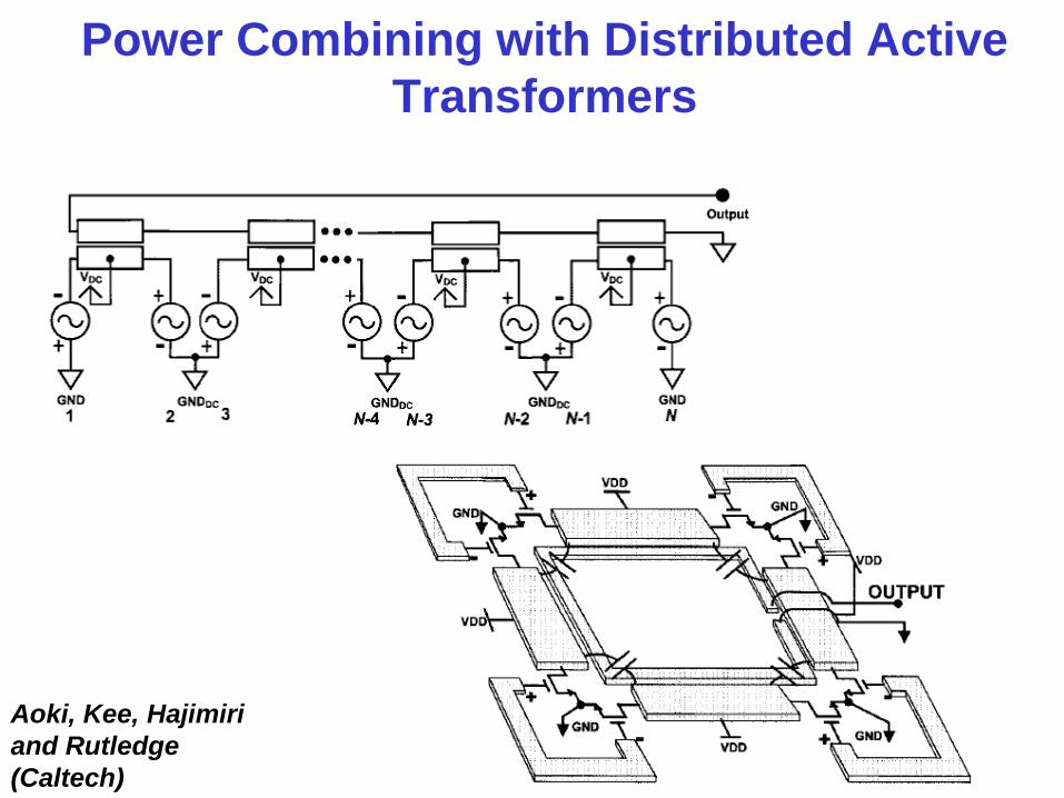
Power Combining with Distributed Active
Transformers
Aoki, Kee, Hajimiri
and Rutledge
(Caltech)
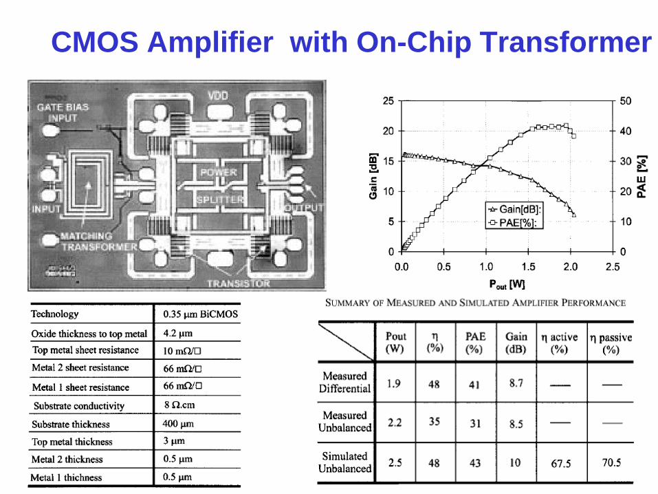
CMOS Amplifier with On-Chip Transformer

Grain of salt


LDMOS
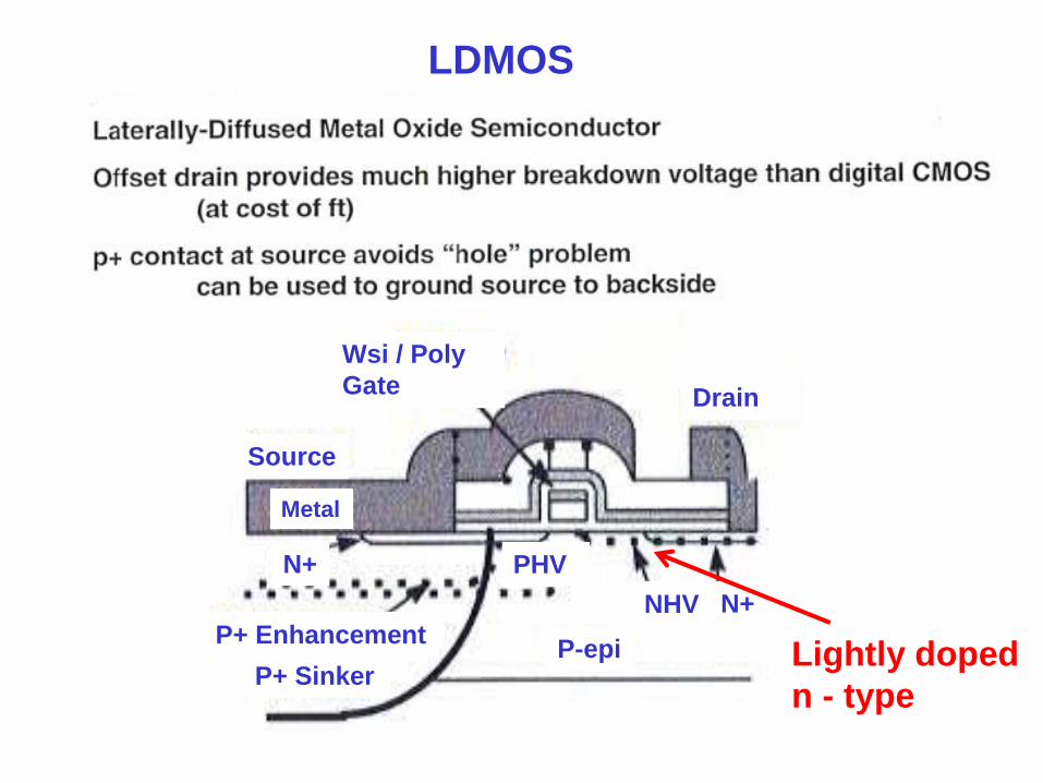
Drain
Wsi / Poly
Gate
Source
P+ Sinker P-epi
P+ Enhancement
NHV N+
N+ PHV
Metal
LDMOS
Lightly doped
n - type
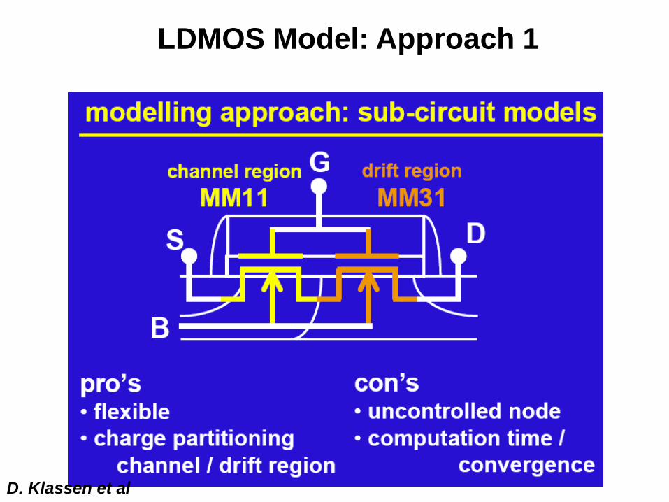
LDMOS Model: Approach 1
D. Klassen et al

LDMOS Transistors are current workhorses
for Basestation PAs
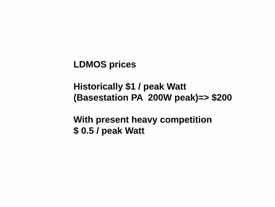
LDMOS prices
Historically $1 / peak Watt
(Basestation PA 200W peak)=> $200
With present heavy competition
$ 0.5 / peak Watt
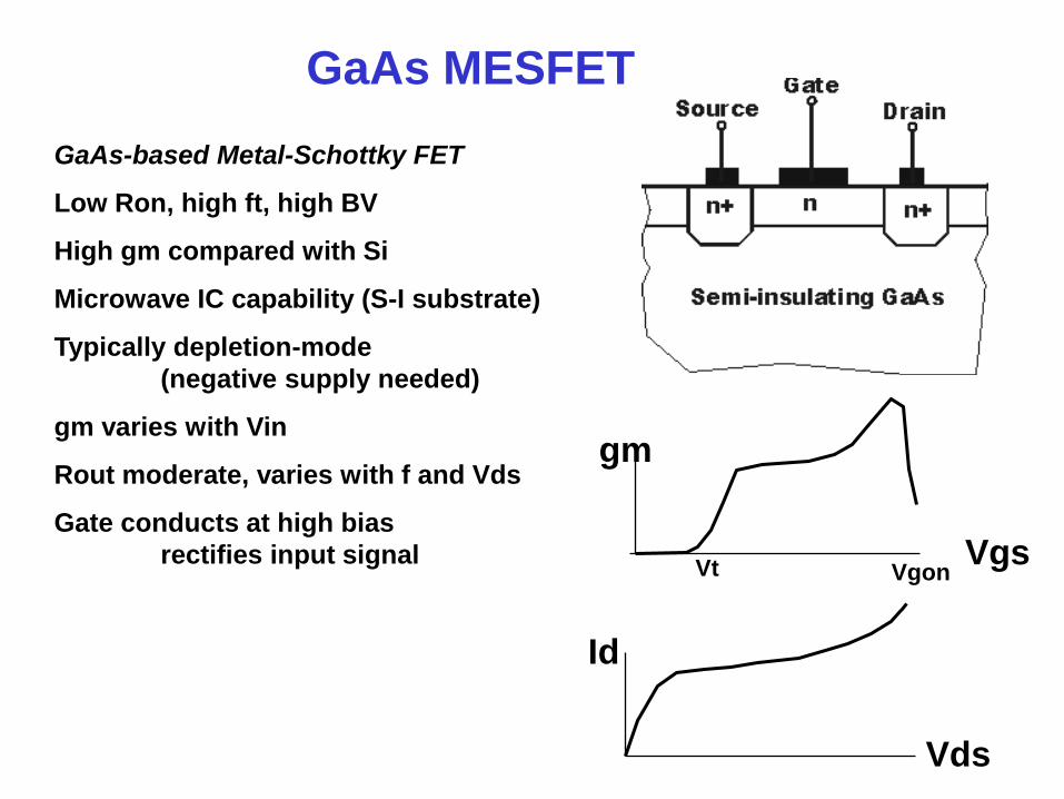
GaAs MESFET
GaAs-based Metal-Schottky FET
Low Ron, high ft, high BV
High gm compared with Si
Microwave IC capability (S-I substrate)
Typically depletion-mode
(negative supply needed)
gm varies with Vin
Rout moderate, varies with f and Vds
Gate conducts at high bias
rectifies input signal Vgs
gm
Vds
Id
Vt Vgon

Channel Charge in GaAs MESFETs
If reverse bias on Schottky gate is increased,
Channel becomes more depleted, channel charge decreases
Channel charge Q ~ q Nd (a-w) w=sqrt[2e(V+Vbi)/qNd]
X=w
Vgs
=> I-V curves similar to MOSFET
Gradual Channel Approx.
Id=1/2 CinmW/L(Vgs-Vt)2
in saturation region
Typically depletion mode
Q
Vt Vbi

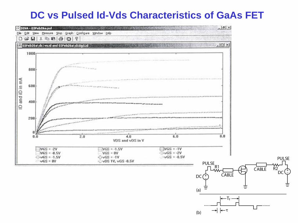
DC vs Pulsed Id-Vds Characteristics of GaAs FET
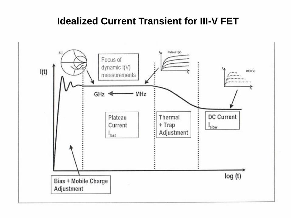
Idealized Current Transient for III-V FET
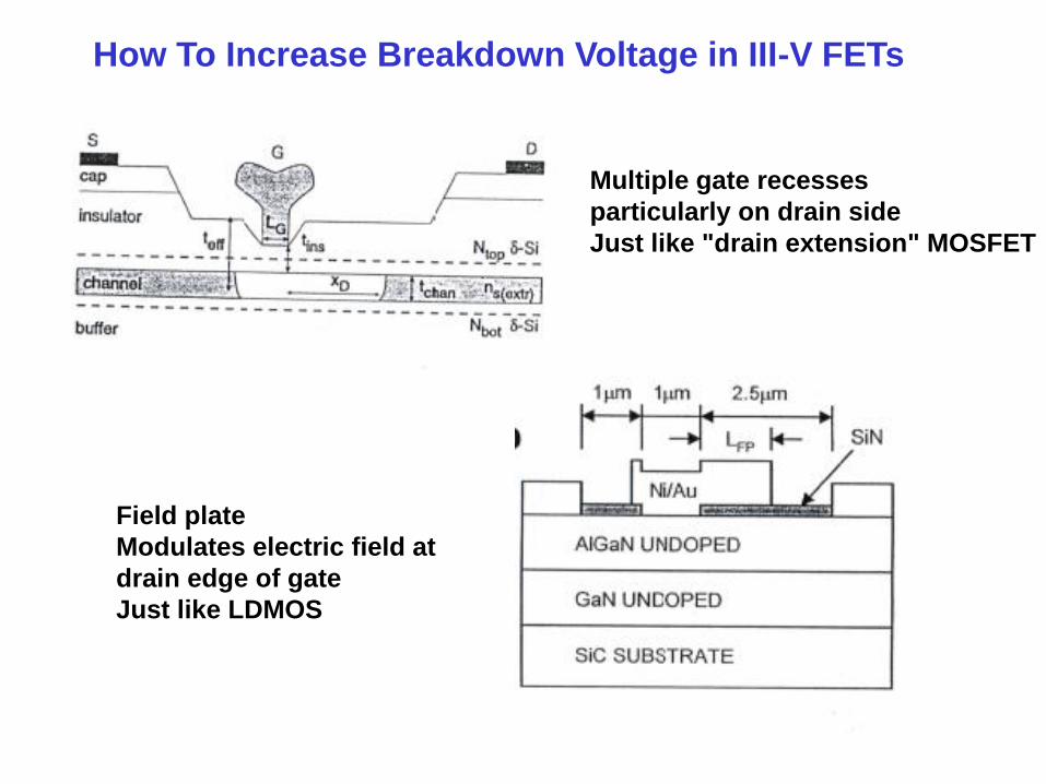
How To Increase Breakdown Voltage in III-V FETs
Multiple gate recesses
particularly on drain side
Just like "drain extension" MOSFET
Field plate
Modulates electric field at
drain edge of gate
Just like LDMOS
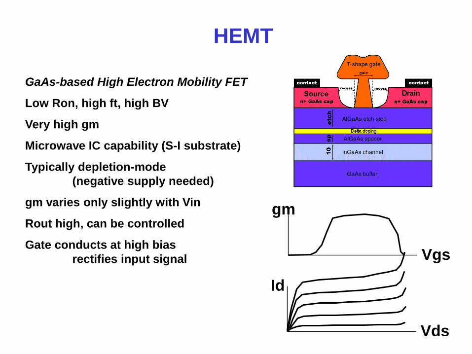
HEMT
GaAs-based High Electron Mobility FET
Low Ron, high ft, high BV
Very high gm
Microwave IC capability (S-I substrate)
Typically depletion-mode
(negative supply needed)
gm varies only slightly with Vin
Rout high, can be controlled
Gate conducts at high bias
rectifies input signal Vgs
gm
Vds
Id

HEMT MOSFET
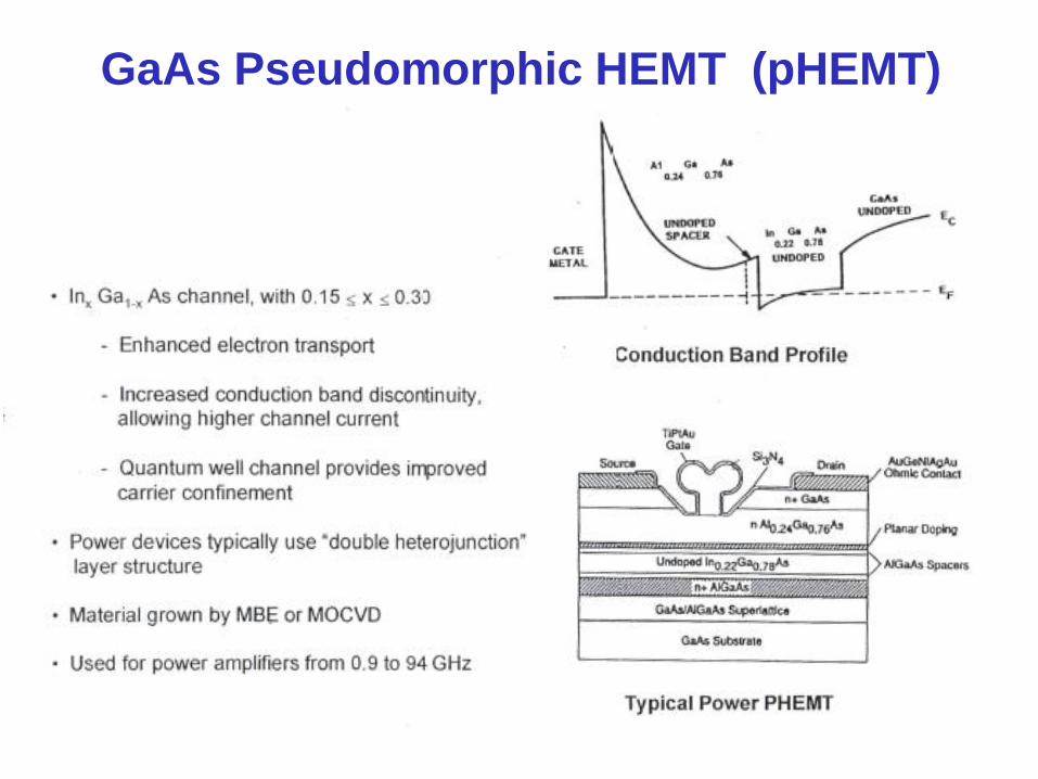
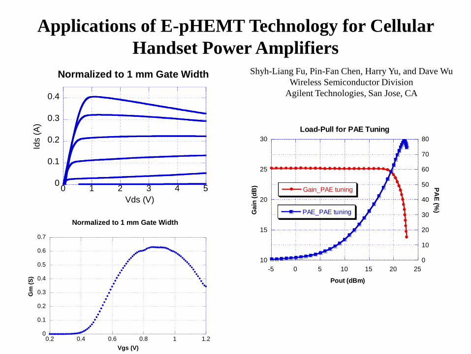
GaAs Pseudomorphic HEMT (pHEMT)
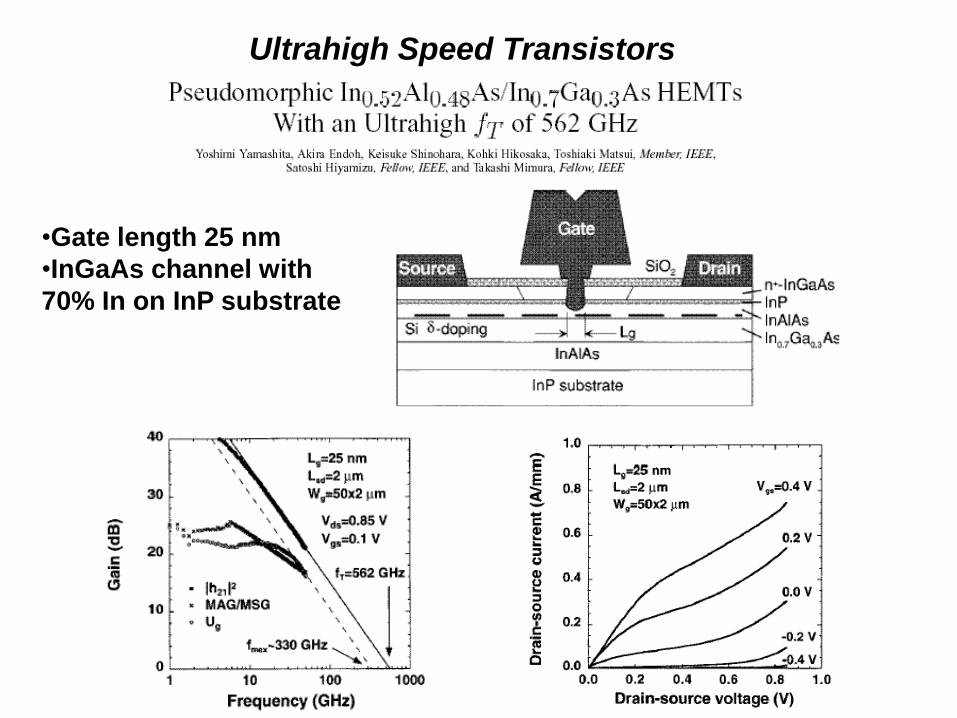
Ultrahigh Speed Transistors
•Gate length 25 nm
•InGaAs channel with
70% In on InP substrate
0
0.1
0.2
0.3
0.4
0 1 2 3 4 5
Normalized to 1 mm Gate Width
Ids (
A)
Vds (V)
10
15
20
25
30
0
10
20
30
40
50
60
70
80
-5 0 5 10 15 20 25
Load-Pull for PAE Tuning
Gain_PAE tuning
PAE_PAE tuningGa
in (
dB
) PA
E (%
)
Pout (dBm)
0
0.1
0.2
0.3
0.4
0.5
0.6
0.7
0.2 0.4 0.6 0.8 1 1.2
Normalized to 1 mm Gate Width
Gm
(S
)
Vgs (V)
Applications of E-pHEMT Technology for Cellular
Handset Power Amplifiers
Shyh-Liang Fu, Pin-Fan Chen, Harry Yu, and Dave Wu
Wireless Semiconductor Division
Agilent Technologies, San Jose, CA
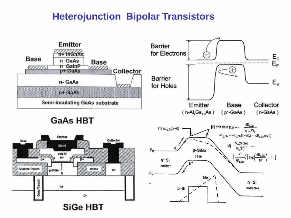
Heterojunction Bipolar Transistors

HBT
High microwave gain
High power density =small die size
Straightforward fabrication
(simple lithography
no Vth control problems)
Single power supply
High efficiency
Good linearity
Thermal issues
(including thermal runaway)
Pros
Cons Finite base current
Saturation charge storage
Heterojunction Bipolar Transistor

GaAs HBT Power Amplifier Example
WCDMA

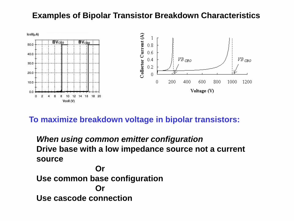
To maximize breakdown voltage in bipolar transistors:
When using common emitter configuration
Drive base with a low impedance source not a current
source
Or
Use common base configuration
Or
Use cascode connection
Examples of Bipolar Transistor Breakdown Characteristics
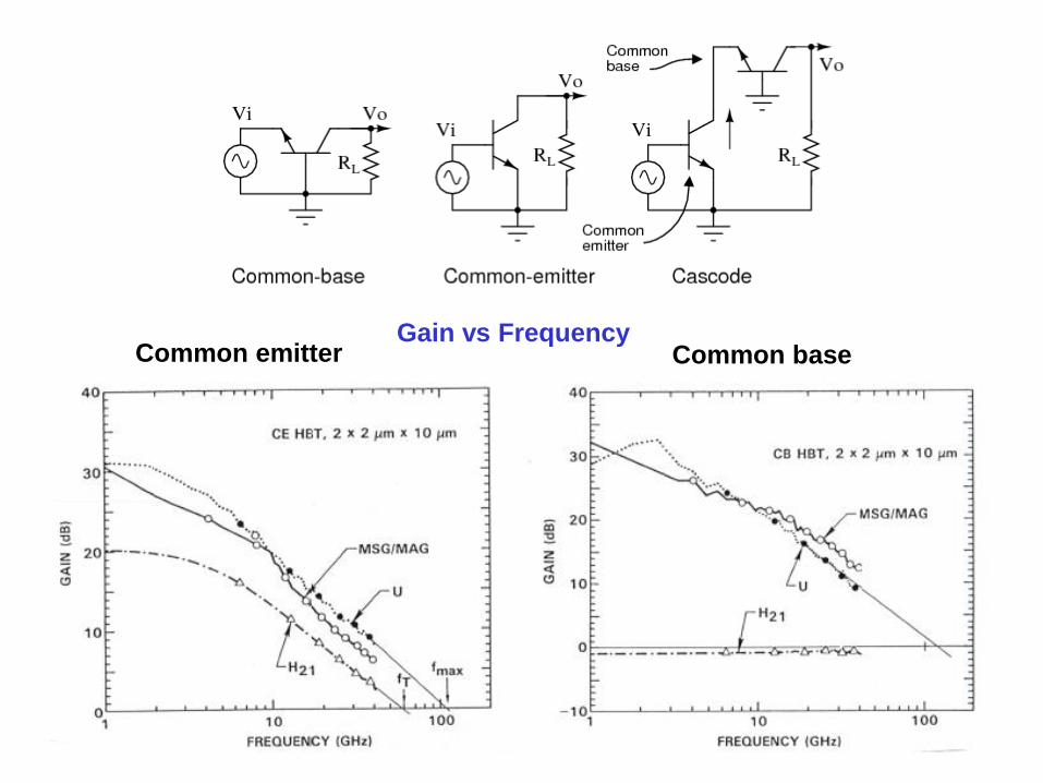
Gain vs Frequency Common emitter Common base

Bias Circuit Considerations
Do not want to short out RF input signal
Want temperature independent bias
Often use current mirror
Use smaller device to set bias, to conserve power
Basic circuits:
Vbias
Vbatt or Vref (can be BG reference)
Vbias
Vbatt or Vref
Qhelper supplies
current to feed bases
Rf in Rf in
This provides low
impedance near dc This provides low
impedance at rf

Thermal Runaway in BJTs and HBTs
At high Vce, dc behavior of Ic vs Vbe
shows increasing gm, then infinite gm,
then negative gm
=> Multivalued Ic
current splits between hot and
cold fingers
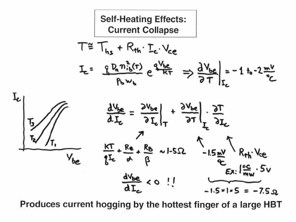

Bipolar Ic-Vce Curves with Thermal Runaway
Ic
Vce
Ib steps
Ic
Vce
Ib steps
HBT BJT
(no heterojunction)

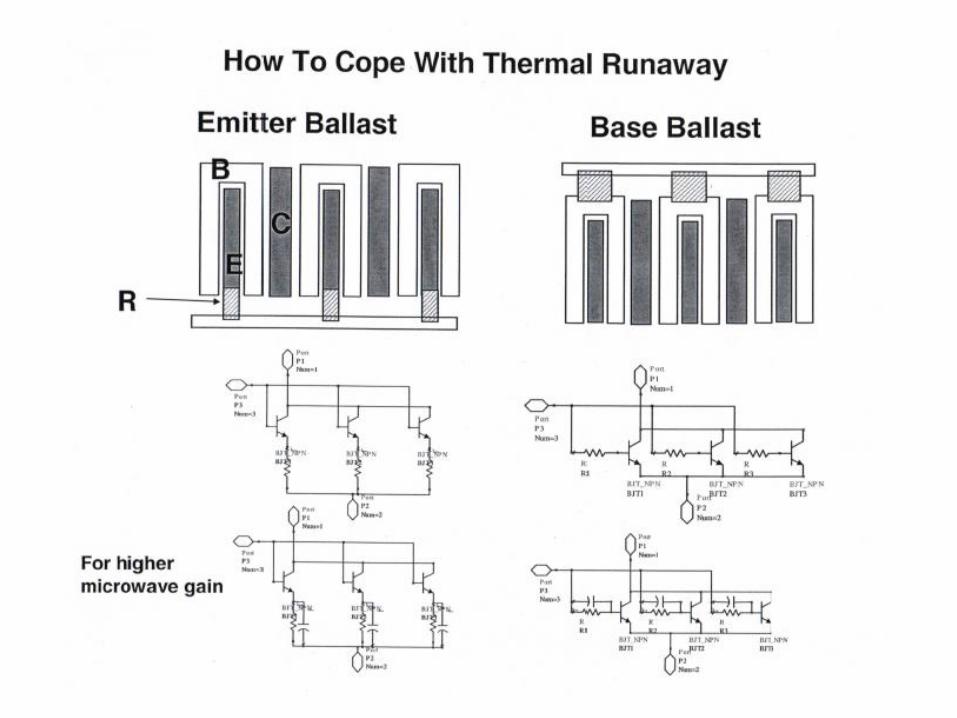
Include extra resistances in emitter fingers (ballast resistors) to
keep gm finite
Costs in gain and efficiency
Can put ballast resistors in base input (use value Reballast*beta)
In principle ballast resistors can be shorted by capacitors to
avoid drop in gain (but capacitors have to be very big and
numerous)
Solution to thermal runaway
Add extra Rb till >
Vbias
Vbatt or Vref
Rf in
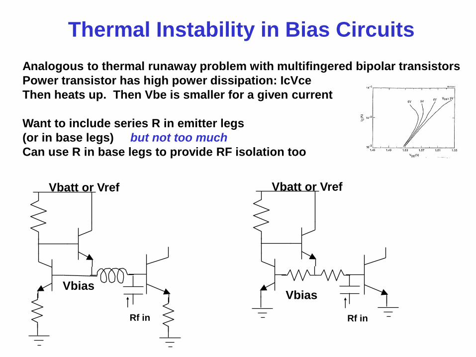
Thermal Instability in Bias Circuits
Analogous to thermal runaway problem with multifingered bipolar transistors
Power transistor has high power dissipation: IcVce
Then heats up. Then Vbe is smaller for a given current
Want to include series R in emitter legs
(or in base legs) but not too much
Can use R in base legs to provide RF isolation too
Vbias
Vbatt or Vref
Rf in
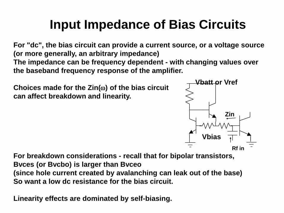
Input Impedance of Bias Circuits
For "dc", the bias circuit can provide a current source, or a voltage source
(or more generally, an arbitrary impedance)
The impedance can be frequency dependent - with changing values over
the baseband frequency response of the amplifier.
Choices made for the Zin(w) of the bias circuit
can affect breakdown and linearity.
For breakdown considerations - recall that for bipolar transistors,
Bvces (or Bvcbo) is larger than Bvceo
(since hole current created by avalanching can leak out of the base)
So want a low dc resistance for the bias circuit.
Linearity effects are dominated by self-biasing.
Vbias
Vbatt or Vref
Rf in
Zin
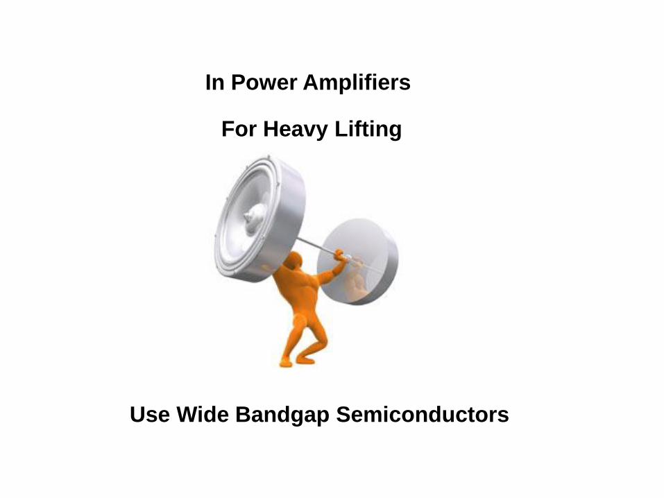
Use Wide Bandgap Semiconductors
In Power Amplifiers
For Heavy Lifting

0 5 10 15
Thermal conductivity (W cm/K)
Si
GaAs
InP
SiC 4H
GaN
sapphire
diamond
0 1 2 3 4
Breakdown Electric Field (MV/cm)
Si
GaAs
InP
SiC 4H
GaN
Wide Bandgap Material Properties

Electron Transport Characteristics
Mobility
(FET channels - cm2/Vs)
GaAs FET 4500
GaAs PHEMT 6000
InP HEMT 10000
Si 500
SiC 4H 400
GaN HFET 1500

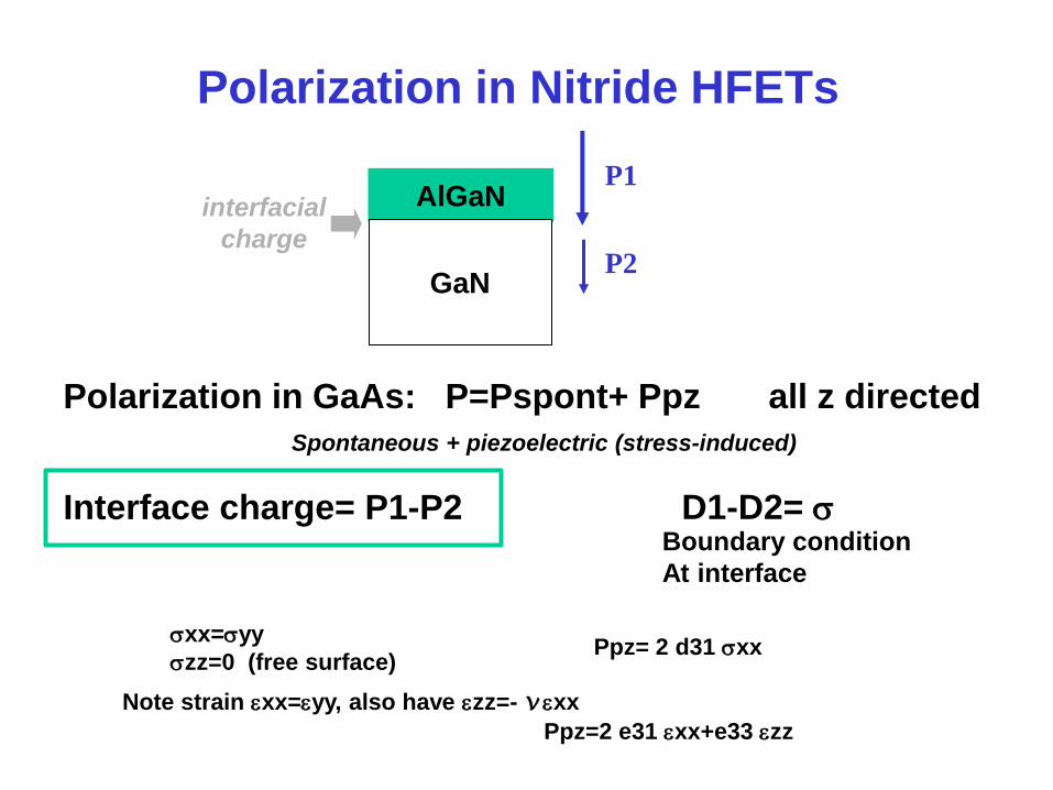
Polarization in Nitride HFETs
AlGaN
GaN
interfacial
charge P2
P1
Polarization in GaAs: P=Pspont+ Ppz all z directed
Ppz= 2 d31 sxx sxx=syy
szz=0 (free surface)
Interface charge= P1-P2
Note strain exx=eyy, also have ezz=- v exx
Ppz=2 e31 exx+e33 ezz
Spontaneous + piezoelectric (stress-induced)
D1-D2= s Boundary condition
At interface

2 DEG
GaN AlGaN
s sp
+ s pz
ssurf states
s2DEG
s sp
+ s pz
2 DEG
GaN AlGaN
s sp
+ s pz
smetal
s2DEG
s sp
+ s pz
S D
Field plate LFP
TSiNx
AlGaN/GaN HFET
structure GaN
AlGaN
SiC substrate