Embed Size (px)
Citation preview

This is an electronic reprint of the original article.This reprint may differ from the original in pagination and typographic detail.
Powered by TCPDF (www.tcpdf.org)
This material is protected by copyright and other intellectual property rights, and duplication or sale of all or part of any of the repository collections is not permitted, except that material may be duplicated by you for your research use or educational purposes in electronic or print form. You must obtain permission for any other use. Electronic or print copies may not be offered, whether for sale or otherwise to anyone who is not an authorised user.
Tuomisto, Noora; Zugarramurdi Camino, Asier; Puska, Martti J.Modeling of electron tunneling through a tilted potential barrier
Published in:Journal of Applied Physics
DOI:10.1063/1.4979533
Published: 07/04/2017
Document VersionPublisher's PDF, also known as Version of record
Please cite the original version:Tuomisto, N., Zugarramurdi Camino, A., & Puska, M. J. (2017). Modeling of electron tunneling through a tiltedpotential barrier. Journal of Applied Physics, 121(13), 1-10. [134304]. https://doi.org/10.1063/1.4979533

Modeling of electron tunneling through a tilted potential barrierNoora Tuomisto, Asier Zugarramurdi, and Martti J. Puska
Citation: Journal of Applied Physics 121, 134304 (2017); doi: 10.1063/1.4979533View online: http://dx.doi.org/10.1063/1.4979533View Table of Contents: http://aip.scitation.org/toc/jap/121/13Published by the American Institute of Physics
Articles you may be interested in Electrical properties of planar AlGaN/GaN Schottky diodes: Role of 2DEG and analysis of non-idealitiesJournal of Applied Physics 121, 135701135701 (2017); 10.1063/1.4979530
Wealth inequality: The physics basisJournal of Applied Physics 121, 124903124903 (2017); 10.1063/1.4977962
Carrier capture in InGaN/GaN quantum wells: Role of electron-electron scatteringJournal of Applied Physics 121, 123107123107 (2017); 10.1063/1.4979010
Degeneracy and bandgap narrowing in the semiconductor electron-hole productJournal of Applied Physics 121, 105701105701 (2017); 10.1063/1.4977200
Control of plasmon resonance by mode coupling in metal-dielectric nanostructuresJournal of Applied Physics 121, 133102133102 (2017); 10.1063/1.4979637
Graphical analysis of current-voltage characteristics in memristive interfacesJournal of Applied Physics 121, 134502134502 (2017); 10.1063/1.4979723

Modeling of electron tunneling through a tilted potential barrier
Noora Tuomisto,a) Asier Zugarramurdi, and Martti J. PuskaDepartment of Applied Physics, COMP Centre of Excellence, Aalto University School of Science,P.O. Box 11100, FI-00076 Aalto, Finland
(Received 19 January 2017; accepted 19 March 2017; published online 3 April 2017)
Tunnel junctions are interesting for both studying fundamental physical phenomena and providing
new technological applications. Modeling of the tunneling current is important for understanding
the tunneling processes and interpreting experimental data. In this work, the tunneling current
is modeled using the Tsu-Esaki formulation with numerically calculated transmission. The
feasibility of analytical formulae used for fitting experimental results is studied by comparing them
with this model. The Tsu-Esaki method with numerically calculated transmission provides the possi-
bility to calculate tunneling currents and fit experimental I–V curves for wide bias voltage and bar-
rier width ranges as opposed to the more restricted analytical formulae. I–V curve features typical of
tilted barrier structures are further analyzed to provide insight into the question, which of the phe-
nomena can be explained with this simple barrier model. In particular, a small change in the
effective barrier width is suggested as a possible explanation for experimental I–V curve features
previously interpreted by a change in the tilt and height of the barrier. Published by AIP Publishing.[http://dx.doi.org/10.1063/1.4979533]
I. INTRODUCTION
Quantum mechanical tunneling is a phenomenon where
an electron is able to pass through a potential barrier exceed-
ing its kinetic energy. Nowadays this process is frequently
used in different kinds of devices from a tunnel diode to a
scanning tunneling microscope, and it has been extensively
studied both experimentally and theoretically for almost a
hundred years.1,2 Still, new barrier nanostructures with
different materials and tunneling related phenomena are con-
stantly being invented and investigated.3 In this article, we
present theoretical calculations of current density–voltage
(J–V) curves of tunnel junctions in order to better understand
experimental results and to further develop tunneling
models.
A simple tunnel junction in a layered nanostructure con-
sists of a thin insulating barrier between two conducting
electrodes. Electron transport through a thin dielectric barrier
can happen via different mechanisms, e.g., direct tunneling
as a one-step process through the barrier, over the barrier
emission of electrons having sufficient thermal energy, or
trap-assisted tunneling (TAT) through defect states in the
barrier as a two-step or as a multi-step process. Various mod-
els have been created to study both the direct tunneling
processes (see, e.g., Refs. 1 and 4–6) and the defect related
TAT processes that can be elastic or inelastic (see, e.g., Refs.
7–10). In this article, we focus on the modeling of three
processes: direct tunneling (DT) through the whole barrier
width, Fowler-Nordheim tunneling (FNT) in which the
tunneling path is reduced by an electric field-induced barrier
tilting, and thermionic emission (TE). Schematic presenta-
tions of these three mechanisms are given in Fig. 1.
The tunneling current can be calculated by taking the
net difference between the currents flowing from one
electrode to the other and to the opposite direction, which is
the basis of the Tsu-Esaki formula.1,11 We have used this
approach in the present work. Examples of other tunneling
formalisms are the transfer Hamiltonian,12 Landauer-
B€uttiker, and the non-equilibrium Green’s function meth-
ods.13 The Fermi-Dirac distribution is used in most schemes
to model the electron supply from the electrodes. Commonly
used methods for calculating the transmission probability,
often called the transmission coefficient, as a function of
energy through the potential barrier are the Wentzel-
Kramers-Brillouin (WKB), the transfer matrix (TM),14 and
the quantum transmitting boundary (QTB) methods.15
Many analytical formulae have also been derived for
fitting experimental current-voltage (I–V) curves. These for-
mulae can be used to extract values of physical parameters
like the width and height of the barrier, which can be further
correlated with microscopic materials properties.16 Fits of
experimental results have also been used for identifying
FIG. 1. Schematic presentations of the direct tunneling (DT), Fowler-
Nordheim tunneling (FNT), and thermionic emission (TE) processes for
positive bias voltages V of different magnitudes.a)[email protected]
0021-8979/2017/121(13)/134304/10/$30.00 Published by AIP Publishing.121, 134304-1
JOURNAL OF APPLIED PHYSICS 121, 134304 (2017)

which type of tunneling, DT, FNT, or TE, is occurring in the
junction (see, e.g., Refs. 17–19). The analytical formulae are
always specific for a particular barrier shape, and they also
have limitations regarding the bias voltage range and the bar-
rier parameter values for which they are applicable.
In recent years, FTJs, i.e., tunnel junctions where the
barrier is made of ferroelectric materials, have gained a lot
of interest thanks to the multitude of physical phenomena
they exhibit and the promising possibilities they provide for
applications (for reviews on the topic, see, e.g., Refs. 3, 20,
and 21). The simplest model for a FTJ is a tilted barrier, i.e.,
a rectangular barrier with a tilted top, where the tilt can be
reversed by switching of the ferroelectric polarization in an
applied electric field. Theoretical studies of the behavior of
FTJs have focused on the electrostatic, interface, and strain
effects on the conductance changes in the direct tunneling
through the barrier (e.g., Refs. 22–24), and ab initio calcula-
tions have been performed for model systems (see, e.g.,
Refs. 25–29). Understanding the electronic structure and
microscopic details of the junctions is very important, but on
top of that, simplified models that can be used for fitting and
analyzing experimental results are also needed. For fitting
experimental curves, the analytical tunneling formulae for
DT, FNT, and TE currents presented in the work by Pantel
and Alexe16 are often used (see, e.g., Refs. 30–32).
In this work, we study the current density through a sin-
gle tilted potential barrier in more detail using the Tsu-Esaki
formulation with the transmission coefficient calculated
numerically. We neglect atomistic details in the calculations
and focus on the simple “particle tunneling through a
barrier” picture. Our aim is to provide guidelines for using
analytical formulae for fitting and show the key features in
I–V curves of single barrier structures. First, we study the
applicability and limitations of analytical formulae in the
interpretation of experiments. By choosing a relatively sim-
ple barrier shape, we are able to study separately the effects
of different approximations such as the finite temperature
versus the zero-temperature limit and the change in the elec-
tron density in the electrodes. Second, we examine different
I–V curve features of single barrier structures in order to give
insight into the extent to which experimental results can be
described with this kind of simple model potential. In an
experimental setup, even if the junction has nominally just
one tunnel barrier, an adjacent barrier might form uninten-
tionally or on purpose at one or both of the electrode interfa-
ces.24,33–36 Guidelines based on theoretical calculations are
therefore useful for choosing the appropriate model poten-
tial. Our single barrier results also help in identifying phe-
nomena that can only be explained by more complicated
barrier profiles. Finally, based on our calculations, we sug-
gest that small changes in the effective barrier width can be
the cause of “leaf-like” patterns in experimental I–V curves
that have been previously explained by differing barrier
heights and tilts.19
II. MODELING OF TUNNELING
For calculating the tunneling current, we need to know
the barrier parameters, such as the height and width in the
case of a simple rectangular barrier. In practice, however,
the barrier parameters are not easily obtained. Often, they
are determined indirectly by fitting the experimental I–Vcurves with analytical models and using the barrier parame-
ters as fitting parameters.19,35,37 These analytical models are
always based on a specific barrier shape, e.g., triangular or
rectangular, and therefore fittings using different models can
lead to different barrier parameters for the same I–V curve.
In this work, we study the applicability of the indirect fitting
methods with analytic solutions using the Tsu-Esaki
approach for calculating the tunneling currents.
When modeling tunneling, the current density, J, is
solved as a function of the bias, V. On the other hand, in
experiments, the current, I, is measured as a function of the
bias, V, and it is not always known what is the effective area
through which the current flows. Therefore, it is practical to
compare the shapes of the curves and assume that the area of
current flow stays constant in the measured and calculated
bias range.
A. Barrier parameters
The metal-insulator barrier height / is often approximated
using the Schottky-Mott rule for a metal-semiconductor inter-
face: / ¼ W � X, where W is the work function of the metal
electrode and X is the electron affinity of the insulator.1 Since
the definition is based on homogeneous bulk parameter values
of different constituents, it does not account for the interface
effects that can have a significant influence on the height of the
barrier as shown in a recent study on Al/Al2O3/Al systems.38
Depending on the structure, metal states can penetrate into
the insulator forming the so-called metal-induced gap states
(MIGS), lowering the barrier height.39 In addition, barrier
properties such as ferroelectricity may cause accumulation of
charge and induce screening effects, which alter the barrier
height and shape.23 Since measuring the barrier height experi-
mentally is a difficult task, it is commonly included as one of
the fitting parameters.
Different techniques (e.g., transmission electron micros-
copy (TEM), reflection high-energy electron diffraction
(RHEED)) can be used both during and after growth to deter-
mine the dimensions of the structure. However, these meth-
ods do not always give correctly the effective barrier width
since both the microscopic and electronic structures of the
interface can have a significant effect on it.38 Therefore, the
width is also often used as a fitting parameter for experimen-
tal curves (e.g., Refs. 35 and 40).
In addition to the height and width, the image force
effect causes the rounding of the potential barrier edges, and
therefore, it lowers the barrier height and increases the
tunneling current. There is still some controversy regarding
the use of the image force correction in tunneling.41,42 It has
been argued that the time scales connected to tunneling are
not long enough for the effect to take place and that the
effect is negligible for reasonable barrier heights.4,43,44
However, for very thin layers, the effect might be significant
and different ways to correct the corresponding formulae
have been suggested.41,45,46
134304-2 Tuomisto, Zugarramurdi, and Puska J. Appl. Phys. 121, 134304 (2017)

B. Tsu-Esaki formula
The most frequently used numerical method for calcu-
lating the tunneling current density is the so-called Tsu-
Esaki formula that for a barrier potential varying only in the
z-direction reads as1,14
JT Vð Þ ¼ em�kBT
2p2�h3�ð1
eV
dEz Ttr Ez;Vð Þ ln 1þ e EFþeV�Ezð Þ=kBT
1þ e EF�Ezð Þ=kBT
� �:
(1)
Here, Ez is the kinetic energy of the electron in the z-direction,
m� is the electron effective mass, T is the temperature, V is
the bias voltage, and TtrðEz;VÞ is the transmission coefficient
through the barrier. In the integration over the transversal
kinetic energy Et, parabolic bands (E ¼ Ez þ Et ¼ �h2k2z =
ð2m�Þ þ �h2k2t =ð2m�Þ) have been assumed and electron distri-
butions on the left and right-hand sides of the barrier have
been calculated using equilibrium Fermi-Dirac distributions
characterized by the respective bulk Fermi levels. The zero-
reference of the potential energy is at the conduction band
minimum on the right-hand side, and the Fermi levels are
EF þ eV and EF, on the left and right-hand sides of the bar-
rier, respectively, as depicted in Fig. 1. At a low temperature,
Equation (1) reduces to
JT¼0 K Vð Þ ¼ em�
2p2�h3eV
ðEF
eV
dEz Ttr Ez;Vð Þ
"
þðEFþeV
EF
dEzTtr Ez;Vð Þ EF þ eV � Ezð Þ�: (2)
C. Transmission coefficient calculation
There are different methods for calculating the transmis-
sion coefficient TtrðE;VÞ in Equation (1). One of the most
frequently used method is the WKB approximation. It gives
an approximative solution to the Schr€odinger equation by
using an exponential function for the wavefunction, expand-
ing the wavefunction semiclassically and assuming that the
potential is slowly varying, i.e., the local de Broglie wave-
length is much shorter than the length scale over which the
potential varies. Because the WKB method does not take
into account wavefunction reflection and interference effects,
it cannot produce the oscillations observed in the transmis-
sion coefficient as a function of energy and barrier width.47
The WKB approximation is valid in the region which is sev-
eral wavelengths away from the classical turning point and
where the potential varies slowly with z. Therefore, for very
thin barriers, the WKB approximation breaks down.
Other commonly used approaches are the TM14 and the
QTB methods.15 In the TM method, an arbitrary-shaped
barrier is approximated by a series of rectangular or trapezoi-
dal barriers and the wavefunctions for each barrier slice are
matched at the discontinuities producing a transfer matrix
from which the transmission coefficient can be calcu-
lated.48–50 In the QTB method, the problem is formulated by
defining the boundary conditions for each lead, and then, for
example, the finite element method is used to solve the
problem.
We use the Numerov method to solve the Schr€odinger
equation and calculate the transmission coefficients. It is a
numerical method that can be used for solving second-order
ordinary differential equations with no first-order term.51,52
The Numerov method is computationally efficient since a
local error of Oðh6Þ is obtained with just one evaluation of
the linear and constant terms of the differential equation
compared to, e.g., the Runge-Kutta algorithm, requiring six
function evaluations per step to achieve the same accuracy.53
D. Analytical formulae
An early standard still in use in tunneling simulations is
the Simmons model, which gives an analytical expression for
the current density through a thin film with similar electrodes.
In the model, the barrier is depicted using the average barrier
height and width either as known or as fitting parameters.5
The Simmons model uses the WKB method for calculating
the transmission through the barrier and the Fermi-Dirac dis-
tribution for the electrons in the electrodes. Different versions
of the model have been derived also for a rectangular barrier
including image force lowering, for various voltage ranges,
and for the case of dissimilar electrodes.54
For DT, FNT, and TE currents, three commonly used
analytical formulae for modeling tunneling through tilted
barriers are presented in the work by Pantel and Alexe16 on
FTJs. Analytical formulae are typically used for fitting
experimental data in order to obtain information about the
barrier (e.g., the height and width).4,5,55,56 We compare our
results to the curves obtained using these three formulae
summarized below.
For DT through a tilted barrier, an analytical formula
based on the model by Brinkman et al.57 is presented in the
work by Gruverman et al.55
JDT ffi C
exp a Vð Þ /2 �eV
2
� �3=2
� /1 þeV
2
� �3=2" #( )
a2 Vð Þ /2 �eV
2
� �1=2
� /1 þeV
2
� �1=2" #2
� sinh3
2a Vð Þ
ffiffiffiffiffiffiffiffiffiffiffiffiffiffiffiffiffi/2 �
eV
2
r�
ffiffiffiffiffiffiffiffiffiffiffiffiffiffiffiffiffi/1 þ
eV
2
r" #eV
2
( ): (3)
Here, d is the width, /1 and /2 are the heights of the barriers
at the left and right electrode, respectively, C ¼ �ð4em�bÞ=ð9p2�h3Þ, and aðVÞ ¼ ½4dð2m�bÞ
1=2�=½3�hð/1 þ eV � /2Þ� (m�bis the electron effective mass in the barrier). The WKB
method has been used for evaluating the transmission coeffi-
cient when deriving Equation (3), and it has been assumed
that the bias voltage is small (eV < 2/1;2) and the barrier is
not too thin (d½ð2m�b=�h2Þ/1;2�1=2 � 1).
When the applied voltage is large enough, the barrier
shape becomes effectively triangular (see Fig. 1). For a trian-
gular barrier with the height of the vertical wall UB, the FNT
current is given by the Fowler-Nordheim equation4
134304-3 Tuomisto, Zugarramurdi, and Puska J. Appl. Phys. 121, 134304 (2017)

JFN ¼e3m�
16p2m�b�hUBE2 exp �
4
ffiffiffiffiffiffiffiffiffiffiffiffiffiffi2m�bU
3B
q3�heE
!: (4)
Here, m� and m�b are the electron effective masses in the elec-
trodes and in the barrier, respectively, and E is the electric
field in the barrier, i.e., due to the applied voltage, band
alignment, and, e.g., in the case of ferroelectric barrier, the
depolarization field in the barrier.16
The TE current can be calculated using6
JTE ¼ A��T2 exp � 1
kBTUB �
ffiffiffiffiffiffiffiffiffiffiffie3E
4p�0�
s0@
1A
24
35; (5)
where UB is the height of the potential barrier, E is the elec-
tric field as in Eq. (4), A�� is the effective Richardson’s con-
stant, and � is the permittivity of the barrier material. The
effective Richardson’s constant A�� is a material constant
depending on the electron effective mass and the atomic
structure at the interface, and it is typically obtained experi-
mentally (see, e.g., Ref. 58). Equation (5) has been obtained
by calculating the current due to electrons that have a higher
energy than the barrier. For TE, the barrier height UB is low-
ered by the combined effect of image force and electric field
E. At low voltages (V < 3kBT=e), the above formula is not
valid and Pantel and Alexe approximated the current using
an ohmic relation extrapolating linearly to JTE¼ 0 at V¼ 0.
In Eq. (3), the barrier heights /1 and /2 are measured
from the quasi-Fermi levels of the corresponding electrodes,
and in Eqs. (4) and (5), the barrier height UB is measured
from the quasi-Fermi level of the emitting electrode. Note
that the barrier height UB in the FNT and TE Equations (4)
and (5), respectively, refers to the barrier that electrons have
to overcome, and therefore, it may depend on the bias polar-
ity when the electrodes are dissimilar. In the DT Equation
(3), UB ¼ /1 for V> 0 and UB ¼ /2 for V< 0. Contrary to
the Tsu-Esaki equations (Eqs. (1) and (2)), the finite energy
range of the occupied states with their thermal distribution in
the conduction band is not taken into account when deriving
the analytical equations (3), (4), and (5).
III. RESULTS
A. Accuracy of the Numerov method
We tested the accuracy of the Numerov method by solv-
ing numerically the transmission through rectangular barriers
of different heights (0.2…1.0 eV) and widths (0…20 nm)
and with different energies of the incoming electron and
compared the result against the analytical solution. As an
example, the results for the case of a rectangular barrier with
a height of 0.7 eV for an incoming electron energy of 0.5 eV
are presented for different barrier thicknesses in Fig. 2. The
discretization step used was 0.02 a0 (¼ 0.0011 nm), and the
floating-point numbers were presented in the double preci-
sion. Figure 2 shows that the numerically calculated trans-
mission coefficient matches the analytical solution over a
wide range of barrier widths and coefficient values. The rela-
tive error of the numerical solution stays below 1% for
transmission coefficient values relevant in this work, i.e., for
those greater than 10� 15.
B. Analytical vs numerical results
To study the validity and usability of the analytical for-
mulae (3), (4), and (5) as a function of the barrier width, we
calculated J–V curves for the same tilted barriers as Pantel
and Alexe16 did. They approximated ferroelectric tunnel
junctions by tilted barriers and followed the model proposed
by Zhuravlev et al.23 for the polarization dependence of the
potential barriers. Pantel and Alexe show J–V curves for
three different barrier widths, 1.2 nm, 3.2 nm, and 4.8 nm,
and for each barrier width, two J–V curves are presented cor-
responding to two different polarizations of the FTJ barrier.
For the sake of clarity, we present only one J–V curve for
each barrier width with barrier heights corresponding to the
positive polarization (P> 0) of the barrier in the notation by
Pantel and Alexe.
The barrier heights /1 and /2 for each tilted barrier are
defined as in Ref. 16 and given in Table I. The other parame-
ter values used in calculating the DT (Eq. (3)), FNT (Eq. (4)),
and TE (Eq. (5)) currents, �¼ 10, m� ¼ m�b ¼ me; A��
¼ 106 A m�2 K�2, and T ¼ 300 K, are taken from Ref. 16.
1. Finite electron density of electrodes
In the analytic formulae (3) (DT) and (4) (FNT), the
Fermi energies in the leads are not taken into account. Using
the low temperature Tsu-Esaki formula with exact transmis-
sion (3), we calculated the tunneling current densities for two
different electrode Fermi energies, 0.1 and 1.0 eV, with respect
to the bottom of the conduction electron band in the electro-
des. We set T ¼ 0 K in order to eliminate the effect of TE.
FIG. 2. Transmission coefficient T of a rectangular barrier of a height of
0.7 eV for a particle with an energy of 0.5 eV and for barrier widths 0…
20 nm plotted in logarithmic and linear (inset) scales.
TABLE I. Barrier heights /1 and /2 for different barrier widths defined as
in Ref. [16] and used in the present work to produce the results in Figs. 3
and 4.
Barrier width
1.2 nm 3.2 nm 4.8 nm
/1 1.012 eV 1.020 eV 1.023 eV
/2 0.968 eV 0.945 eV 0.937 eV
134304-4 Tuomisto, Zugarramurdi, and Puska J. Appl. Phys. 121, 134304 (2017)

The J–V curves in Fig. 3 are calculated with the analyti-
cal formulae (3) (blue curves) and (4) (red curves) compared
with the curves calculated using the low temperature
Tsu-Esaki formula with exact transmission (2) (black curves)
for the three different barrier widths.
As can be seen from Fig. 3, the curves practically coin-
cide for the two thicker barriers for EF ¼ 0:1 eV. The only
difference here is that the Tsu-Esaki approach with the exact
transmission coefficient shows oscillations at higher voltages
that are not reproduced when using the WKB approximation.
These oscillations result from the partial reflection and inter-
ference of electron waves due to the large potential gradients
at the vertical barrier walls.47 For the higher Fermi energy of
1.0 eV, the Tsu-Esaki formula gives slightly higher current
densities, but the forms of the curves are maintained. For a
larger Fermi energy, the density of states at the Fermi level
is higher and the conduction band is broadened. Both of
these effects increase the current density.
For the 1.2 nm barrier, the results from the analytical
formulae differ notably from those of our Tsu-Esaki
approach. As already discussed in Section II C, the WKB
approximation used in deriving the analytical formulae
breaks down for very thin barriers, and this is the case here
(see also the discussion if Ref. 41). The WKB gives too high
transmission coefficients resulting in overestimated currents.
This has been reported also for thin and low barriers when
comparing T(E) values calculated with WKB, TM, and QTB
methods.59
2. Thermionic emission and image lowering effect
Image force lowering is considered by Pantel and Alexe16
only for TE. In the case of DT, they pointed out that the ana-
lytical formula (3) rather underestimates the tunneling current
because of this. For FNT, they argued that the image force
lowering will not affect the tunneling current considerably at
room temperature or below, i.e., much below the Fermi tem-
perature. As there is still some controversy whether or not
image force lowering should be taken into account in FNT
(see, e.g., Refs. 44, 60, and 61), we performed the T ¼ 300 K
calculations both with and without image force lowering of
the potential in order to study differences in the corresponding
J–V curves.
We calculated the effect of image force lowering on the
tunnel barrier using the simple approximation developed by
Simmons:5 Vi ¼ �1:15kd2=xðd � xÞ; for 0 < x < d, where
k ¼ e2 ln 2=ð8p�0�dÞ and � is the dielectric constant of the
barrier material. We used the same �¼ 10 as in Ref. [16].
FIG. 3. Comparison of the J–V curves calculated for three different barrier
widths using the formula (3) for DT (blue curves) and formula (4) for FNT
(red curves) (these results are adapted from Ref. [16]) with the curves
obtained using the T ¼ 0 K Tsu-Esaki formula (2) and the Numerov method
for two different electrode Fermi energies, EF ¼ 0:1 eV (solid black curves)
and EF ¼ 1:0 eV (dotted black curves).
FIG. 4. J–V curves for a tilted barrier
without image force lowering (solid
black curves) and with image force
lowering (dashed black curves). The
results are for T¼ 300 K and for barrier
widths of (a) 1.2 nm, (b) 3.2 nm, and
(c) 4.8 nm. In the Tsu-Esaki calcula-
tions (black curves), the Fermi energy
was 0.1 eV. Blue, red, and green curves
are the DT, FNT, and TE results calcu-
lated with the analytical equations (3),
(4), and (5), respectively (the DT,
FNT, and TE results are adapted from
Ref. [16]). (d) The zero bias potential
profile for the 4.8 nm barrier without
(solid curve) and with (dashed curve)
image force lowering.
134304-5 Tuomisto, Zugarramurdi, and Puska J. Appl. Phys. 121, 134304 (2017)

The resulting potential barrier shape for a 4.8 nm wide bar-
rier and EF ¼ 0:1 eV is compared in Fig. 4(d) with the corre-
sponding shape without the image force lowering. In this
context, we tested also the precision needed for integrating
the Fermi-Dirac distribution in Equation (1), and it turned
out that for thicker barriers, quadruple precision had to be
used for floating-point numbers in order to avoid numerical
errors. The J–V curves at T¼ 300 K for the two barriers are
shown in Fig. 4 for the three barrier widths.
Comparing Figs. 3 and 4, it is clearly visible that for
d ¼ 1:2 nm and d ¼ 3:2 nm, raising the temperature does not
affect the Tsu-Esaki J–V curves. Thus, for the two thinner
barriers, the TE current due to increasing temperature does
not affect the total current. For d ¼ 4:8 nm, the T ¼ 300 K
Tsu-Esaki approach gives larger current densities for small
bias values than FNT and DT formulae and a fair match with
the TE curve including the asymmetry at low biases. Thus,
our results are in agreement with those of Ref. 16 in that the
thermionic emission is visible only for the thickest barrier
(d ¼ 4:8 nm). Image force lowering increases currents in all
cases and throughout the whole bias range, while the shape
of the J–V curve is modified only for the thickest barrier.
The total currents as a sum of the DT, FNT, and TE
contributions shown in Fig. 4 give similar results as the
Tsu-Esaki curves we have calculated. However, our model
provides the possibility to fit the whole I–V curve in order to
obtain the parameters of the barrier structure. When using
the analytical formulae, care has to be taken to first identify
the dominant tunneling process (DT/FNT/TE) and second, if
different processes need to be considered to produce the
whole I–V curve, to check whether different fits produce
compatible barrier parameters. The approximations used
when deriving the analytical formulae impose additional
constraints to their use. These extra steps can be avoided
when using the Tsu-Esaki model for fitting.
C. Experimentally observed features in tunneljunctions
It is often difficult to identify from experimental I–Vcurves the origin of different features and, more specifically,
what kind of a potential profile could be used to model the
experimental setup. The DT formula (3) is commonly used
for fitting low-bias results and getting estimates for the phys-
ical parameters, such as the barrier heights /1 and /2, the
barrier width d, and the effective mass m� (e.g., Refs. 19, 35,
and 37). The FNT formula (4) is used in the same way for
high-bias results by fitting a line in a lnðI=V2Þ vs. lnð1=VÞplot to get the barrier height UB. Usually, only one of these
two formulae is used, and the compatibility of the obtained
physical parameters is not checked outside the bias region
used for fitting. This can lead to unphysical barrier parame-
ters when considering the whole I–V curve.
To get a handle on how different I–V curve features can
be seen from the perspective of the single-barrier model, we
present here how current varies due to variations in three dif-
ferent parameters, i.e., in the barrier width, in the tilt of the
barrier, and in the electron effective mass. What kind of fea-
tures can or cannot be produced by varying these quantities
is discussed using example cases. These general trends can
be used in analysing experimental curves and assessing
whether or not the measured structures can be modeled by a
single-barrier structure or should a more complicated barrier
profile such as a step barrier be considered.16,22,55,59,62
1. Barrier width
The width of the tunnel barrier does not always equal the
width of the barrier layer material. In recent papers, a change
in the width of the tunnel barrier under different experimental
circumstances has been used to explain the shape and asym-
metries of the I–V curves.34,35,40 The changes in the barrier
width due to switching the FTJ’s polarization direction in the
barrier material have been studied also theoretically.23,63
To show what kind of changes barrier width variations
can produce in the measurements, we calculated J–V curves
for barriers of different widths (d ¼ 1…5 nm) but with the
same tilt angle representing a constant electric field within
the barrier. The barrier height at the right electrode was fixed
to /2 ¼ 1:1 eV and the tilt to D/ ¼ �0:1 eV=nm so that
for d ¼ 1 nm, the barrier height at the left electrode is /1
¼ 1:0 eV and for d ¼ 5 nm, /1 ¼ 0:6 eV. Calculations were
performed for both T ¼ 0 K and T¼ 300 K and also with and
without image force lowering. The calculated J–V curves
and some of the corresponding potential barriers with and
without image force lowering are shown in Fig. 5. We
choose to present J–V curves as these are directly obtained
from the calculations, and no assumptions are required on
the effective device area (J ¼ I=Adevice).
As can be seen in Fig. 5(a), for the thinnest barrier, the
J–V curve is almost linear in the logarithmic scale as a func-
tion of bias voltage, but for the thicker barriers, a curved
shape appears for low biases. This agrees well with what was
shown in Ref. 16 and in Fig. 3. Namely, as the width of the
barrier increases, the change from DT to FNT current
becomes more visible and produces the curved shape.
There is not much change in the J–V curves if image
force lowering is included, but the temperature is kept at
T¼ 0 K (Fig. 5(b)) because the DT and FNT currents
increase only slightly due to the lower barrier height without
changing the shapes of the J–V curves. When the tempera-
ture is raised to T¼ 300 K, there is a clear change due to
emergence of the TE current, which can be seen in Fig. 5(c).
According to Fig. 5(d), it is clear that the effect of the
image force lowering on the potential is the strongest for
the thinnest barrier. For increasing barrier thicknesses, the
current first decreases, but for the thickest barriers, the cur-
rent actually starts to increase again for the positive bias and
becomes even higher than for the thinner barriers. Since we
have kept the barrier height /2 at the right electrode (see
Fig. 5(d)) constant, with increasing barrier thickness, the bar-
rier height /1 at the left electrode decreases. For positive
bias voltages, the potential is raised on the left electrode, and
with increasing barrier thickness, the barrier height at the left
electrode, /1, becomes lower (see Fig. 5(d)). Because of
this, the current for positive bias increases for increasing bar-
rier thickness. This is due to the TE current, which depends
strongly on the barrier height at the emitting electrode, and is
134304-6 Tuomisto, Zugarramurdi, and Puska J. Appl. Phys. 121, 134304 (2017)

practically independent of the barrier thickness, (see Fig. 1
and Eq. (5)). As a consequence, for tunnel junctions operat-
ing at higher temperatures, the increase in the barrier thick-
ness could possibly be used to increase the asymmetry of the
I–V curves. This requires that the electric field is constant
within the barrier. In FTJs, this is realized when polarization
charges are effectively screened by charge carriers inside the
electrodes (i.e., when the electrodes are good conductors).
2. Leaf-like patterns in J–V curves
We studied in more detail two closely spaced barriers of
thicknesses d ¼ 4:0 nm and d ¼ 4:5 nm, for which the barrier
heights were defined in the same way as in the preceding cal-
culations, i.e., /1 ¼ 0:65 eV and /2 ¼ 1:1 eV for d ¼ 4:5 nm
and /1 ¼ 0:7 eV and /2 ¼ 1:1 eV for d ¼ 4:0 nm. The J–Vcurves for both barriers are shown in Fig. 6.
A “leaf-like” shape, with two loops (“leaves”) on each
bias voltage direction, can be seen in the J–V curves in Figs.
6(a) and 6(b) in the bias range �1:0 V…þ 1:3 V. At small
voltages, the curves are further apart, but as the bias is
increased, the curves start to overlap. This could model resis-
tive switching where the lower curve corresponds to the high
resistance state (HRS) and the upper curve to the low resis-
tance state (LRS). This kind of hysteretic behaviour and the
“leaf-like” shape has also been seen in experimental I–V
FIG. 5. J–V curves for tilted barriers
with widths on the range 1.0…5.0 nm.
(a) T¼ 0 K, trapezoidal barrier (no
image force lowering). (b) T¼ 0 K,
image force lowering included in the
potential. (c) T¼ 300 K, image force
lowering included in the potential. (d)
Barrier shapes for widths d ¼ 1.0, 3.0,
and 5.0 nm, the bare tilted (solid line),
and image force lowered (dashed line)
potentials. Moreover, �¼ 10, EF
¼ 0:1 eV, and m� ¼ me.
FIG. 6. J–V curves for tilted barriers with widths d¼ 4.0 and 4:5 nm. (a) T¼ 0 K, trapezoidal barrier (no image force lowering). (b) T¼ 0 K, image force lower-
ing included in the potential. (c) T¼ 300 K, image force lowering included in the potential. In addition, �¼ 10, EF ¼ 0:1 eV, and m� ¼ me. Parts of the curves
are highlighted to illustrate the leaf-like shapes.
134304-7 Tuomisto, Zugarramurdi, and Puska J. Appl. Phys. 121, 134304 (2017)
curves, and it was explained to originate from differences in
barrier heights and tilts.19 According to our results in Figs.
6(a) and 6(b), the switching could also be caused by a change
in the effective thickness of the barrier. Starting at zero bias
in the LRS (upper curve), a large positive bias voltage (in
Figs. 6(a) and 6(b) �þ1.3 V) would induce an increase in
the effective width of the barrier and switch the tunnel junc-
tion to the HRS (lower curve). After the bias voltage is
decreased and reversed, at a large negative bias voltage (in
Figs. 6(a) and 6(b) �–1.0 V), the original barrier width is
restored and the junction switches back to the LRS (this cor-
responds to the direction of bias switching in Ref. 19). Since
the FNT current does not tunnel through the whole barrier,
the thickness change has a relatively small effect on it,
whereas even a small change in the effective barrier thick-
ness affects greatly the DT current. Therefore, single barriers
with slightly different widths would have a big difference in
currents for small bias values, but in the FNT regime, the
currents could coincide if the change in the barrier height,
UB, stays relatively small.
In closer detail, the d ¼ 4:0 nm and d ¼ 4:5 nm curves
in Fig. 6(a) show a very similar behavior to the experimental
curves in the work by Tian et al.19 In their experiments, the
currents for both the LRS and HRS are larger at small nega-
tive bias voltages than the LRS and HRS currents at small
positive bias voltages, similar to our results. When bias is
then further increased, the currents for both the LRS and
HRS at the large positive bias exceed those at large negative
bias, similar to our results (see also supplementary material
for Ref. 19). This might indicate that a change in the effec-
tive barrier thickness could be a plausible explanation, since,
e.g., a change in the direction of the tilt should result in the
opposite behavior for small bias voltages.
The leaf-like shape disappears at higher temperatures
for the chosen barrier parameters as can be seen in Fig. 6(c).
This is due to TE that starts to dominate the transport at low
bias as was discussed earlier. By choosing suitable barrier
parameters, the contribution of TE can be suppressed for
higher temperatures also, as shown in Fig. 4.
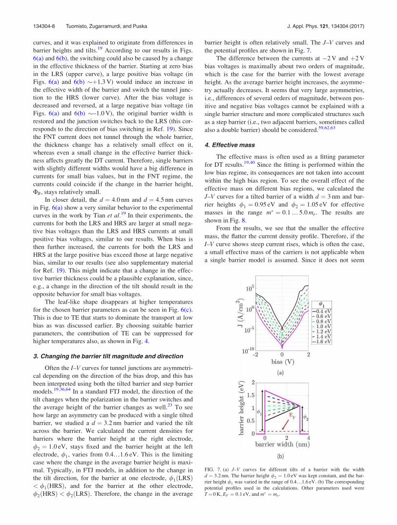
3. Changing the barrier tilt magnitude and direction
Often the I–V curves for tunnel junctions are asymmetri-
cal depending on the direction of the bias drop, and this has
been interpreted using both the tilted barrier and step barrier
models.19,36,64 In a standard FTJ model, the direction of the
tilt changes when the polarization in the barrier switches and
the average height of the barrier changes as well.23 To see
how large an asymmetry can be produced with a single tilted
barrier, we studied a d ¼ 3:2 nm barrier and varied the tilt
across the barrier. We calculated the current densities for
barriers where the barrier height at the right electrode,
/2 ¼ 1:0 eV, stays fixed and the barrier height at the left
electrode, /1, varies from 0:4…1:6 eV. This is the limiting
case where the change in the average barrier height is maxi-
mal. Typically, in FTJ models, in addition to the change in
the tilt direction, for the barrier at one electrode, /1ðLRSÞ< /1ðHRSÞ, and for the barrier at the other electrode,
/2ðHRSÞ < /2ðLRSÞ. Therefore, the change in the average
barrier height is often relatively small. The J–V curves and
the potential profiles are shown in Fig. 7.
The difference between the currents at �2 V and þ2 V
bias voltages is maximally about two orders of magnitude,
which is the case for the barrier with the lowest average
height. As the average barrier height increases, the asymme-
try actually decreases. It seems that very large asymmetries,
i.e., differences of several orders of magnitude, between pos-
itive and negative bias voltages cannot be explained with a
single barrier structure and more complicated structures such
as a step barrier (i.e., two adjacent barriers, sometimes called
also a double barrier) should be considered.59,62,63
4. Effective mass
The effective mass is often used as a fitting parameter
for DT results.19,40 Since the fitting is performed within the
low bias regime, its consequences are not taken into account
within the high bias region. To see the overall effect of the
effective mass on different bias regions, we calculated the
J–V curves for a tilted barrier of a width d ¼ 3 nm and bar-
rier heights /1 ¼ 0:95 eV and /2 ¼ 1:05 eV for effective
masses in the range m� ¼ 0:1 … 5:0 me. The results are
shown in Fig. 8.
From the results, we see that the smaller the effective
mass, the flatter the current density profile. Therefore, if the
I–V curve shows steep current rises, which is often the case,
a small effective mass of the carriers is not applicable when
a single barrier model is assumed. Since it does not seem
FIG. 7. (a) J–V curves for different tilts of a barrier with the width
d ¼ 3:2 nm. The barrier height /2 ¼ 1:0 eV was kept constant, and the bar-
rier height /1 was varied in the range of 0.4…1.6 eV. (b) The corresponding
potential profiles used in the calculations. Other parameters used were
T¼ 0 K, EF ¼ 0:1 eV, and m� ¼ me.
134304-8 Tuomisto, Zugarramurdi, and Puska J. Appl. Phys. 121, 134304 (2017)

reasonable that the effective mass would be strongly depen-
dent on the bias voltage, the implications of the magnitude
of the effective mass should be considered to check whether
the high bias results are compatible with the fitting within
the low-bias DT regime.
IV. CONCLUSIONS
We have modeled tunneling currents through layered
heterostructures using the Tsu-Esaki approach with numeri-
cally calculated transmission. The tilted barrier, including
image force lowering and rounding, was chosen as our model
potential since it is a simple structure, but yet, it has useful
applications, e:g:, for the modeling of FTJs. J–V curves
obtained using analytical formulae agree well with our calcu-
lations for thicker barriers for both low and high tempera-
tures. For thin barriers, the WKB approximation used in the
analytical formulae breaks down, whereas the numerically
solved transmission is accurate for extremely thin barriers as
well.
With our approach, we are able to produce the oscilla-
tions that do not show up when using the analytical formu-
lae. In addition, we can calculate the currents continuously
for a wide bias voltage range and for different Fermi energies
and temperatures in the electrodes. When using analytical
formulae for fitting, first the dominant tunneling process has
to be identified and, if more than one process needs to be
considered, the compatibility of the results from the different
fittings should be checked. With the Tsu-Esaki model, the fit-
ting can be performed at once for the whole bias range,
thereby avoiding these considerations.
In order to show what kind of I–V curve features are
reproducible by using a single tilted barrier model, we calcu-
lated currents for different tilts and widths of the barrier.
According to our results, in asymmetrical I–V curves, differ-
ences of about two orders of magnitude can be explained by
a change in the tilt of the barrier. Asymmetries of several
orders of magnitude in current, which have been observed in
experiments, require the use of a more complicated barrier
model such as a step barrier. We also found that the currents
may increase with increasing barrier thickness if barrier
rounding due to, e.g., image force lowering, is taken into
account and a constant electric field within the barrier is
assumed.
As a slightly unexpected phenomenon for the simple
tilted barrier model, we discovered in our simulations a
“leaf-like” shape, which is also observed in certain experi-
mental I–V curves. According to the modeling, it can be
explained by a small change in the effective thickness of the
tunnel barrier rather than changes in the barrier height or tilt.
In this model, two different effective widths correspond to
two different resistance states and the characteristics of the
calculated currents are similar to the experimental data in
both low and high bias voltage regions.
Our results give guidelines for the use of analytical for-
mulae for fitting and provide a useful tool for distinguishing
features related to single barrier structures in experimental
I–V curves. In the future, we will look at currents through
step barrier structures, enabling the study of resonance
effects and more complicated I–V curve features.
ACKNOWLEDGMENTS
The authors would like to thank Professor Sebastiaan
van Dijken for fruitful discussions and for his help in the
preparation of the manuscript. This work was supported by
the Academy of Finland through its Centres of Excellence
Programme (2012-2017) under Project No. 251748.
1C. B. Duke, Tunneling in Solids (Academic Press, New York, 1969).2E. L. Wolf, Principles of Electron Tunneling Spectroscopy (Oxford
University Press, New York, 1985).3V. Garcia and M. Bibes, Nat. Commun. 5, 4289 (2014).4R. H. Fowler and L. Nordheim, Proc. R. Soc. London, Ser. A 119, 173
(1928).5J. G. Simmons, J. Appl. Phys. 34, 1793 (1963).6S. M. Sze and K. K. Ng, Physics of Semiconductor Devices, 3rd ed.
(Wiley-Interscience, Hoboken, 2007).7W. J. Chang, M. P. Houng, and Y. H. Wang, J. Appl. Phys. 89, 6285
(2001).8D. Ielmini, A. S. Spinelli, M. A. Rigamonti, and A. L. Lacaita, IEEE
Trans. Electron Devices 47, 1258 (2000).9D. Ielmini, A. S. Spinelli, M. A. Rigamonti, and A. L. Lacaita, IEEE
Trans. Electron Devices 47, 1266 (2000).10F. Jim�enez-Molinos, A. Palma, F. G�amiz, J. Banqueri, and J. A. L�opez-
Villanueva, J. Appl. Phys. 90, 3396 (2001).11D. K. Ferry and S. M. Goodnick, Transport in Nanostructures (Cambridge
University Press, Cambridge, UK, 1997).12J. Bardeen, Phys. Rev. Lett. 6, 57 (1961).13S. Datta, Electronic Transport in Mesoscopic Systems (Cambridge
University Press, New York, 1995).14R. Tsu and L. Esaki, Appl. Phys. Lett. 22, 562 (1973).15C. S. Lent and D. J. Kirkner, J. Appl. Phys. 67, 6353 (1990).16D. Pantel and M. Alexe, Phys. Rev. B 82, 134105 (2010).17S. Boyn, V. Garcia, S. Fusil, C. Carr�et�ero, K. Garcia, S. Xavier, S. Collin,
C. Deranlot, M. Bibes, and A. Barth�el�emy, APL Mater. 3, 061101 (2015).18H. Yamada, A. Tsurumaki-Fukuchi, M. Kobayashi, T. Nagai, Y.
Toyosaki, H. Kumigashira, and A. Sawa, Adv. Funct. Mater. 25, 2708
(2015).19B. B. Tian, J. L. Wang, S. Fusil, Y. Liu, X. L. Zhao, S. Sun, H. Shen, T.
Lin, J. L. Sun, C. G. Duan, M. Bibes, A. Barth�el�emy, B. Dkhil, V. Garcia,
X. J. Meng, and J. H. Chu, Nat. Commun. 7, 11502 (2016).20M. Bibes, J. E. Villegas, and A. Barth�el�emy, Adv. Phys. 60, 5 (2011).21E. Tsymbal, A. Gruverman, V. Garcia, M. Bibes, and A. Barth�el�emy,
MRS Bull. 37, 138 (2012).22H. Kohlstedt, N. Pertsev, J. Rodr�ıguez Contreras, and R. Waser, Phys.
Rev. B 72, 125341 (2005).23M. Zhuravlev, R. Sabirianov, S. Jaswal, and E. Tsymbal, Phys. Rev. Lett.
94, 246802 (2005).24E. Y. Tsymbal and H. Kohlstedt, Science 313, 181 (2006).
FIG. 8. J–V curves for different effective electron masses (m�
¼ 0:1…5:0 meÞ. Barrier heights /1¼ 0.95 eV and /2¼ 1.05 eV, and a bar-
rier width of d ¼ 3 nm are used. Moreover, T¼ 0 K and EF ¼ 0:1 eV are
assumed.
134304-9 Tuomisto, Zugarramurdi, and Puska J. Appl. Phys. 121, 134304 (2017)

25J. Velev, C.-G. Duan, K. Belashchenko, S. Jaswal, and E. Tsymbal, Phys.
Rev. Lett. 98, 137201 (2007).26J. P. Velev, C.-G. Duan, J. D. Burton, A. Smogunov, M. K. Niranjan, E.
Tosatti, S. S. Jaswal, and E. Y. Tsymbal, Nano Lett. 9, 427 (2009).27X. Liu, Y. Wang, J. D. Burton, and E. Y. Tsymbal, Phys. Rev. B 88,
165139 (2013).28V. S. Borisov, S. Ostanin, S. Achilles, J. Henk, and I. Mertig, Phys. Rev. B
92, 075137 (2015).29L. L. Tao and J. Wang, Appl. Phys. Lett. 108, 062903 (2016).30P. Maksymovych, S. Jesse, P. Yu, R. Ramesh, A. P. Baddorf, and S. V.
Kalinin, Science 324, 1421 (2009).31A. Zenkevich, M. Minnekaev, Y. Matveyev, Y. Lebedinskii, K. Bulakh,
A. Chouprik, A. Baturin, K. Maksimova, S. Thiess, and W. Drube, Appl.
Phys. Lett. 102, 062907 (2013).32R. Soni, A. Petraru, P. Meuffels, O. Vavra, M. Ziegler, S. K. Kim, D. S.
Jeong, N. A. Pertsev, and H. Kohlstedt, Nat. Commun. 5, 5414 (2014).33L. Jiang, W. S. Choi, H. Jeen, S. Dong, Y. Kim, M.-G. Han, Y. Zhu, S. V.
Kalinin, E. Dagotto, T. Egami, and H. N. Lee, Nano Lett. 13, 5837 (2013).34Z. Wen, C. Li, D. Wu, A. Li, and N. Ming, Nat. Mater. 12, 617 (2013).35G. Radaelli, D. Guti�errez, F. S�anchez, R. Bertacco, M. Stengel, and J.
Fontcuberta, Adv. Mater. 27, 2602 (2015).36Q. H. Qin, L. €Ak€aslompolo, N. Tuomisto, L. Yao, S. Majumdar, J.
Vijayakumar, A. Casiraghi, S. Inkinen, B. Chen, A. Zugarramurdi, M.
Puska, and S. van Dijken, Adv. Mater. 28, 6852 (2016).37Z. Wen, L. You, J. Wang, A. Li, and D. Wu, Appl. Phys. Lett. 103,
132913 (2013).38M. Koberidze, A. V. Feshchenko, M. J. Puska, R. M. Nieminen, and J. P.
Pekola, J. Phys. D: Appl. Phys. 49, 165303 (2016).39J. Tersoff, Phys. Rev. Lett. 52, 465 (1984).40A. Quindeau, V. Borisov, I. Fina, S. Ostanin, E. Pippel, I. Mertig, D.
Hesse, and M. Alexe, Phys. Rev. B 92, 035130 (2015).41A. Schenk and G. Heiser, J. Appl. Phys. 81, 7900 (1997).42A. Gehring and S. Selberherr, IEEE Trans. Device Mater. Reliab. 4, 306
(2004).43Z. A. Weinberg, J. Appl. Phys. 53, 5052 (1982).
44W. Y. Quan, D. M. Kim, and M. K. Cho, J. Appl. Phys. 92, 3724 (2002).45E. I. Goldman, N. F. Kukharskaya, and A. G. Zhdan, Solid. State.
Electron. 48, 831 (2004).46J. C. Ranu�arez, M. J. Deen, and C. H. Chen, Microelectron. Reliab. 46,
1939 (2006).47B. A. Politzer, J. Appl. Phys. 37, 279 (1966).48M. O. Vassell, J. Lee, and H. F. Lockwood, J. Appl. Phys. 54, 5206
(1983).49W. W. Lui and M. Fukuma, J. Appl. Phys. 60, 1555 (1986).50Y. Ando and T. Itoh, J. Appl. Phys. 61, 1497 (1987).51E. Hairer, S. P. Norsett, and G. Wanner, Solving Ordinary Differential
Equations. I. Nonstiff Problems, 2nd ed. (Springer-Verlag, Berlin, 1993).52J. L. M. Quiroz Gonz�alez and D. Thompson, Comput. Phys. 11, 514
(1997).53W. H. Press, S. A. Teukolsky, W. T. Vetterling, and B. P. Flannery,
Numerical Recipes in FORTRAN: The Art of Scientific Computing, 2nd ed.
(Cambridge University Press, Cambridge, 1992), Sec. 16.2.54J. G. Simmons, J. Appl. Phys. 34, 2581 (1963).55A. Gruverman, D. Wu, H. Lu, Y. Wang, H. W. Jang, C. M. Folkman, M.
Y. Zhuravlev, D. Felker, M. Rzchowski, C.-B. Eom, and E. Y. Tsymbal,
Nano Lett. 9, 3539 (2009).56E. W. Cowell, S. W. Muir, D. A. Keszler, and J. F. Wager, J. Appl. Phys.
114, 213703 (2013).57W. F. Brinkman, R. C. Dynes, and J. M. Rowell, J. Appl. Phys. 41, 1915
(1970).58H. Von Wenckstern, G. Biehne, R. A. Rahman, H. Hochmuth, M. Lorenz,
and M. Grundmann, Appl. Phys. Lett. 88, 092102 (2006).59S. Grover and G. Moddel, Solid State Electron. 67, 94 (2012).60M. V. Fischetti, J. Appl. Phys. 93, 3123 (2003).61W. Y. Quan, D. M. Kim, and M. K. Cho, J. Appl. Phys. 93, 3125 (2003).62P. A. Schulz and C. E. T. Goncalves da Silva, Appl. Phys. Lett. 52, 960
(1988).63X. Liu, J. Burton, and E. Y. Tsymbal, Phys. Rev. Lett. 116, 197602
(2016).64N. Alimardani and J. F. Conley, Appl. Phys. Lett. 102, 143501 (2013).
134304-10 Tuomisto, Zugarramurdi, and Puska J. Appl. Phys. 121, 134304 (2017)