Embed Size (px)
Citation preview
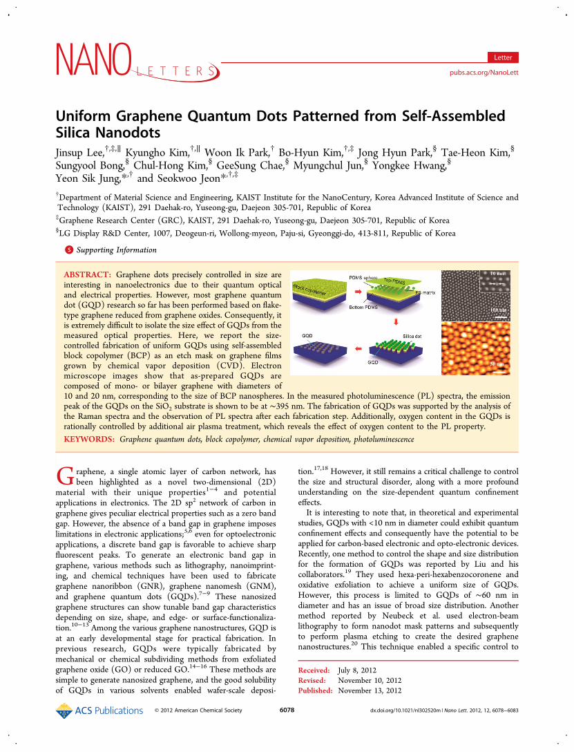
Uniform Graphene Quantum Dots Patterned from Self-AssembledSilica NanodotsJinsup Lee,†,‡,∥ Kyungho Kim,†,∥ Woon Ik Park,† Bo-Hyun Kim,†,‡ Jong Hyun Park,§ Tae-Heon Kim,§
Sungyool Bong,§ Chul-Hong Kim,§ GeeSung Chae,§ Myungchul Jun,§ Yongkee Hwang,§
Yeon Sik Jung,*,† and Seokwoo Jeon*,†,‡
†Department of Material Science and Engineering, KAIST Institute for the NanoCentury, Korea Advanced Institute of Science andTechnology (KAIST), 291 Daehak-ro, Yuseong-gu, Daejeon 305-701, Republic of Korea‡Graphene Research Center (GRC), KAIST, 291 Daehak-ro, Yuseong-gu, Daejeon 305-701, Republic of Korea§LG Display R&D Center, 1007, Deogeun-ri, Wollong-myeon, Paju-si, Gyeonggi-do, 413-811, Republic of Korea
*S Supporting Information
ABSTRACT: Graphene dots precisely controlled in size areinteresting in nanoelectronics due to their quantum opticaland electrical properties. However, most graphene quantumdot (GQD) research so far has been performed based on flake-type graphene reduced from graphene oxides. Consequently, itis extremely difficult to isolate the size effect of GQDs from themeasured optical properties. Here, we report the size-controlled fabrication of uniform GQDs using self-assembledblock copolymer (BCP) as an etch mask on graphene filmsgrown by chemical vapor deposition (CVD). Electronmicroscope images show that as-prepared GQDs arecomposed of mono- or bilayer graphene with diameters of10 and 20 nm, corresponding to the size of BCP nanospheres. In the measured photoluminescence (PL) spectra, the emissionpeak of the GQDs on the SiO2 substrate is shown to be at ∼395 nm. The fabrication of GQDs was supported by the analysis ofthe Raman spectra and the observation of PL spectra after each fabrication step. Additionally, oxygen content in the GQDs isrationally controlled by additional air plasma treatment, which reveals the effect of oxygen content to the PL property.
KEYWORDS: Graphene quantum dots, block copolymer, chemical vapor deposition, photoluminescence
Graphene, a single atomic layer of carbon network, hasbeen highlighted as a novel two-dimensional (2D)
material with their unique properties1−4 and potentialapplications in electronics. The 2D sp2 network of carbon ingraphene gives peculiar electrical properties such as a zero bandgap. However, the absence of a band gap in graphene imposeslimitations in electronic applications;5,6 even for optoelectronicapplications, a discrete band gap is favorable to achieve sharpfluorescent peaks. To generate an electronic band gap ingraphene, various methods such as lithography, nanoimprint-ing, and chemical techniques have been used to fabricategraphene nanoribbon (GNR), graphene nanomesh (GNM),and graphene quantum dots (GQDs).7−9 These nanosizedgraphene structures can show tunable band gap characteristicsdepending on size, shape, and edge- or surface-functionaliza-tion.10−13 Among the various graphene nanostructures, GQD isat an early developmental stage for practical fabrication. Inprevious research, GQDs were typically fabricated bymechanical or chemical subdividing methods from exfoliatedgraphene oxide (GO) or reduced GO.14−16 These methods aresimple to generate nanosized graphene, and the good solubilityof GQDs in various solvents enabled wafer-scale deposi-
tion.17,18 However, it still remains a critical challenge to controlthe size and structural disorder, along with a more profoundunderstanding on the size-dependent quantum confinementeffects.It is interesting to note that, in theoretical and experimental
studies, GQDs with <10 nm in diameter could exhibit quantumconfinement effects and consequently have the potential to beapplied for carbon-based electronic and opto-electronic devices.Recently, one method to control the shape and size distributionfor the formation of GQDs was reported by Liu and hiscollaborators.19 They used hexa-peri-hexabenzocoronene andoxidative exfoliation to achieve a uniform size of GQDs.However, this process is limited to GQDs of ∼60 nm indiameter and has an issue of broad size distribution. Anothermethod reported by Neubeck et al. used electron-beamlithography to form nanodot mask patterns and subsequentlyto perform plasma etching to create the desired graphenenanostructures.20 This technique enabled a specific control to
Received: July 8, 2012Revised: November 10, 2012Published: November 13, 2012
Letter
pubs.acs.org/NanoLett
© 2012 American Chemical Society 6078 dx.doi.org/10.1021/nl302520m | Nano Lett. 2012, 12, 6078−6083
achieve a narrow size distribution of GQDs. However, GQDsbased on e-beam lithography and other top-down approachesface critical challenges such as low throughput and poorproperties. Nevertheless, the synergic combination of CVDgrowth of graphene and high-throughput patterning methodsthat can precisely control the size of GQDs may offer anexcellent opportunity to study the optical properties of GQDs.Herein, we propose a new route for the fabrication of
uniform-sized GQDs, in which a BCP self-assembly process isadopted to control the size of GQDs as small as 10 and 20 nm.In our previous studies, uniform and robust nanoscale silica dotpatterns were formed from Si-containing polystyrene-b-
polydimethylsiloxane (PS-PDMS) block copolymers (BCPs).BCP self-assembly has been investigated as a way of highlyscalable nanofabrication with ultrahigh resolution.21−23 Uni-form BCP self-assembly was realized on PDMS-functionalizedgraphene, and the patterned silica nanodots of PS-PDMS BCPwere used as an etch mask for the fabrication of GQDs. Thevariable diameter of silica nanodots, depending on themolecular weight of the BCP, allowed the precise control ofthe size of the GQDs. Both monolayer GQDs formed on an Sisubstrate and dispersed GQDs in an aqueous solution showblue emissions at 395 nm under excitation with a 325 nm He−Cd laser; the adjusted PL spectra also exhibited wavelength
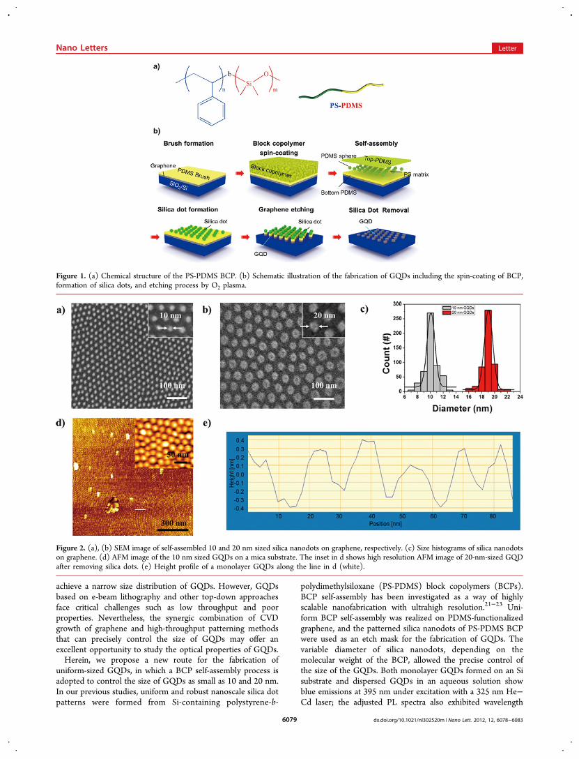
Figure 1. (a) Chemical structure of the PS-PDMS BCP. (b) Schematic illustration of the fabrication of GQDs including the spin-coating of BCP,formation of silica dots, and etching process by O2 plasma.
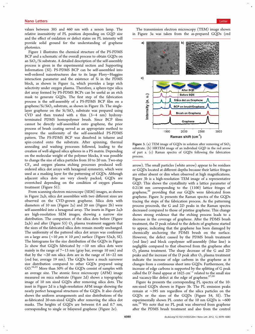
Figure 2. (a), (b) SEM image of self-assembled 10 and 20 nm sized silica nanodots on graphene, respectively. (c) Size histograms of silica nanodotson graphene. (d) AFM image of the 10 nm sized GQDs on a mica substrate. The inset in d shows high resolution AFM image of 20-nm-sized GQDafter removing silica dots. (e) Height profile of a monolayer GQDs along the line in d (white).
Nano Letters Letter
dx.doi.org/10.1021/nl302520m | Nano Lett. 2012, 12, 6078−60836079
values between 385 and 460 nm with a xenon lamp. Therelative insensitivity of PL position depending on GQD sizeand the effect of oxidation or defect states on PL intensity willprovide solid ground for the understanding of graphenephotonics.Figure 1 illustrates the chemical structure of the PS-PDMS
BCP and a schematic of the overall process to obtain GQDs onan SiO2/Si substrate. A detailed description of the self-assemblyprocess is given in the experimental section and SupportingInformation (SI). PS-PDMS BCP can be self-assembled intowell-ordered nanostructures due to its large Flory−Hugginsinteraction parameter and the existence of Si in the PDMSblock, as shown in Figure 1a, which provides a large etchselectivity under oxygen plasma. Therefore, a sphere-type silicadot array formed by PS-PDMS BCPs can be useful as an etchmask to generate GQDs. The first step of the fabricationprocess is the self-assembly of a PS-PDMS BCP film on agraphene/Si/SiO2 substrate, as shown in Figure 1b. The single-layer graphene on the Si/SiO2 substrate was prepared usingCVD and then treated with a thin (3−4 nm) hydroxy-terminated PDMS homopolymer brush. Since BCP filmscannot be directly self-assembled onto graphene, the priorprocess of brush coating served as an appropriate method toimprove the uniformity of the self-assembled PS-PDMSpattern. The PS-PDMS BCP was dissolved in toluene andspin-coated onto the substrate. After spinning, thermalannealing and washing processes followed, leading to thecreation of well-aligned silica spheres in a PS matrix. Dependingon the molecular weight of the polymer blocks, it was possibleto change the size of silica particles from 10 to 20 nm. Two-stepCF4 and oxygen plasma etching processes produced well-ordered silica dot arrays with hexagonal symmetry, which wereused as a masking layer for the patterning of GQDs. Althoughadjacent silica dots are very closely packed, GQDs areoveretched depending on the condition of oxygen plasmatreatment (Figure S1).From scanning electron microscope (SEM) images, as shown
in Figure 2a,b, silica dot assemblies with two different sizes areobserved on the CVD-grown graphene. Silica dots withdiameters of 10 nm (Figure 2a) and 20 nm (Figure 2b) wereself-assembled into a hexagonal array. The insets in Figure 2a,bare high-resolution SEM images, showing a narrow sizedistribution. The comparison of the silica dots before (Figure2a,b) and after (Figure S3) O2 plasma treatment suggests thatthe sizes of the fabricated silica dots remain mostly unchanged.The uniformity of the pattered silica dot arrays was confirmedon a large area (∼10 μm × 10 μm) surface (Figure S3a,b, SI).The histograms for the size distribution of the GQDs in Figure2c show that GQDs fabricated by ∼10 nm silica dots weremainly in the range of 7−13 nm (gray bar, average 10 nm) andthat by the ∼20 nm silica dots are in the range of 16−22 nm(red bar, average 19 nm). The GQDs have a much narrowersize distribution compared to other GQDs prepared usingGO.24,25 More than 50% of the GQDs consist of samples withan average size. The atomic force microscopy (AFM) imagemeasured on mica substrate (Figure 2d) shows a topographicimage of 10 nm sized GQDs after removing silica dots. Theinset in Figure 2d is a high-resolution AFM image showing thenearly perfect hexagonal structures of the GQDs. It also clearlyshows the uniform arrangements and size distributions of theas-fabricated 20-nm-sized GQDs after removing the silica dotmasks. The heights of GQDs are between 0.4 and 0.7 nm,corresponding to single or bilayered graphene (Figure 2e).
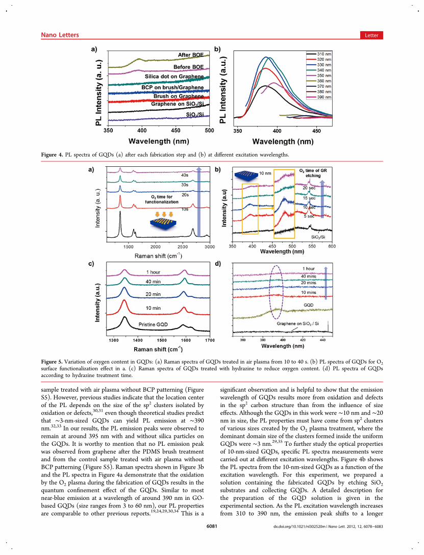
The transmission electron microscopy (TEM) image shownin Figure 3a was taken from the as-prepared GQDs (red
arrow). The small particles (white arrow) appear to be residuesor GQDs located at different depths because their lattice fringesare either absent or dim when observed at high magnifications.Figure 3b is a high-resolution TEM image of a representativeGQD. This shows the crystallinity with a lattice parameter of0.2136 nm corresponding to the (1100) lattice fringes ofgraphene,26 providing that our GQDs were fabricated fromgraphene. Figure 3c presents the Raman spectra of the GQDstracing the steps of the fabrication process. As the patterningprocess proceeds, the G and 2D peaks in the Raman spectradecreased compared to those of pristine graphene. This changeshows strong evidence that the etching process leads to adecrease in the coverage of graphene. After the PDMS brushtreatment, the D peak related to the defects of graphene startedto appear, indicating that the graphene has been damaged bychemically anchoring the PDMS brush on the surface.However, the defect caused by the PDMS brush treatment(red line) and block copolymer self-assembly (blue line) isnegligible compared to that observed from the graphene afterO2 plasma treatment. The sharp decrease of the G and 2Dpeaks and the increase of the D peak after O2 plasma treatmentindicate the increase of edge carbons in the graphene as itchanges from a continuous sheet into GQDs. Furthermore, theincrease of edge carbons is supported by the splitting of G peakcalled the D′-band appear at 1625 cm−1 related to the small sizeand vacancy-like defect at the edge of graphene.27,28
Figure 4a presents the corresponding PL spectra of the 10-nm-sized GQDs shown in Figure 3b. The PL emission peaksremain at ∼395 nm regardless of the silica particles on theGQDs or the sizes of the GQDs (Figure S4, SI). Theexperimentally shown PL center of the 10 nm GQDs is ∼600nm.29 We note that no PL peak was observed from grapheneafter the PDMS brush treatment and also from the control
Figure 3. (a) TEM image of GQDs in solution after removing of SiO2substrate. (b) HRTEM image of an individual GQD in the red arrowof part a. (c) Raman spectra of GQDs following the fabricationprocess.
Nano Letters Letter
dx.doi.org/10.1021/nl302520m | Nano Lett. 2012, 12, 6078−60836080
sample treated with air plasma without BCP patterning (FigureS5). However, previous studies indicate that the location centerof the PL depends on the size of the sp2 clusters isolated byoxidation or defects,30,31 even though theoretical studies predictthat ∼3-nm-sized GQDs can yield PL emission at ∼390nm.32,33 In our results, the PL emission peaks were observed toremain at around 395 nm with and without silica particles onthe GQDs. It is worthy to mention that no PL emission peakwas observed from graphene after the PDMS brush treatmentand from the control sample treated with air plasma withoutBCP patterning (Figure S5). Raman spectra shown in Figure 3band the PL spectra in Figure 4a demonstrate that the oxidationby the O2 plasma during the fabrication of GQDs results in thequantum confinement effect of the GQDs. Similar to mostnear-blue emission at a wavelength of around 390 nm in GO-based GQDs (size ranges from 3 to 60 nm), our PL propertiesare comparable to other previous reports.19,24,29,30,34 This is a
significant observation and is helpful to show that the emissionwavelength of GQDs results more from oxidation and defectsin the sp2 carbon structure than from the influence of sizeeffects. Although the GQDs in this work were ∼10 nm and ∼20nm in size, the PL properties must have come from sp2 clustersof various sizes created by the O2 plasma treatment, where thedominant domain size of the clusters formed inside the uniformGQDs were ∼3 nm.29,35 To further study the optical propertiesof 10-nm-sized GQDs, specific PL spectra measurements werecarried out at different excitation wavelengths. Figure 4b showsthe PL spectra from the 10-nm-sized GQDs as a function of theexcitation wavelength. For this experiment, we prepared asolution containing the fabricated GQDs by etching SiO2
substrates and collecting GQDs. A detailed description forthe preparation of the GQD solution is given in theexperimental section. As the PL excitation wavelength increasesfrom 310 to 390 nm, the emission peak shifts to a longer
Figure 4. PL spectra of GQDs (a) after each fabrication step and (b) at different excitation wavelengths.
Figure 5. Variation of oxygen content in GQDs: (a) Raman spectra of GQDs treated in air plasma from 10 to 40 s. (b) PL spectra of GQDs for O2surface functionalization effect in a. (c) Raman spectra of GQDs treated with hydrazine to reduce oxygen content. (d) PL spectra of GQDsaccording to hydrazine treatment time.
Nano Letters Letter
dx.doi.org/10.1021/nl302520m | Nano Lett. 2012, 12, 6078−60836081
wavelength, from 373 nm (black) to 456 nm (pink). A similartendency also appeared for the GQDs fabricated by GO.30,34
In both sets of results shown in Figures 3 and 4, it isrecognized that oxygen defects can be formed on GQDs, whichformation causes the variation of the Raman spectra and the PLemission. To prove the effect of oxygen at the surface of theGQDs, controlled oxidation and reduction were performed onthe GQDs by air plasma and hydrazine (Figure 5). From thestudy of the Raman spectroscopy of the GQDs treatedadditionally with plasma (Figure 5a), it was found that, withincreasing treatment time, the whole peak intensity decreased.A detailed composition analysis after air plasma treatment (15s, 65% carbon ratio) and reduction treatment (10 min, 78%carbon ratio) was carried out using X-ray photoelectronspectroscopy (XPS) measurements (Figure S7 in SI). Theratio of ID/IG measured from all peaks, which is known to berelated to the defect length of graphene, showed its greatestvalue between 10 and 20 s.36 Since the formed GQDs were 10nm in diameter, if the domain size of the GQDs is estimated tobe less than 5 nm, it implies that the graphene structures arebroken and torn by the air plasma treatment. The effect of airplasma surface treatment on GQDs shows no peak-shift,whereas the PL intensity declined after additional air plasmatreatment for 10 s (Figure 5b). This shows that the componentratio of oxygen in GQDs can be optimized for the strongest PLemission. Moreover, excessive etching leads to additionaldefects and an increase of oxygen to carbon ratio in GQDs,resulting in the collapse of the 10-nm-sized sp2 carbon structurein GQDs.30,37,38 Similar results can also be observed for largerGQDs (Figure S4). Furthermore, we investigated the influenceof substrate functionalization on the PL emission characteristicsof GQDs. As shown in Figure S6, slight variations (∼10 nm) ofPL peak positions depending on self-assembled monolayer(SAM) molecules were observed. This suggests that the surfacetreatment of substrates can provide a tool to tune the emissionspectra of GQDs.Likewise, an interesting phenomenon was observed in
hydrazine-treated GQDs (Figure 5c). In the Raman spectraand XPS measurement, deoxidized GQDs showed improvedquality with increasing hydrazine treatment time due to theenhancement of the IG/I2D ratio. Nevertheless, the hydrazine-treated GQDs release weaker luminescence at the near-bluewavelength compared to nontreated GQDs. The correspondingPL spectra of the GQDs after each incremental reductiontreatment (from 10 min up to 1 h) are shown in Figure 5d. ThePL intensity was very weak due to the fabrication process thatused only single layer graphene with low areal density ofGQDs. The highest tendency of the luminescent spectrum is anemissive steady ratio of oxygen on the Si/SiO2 substrate, whichresult is similar to a previous report by Eda et al.30 In this study,however, due to GQDs composed of single layer graphene, ithas received a lot of reduction effect through hydrazinetreatments in a short time. Since we performed plasma andhydrazine treatment from GQDs, we expect that proper oxygencontents can be controlled to the intensity of the PL, along withthe quenching effect.In summary, we demonstrated the first PL study of uniform
GQDs on Si/SiO2 substrate and aqueous solution. Wedescribed a controllable and scalable fabrication method for10 and 20 nm GQDs from single-layer CVD grown grapheneusing self-assembled BCP. GQDs were fabricated on the CVDgrown graphene using silica nanodots created from self-assembled PS-PDMS block-copolymer as an etching mask.
The fabricated GQDs show a hexagonal arrangement with anarrow size distribution; this arrangement is superior to thosepresented in previous studies. GQDs shows PL emission at 395nm on the SiO2 substrate, and this is comparable to otherGQDs fabricated from GO. In the case of 10-nm-sized GQDs,we experimentally showed that the actual PL spectracorrespond to near-blue emission instead of red emission.The observation of significant oxidation and defect value inGQDs will be important for the control and enhancement ofoptoelectronic properties. Finally, we believe our researchprovides a noteworthy contribution to enhancing the propertiesof GQDs and to the understanding of the effects of size andfunctionalization on GQDs.
■ ASSOCIATED CONTENT*S Supporting InformationExperimental details such as graphene growth and transfermethods, fabrication of GQDs, and characterization tools.Additional GQD characterization data including Ramanspectra, SEM image, and XPS results. This material is availablefree of charge via the Internet at http://pubs.acs.org.
■ AUTHOR INFORMATIONCorresponding Author*E-mail: [email protected]; [email protected] Contributions∥These authors contributed equally to this work.NotesThe authors declare no competing financial interest.
■ ACKNOWLEDGMENTSThis work was supported by the Converging Research CenterProgram through the National Research Foundation of Korea(NRF) funded by the Ministry of Education, Science andTechnology (2011K000623). It was also partially supported bythe Future-based Technology Development Program (NanoFields) through the National Research Foundation of Korea(NRF) funded by the Ministry of Education, Science andTechnology (2010-0029332) and through a grant (2011-0031630) from the Center for Advanced Soft Electronics underthe Global Frontier Research Program of the Ministry ofEducation, Science and Technology, Korea. This research wasalso supported by the GRC project of KAIST Institute for theNanoCentury.
■ REFERENCES(1) Stankovich, S.; Dikin, D. A.; Dommett, G. H. B.; Kohlhaas, K. M.;Zimney, E. J.; Stach, E. A.; Piner, R. D.; Nguyen, S. T.; Ruoff, R. S.Nature 2006, 442, 282−286.(2) Geim, A. K.; Novoselov, K. S. Nat. Mater. 2007, 6, 183−191.(3) Geim, A. K. Science 2009, 324, 1530−1534.(4) Ponomarenko, L. A.; Schedin, F.; Katsnelson, M. I.; Yang, R.;Hill, E. W.; Novoselov, K. S.; Geim, A. K. Science 2008, 320, 356−358.(5) Novoselov, K. S.; Geim, A. K.; Morozov, S. V.; Jiang, D.; Zhang,Y.; Dubonos, S. V.; Grigorieva, I. V.; Firsov, A. A. Science 2004, 306,666−669.(6) Nakada, K.; Fujita, M.; Dresselhaus, G.; Dresselhaus, M. S. Phys.Rev. B 1996, 54, 17954−17961.(7) Li, X. L.; Wang, X. R.; Zhang, L.; Lee, S. W.; Dai, H. J. Science2008, 319, 1229−1232.(8) Bai, J. W.; Zhong, X.; Jiang, S.; Huang, Y.; Duan, X. F. Nat.Nanotechnol. 2010, 5, 190−194.(9) Tang, C. L.; Yan, W. H.; Zheng, Y. S.; Li, G. S.; Li, L. P.Nanotechnology 2008, 19.
Nano Letters Letter
dx.doi.org/10.1021/nl302520m | Nano Lett. 2012, 12, 6078−60836082
(10) Wang, Z. F.; Shi, Q. W.; Chen, J. J. Nanosci. Nanotechnol. 2009,9, 4580−4585.(11) Wang, L. J.; Li, H. O.; Tu, T.; Cao, G.; Zhou, C.; Hao, X. J.; Su,Z.; Xiao, M.; Guo, G. C.; Chang, A. M.; Guo, G. P. Appl. Phys. Lett.2012, 100.(12) Gupta, V.; Chaudhary, N.; Srivastava, R.; Sharma, G. D.;Bhardwaj, R.; Chand, S. J. Am. Chem. Soc. 2011, 133, 9960−9963.(13) Pereira, J. M.; Vasilopoulos, P.; Peeters, F. M. Nano Lett. 2007,7, 946−949.(14) Moriyama, S.; Tsuya, D.; Watanabe, E.; Uji, S.; Shimizu, M.;Mori, T.; Yamaguchi, T.; Ishibashi, K. Nano Lett. 2009, 9, 2891−2896.(15) Ritter, K. A.; Lyding, J. W. Nat. Mater. 2009, 8, 235−242.(16) Zhuo, S. J.; Shao, M. W.; Lee, S. T. ACS Nano 2012, 6, 1059−1064.(17) Zhu, S. J.; Zhang, J. H.; Liu, X.; Li, B.; Wang, X. F.; Tang, S. J.;Meng, Q. N.; Li, Y. F.; Shi, C.; Hu, R.; Yang, B. Roy. Soc. Chem. Adv.2012, 2, 2717−2720.(18) Pan, D. Y.; Guo, L.; Zhang, J. C.; Xi, C.; Xue, Q.; Huang, H.; Li,J. H.; Zhang, Z. W.; Yu, W. J.; Chen, Z. W.; Li, Z.; Wu, M. H. J. Mater.Chem. 2012, 22, 3314−3318.(19) Liu, R. L.; Wu, D. Q.; Feng, X. L.; Mullen, K. J. Am. Chem. Soc.2011, 133, 15221−15223.(20) Neubeck, S.; Ponomarenko, L. A.; Freitag, F.; Giesbers, A. J. M.;Zeitler, U.; Morozov, S. V.; Blake, P.; Geim, A. K.; Novoselov, K. S.Small 2010, 6, 1469−1473.(21) Jung, Y. S.; Ross, C. A. Adv. Mater. 2009, 21, 2540−2545.(22) Jung, Y. S.; Ross, C. A. Small 2009, 5, 1654−1659.(23) Jeong, J. W.; Park, W. I.; Kim, M. J.; Ross, C. A.; Jung, Y. S.Nano Lett. 2011, 11, 4095−4101.(24) Pan, D. Y.; Zhang, J. C.; Li, Z.; Wu, M. H. Adv. Mater. 2010, 22,734−738.(25) Shen, J. H.; Zhu, Y. H.; Yang, X. L.; Zong, J.; Zhang, J. M.; Li, C.Z. New J. Chem. 2012, 36, 97−101.(26) Park, S.; An, J.; Piner, R. D.; Jung, I.; Yang, D.; Velamakanni, A.;Nguyen, S. T.; Ruoff, R. S. Chem. Mater. 2008, 20, 6592−6594.(27) Eckmann, A.; Felten, A.; Mishchenko, A.; Britnell, L.; Krupke,R.; Novoselov, K. S.; Casiraghi, C. Nano Lett. 2012, 12, 3925−3930.(28) Ryu, S.; Maultzsch, J.; Han, M. Y.; Kim, P.; Brus, L. E. ACSNano 2011, 5, 4123−4130.(29) Peng, J.; Gao, W.; Gupta, B. K.; Liu, Z.; Romero-Aburto, R.; Ge,L. H.; Song, L.; Alemany, L. B.; Zhan, X. B.; Gao, G. H.; Vithayathil, S.A.; Kaipparettu, B. A.; Marti, A. A.; Hayashi, T.; Zhu, J. J.; Ajayan, P.M. Nano Lett. 2012, 12, 844−849.(30) Eda, G.; Lin, Y. Y.; Mattevi, C.; Yamaguchi, H.; Chen, H. A.;Chen, I. S.; Chen, C. W.; Chhowalla, M. Adv. Mater. 2010, 22, 505−509.(31) Mattevi, C.; Eda, G.; Agnoli, S.; Miller, S.; Mkhoyan, K. A.;Celik, O.; Mostrogiovanni, D.; Granozzi, G.; Garfunkel, E.; Chhowalla,M. Adv. Funct. Mater. 2009, 19, 2577−2583.(32) Rusli; Robertson, J.; Amaratunga, G. A. J. J. Appl. Phys. 1996, 80,2998−3003.(33) Boukhvalov, D. W.; Katsnelson, M. I. J. Am. Chem. Soc. 2008,130, 10697−10701.(34) Shen, J. H.; Zhu, Y. H.; Chen, C.; Yang, X. L.; Li, C. Z. Chem.Commun. 2011, 47, 2580−2582.(35) Sun, Y.; Zhou, B.; Lin, Y.; Wang, W.; Fernando, K. A. S.; Pathak,P.; Meziani, M. J.; Harruff, B. A.; Wang, X.; Wang, H.; Luo, P. G.;Yang, H.; Kose, M. E.; Chen, B.; Veca, L. M.; Xie, S. J. Am. Chem. Soc.2006, 128, 7756−7757.(36) Jorio, A.; Ferreira, E. H. M.; Moutinho, M. V. O.; Stavale, F.;Achete, C. A.; Capaz, R. B. Phys. Status Solidi B 2010, 247, 2980−2982.(37) Gokus, T.; Nair, R. R.; Bonetti, A.; Bohmler, M.; Lombardo, A.;Novoselov, K. S.; Geim, A. K.; Ferrari, A. C.; Hartschuh, A. ACS Nano2009, 3, 3963−3968.(38) Kim, D. C.; Jeon, D. Y.; Chung, H. J.; Woo, Y.; Shin, J. K.; Seo,S. Nanotechnology 2009, 20.
Nano Letters Letter
dx.doi.org/10.1021/nl302520m | Nano Lett. 2012, 12, 6078−60836083


![Quantum Dots: A Promising Tool for Biomedical application€¦ · materials such as inorganic semiconducting materials, carbon, graphene and black phosphorus [1]. Quantum dots shows](https://img.pdfslide.net/doc/110x75/5ee190dbad6a402d666c66bb/quantum-dots-a-promising-tool-for-biomedical-application-materials-such-as-inorganic.jpg)