Embed Size (px)
Citation preview
UNIT II
HISTORIC PERSPECTIVE OF TRANSISTOR
TRANSISTOR MUSEUM™ Historic Transistor Timeline
The first two decades following the invention of the transistor in 1947
was a time of tremendous technological change. Each new year saw
an ever-increasing variety of new transistor types and transistor companies.
This Historic Transistor Timeline has been developed to provide a concise
overview of the most important milestones from these exciting times.
In addition, links to supporting web-based information have been noted.
The Transistor Museum™ will continue to update this Timeline as supporting
material becomes is developed.
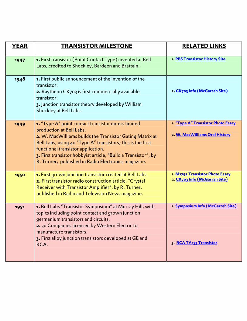
YEAR TRANSISTOR MILESTONE RELATED LINKS
1947 1. First transistor (Point Contact Type) invented at Bell Labs, credited to Shockley, Bardeen and Brattain.
1. PBS Transistor History Site
1948 1. First public announcement of the invention of the transistor. 2. Raytheon CK703 is first commercially available transistor. 3. Junction transistor theory developed by William Shockley at Bell Labs.
2. CK703 Info (McGarrah Site)
1949 1. “Type A” point contact transistor enters limited production at Bell Labs. 2. W. MacWilliams builds the Transistor Gating Matrix at Bell Labs, using 40 “Type A” transistors; this is the first functional transistor application. 3. First transistor hobbyist article, “Build a Transistor”, by R. Turner, published in Radio Electronics magazine.
1. “Type A” Transistor Photo Essay 2. W. MacWilliams Oral History
1950 1. First grown junction transistor created at Bell Labs. 2. First transistor radio construction article, “Crystal Receiver with Transistor Amplifier”, by R. Turner, published in Radio and Television News magazine.
1. M1752 Transistor Photo Essay 2. CK703 Info (McGarrah Site)
1951 1. Bell Labs “Transistor Symposium” at Murray Hill, with topics including point contact and grown junction germanium transistors and circuits. 2. 30 Companies licensed by Western Electric to manufacture transistors. 3. First alloy junction transistors developed at GE and RCA.
1. Symposium Info (McGarrah Site) 3. RCA TA153 Transistor
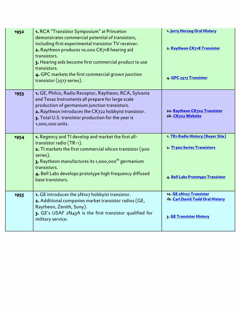
1952 1. RCA “Transistor Symposium” at Princeton demonstrates commercial potential of transistors, including first experimental transistor TV receiver. 2. Raytheon produces 10,000 CK718 hearing aid transistors. 3. Hearing aids become first commercial product to use transistors. 4. GPC markets the first commercial grown junction transistor (2517 series).
1. Jerry Herzog Oral History 2. Raytheon CK718 Transistor 4. GPC 2517 Transistor
1953 1. GE, Philco, Radio Receptor, Raytheon, RCA, Sylvania and Texas Instruments all prepare for large scale production of germanium junction transistors. 2. Raytheon introduces the CK722 hobbyist transistor. 3. Total U.S. transistor production for the year is 1,000,000 units.
2a. Raytheon CK722 Transistor 2b. CK722 Website
1954 1. Regency and TI develop and market the first all-transistor radio (TR-1). 2. TI markets the first commercial silicon transistor (900 series). 3. Raytheon manufactures its 1,000,000th germanium transistors. 4. Bell Labs develops prototype high frequency diffused base transistors.
1. TR1 Radio History (Reyer Site) 2. TI 900 Series Transistors 4. Bell Labs Prototype Transistor
1955 1. GE introduces the 2N107 hobbyist transistor. 2. Additional companies market transistor radios (GE, Raytheon, Zenith, Sony). 3. GE’s USAF 2N43A is the first transistor qualified for military service.
1a. GE 2N107 Transistor 1b. Carl David Todd Oral History 3. GE Transistor History
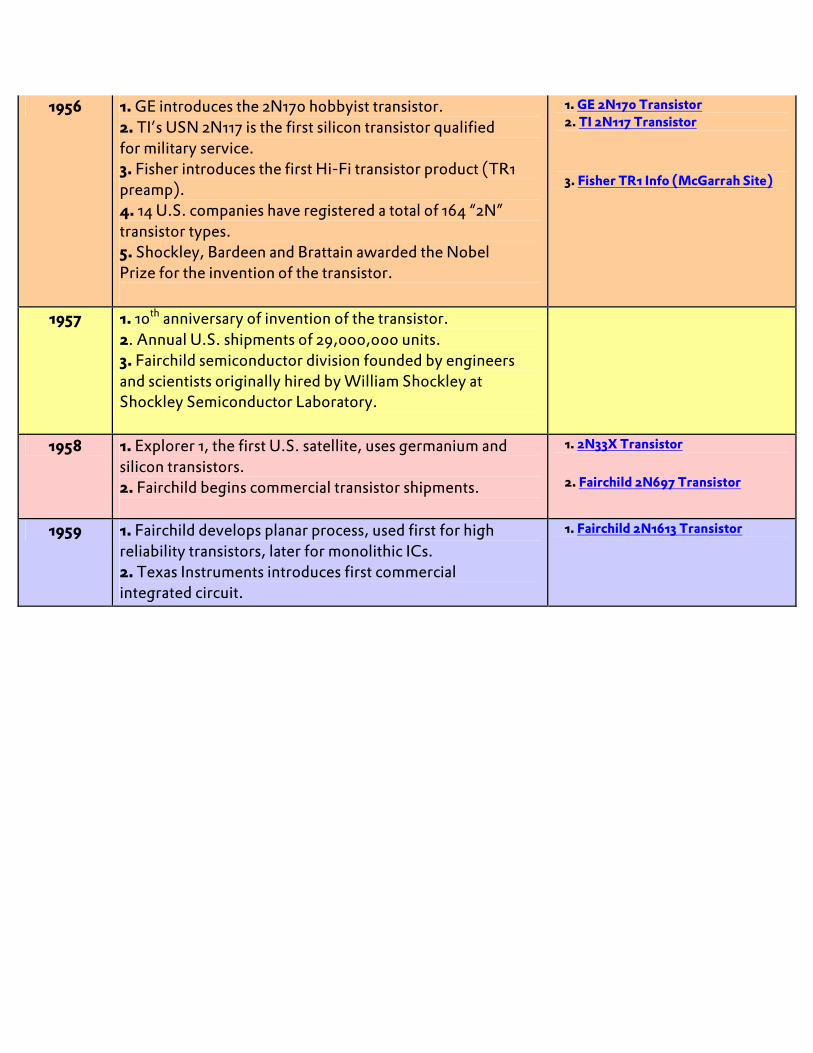
1956 1. GE introduces the 2N170 hobbyist transistor. 2. TI’s USN 2N117 is the first silicon transistor qualified for military service. 3. Fisher introduces the first Hi-Fi transistor product (TR1 preamp). 4. 14 U.S. companies have registered a total of 164 “2N” transistor types. 5. Shockley, Bardeen and Brattain awarded the Nobel Prize for the invention of the transistor.
1. GE 2N170 Transistor 2. TI 2N117 Transistor 3. Fisher TR1 Info (McGarrah Site)
1957 1. 10th anniversary of invention of the transistor. 2. Annual U.S. shipments of 29,000,000 units. 3. Fairchild semiconductor division founded by engineers and scientists originally hired by William Shockley at Shockley Semiconductor Laboratory.
1958 1. Explorer 1, the first U.S. satellite, uses germanium and silicon transistors. 2. Fairchild begins commercial transistor shipments.
1. 2N33X Transistor 2. Fairchild 2N697 Transistor
1959 1. Fairchild develops planar process, used first for high reliability transistors, later for monolithic ICs. 2. Texas Instruments introduces first commercial integrated circuit.
1. Fairchild 2N1613 Transistor
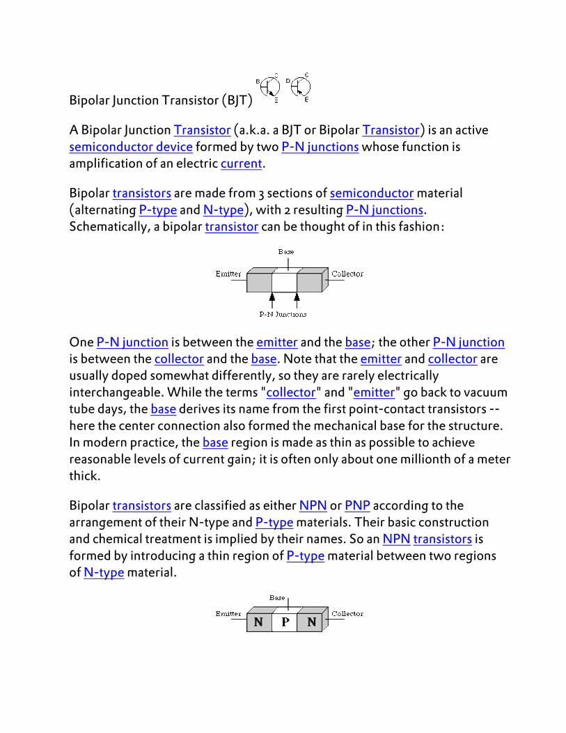
Bipolar Junction Transistor (BJT)
A Bipolar Junction Transistor (a.k.a. a BJT or Bipolar Transistor) is an active semiconductor device formed by two P-N junctions whose function is amplification of an electric current.
Bipolar transistors are made from 3 sections of semiconductor material (alternating P-type and N-type), with 2 resulting P-N junctions. Schematically, a bipolar transistor can be thought of in this fashion:
One P-N junction is between the emitter and the base; the other P-N junction is between the collector and the base. Note that the emitter and collector are usually doped somewhat differently, so they are rarely electrically interchangeable. While the terms "collector" and "emitter" go back to vacuum tube days, the base derives its name from the first point-contact transistors -- here the center connection also formed the mechanical base for the structure. In modern practice, the base region is made as thin as possible to achieve reasonable levels of current gain; it is often only about one millionth of a meter thick.
Bipolar transistors are classified as either NPN or PNP according to the arrangement of their N-type and P-type materials. Their basic construction and chemical treatment is implied by their names. So an NPN transistors is formed by introducing a thin region of P-type material between two regions of N-type material.
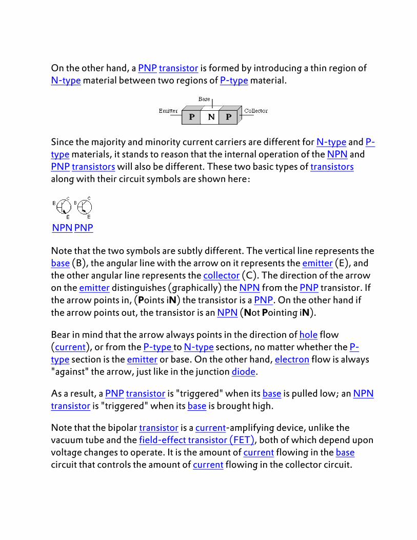
On the other hand, a PNP transistor is formed by introducing a thin region of N-type material between two regions of P-type material.
Since the majority and minority current carriers are different for N-type and P-type materials, it stands to reason that the internal operation of the NPN and PNP transistors will also be different. These two basic types of transistors along with their circuit symbols are shown here:
NPN PNP
Note that the two symbols are subtly different. The vertical line represents the base (B), the angular line with the arrow on it represents the emitter (E), and the other angular line represents the collector (C). The direction of the arrow on the emitter distinguishes (graphically) the NPN from the PNP transistor. If the arrow points in, (Points iN) the transistor is a PNP. On the other hand if the arrow points out, the transistor is an NPN (Not Pointing iN).
Bear in mind that the arrow always points in the direction of hole flow (current), or from the P-type to N-type sections, no matter whether the P-type section is the emitter or base. On the other hand, electron flow is always "against" the arrow, just like in the junction diode.
As a result, a PNP transistor is "triggered" when its base is pulled low; an NPN transistor is "triggered" when its base is brought high.
Note that the bipolar transistor is a current-amplifying device, unlike the vacuum tube and the field-effect transistor (FET), both of which depend upon voltage changes to operate. It is the amount of current flowing in the base circuit that controls the amount of current flowing in the collector circuit.
Wilf Rigter has graciously contributed the following explanation of bipolar transistor behavior in circuits:
You have to think in terms of circuit configurations and the voltage and current in each lead when discussing how transistors behave. There are 3 configurations -- the emitter follower or common collector which is a current amplifier but has no voltage gain, the common emitter amplifier which has current and voltage gain, and the common base amplifier which has voltage gain but no current gain.
1. In an emitter follower circuit with the collector connected to +V and a load connected between the emitter and ground, the voltage applied to the base minus the base emitter forward voltage drop (~0.6 V) will appear across the load (i.e., 5 V base = 4.4 V emitter). The only caveat is that the voltage source at the base must be able to supply about 5% of the load current without appreciable voltage drop. This is a non-inverting voltage follower circuit.
2. In a common emitter circuit with the emitter connected to ground and the load connected between the collector and +V, a voltage connected to the base which exceeds the base emitter forward voltage (0.6V) will rapidly turn on the transistor in proportion to the voltage rise as the base emitter current rapidly increases for a small increase in base voltage. The base voltage source must be able to supply about 5% of the load current into the base emitter diode (i.e., short circuit) for the circuit to develop a large voltage across the load. This is an inverting voltage amplifier circuit.
3. In a common base circuit with the base grounded (or at a reference voltage) and the load connected between the collector and +V, a control voltage connected to the emitter which is more negative than the base emitter forward voltage (~0.6V) causes the transistor to rapidly turn on. The control voltage source must be able to supply about 105% of the load current to develop the full voltage across the
load. This is a non-inverting voltage amplifier circuit.
Review questions
1.Give the expansion of transistor.
2.Give the doping levels of a BJT.
3.Why BJT is called so?
4.Give the three configurations of transistors.
Answers:
1.TRANSfer reSISTOR
2. EMITTER-Heavily Doped, Base-Lightly Doped, Collector- Moderately Doped.
3. BJT is called so, because current conduction is both due to majority and minority carriers .
4.CE,CB & CC.
From the explanation of how a Bipolar Transistor works, we can expect the main characteristic of a Bipolar Transistor to be its Current Gain value. In practice this value isn't a 'universal constant' but depends on various factors: e.g. the transistor's temperature, the size and shape of its Base region, the way it's various parts were doped to make them into semiconductors, etc.
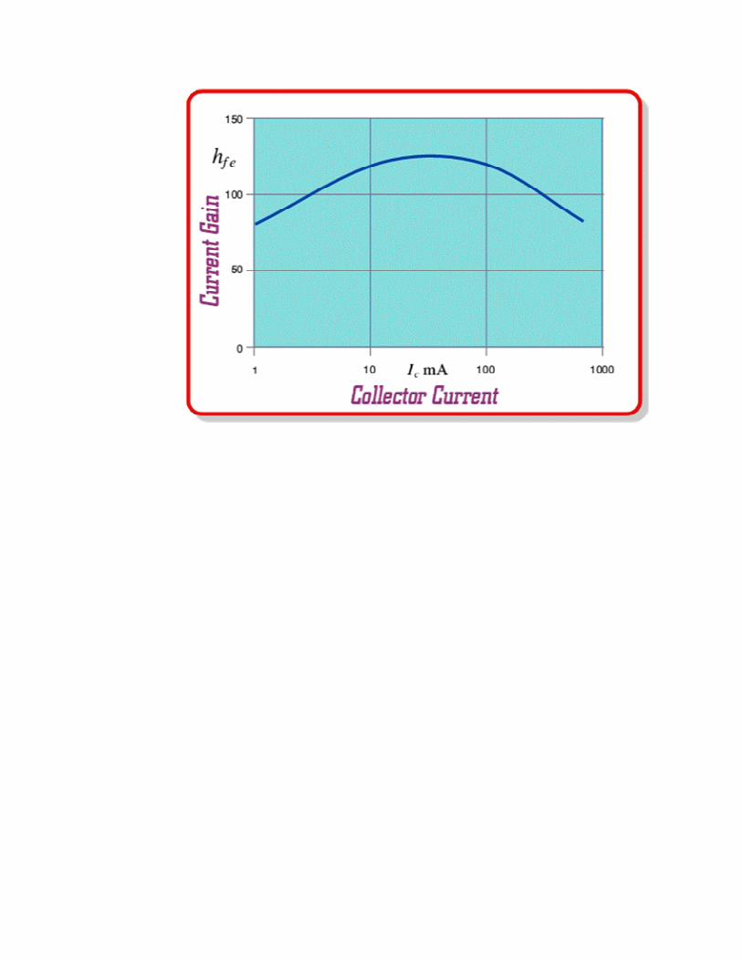
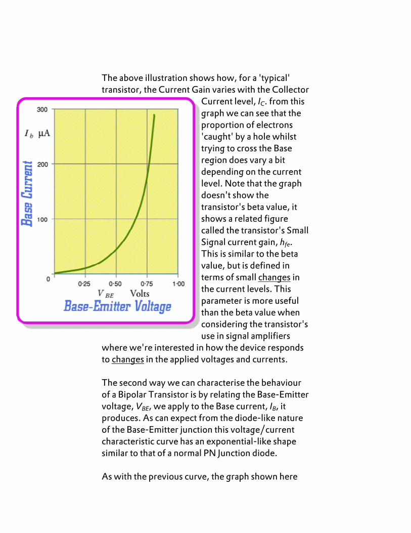
The above illustration shows how, for a 'typical' transistor, the Current Gain varies with the Collector
Current level, IC. from this graph we can see that the proportion of electrons 'caught' by a hole whilst trying to cross the Base region does vary a bit depending on the current level. Note that the graph doesn't show the transistor's beta value, it shows a related figure called the transistor's Small Signal current gain, hfe. This is similar to the beta value, but is defined in terms of small changes in the current levels. This parameter is more useful than the beta value when considering the transistor's use in signal amplifiers
where we're interested in how the device responds to changes in the applied voltages and currents. The second way we can characterise the behaviour of a Bipolar Transistor is by relating the Base-Emitter voltage, VBE, we apply to the Base current, IB, it produces. As can expect from the diode-like nature of the Base-Emitter junction this voltage/current characteristic curve has an exponential-like shape similar to that of a normal PN Junction diode. As with the previous curve, the graph shown here
should only be regarded as a 'typical' example as the precise result will vary a bit from device to device and with the temperature, etc. In most practical situations we can expect the Collector current to be set almost entirely by the chosen Base-Emitter voltage. However, this is only true when the the Base-Collector voltage we are applying is 'big enough' to quickly draw over to the Collector any free electrons which enter the Base region from the Emitter.
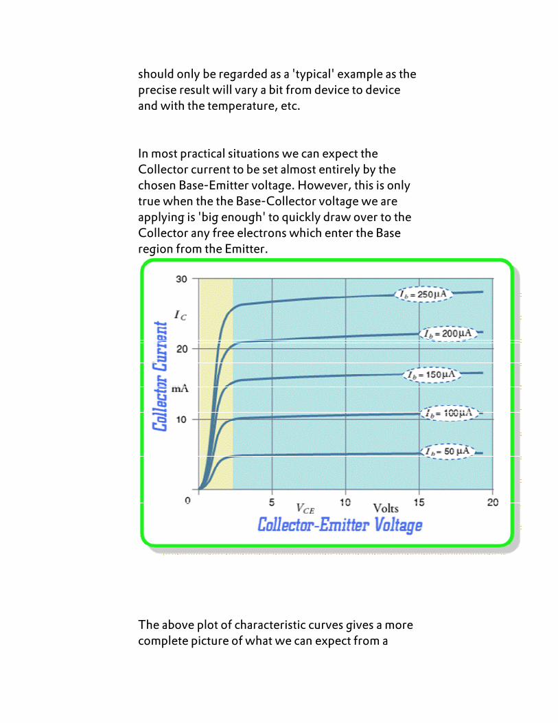
The above plot of characteristic curves gives a more complete picture of what we can expect from a
working Bipolar Transistor. Each curve shows how the colletor current, IC, varies with the Collector-Emitter voltage, VCE, for a specific fixed value of the Base current, IB. This kind of characteristic curve 'family' is one of the most useful ones when it comes to building amplifiers, etc, using Bipolar Transistors as it contains quite a lot of detailed information. When the applied VCE level is 'large enough' (typically above two or three volts, shown as the region in blue) the Collector is able to to remove free electrons from the Base almost as quickly as they Emitter injects them. Hence we get a current which is set by the Base-Emitter voltage and see a current gain value which doesn't alter very much if we change either the base current or the applied Collector potential. However, when we reduce the Collector potential so that VCE is less than a couple of volts, we find that it is no longer able to efficiently remove electrons from the Base. This produces a sort of partial 'roadblock' effect where free electrons tend to hang about in the Base region. (cream coloured region) These makes the Base region seem 'more negative' to any electrons in the Emitter and tends to reduce the overall flow of current through the device. As we lower the Collector potential to become almost the same as that of the Base and Emitter it eventually stops drawing any electrons out of the device and the Collector current falls towards zero. The precise voltage at which the Collector ceases to be an effective 'collector of electrons' depends on the temperature and the manufacturing details of the transisor. In general we can expect most Bipolar Transistors to work efficiently provided that we
arrange for a VCE value of at least two or three volts - and preferrably five volts or more. Such a device can be used as an effective amplifier. Lower voltages may prevent it from working correctly. Note that the graphs shown on this page are only meant as a general guide. Some transistors can work with much higher currents, or have much higher current gains, etc. However, the general pattern of behaviour of all Bipolars is essentially the same as described in these pages. Review questions: 1.Define current gain of CE transistor. 2.How to plot input & output characteristics of transistor configurations? 3.Give some applications of transistors. 4. For more interesting study refer to the following article
How Do Transistors Work?
NO, HOW DO THEY REALLY WORK?
Most introductory textbooks do a very poor job of explaining the details of how transistors work. First they assume that the Base current is somehow controlling the Collector current, then they try to explain how one current can affect another. These explanations always fail because Bipolar transistors, like FETs, are voltage-controlled devices. One current doesn't affect another. Instead, the Base-Emitter voltage controls the thickness of an insulating "depletion layer" which lies in the path of both the Collector current and the Base current.
When I first became interested in electronics as a kid, I sat down and figured out how bipolar transistors work.
Well, sort of.
I read many articles which explained the "Common Base" amplifier. Common-base is the setup which was used by the inventors of the transistor. In those explanations, the Base is grounded and the input signal is applied to the Emitter. Since common-base amplifiers are rarely used in transistor circuitry, I ended up having to dream up my own explanation. I based it upon the little bits I already knew about the Common Emitter configuration. Common Emitter the one where the Emitter is grounded, the Base is the input, and where the output is taken across a resistor connected to the Collector. My home-made explanation sort of worked, but I wasn't satisfied. I was full of niggling doubts. And why the hell were the textbooks using Common Base to introduce transistors to the newbies? It just didn't make any sense.
When I went into engineering school, I found it extremely odd that there were still no good explanations of bipolar transistors. Sure, there were detailed mathematical treatments. Just multiply the Base current by "hfe" to obtain the Collector current. Or, treat the transistor as a
two-port network with a system of equations inside. Ebers-Moll and all that. But these were similar to black-box circuits, and none of them said HOW a transistor works, how can a small current have any effect
on a larger one???? And nobody else seemed curious. Everyone else in the class seemed to think that to memorize the equations was the same as learning concepts and gaining understanding of the device. (R. Feynman calls this the Euclidean or "Greek viewpoint;" the love of mathematics, as opposed to the physicists' " Babylonian viewpoint" where concepts are far more important than equations.) I'm a total Babylonian. For me, math is useless at the start, equations are like those black box Spice programs which might work great, but they don't tell you any details of what's happening inside a device in the real world. Only after I've attained a visual and gut-level understanding of something, only then is the math useful to me for refining it and adding all the details. However, math alone is not a genuine explanation. Math is just a tool or a recipe, a crutch for those who want nothing except the final numerical result, and it certainly does not confer expert knowledge.
Now many years have passed and I think I see the problem...
Traditional transistor explanations basically *suck.* The ones I see in textbooks and hobby magazines are terrible. They're full of errors and contradictions. They misuse the word "current" as if it were a substance that flows. They don't explain insulators properly. And they try to prove that the base current can have an effect on the collector current. And then there's all those authors who use Common-base amplifiers to introduce transistors to newbies. Are they just fools who follow a tradition only because it's traditional? Why don't they ever make efforts to improve the explanations? Were they written in stone by god? Well, if nobody but me thinks the explanation is open to improvements, then I'd better put my money where my mouth is. (And if I'm right, then it should be very easy to write a vastly improved explanation.)
Below are my ideas on how transistors really work. As you'll soon see,

several new concepts are required. It might be easier for you to just memorize the equations rather than to imagine what really goes on inside. But if you DO manage to decode my explanations and crude ASCII artwork, I think you'll be in the elite minority who really
understands transistors. I've found that even most working engineers have no good mental picture of bipolar transistor operation. So, if you attain a clear understanding of transistors, you'll surpass many of the experts.
First of all, you must abandon the idea that current travels in transistors or flows inside of wires. Yes, you heard me right. Current does
not flow. Electric current never flows, since an electric current is not a stuff. Electric current is a flow of something else. (Ask yourself this: what's the stuff that flows in a river, is it "current" or is it called "water?")
So what flows inside of wires?
The stuff that moves within wires is not named Electric Current. Intead it is called Electric Charge. It's the charge that flows, never the current. And in rivers or in plumbing, it's the water that flows, not the "current." We cannot understand plumbing until we stop believing in a stuff called "current," and then we learn that "water" flows inside of pipes. The same is true with circuits. Wires are not full of current, they are full of charges that can move. Electric charge is real stuff; it can move around. But electric current is not stuff. If we decide to ignore "current," and then examine the behavior of moving charges in great detail, we can burn off the clouds of fog that block our understanding of electronics.
Second: the charges found within conductors do not push themselves along, but instead they're pushed by potential difference; they're pushed by the voltage-fields within the conductive material. Charges are not squirted out of the power supply as if the power supply was some sort of water tank. If you imagine that the charges leave through the positive or negative terminal of the power supply; if you think that the charges then spread throughout the hollow pipes of the circuit, then you've
made a fundamental mistake. Wires do not act like "empty electron-pipes," and a power supply does not supply any electrons. Power supplies certainly create currents, or cause currents, but remember, we're removing that word "current." To create a flow of charges, a power supply does not inject any charges into the wires. The power supply is only a pump. A pump can supply a pumping pressure. Pumps never supply the water being pumped.
Third: have you discovered the big 'secret' of visualizing electric circuits?
ALL CONDUCTORS ARE ALREADY FULL OF CHARGE Wires and silicon ...both behave like pre-filled water pipes and water tanks. Electric circuits are based on full pipes. This simple idea is usually obscured by the phrase "power supplies create current," or "current flows in wires." We end up thinking that wires are like hollow pipes, and a mysterious substance called Current is flowing through them. Nope. (Once we get rid of that word "current," we can discover fairly stunning insights into simple circuits, eh?)
If circuits are like plumbing, then none of the
"pipes" of a circuit are ever empty. This idea is extremely important, and without it we cannot understand semiconductors ...or even conductors. Metals contain a vast quantity of movable electrons which forms a sort of "electric fluid" within the metal. A simple block of copper is like a water tank! Physicists call this fluid by the name "electron sea of metals."
Semiconductors are always full of this movable "charge-stuff." The movable charge is there even when a transistor is sitting on the shelf and disconnected from everything. When a voltage is applied across a piece of silicon, those charges already within the material are driven into motion. Also note that the charge within wires is ...uncharged. Every movable electron has a positive proton nearby, so even though the metal contains a vast sea of charge, there is no net charge on average. Wires contain "uncharged" charge. Better call that "cancelled charge." Yet even though the electrons are cancelled by the protons, the electrons can still flow among the protons. Cancelled charge can still move around, so it's possible to have flows of charge in uncharged metal.
OK, since the "pipes" are already full of "liquid," then in order to understand circuitry we should NOT trace out the path starting at the terminals of the power supply. Instead, we can start with any component on the schematic. If a voltage is applied across that component, then the charges within that component will start to flow. Let's modify the old "flashlight explanation" which we all were taught in grade school. Here's the corrected version:
AN ACCURATE FLASHLIGHT EXPLANATION: Wires are full of vast amounts of movable electric charge (all conductors are!) If you connect some wires into a circle, you form an "electric circuit" which contains a movable conveyor-belt made of charges within the
metal. Next we cut this circle in a couple of places and we insert a battery and a light bulb into the cuts. The battery acts as a charge pump, while the light bulb offers friction. The battery pushes the wires' row of charges forward, then all the charges flow, then the bulb lights up. Let's follow them.
The charges start out inside the light bulb filament. (No, not inside the battery. We start at the bulb.) The charges are forced to flow along through the filament. Then they flow out into the first wire and move along to the battery's first terminal. (At the same time more charges enter the filament through its other end.) The battery pumps the charges through itself and back out again. The charges leave the second battery terminal, then they flow through the second wire to the bulb. They wind up back inside the light bulb filament. At the same time, the charges in other parts of the circuit are doing the same thing. It's like a solid belt made out of charges. The battery acts as a drive wheel which moves the belt. The wires behave as if they hide a conveyor belt inside. The light bulb acts like "friction;" getting hot when its own natural charges are forced to flow along. The battery speeds up the entire belt, while the friction of the light bulb slows it down again. And so the belt runs constantly, and the light bulb gets hot.
Brief review:
1. THE STUFF THAT FLOWS THROUGH CONDUCTORS IS CALLED CHARGE. ("CURRENT" DOESN'T FLOW.)
2. THE CHARGE INSIDE CONDUCTORS IS SWEPT ALONG BY VOLTAGE FIELDS.
3. ALL WIRES ARE "PRE-FILLED" WITH A VAST AMOUNT OF MOVABLE CHARGE
4. BATTERIES AND POWER SUPPLIES ARE CHARGE-PUMPS.
5. LIGHT BULBS AND RESISTORS BOTH ACT "FRICTIONALLY."
One more last thing before diving into transistors. Silicon is very different than metal. Metals are full of movable charges... but so is doped silicon. How are they different? Sure, there's that matter of the "band gap," and the difference between electrons versus holes, but that's not the important thing. The important difference is quite simple: metals have vast quantities of movable charge, but silicon does not. For example in copper, every single copper atom donates one movable electron to the "sea of charge." The "electric fluid" is very dense; just as dense as the copper metal. But in doped silicon, only one atom in a billion donates a movable charge. Silicon is like a big empty space with an occasional wandering charge. In silicon, you can sweep all the charges out of the material by using a few volts of potential, while
in a metal it would take billions of volts to accomplish the same thing. Or in other words:
6. THE CHARGE INSIDE OF SEMICONDUCTORS IS LIKE A COMPRESSIBLE GAS, WHILE THE CHARGE INSIDE OF METALS IS LIKE A DENSE AND INCOMPRESSIBLE LIQUID. Sweeping away the charges in a material is the same as converting that material from a conductor to an insulator. If silicon is like a rubber hose, then it's a hose which contains compressible gas. We can easily squeeze it shut and stop the flow. But if copper is also like a rubber hose, then instead, it's like a hose full of iron slugs. You can squeeze and squeeze, but you can't smash them out of the way. But with air hoses and with silicon conductors, even a small sideways pressure can pinch the pathway shut and stop the flow.
.
To turn on an NPN transistor, a voltage is applied across the base and emitter terminals. This causes electrons in the Base wire to move away from the transistor itself and flow out towards the power supply. This in turn pulls electrons out of the P-type base region, leaving 'holes' behind, and the 'holes' act like positive charges which are pushed in the opposite direction from the direction of electron current. What SEEMS to happen is that the base wire injects positive charges into the base region. It
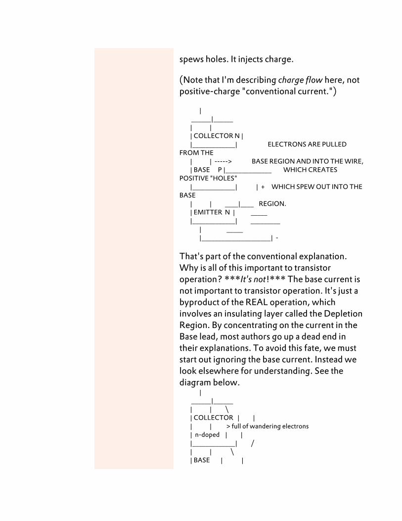
spews holes. It injects charge.
(Note that I'm describing charge flow here, not positive-charge "conventional current.")
| ______|______ | | | COLLECTOR N | |_____________| ELECTRONS ARE PULLED FROM THE | | -----> BASE REGION AND INTO THE WIRE, | BASE P |______________ WHICH CREATES POSITIVE "HOLES" |_____________| | + WHICH SPEW OUT INTO THE BASE | | ____|____ REGION. | EMITTER N | _____ |_____________| _________ | _____ |_____________________| -
That's part of the conventional explanation. Why is all of this important to transistor operation? ***It's not!*** The base current is not important to transistor operation. It's just a byproduct of the REAL operation, which involves an insulating layer called the Depletion Region. By concentrating on the current in the Base lead, most authors go up a dead end in their explanations. To avoid this fate, we must start out ignoring the base current. Instead we look elsewhere for understanding. See the diagram below. | ______|______ | | \ | COLLECTOR | | | | > full of wandering electrons | n-doped | | |_____________| / | | \ | BASE | |
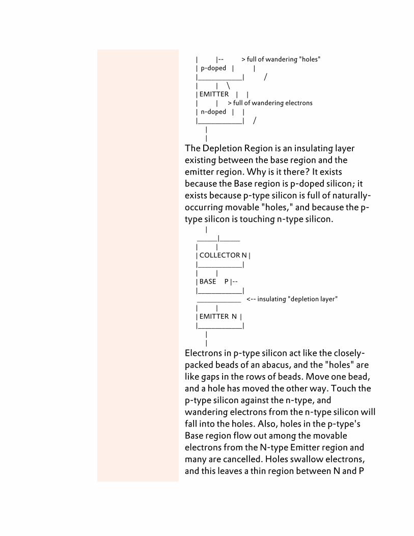
| |-- > full of wandering "holes" | p-doped | | |_____________| / | | \ | EMITTER | | | | > full of wandering electrons | n-doped | | |_____________| / | |
The Depletion Region is an insulating layer existing between the base region and the emitter region. Why is it there? It exists because the Base region is p-doped silicon; it exists because p-type silicon is full of naturally-occurring movable "holes," and because the p-type silicon is touching n-type silicon. | ______|______ | | | COLLECTOR N | |_____________| | | | BASE P |-- |_____________| _____________ <-- insulating "depletion layer" | | | EMITTER N | |_____________| | |
Electrons in p-type silicon act like the closely-packed beads of an abacus, and the "holes" are like gaps in the rows of beads. Move one bead, and a hole has moved the other way. Touch the p-type silicon against the n-type, and wandering electrons from the n-type silicon will fall into the holes. Also, holes in the p-type's Base region flow out among the movable electrons from the N-type Emitter region and many are cancelled. Holes swallow electrons, and this leaves a thin region between N and P
sections which lacks movable charges.
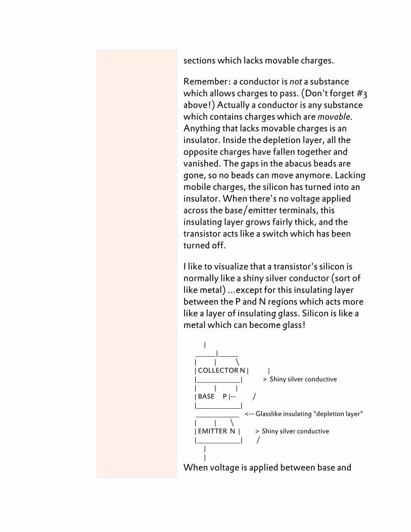
Remember: a conductor is not a substance which allows charges to pass. (Don't forget #3 above!) Actually a conductor is any substance which contains charges which are movable. Anything that lacks movable charges is an insulator. Inside the depletion layer, all the opposite charges have fallen together and vanished. The gaps in the abacus beads are gone, so no beads can move anymore. Lacking mobile charges, the silicon has turned into an insulator. When there's no voltage applied across the base/emitter terminals, this insulating layer grows fairly thick, and the transistor acts like a switch which has been turned off.
I like to visualize that a transistor's silicon is normally like a shiny silver conductor (sort of like metal) ...except for this insulating layer between the P and N regions which acts more like a layer of insulating glass. Silicon is like a metal which can become glass!
| ______|______ | | \ | COLLECTOR N | | |_____________| > Shiny silver conductive | | | | BASE P |-- / |_____________| _____________ <-- Glasslike insulating "depletion layer" | | \ | EMITTER N | > Shiny silver conductive |_____________| / | |
When voltage is applied between base and
emitter, this insulating layer changes thickness.
If (+)voltage is applied to the p-type, to the base wire, while a (-) voltage polarity is applied to the n-type, to the emitter wire, then electrons in the n-type are pushed towards the holes in the p-type. The insulating layer becomes so thin that the clouds of electrons and holes start meeting and combining. A current therefore exists in the base/emitter circuit. But this current is not important to transistor action. What's important to notice is that the *VOLTAGE* across the base/emitter has caused the insulating Depletion Layer to become so thin that the charges can now flow across it. It's as if the transistor contains a layer of glass whose thickness can be varied when we alter a voltage. The layer becomes thinner when base/emitter voltage is increased. This happens because the voltage pushes the holes and the electrons towards each other, reducing the size of the empty insulating region between the clouds of holes and electrons, and allowing the stragglers to jump across the insulator. The depletion layer is a voltage-controlled switch which "closes" when the right polarity of voltage is applied. It is also a proportional switch, since a small voltage can close it only partially. For silicon material, charges start jumping across when the voltage is around 0.3V. Raise the voltage to 0.7V and the current gets very high. (That's for silicon. Other materials have different turn-on voltages.) The larger the voltage, the thinner the insulating layer, so the higher the current in the entire transistor. By applying the right voltage, we can thicken or thin the depletion layer as desired,
Biasing of a transistor The process of applying dc signal to a transistor is known as biasing a transistor.
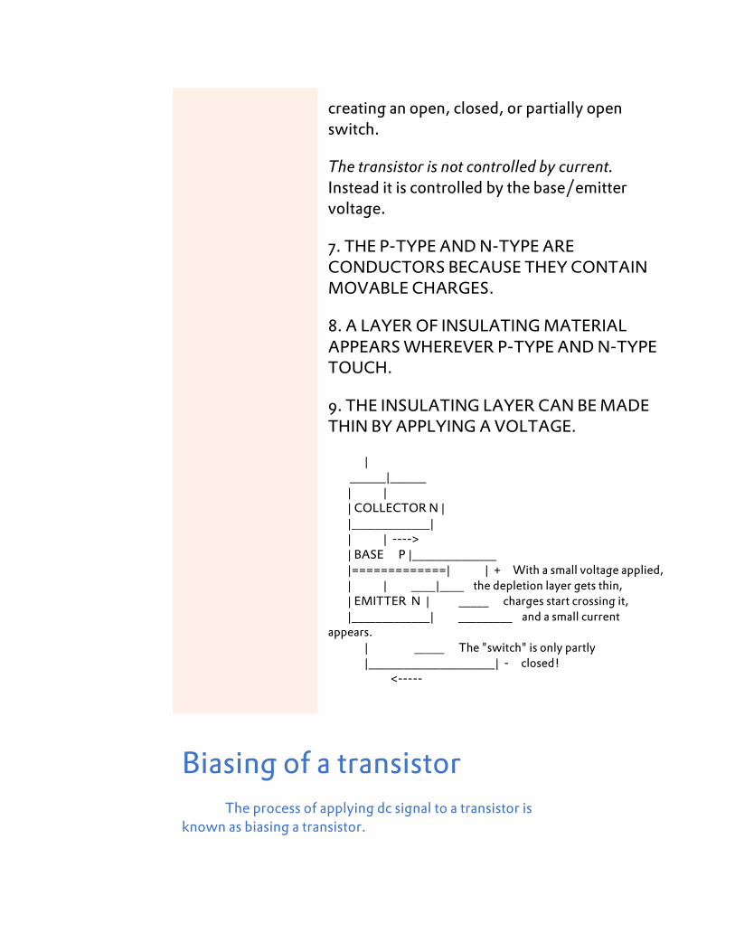
creating an open, closed, or partially open switch.
The transistor is not controlled by current. Instead it is controlled by the base/emitter voltage.
7. THE P-TYPE AND N-TYPE ARE CONDUCTORS BECAUSE THEY CONTAIN MOVABLE CHARGES.
8. A LAYER OF INSULATING MATERIAL APPEARS WHEREVER P-TYPE AND N-TYPE TOUCH.
9. THE INSULATING LAYER CAN BE MADE THIN BY APPLYING A VOLTAGE.
| ______|______ | | | COLLECTOR N | |_____________| | | ----> | BASE P |______________ |=============| | + With a small voltage applied, | | ____|____ the depletion layer gets thin, | EMITTER N | _____ charges start crossing it, |_____________| _________ and a small current appears. | _____ The "switch" is only partly |_____________________| - closed! <-----
For CE Configuration:
In case of using transistor as a ON switch both emitter-base & collector base junctions should be forward biased.
In case of using transistor as an OFF switch both emitter-base & collector base junctions should be reverse biased.
In case of using transistor as an amplifier emitter-base should be forward biased & collector base junctions should be reverse biased.
OPERATING POINT or Q-point
The zero signal values of VCE and IC is known as operating point of a transistor.
To use transistor as a switch
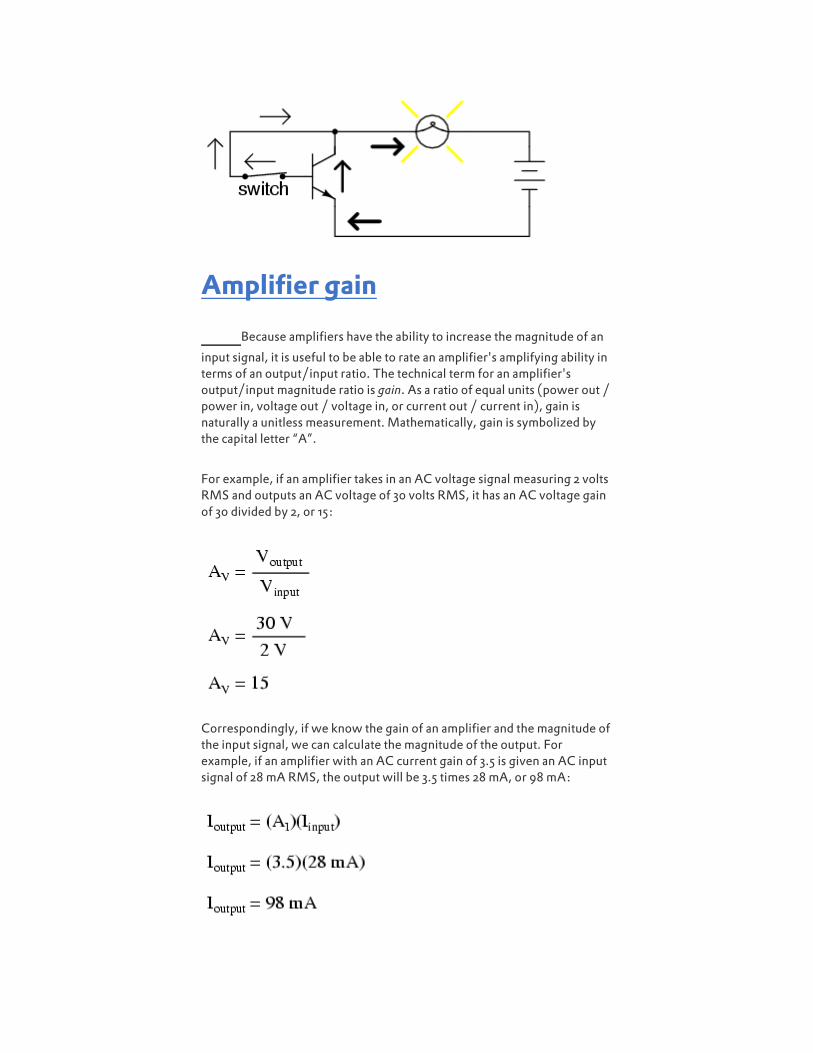
The transistor as a switch
Because a transistor's collector current is proportionally limited by its base current, it can be used as a sort of current-controlled switch. A relatively small flow of electrons sent through the base of the transistor has the ability to exert control over a much larger flow of electrons through the collector.
Suppose we had a lamp that we wanted to turn on and off by means of a switch. Such a circuit would be extremely simple:
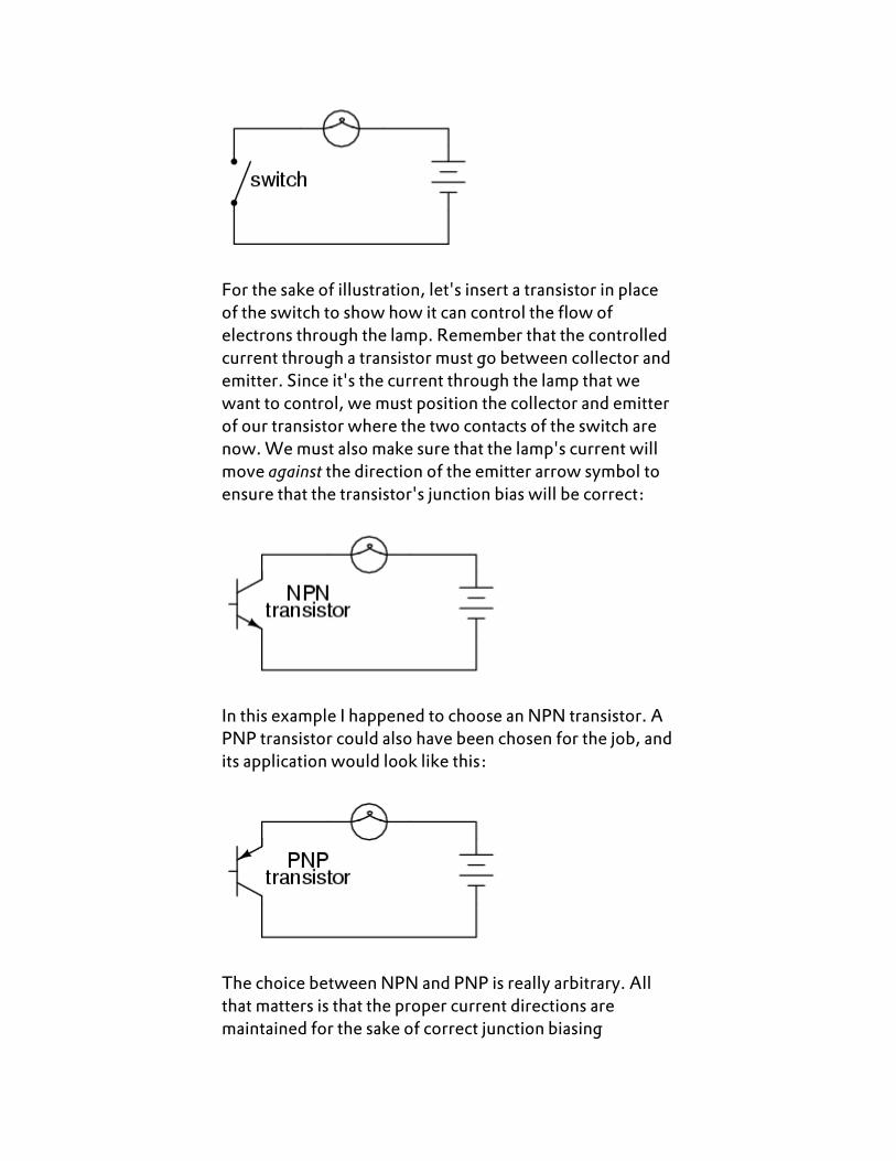
For the sake of illustration, let's insert a transistor in place of the switch to show how it can control the flow of electrons through the lamp. Remember that the controlled current through a transistor must go between collector and emitter. Since it's the current through the lamp that we want to control, we must position the collector and emitter of our transistor where the two contacts of the switch are now. We must also make sure that the lamp's current will move against the direction of the emitter arrow symbol to ensure that the transistor's junction bias will be correct:
In this example I happened to choose an NPN transistor. A PNP transistor could also have been chosen for the job, and its application would look like this:
The choice between NPN and PNP is really arbitrary. All that matters is that the proper current directions are maintained for the sake of correct junction biasing
(electron flow going against the transistor symbol's arrow).
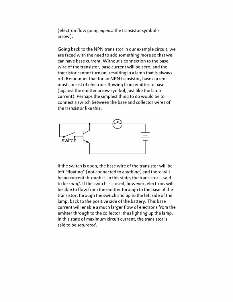
Going back to the NPN transistor in our example circuit, we are faced with the need to add something more so that we can have base current. Without a connection to the base wire of the transistor, base current will be zero, and the transistor cannot turn on, resulting in a lamp that is always off. Remember that for an NPN transistor, base current must consist of electrons flowing from emitter to base (against the emitter arrow symbol, just like the lamp current). Perhaps the simplest thing to do would be to connect a switch between the base and collector wires of the transistor like this:
If the switch is open, the base wire of the transistor will be left "floating" (not connected to anything) and there will be no current through it. In this state, the transistor is said to be cutoff. If the switch is closed, however, electrons will be able to flow from the emitter through to the base of the transistor, through the switch and up to the left side of the lamp, back to the positive side of the battery. This base current will enable a much larger flow of electrons from the emitter through to the collector, thus lighting up the lamp. In this state of maximum circuit current, the transistor is said to be saturated.
Amplifier gain
Because amplifiers have the ability to increase the magnitude of an
input signal, it is useful to be able to rate an amplifier's amplifying ability in terms of an output/input ratio. The technical term for an amplifier's output/input magnitude ratio is gain. As a ratio of equal units (power out / power in, voltage out / voltage in, or current out / current in), gain is naturally a unitless measurement. Mathematically, gain is symbolized by the capital letter “A”.
For example, if an amplifier takes in an AC voltage signal measuring 2 volts RMS and outputs an AC voltage of 30 volts RMS, it has an AC voltage gain of 30 divided by 2, or 15:
Correspondingly, if we know the gain of an amplifier and the magnitude of the input signal, we can calculate the magnitude of the output. For example, if an amplifier with an AC current gain of 3.5 is given an AC input signal of 28 mA RMS, the output will be 3.5 times 28 mA, or 98 mA:
In the last two examples I specifically identified the gains and signal magnitudes in terms of “AC.” This was intentional, and illustrates an important concept: electronic amplifiers often respond differently to AC and DC input signals, and may amplify them to different extents. Another way of saying this is that amplifiers often amplify changes or variations in input signal magnitude (AC) at a different ratio than steady input signal magnitudes (DC). The specific reasons for this are too complex to explain at this time, but the fact of the matter is worth mentioning. If gain calculations are to be carried out, it must first be understood what type of signals and gains are being dealt with, AC or DC.
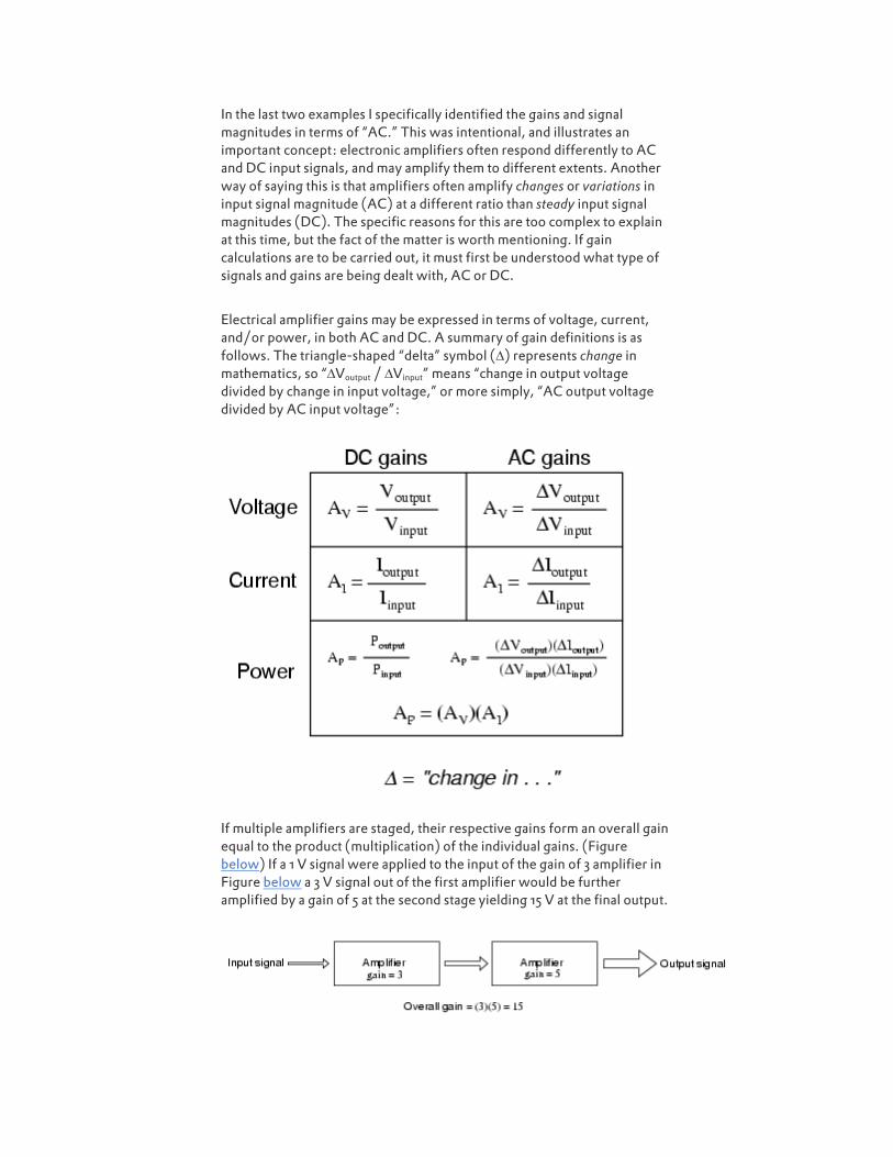
Electrical amplifier gains may be expressed in terms of voltage, current, and/or power, in both AC and DC. A summary of gain definitions is as follows. The triangle-shaped “delta” symbol (∆) represents change in mathematics, so “∆Voutput / ∆Vinput” means “change in output voltage divided by change in input voltage,” or more simply, “AC output voltage divided by AC input voltage”:
If multiple amplifiers are staged, their respective gains form an overall gain equal to the product (multiplication) of the individual gains. (Figure below) If a 1 V signal were applied to the input of the gain of 3 amplifier in Figure below a 3 V signal out of the first amplifier would be further amplified by a gain of 5 at the second stage yielding 15 V at the final output.
The gain of a chain of cascaded amplifiers is the product of the individual
gains.
In electronics, a common-emitter amplifier is one of three basic single-stage bipolar-junction-transistor (BJT) amplifier topologies, typically used as a voltage amplifier. In this circuit the base terminal of the transistor serves as the input, the collector is the output, and the emitter is common to both, hence its name. An analogous circuit called the common source is constructed using field-effect transistors.
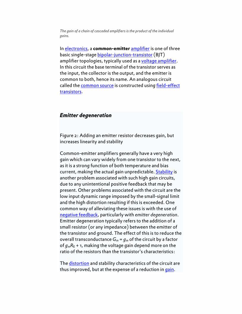
Emitter degeneration
Figure 2: Adding an emitter resistor decreases gain, but increases linearity and stability
Common-emitter amplifiers generally have a very high gain which can vary widely from one transistor to the next, as it is a strong function of both temperature and bias current, making the actual gain unpredictable. Stability is another problem associated with such high gain circuits, due to any unintentional positive feedback that may be present. Other problems associated with the circuit are the low input dynamic range imposed by the small-signal limit and the high distortion resulting if this is exceeded. One common way of alleviating these issues is with the use of negative feedback, particularly with emitter degeneration. Emitter degeneration typically refers to the addition of a small resistor (or any impedance) between the emitter of the transistor and ground. The effect of this is to reduce the overall transconductance Gm = gm of the circuit by a factor of gmRE + 1, making the voltage gain depend more on the ratio of the resistors than the transistor's characteristics:
The distortion and stability characteristics of the circuit are thus improved, but at the expense of a reduction in gain.
Applications
Radio
Common-emitter circuits are used to amplify weak voltage signals, such as the faint radio signals detected by an antenna. When used in radio frequency circuits, it is common to replace the load resistor with a tuned circuit. This is done to limit the bandwidth to a narrow band centered around the intended operating frequency. More importantly it also allows the circuit to operate at higher frequencies as the tuned circuit can be used to resonate any inter-electrode and stray capacitances, which normally limit the frequency response. Common emitters are also commonly used as low noise amplifiers.
Bandwidth
The bandwidth of the common emitter amplifier tends to be low, due to high capacitance resulting from the Miller effect. The base-collector capacitance is effectively multiplied by the factor 1 − Av, thus increasing the total input capacitance and lowering the overall bandwidth. The discussion of bandwidth parallels that in the article on the common source amplifier. A fix for this bandwidth problem is the cascode amplifier.
Stabilizing an amplifier
The invention generally relates to stabilizing an amplifier. In one aspect, a stabilization module that is in electrical communication with the amplifier is provided. The stabilization module includes both an open loop control system and a closed loop control system. The open loop control system is used to modify at least one characteristic of an input signal received by the stabilization module and to pass control to the closed loop control system. The closed loop control system is then used to modify the at least one characteristic of the input signal. The modified input signal is provided to the amplifier.