Embed Size (px)
Citation preview

UNIT-II
Transistor Characteristics - Biasing and Thermal Stabilization: The Junction Transistor, Transistor Current
Components, The Transistor as an Amplifier, Transistor Construction, Detailed study of the Currents in a
Transistor, The Transistor Alpha. The Common-Base Configuration, The Common-Emitter Configuration, The
Common-Collector Configuration. The Ebers-Moll model, The operating point, Analysis of Fixed Bias,
Collector-to-Base bias, Emitter–Feedback bias, Collector-Emitter feedback bias and Self—bias circuits, Stability
factor, Bias compensation techniques, Bias Compensation, Thermal Runaway, Thermal Stability.
INTRODUCTION
A bipolar junction transistor (BJT) is a three terminal device in which operation depends on the interaction of
both majority and minority carriers and hence the name bipolar. The BJT is analogues to vacuum triode and is
comparatively smaller in size. It is used as amplifier and oscillator circuits, and as a switch in digital circuits. It
has wide applications in computers, satellites and other modern communication systems.
BJT AND ITS SYMBOLS
The Bipolar Transistor basic construction consists of two PN-junctions producing three connecting terminals
with each terminal being given a name to identify it from the other two. These three terminals are known
and labelled as the Emitter ( E ), the Base ( B ) and the Collector ( C ) respectively. There are two basic
types of bipolar transistor construction, PNP and NPN, which basically describes the physical arrangement
of the P-type and N-type semiconductor materials from which they are made.
Transistors are three terminal active devices made from different semiconductor materials that can act as either
an insulator or a conductor by the application of a small signal voltage. The transistor's ability to change between
these two states enables it to have two basic functions: "switching" (digital electronics) or "amplification"
(analogue electronics). Then bipolar transistors have the ability to operate within three different regions:
1. Active Region - the transistor operates as an amplifier and Ic = β.Ib
2. Saturation - the transistor is "fully-ON" operating as a switch and Ic = I(saturation)
3. Cut-off - the transistor is "fully-OFF" operating as a switch and Ic = 0
Bipolar Transistors are current regulating devices that control the amount of current flowing through them in
proportion to the amount of biasing voltage applied to their base terminal acting like a current-controlled switch.
The principle of operation of the two transistor types PNP and NPN, is exactly the same the only difference being
in their biasing and the polarity of the power supply for each type(fig 1).

The construction and circuit symbols for both the PNP and NPN bipolar transistor are given above with the arrow
in the circuit symbol always showing the direction of "conventional current flow" between the base terminal and
its emitter terminal. The direction of the arrow always points from the positive P-type region to the negative N-
type region for both transistor types, exactly the same as for the standard diode symbol.


TRANSISTOR CURRENT COMPONENTS:
Fig 3.2 Bipolar Junction Transistor Current Components
The above fig 3.2 shows the various current components, which flow across the forward biased emitter junction
and reverse- biased collector junction. The emitter current IE consists of hole current IPE (holes crossing from
emitter into base) and electron current INe (electrons crossing from base into emitter).The ratio of hole to
electron currents, IpE /InE , crossing the emitter junction is proportional to the ratio of the conductivity of the p

material to that of the n material. In a transistor, the doping of that of the emitter is made much larger than the
doping of the base. This feature ensures (in p-n-p transistor) that the emitter current consists an almost entirely
of holes. Such a situation is desired since the current which results from electrons crossing the emitter
junction from base to emitter do not contribute carriers, which can reach the collector.
Not all the holes crossing the emitter junction JE reach the the collector junction JC Because some of them combine
with the electrons in n-type base. If IpC is hole current at junction JC there must be a bulk recombination current
( IPE-IpC ) leaving the base.
Actually, electrons enter the base region through the base lead to supply those charges, which have been lost by
recombination with the holes injected in to the base across JE. If the emitter were open circuited so that IE=0
then IpC would be zero. Under these circumstances, the base and collector current IC would equal the reverse
saturation current ICO. If IE≠0 then
IC= ICO- IpC
For a p-n-p transistor, ICO consists of holes moving across JC from left to right (base to collector) and
electrons crossing JC in opposite direction. Assumed referenced direction for ICO i.e. from right to left, then for a
p-n-p transistor, ICO is negative. For an n-p-n transistor, ICO is positive. The basic operation will be described
using the pnp transistor. The operation of the pnp transistor is exactly the same if the roles played by the
electron and hole are interchanged. One p-n junction of a transistor is reverse-biased, whereas the other is forward-
biased.
Emitter Injunction Efficiency ( ): It is the ratio of the current through the emitter junction due to the carrier of
the emitter and the total current through the emitter junction.
Base Transport Factor
It is the ratio of hole current through collector junction and hole current through emitter junction.
Reverse Saturation Current (ICO): Due to the reverse voltage , the reverse saturation current also flows
through collector junction.

Bipolar Transistor Configurations
As the Bipolar Transistor is a three terminal device, there are basically three possible ways to connect
it within an electronic circuit with one terminal being common to both the input and output. Eac h
method of connection responding differently to its input signal within a circuit as the static
characteristics of the transistor vary with each circuit arrangement.
1. Common Base Configuration - has Voltage Gain but no Current Gain.
2 Common Emitter Configuration - has both Current and Voltage Gain.
3. Common Collector Configuration - has Current Gain but no Voltage Gain.
COMMON-BASE CONFIGURATION
Common-base terminology is derived from the fact that the base is common to both input and output of
configuration. base is usually the terminal closest to or at ground potential. Majority carriers can cross the reverse-
biased junction because the injected majority carriers will appear as minority carriers in the n-type material. All
current directions will refer to conventional (hole) flow and the arrows in all electronic symbols have a direction
defined by this convention.
Note that the applied biasing (voltage sources) are such as to establish current in the direction indicated for each
branch.
To describe the behavior of common-base amplifiers requires two set of characteristics:
1. Input or driving point characteristics.
2. Output or collector characteristics

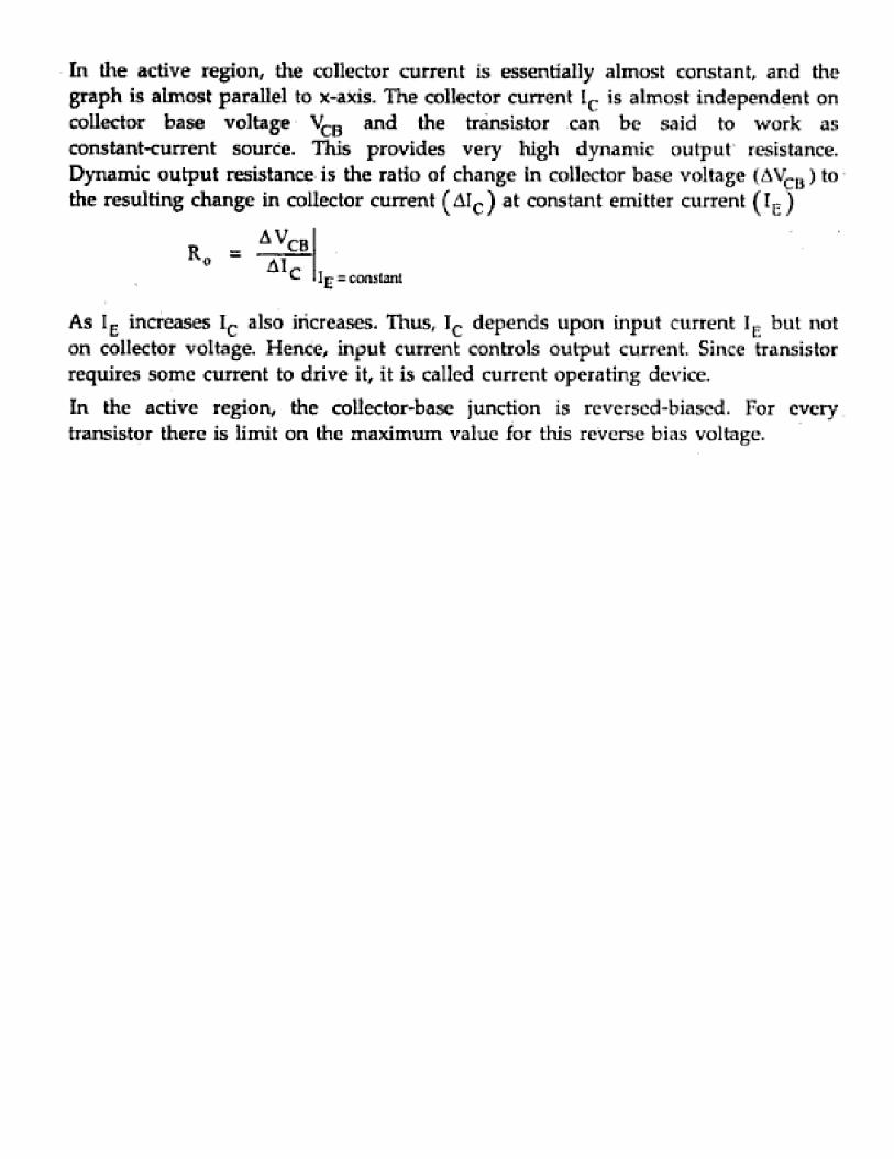
The output characteristics has 3 basic regions:
Active region –defined by the biasing arrangements
Cutoff region – region where the collector current is 0A
Saturation region- region of the characteristics to the left of VCB = 0V