Embed Size (px)
Citation preview

111111 1111111111111111111111111111111111111111111111111111111111111111111111111111us 20120274596Al
(19) United States(12) Patent Application Publication
LUDWIG(10) Pub. No.: US 2012/0274596 Al(43) Pub. Date: Nov. 1,2012
(54) USE OF ORGANIC LIGHT EMITTING DIODE(OLED) DISPLAYS AS A HIGH-RESOLUTIONOPTICAL TACTILE SENSOR FOR HIGHDIMENSIONAL TOUCHPAD (HDTP) USERINTERFACES
(76) Inventor:
(21) Appl. No.:
(22) Filed:
Lester F. LUDWIG, Belmont, CA(US)
13/547,024
Jul. 11, 2012
Related U.S. Application Data
(60) Provisional application No. 61/506,634, filed on Jul.11,2011.
Publication Classification
(51) Int. CI.G06F 3/041 (2006.01)G09G 3/30 (2006.01)
(52) U.S. CI. 345/173; 345/76
(57) ABSTRACT
A finger-operated touch interface system is physically asso-ciated with a visual display. The system includes a processorexecuting a software algorithm and an array of transparentorganic light emitting diodes (OLEDs) communicating withthe processor. The system operates a group ofOLEDS fromthe OLED array in light sensing mode. These OLEDs detectlight via photoelectric effect and communicate light detectionmeasurements to the processor. The software algorithm pro-duces tactile measurement information responsive to lightreflected by a finger proximate to the OLED array, andreflected light is received by at least one OLED in the trans-parent OLED array and originates from a software-controlledlight source. In one approach, the reflected light is modulatedand the system is responsive to reflected modulated light. Theprocessor generates a control signal responsive to thereflected light. The system can be used to implement anoptical touchscreen without an RF capacitive matrix.

Patent Application Publication Nov. 1,2012 Sheet 1 of 46 US 2012/0274596 Al
~.3:(:t:~h~$.~n$f:.r·rrl::t':!<y {~n~lyht~
~;:~j.;J~~(;~%:i~:?;{~rnnay~)JlJ:-,:·;h!,:).:r:;~:;::i:<
QQOO\\._ C:> .)
ta:;~~h:;:::(Z:aS':}Fw:x::ry (;:R:ry h·.;:
~l H;:H:(:}~:;:.::;t»:tr~:?
t:y.:;ts.k: :~':~f~;:;.{;:r;:;I1nfY
mud),$,:mml
mray (rr~::ryb:t..:;;~ ~:.w:;.;J~~{:;:'::::-·(:~::)
figure ttl
t:jit$.h~ :::~:'fS:,*'$f ;jJ;Y~;;.;:
H}lK:hs;,;::rex~~
tl<.'i.ik ,;",~:~:;ra::t::::-y{!:u:;~ybe
t~·!t~d~;:;;(::tX:::::l:'i~
~;~~;t~~::::$*~~»:.(rmn:;? kiti:.~r<)f tN.)ill
t's»:y t-.-i::;~ ~~)t:::d(S(:{~:i:n)

Patent Application Publication Nov. 1,2012 Sheet 2 of 46 US 2012/0274596 Al
----_.,.::,-.,.,~"
.: ,401b, .. ..,{,
41.i5:a 4Moa / J¥j~h,*~B..../

Patent Application Publication
'U*dik~:';'~i~':i$,H
/ ...n·~ry-;-I);:;,,,
Nov. 1,2012 Sheet 3 of 46
hm;g~ I~H}~>';;~?i~,i!lgD_,r }~:m:::H~'t:'!;Rat~\
,mri Sym1:i{)l Pmri!.lNi;;w\
\
~......•.. ,L•... "1/' !/
j'w;:)·/I'e'tmsnal Pm:$.'>l!f~A!«~r;~.sngE'.km·::::r,t,",,,,,,,,,,,,,,,,,,,,,,,,,,,,,,,,,,,,,,,,,,,,,,,,,,,,,,,,,,,,,,,,,,,,,,,,,,,,,,,,,,,,,,,,,,,,,,,,,,,,,,,,,,,,,,,,,,,,,,,,,,,,,,,,,,,,,,,,,,,,,,,,,,,,,,,,,,,,,,,,"'''''''''''''''''''''''''''''''''''''''''''''''''''''''''''''''''''''''''''''''''''''''''''''''''''''''''''''''''''''''''
US 2012/0274596 Al
r------,I\lnml-CNr
-- PRIOR ART .~
~~.;:~~~:~~ti:nZ:t~t~ __ "':::::........_._..1
1
·················· ·1 ~igmll S')W<::<:'! ...
\.:.
Patent Application Publication Nov. 1,2012 Sheet 4 of 46 US 2012/0274596 Al

Patent Application Publication Nov. 1,2012 Sheet 5 of 46 US 2012/0274596 Al
....,..! I, •••••• , •.••. " ••••. .< •• L...! -==- ~.>"\ .:-:':::.:.:.:.:.:.:.:.::::~. ..:.. :••••:»»:,.
~::::::::::.::;::j/]. : It(: ,/
-I~RIORART-
/r···.L:~::;;;:·~~:L······ll(:· ", /
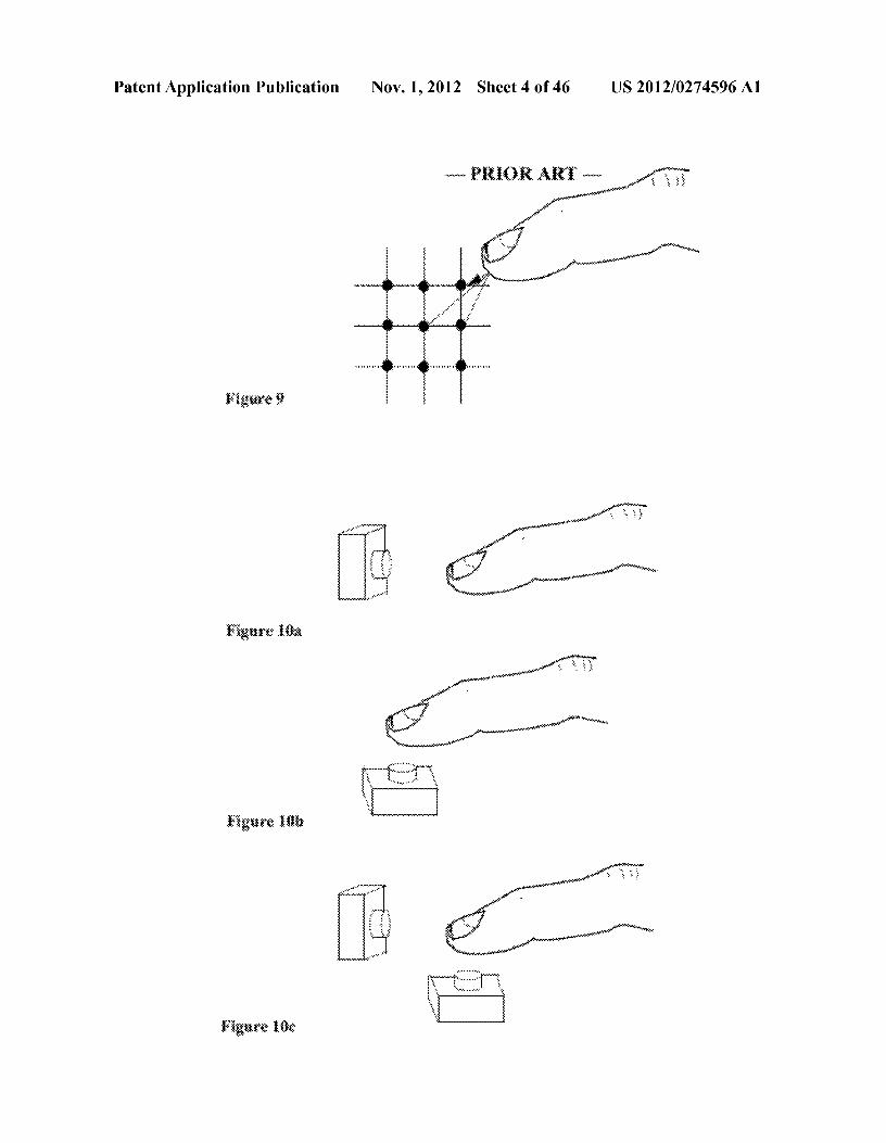
Patent Application Publication Nov. 1,2012 Sheet 6 of 46 US 2012/0274596 Al
1""·····r·····T······T·····T······T·····T······T······T······r······T·····T·····]~ !f...................................... .. ".
; 1
-------+---:

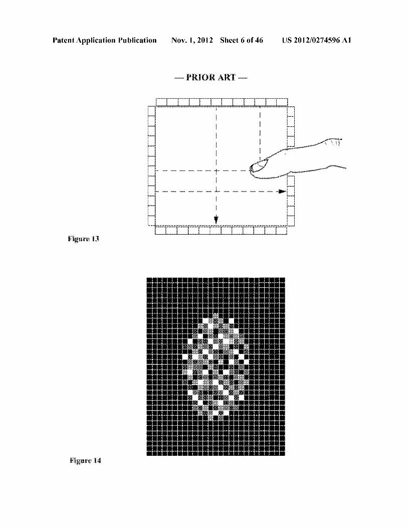
Patent Application Publication Nov. 1,2012 Sheet 7 of 46
r------,Stlu;.;!tm::J
i\.1~'~l.$UB;~nl(1~!.
US 2012/0274596 Al
! Emj)nk;:~ly.r--- ........l fkt¢ImilWil
TPf.;);;~:*":?(:~!;1. !
1hcHk:::k(!:~.<r
c:::::::::::::::::::::>
o
·;·:R~w:"\IC<l:;:;l.lt~.::mCI~t;;lMil.:j;.i:n~ilm
l"'ii.::~@Wie>;l·.·t.~ll·:>.arO}m~y;ln,,:a!ims ..
{l'm:i;!:xitm:pk :;:(:itk and llflkf "(\m!p(:!,~i:;H¢<f'M~~~\$nl,:m·mll-d<d~:~~stf~:&~B
.......I'RIOR AR'r .

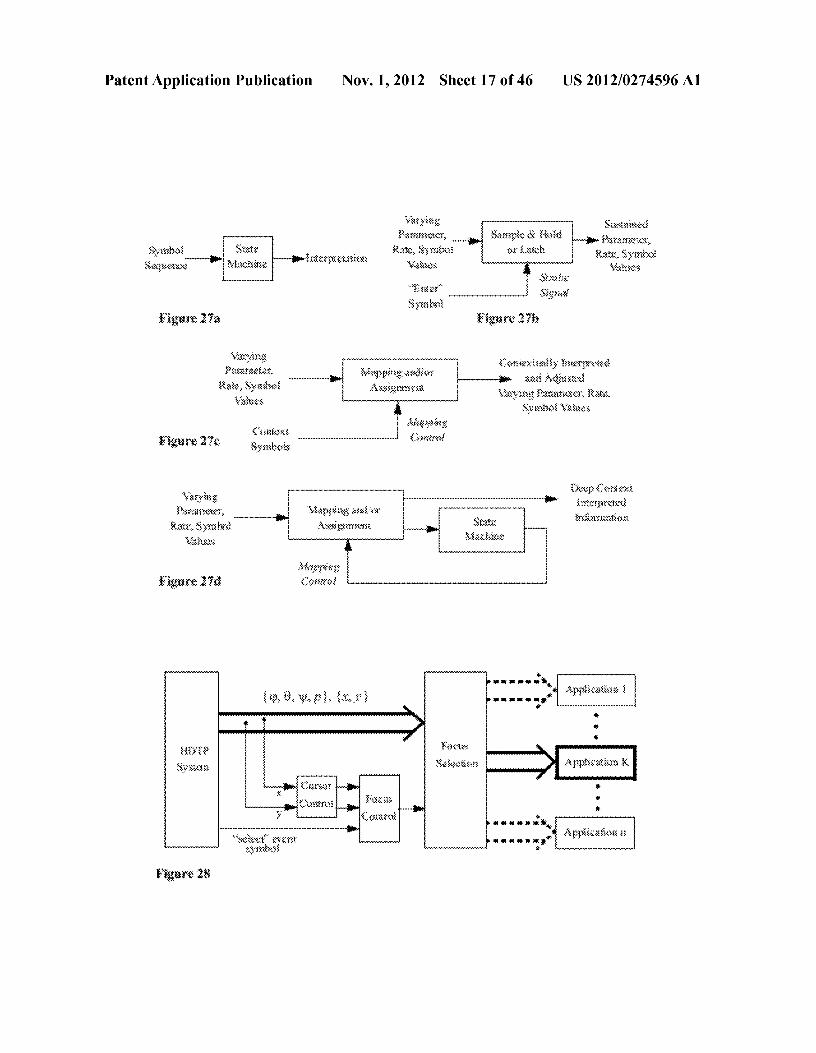
Patent Application Publication Nov. 1,2012 Sheet 8 of 46 US 2012/0274596 Al
~..,...~.., ,., ..'
( ~ """" .
..........
( . l...'.'.'.'.;._ :., ;)( , : :.:•.•.............
L:.>.,..~i',.;,..t. <.~i;"·'i',,···'·'·,,'l..··l··· ..·..·~-!".".~<;, ......... ~ t "'';''.~ {:: J::" ~.' .'_
:;( ..'
//·Z·····/.· ..········..····················.·.·.·.·.·.· ~O';":'f'i/ f~"""o/'A·-....-'-~ . ,..,
// . (5/' _.-~./ ....__.-'" /
~./............_ _ ~ ,.,.,.,.: i'
./ . ....;.;:::.:;:.:.;.::.;;_;;»"'1"\t"
tdo/' ." -r">../ )'~ ....~~;:
'.
' !
.•./<.•..............- ~ ,.,.,.,.:._ .

Patent Application Publication Nov. 1,2012 Sheet 9 of 46 US 2012/0274596 Al
I!k~!h!m" '-''i'w!:!!;.lJ!!W,n~Hi3clll
m¢ibmt'~lx;:;~!d .-i \,.;"!\"··,·C~iV
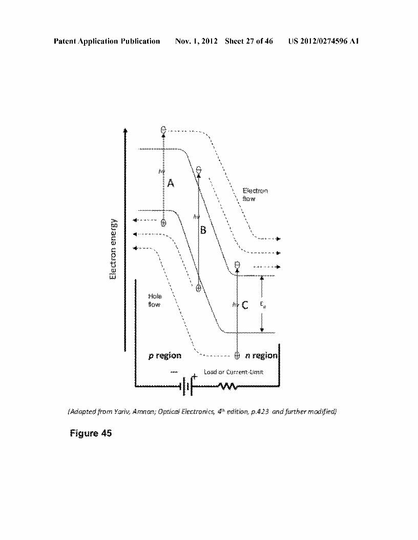
'~zmdsum,:spf<:3.d
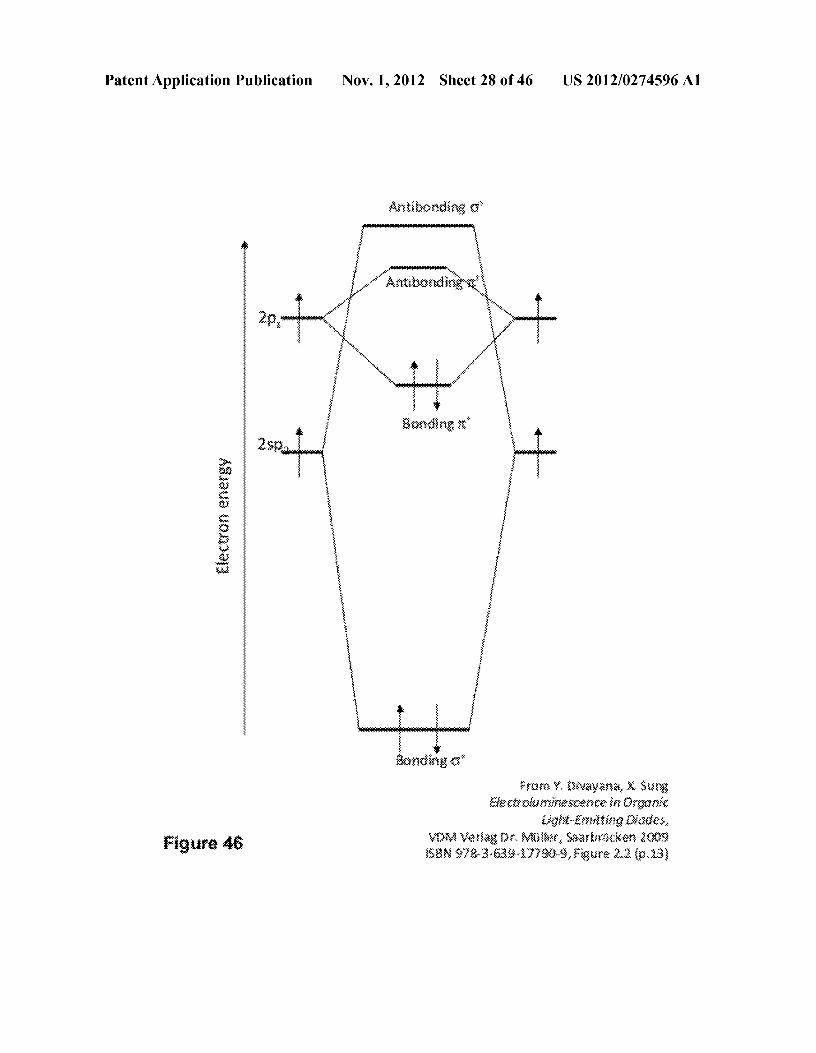
y:,:.w':..CC\V
'7~~)j1:r/( •.•......" ~./ w ._..•..c
:br·;:!pr!:!!>:1p:iidH~~~tlmli
:(l::r,,::;pi:<~lldr:~i:d!·w
r H):g~th<=:f''y2)S'" nl:;\ltra!
ll}g~llwrYllW"C,\V
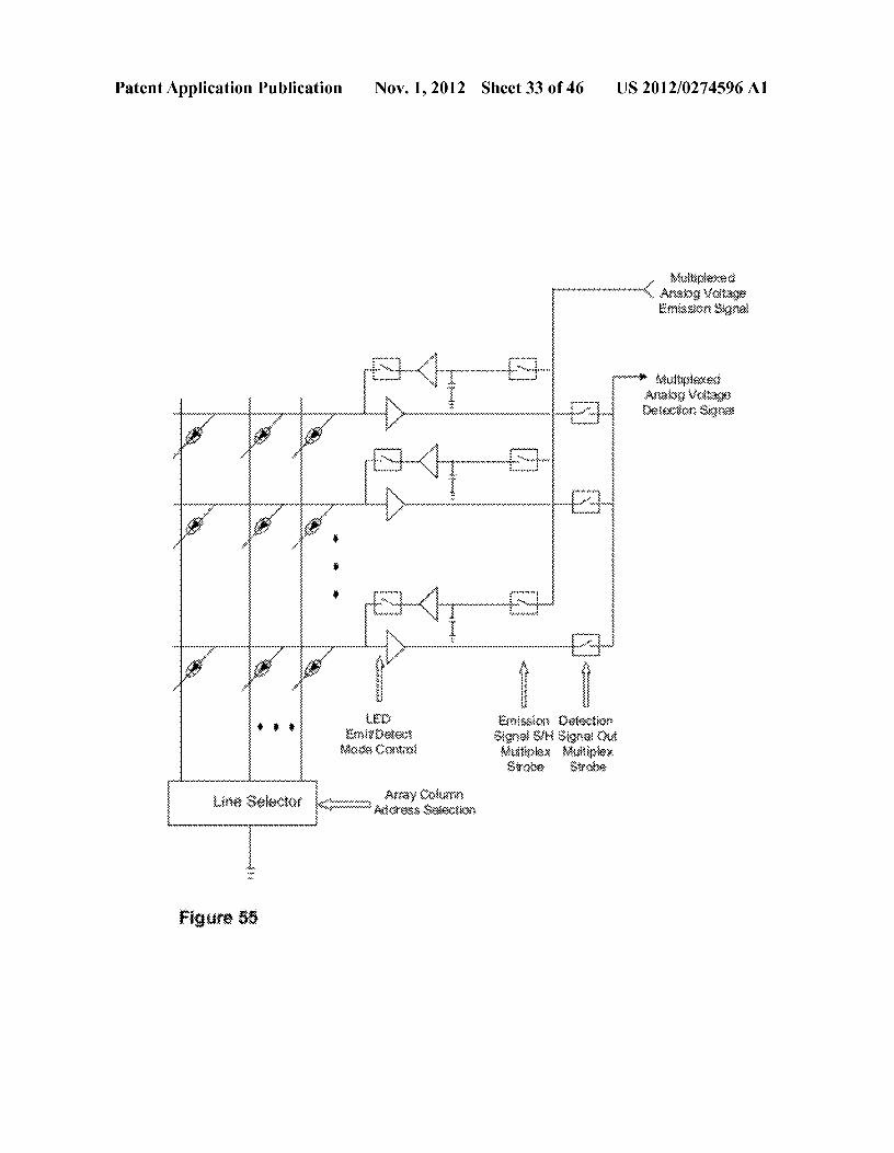
.:...-._._ .....,., •....................................•
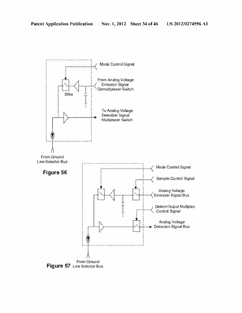
~~iln
ti;'2:~x:thi:'t')"M····(:c'\",../ \.. /.- ,.,
;:.
.::.:.:;•..l..:..~ ~::..2.,..: ".••.~: :.:;.:•.::::.:•..•.0•.•.~::..•,~;.:::'.'::~::.:~:/.::..:..';..:.,•..••:.:.:/.::.:,:.:)•...~ :.~..i/···~·~·:..A~~?:)::\.:;".c~b" ,- J' . /' ~~:~~~~~.r(}«>
ll:'l?'!:ll:,;:r pi!;.:lJ,··!.lj> h~~3.tk:rrird"":!l~'!li:«IJ

Patent Application Publication
1.~. Pt~l$..""~~l:;
...................../'t <,
........
lOll\,t.;jhdaH;:IHdFist
2tHlb
:UHle \, /........~. ,/
........... ..; ..
Nov. 1,2012 Sheet 10 of 46 US 2012/0274596 Al
2001 Thumb/\../ \.~~
:.
(l002
- ir;:r:ers.egm.;::nt
liHlWholeH~:~ndFlat$pre.adFingers
2fHJd\:'~), ••••••, •.._.;.•••w .•' -,

Patent Application Publication
{~}!~d~;;;.::ij);:d~~;f(:~~~~
:~:r:::r::.::g~:~~n::;~;:.f>.?:h;;::r:::: ~':{::::S:SUf;~~
M r)";::Kimity·<:>;N:';;:&;··:::·<hi';):'li{,~m
II
~J$asur(;":i:lPl't%:nrt~<)rpr(}~imity hl1{lgi.~
Nov. 1,2012 Sheet 11 of 46 US 2012/0274596 Al
P'il1ger "A"{hrrlwd}
fY1lrpw -s:(t/:at.)
- -- -- --.!M!' i!w:!:,:;;:~!i!:i:>l
····lliAd· .....
UPIWTPalm
Impliedfhmd l\)S1Uf«

Patent Application Publication
'$) ,,,_,J!i~._----------- -----------
1
:z ':>':
.~-r-, :,;...,.~ ~~ <:;s :$)-
(~ § ::::;.<-:.
'+'-l- ~~:.~ ~ £:::"'~ ,"> ':::::.,....... ::::; .~.8- ::::;: -:::-:..a ;~.
2 ...~ _.:':;;:':18 :~ :;::;.
~ :;;:;.".".;
I ~ 1r
Nov. 1,2012 Sheet 12 of 46 US 2012/0274596 Al
•.•.•.•.y.•.•.•.•.•.•.•.•.•.•.•.•.
:jg!~;:::
~
Ii*
"X ~J'~a~ :::;;;t::m.~~,:~ .~'~
a~§,·~..................y .

Patent Application Publication
r J __ '1
Hklb Sh~~p"R.;$ii:DW~·~ti~:}n
L
Nov. 1,2012 Sheet 13 of 46
1
gt~ptitat¢hl~~3gZ;;s
.1/ !!!!!!!!!!!!!..
\
US 2012/0274596 Al
C:nmpfHwdlnti@t:$
'.
........
-c~ -,
r--~·---!BVAJ C\m:Mm.Mk~n/
/\:%t~d:';im RtKT~gnh.innL,~_,_! .J
r·'· ...,..,. ..,..,... ,..,... ,..,.•. ,..,..,. "1
! PRn:j.m::;;%~r),laPIJing: lL----r----~

Patent Application Publication Nov. 1,2012 Sheet 14 of 46 US 2012/0274596 Al
F.nHne::xo.FRiZfbmn:(.~eC:nthN.'thm.
Rl:u~g$·:{tF:RotaHQnC:nrrt'd.~nn
td¢t~:j·I'h(lf'B1~$:t:dCnrrt'rh{:;4~

Patent Application Publication
Figure 24h
Nov. 1,2012 Sheet 15 of 46 US 2012/0274596 Al
~x';}vnm n},v~;t:nkr of :::~nt<..";ofp:n::::i.:Hlt\~ pr~;:;.;m:m::~
@#llW$l!k g:~:nmdrk,:o1umr~ NlW
~~~t·.:s/tilt ttH;:~~:*ut~:n:~:o~'!t~t<w.k;lJl~:stkw~
l::mTC~;:kd tUt~l1;~:;3:~~u_tt;.,:n::t:;;;rl;~
iJV~t>.:lg:;;::pri::~$m~
;:: t>Qn\;~~;:tinn::;;tog:t.~;m;nd'fk t:;i.~nkr
t:nrrt\l::t<.:d ;:::i:H:n>tkd.l;Qhmn H~V;'
g~.rm$l:rk; g·e:i:s.!llittfkn:B~~;.:r(l~n!8kl tilt IWt~1:Hlr~m$m
fFigtjft
dH,iBnu:;;m.~;;;~~t,tl:t~{;tbn

Patent Application Publication Nov. 1,2012 Sheet 16 of 46 US 2012/0274596 Al
(~'W~~~f~'......
:l',khR;:M'%w·
l'i:k::hRdi
~t"i{f.~:~*~u~k:i·::!- -
Ap
/>.0
~h;;;r~~t?rd:x:;i:
- - - -- t8 - - - - - - - - - - - - - - - - - - ...:$_ - - - - ,
- -
~(b:$-f~~Syr~~t~~~.
1>;!.:<i.h~'m&!it&i
!~~:~i::-~:;';~:(l............
~tk:h-k:;~hr$~:~~~tt~·:;fS
Thr~~}mk!
Ibt
_~~&i::~lt~~:t::::t::~tli~:J;t~::t;:~
..~:.f~::..~~~:h:i'f.:;;,:;:m,.~-:~~::r.·}!$~n~.~ ~:") _.,:-,--_....c...:...' .-C.._-l '''In:;;:lJ.1,'<'h~<{!:
f>;;:l';::;j';~~W:i::~;:HA.thk;~
..-..........•
,':',
Patent Application Publication Nov. 1,2012 Sheet 17 of 46 US 2012/0274596 Al
\:~~(y~t:,gJ~,::::::~~!:n¢i;..::r~
R:;:M, Sy-mt>,)':Vil~l)(:::;
'':[:.II1:m:·'
Symhll[
i f------------------------------------------------------.'.J.. i>hppiJ\g M~;liIW --------------------------------
.':\:~:,:$~W~r!$i~ni. Sl:3it:...1 "'r ____;i-------- M',Khhz
"",pifl" 'L··, --i.t:i}it!(:,:;i L .
:~;h~P:P$H:g:{f(:d}t~f.A::;,~s:B:~un.;_:.t:j.
---------------- ...Ra!~·, Symhd
<:\;mk:':J
Symlx,;:c-,
····················f ·At:ip~)(J:~.g
.-------------------------------------- (.;o)J.:~ti<:...f
!>:m;!n<::kr;
11;.:3:(,\S>~AI-.)):\(~hx;~,:,
1-I,I)'n'
~~sx:h.~t:C:i.:.~;;;.:2:!1t~VJ.\hn!
SM!::pk,& addN'L'lk~h
ran:J~:!:!::t{;...r,!(3ti:', SymlK,;l
\=~(hH;:~;
{\~1~~~~>;.tt::!d~y:hrixrrr-~~t~~d.a.::~dA4h~,:~t~~d
V"\~f;\\g r.$f!H~-1Cm:r. R,!!,i:':.$yrf;b.;)~ '\/~t~t~::~:~
fkq> (\,rl!c.dini';;rpr.,·t;;:d~l~~:fi.~n:n~(t~·~jn
:,..•••••• 1t..
•••••• " ..'*4< L...~~~_~--!
~••••••• '*.•••••• ,*,.

Patent Application Publication
Addhlom~!GtH PanmK~teffi
":'"
Nov. 1,2012 Sheet 18 of 46
"Other Capabnitk,~~" Graphk~$~(\:mtm!
~JAV.A$crip!~Other C-iipabilitie»
•...• ..:..
Tt:!ditlmalOUI" Pannm:.~ten;
v-:
US 2012/0274596 Al
AddHlomllGUl Panlm~rt$t$
Tra&itiomd(RJI.P<'lt(lmm\:~r~....~..
. ":"~":""~""""';"......~.
Dth:tr !hr HDTP";\d\:lli'~~;j M;:~@~,
';;::fS::.

Patent Application Publication Nov. 1,2012 Sheet 19 of 46 US 2012/0274596 Al
- J..:\\D\&ript. Odlt~rC:apahi!hk~i>
- Oth(;rCupahilitks. Gniphk~;'(\m!:ml
I Ttudi tinl:i<11G U ~.Pfltttll1tkt:'!
.Addi tirmaiGtH Pal~lltl{;~k:tii.
'v-,v-.
•..: , ....•~.~( .
....... . ]Uri ,:;:)1' lhr !·11:rrI',::\,js:i:lm::<::J .\:lN~w,
dK....................................
Tilt k..Ii ~m:j!:Ip
3001-··:,,··· ../" }:t.. '}
Tilt drf:;t :l.!HI lW'
(".:(\:.,.'30fH-,., \:,..~.:....... ,
r=.......
.......//..,~:
....•••.•.
.•...::.:....
/ -,{c30:!)4"./ ~ir<M}OS
l ) ........-----... /
......-,.....
3t):!)O··y.···· ...../;:
t.-.... .l\.....•..•...• .}
"" ,.•.•,(/···:r3UI)5
\. "
/30:06/ ••..•:•.•.•.!:......
l ~.
f 1<........Ct)
...../

Patent Application Publication Nov. 1,2012 Sheet 20 of 46 US 2012/0274596 Al
/,.~(Jll~14l.'·i.ii:~ ~ .,/ \.;., t"'«c.'''- .
·······;¥,······:i<;····c¥;··. i i Tnl righ\··MI(J4,) \. \ j'
Jml4,1\ ...~}
;.. :~..~. ...f...... ,.,.
·1..;...?..;..{.l.~A." .
:.Hl~$.:,:;..,.,
Jj.Hl~>..\.
/"
.....)Ql)(i...... ,..:...:..(.....
)(::(~,S(:
(/·1·JIHI5
\ .../\;: JI,I:J
...y ..., .Ill!! ~j<."u,
j .. :.;<-,-,~ / JUIHiA

Patent Application Publication Nov. 1,2012 Sheet 21 of 46 US 2012/0274596 Al
Bh:;h'"' Agg:;:ll~':::i.i:.,l"
1'at.i:llllllicr(:;$_k::t(~~(~'k>f$
Ihr?;'.f------II......h'ml;;.;;<~K~r
-~"A:{:~::)t :!
••..:~~::ira~1~::.~{:;.::t"
f:::~·k:d~~~ti::.~l::
R'l>":f---- r'l~;I.!:lI"~lCr
Vll;c~:'1 N------..
.••.~....,:... .,'\:' .. ;
.).... ....
..~.'.'.'...(' ''':,
..~ ,/.'..... .i

Patent Application Publication Nov. 1,2012 Sheet 22 of 46
..'.•...•_' ..../ -,
i • "1" i':.. .
.•••..•...• ,..... c
......... ~"
US 2012/0274596 Al
'\
}....
,,,,,.;.
L

Patent Application Publication Nov. 1,2012 Sheet 23 of 46 US 2012/0274596 Al
.................... lh~l A.n,sk
..., ....-
x---.,.

Patent Application Publication Nov. 1,2012 Sheet 24 of 46 US 2012/0274596 Al
Figure 38
lhmmJtt<" ,,_" Cllcd:Jinn
Pit.'<li1utcr Pi~,11Rt~r1--++-1 JkJ;I:m~tt ~ .... -+ Rdllmrt"tlt
~%~~! s.!{,~WM
E!ectron energy
l "
\
1.------_.,/\.--- ........
Figure 39 Figure 4.0

Patent Application Publication Nov. 1,2012 Sheet 25 of 46 US 2012/0274596 Al
Energy
Semiconductor Energy Bands
Filled
Band
Figure 41
Energy
EmptyConduction
Band
Small Band Gap
F!!IedValance
l:,,>,>":"//:"';f Band
Figure 4.2

Patent Application Publication
( .....L ...~~ j
Nov. 1,2012 Sheet 26 of 46 US 2012/0274596 Al
Patent Application Publication Nov. 1,2012 Sheet 27 of 46 US 2012/0274596 Al
Figure 45
EJedfuntio'h'
\.
• '~VH' •• , ,
tk')~f:h)w
Patent Application Publication
Figure 46
Nov. 1,2012 Sheet 28 of 46 US 2012/0274596 Al
Promt, t}i\ii:lV,:lni:l,x' S~~n&fiedtolumf:m.?5.cence in Organic
tigM"Emfttihg Diodes,VOM '</er:!ilg Or- MOl!'!?'!'.,Saarbrocken )'OlJ9tseN 97g<~-6lu:·,r:r7$(HJ:, Figwre ~U. !pSS}

Patent Application Publication
...-c
Nov. 1,2012 Sheet 29 of 46 US 2012/0274596 Al

Patent Application Publication
s~:.'.(
-:,.~:~.;-!
:1±~ .~.fl·'
,l/ te· HI
Nov. 1,2012 Sheet 30 of 46 US 2012/0274596 Al

Patent Application Publication Nov. 1,2012 Sheet 31 of 46 US 2012/0274596 Al
j ··········································iBj········· ~
a !.. ill !:(' wJ ~
IX'"
1

Patent Application Publication
Figure 53
Nov. 1,2012 Sheet 32 of 46 US 2012/0274596 Al
I._-to .•
Figure 54
Patent Application Publication Nov. 1,2012 Sheet 33 of 46 US 2012/0274596 Al
( MjJltlp~~.(X~d_··"'l~~~-""""". Anabg '<Q,t~I Emissluy;S~ngl
.+;" l < ,.!::~.:. !'Ii. _ 1. ,.' ....! .~ Mu!tiplg;.:~dr I I Armbg VnftaW'l+~~-+~~+-"---.....J~G,:· I ; ,...q I Detoclkm SJgnm
i '8-<h--t~+ I ' I+·········",···········1 • 7 J ~ J :. k-:J
"·/4,l V l········~!ill W' l I" , : ~ ,~I I
-~~r1WTfLEO EmiiSsiw O~!~Uon
Signal SiN Si-gnai OutMultiplex MlJltipw;t<;
Strnoo Slfnoo
Em ItiDetw..::tMode Contm1
i:; .•.•.•.•.•.•.•.•.•.•.•.•.•.•.•.•.•.•.•.•.•.•.•.•.•.•.•.•.•.•.•.•.•.•.•.•.•.•.•.•.•.•.•.•.•.•.•.•. ..;;
i Line Se~dOf" L",., ,: A~t~'fCn!um~:: l -,....,..............kitlFe$S S~~t!on1: ~
1figure 55
Patent Application Publication Nov. 1,2012 Sheet 34 of 46 US 2012/0274596 Al
To Analog \lo!wq$Detection $lgn;~!MultipleK£.<f Sw!tch~ .
'k® >
L__t~__---------------!
~;,
From GroundUm~ Select;)f Bus
FmmGroundFigure 51 Line<S·electof Bus

Patent Application Publication Nov. 1,2012 Sheet 35 of 46 US 2012/0274596 Al
. !
j +Ii \~.'."""".:""""":- __ ',', '.is
1 L ~:1~. .
lll
r"":'''''} l\b l l\~/J~«->: 1
~¥ 11________ 11
1lll.~ill
\
,..... o(l(l(l( .)(loMo~:'(l(l(l(.!l(l(l+.:~ ~
~:~:~:~:~:~:~:•
co.&1)

Patent Application Publication Nov. 1,2012 Sheet 36 of 46 US 2012/0274596 Al
LED Array
lri·$mwand$dHni!!·Trimlf.lriC4::mlparffior Lqlic
Figure 60
-
PWMWave
Figure 59

Patent Application Publication
Figure 61
Emit ~,,4ode
-------~--------------I! . .. .. .... ... I
: Eml W~ II I! !! LED Illuminated LED N(W!numlnated :I •~ J
t II !~ ... ~ ..
( Dfi.,";)~( EID~. S~~t!~il~}l s~~nih~}}"r '(
Figure 62 I!r--------~--------~-----,I . . . . II II I! I! r'\~. . s· ~U d D· . ·5' .i d Ii U"titect !gr~!· :g;e. elect; !gnaf. gnom· IL ~
Nov. 1,2012 Sheet 37 of 46 US 2012/0274596 Al
Figure 63
Figure 64

Patent Application Publication Nov. 1,2012 Sheet 38 of 46 US 2012/0274596 Al
C':lPf.!dli"'·HM~).;
LCDAtfa~""'~~
\':, '\t_'\,
\ 1-<, \ !
~.I """"'~~~~~~~=4!+o--!r·::::::~:::~~~~~:!~~~~~:~~::~:::::::::::::::::::]\i\J
• PRIOR ART ..
i A~~ociatoo Capaci~hi'e Matfit;L".,.,.,.,.,.,.,.,.,.,.,.,.,.,.,.,.,.9.5H.i.mt§h"f..L.,.,.,.,.,.,.,.,.,.,.,.,.,.,.,.,.,.,
iB.:!clsli·S#'}.t.~/"
A.~ociatetl Bad<jigtltEbdwnks
FIG. 65
..PRIOR ART ..
i As.~ociatoo Capacitive ~.i'1atri"i,.,.,.,.,.,.,.,.,.,.,.,.,.,.,.,.,.,.,.g!ffi!<!.~~U~t~L.,.,.,.,.,.,.,.,.,.,.,.,.,.,.,.,.,.'~~~~~~~~~~".,.,.......l~.Associaled OLE.O DhplayL~~~~~~~~~~~~~~~~}2!t9;~~!~~§i~~{t~~~~~~~~~~~~~~~~~~~~
fiG. 66

Patent Application Publication Nov. 1,2012 Sheet 39 of 46 US 2012/0274596 Al
FIG. Sia
Tow:ht.ntertacfl
Proot1~$ing
m~fJayProoe:s~;!ng
I. .... . . OLEO Nray~~!.. bpr.K:e an.<l f--+ ss 'touch
!. Mode i $eo,-;;(!(!. MulHpleJ!:ing ~""""" nd as Disp!ay
I I

Patent Application Publication Nov. 1,2012 Sheet 40 of 46 US 2012/0274596 Al
\\\""
~.....

Patent Application Publication Nov. 1,2012 Sheet 41 of 46 US 2012/0274596 Al
.......................................................................................................... ~ .:~
,." .••.•.•."
FIG. 71
_.,.r·· LCD tnt at l1za;s1/' . ". . ,',' .' ... ". .
/ V!sUSl DIsplaY snd \ilUnetmg"""""""""""""""""""""""""""""""""'"7'''''''''''''''
1
t"..~~..~......,..............
FIG. 12
FIG. 73

Patent Application Publication Nov. 1,2012 Sheet 42 of 46 US 2012/0274596 Al
i Ill!-tttt-H-
I 'I IE E t II........... 1"""1". ··T·[ 1··i ···rr·········
It~E s I it--tI E ~ E E ~----t-t-----t-I-
Figure 14

Patent Application Publication Nov. 1,2012 Sheet 43 of 46 US 2012/0274596 Al
"PRtORART ..
l 0;ptl :y~~~~~[~
U~i~Sf!ntt<!i<3<:e·St:!n~~{f::t$
OPf:.f~1!klrmlSofiw·art!
CPU
~--------------l r---------------I, Rad~!) j , ,1 Pn:H,)!::;S~;;:H. j'.' ...• , ,..•.. , ,.'.• ,.'..• , ··,· ·,··1 Ante:flna!.S) ,j l jj l ~ J-------------------------------1 r---------------Pow:a;r j , '. Ba*er jMam):r;am'ent j...... - - ._. - - w.w - _._ , ~~. ':! ,
~ l j ~
l ~--------------~
Figure 76

Patent Application Publication Nov. 1,2012 Sheet 44 of 46 US 2012/0274596 Al
Touch ~n!$rlaceHd,"ififirmwareiSfwr
lEOiOtEOArn~y
,..-.-.-.-.-.-.-.-.-.-.-.-.-.-.-.-.-.-.-.-.-.-.-.-.-.-.-.-.-.-.-.-.-.-.-.-.-.-.-.-.-.-.-.-.-.-.-.-.-.-.-.-.-.-.-.-.-.-.-.'
(}}rapNc;imagf}fVide.-:::<Hdwffnffi'l~\'l':lf;:zfSf~",r-
Appa-c:ationSnftwan::i
i Op$f$Ik:41li!
L"""""""""~~~::,~:""""""""",,,CPU
.~ l
~""""""""""""""""""""""""""""""""""",,,$
~---------------,: R~11o; :···············...····...······················iProoe~:;;or t~W .. ~ - - ~ w .~ - ~'1 Ant:anfla{:s) :
~ ~ :L i ----~----~------:
p(l'l,"./eJ
r"hn$g$m:ant
Figure 11

Patent Application Publication Nov. 1,2012 Sheet 45 of 46 US 2012/0274596 Al
f'~'~!!j!
t~-l! I! !) I! !I . I
>'1.2!'15 Iro!
II!I!~·T'-;'

Patent Application Publication Nov. 1,2012 Sheet 46 of 46 US 2012/0274596 Al
.:•.•.•.•.•.•.•.•.•.•.•.•.•.•.•.•.•.•.•.•.•.•.•.•.•.•.•.•.•.•.•.•.•.•.•.•.•.•.•.•.•.•. t, ..........!I !
!!
._1};1.. !(t;1~!!BI1$!<I
!!!
I !~.......~f··:.;.:.
1!!!
"",-I~..!~!(t;!ill 1
!!!1!·~f·.;.;.t
m ,z~ '".~~ mW ~~ >.t::;::
~(;)0.00
••.•.•.•.•.•.•.•.•.•.•.•.••·t·.................·•·..·.·~
US 2012/0274596 Al
USE OF ORGANIC LIGHT EMITTING DIODE(OLE D) DISPLAYS AS A HIGH-RESOLUTION
OPTICAL TACTILE SENSOR FOR HIGHDIMENSIONAL TOUCHPAD (HDTP) USER
INTERFACES
CROSS-REFERENCE TO RELATEDAPPLICATIONS
[0001] Pursuant to 35 U.S.C. §119(e), this applicationclaims benefit of priority from Provisional U.S. Patent appli-cation Ser. No. 61/506,634, filedJul. 11,2011, the contents ofwhich are incorporated by reference.
COPYRIGHT & TRADEMARK NOTICES
[0002] A portion of the disclosure of this patent documentmay contain material, which is subject to copyright protec-tion. Certain marks referenced herein may be common law orregistered trademarks of the applicant, the assignee or thirdparties affiliated or unaffiliated with the applicant or theassignee. Use of these marks is for providing an enablingdisclosure by way of example and shall not be construed toexclusively limit the scope of the disclosed subject matter tomaterial associated with such marks.
BACKGROUND OF THE INVENTION
[0003] The invention relates to user interfaces providing anadditional number of simultaneously-adjustable interac-tively-controlled discrete (clicks, taps, discrete gestures) andpseudo-continuous (downward pressure, roll, pitch, yaw,multi-touch geometric measurements, continuous gestures,etc.) user-adjustable settings and parameters, and in particu-lar to the sequential selective tracking of subsets of param-eters, and further how these can be used in applications.[0004] By way of general introduction, a touchscreen com-prises a visual display and a sensing arrangement physicallyassociated with the visual display that can detect at least thepresence and current location of one or more fingers, parts ofhand, stylus, etc that are in physical contact with the surfaceof the visual display oriented towards the user. Typically thevisual display renders visual information that is coordinatedwith the interpretation of the presence, current location, andperhaps other information of one or more fingers, parts ofhand, stylus, etc that are in physical contact with the surfaceof the visual display oriented towards the user. For example,the visual display can render text, graphics, images, or othervisual information in specific locations on the display, and thepresence, current location, and perhaps other information ofone or more fingers, parts of hand, stylus, etc that are inphysical contact with the surface of the visual display at (or inmany cases sufficiently near) those specific locations wherethe text, graphics, images, or other visual information is ren-dered will result in a context-specific interpretation andresult. Touchscreens can accordingly implement "soft-keys"that operate as software-defined and software-labeled controlbuttons or selection icons.[0005] Touchscreen technology can further be configuredto operate in more sophisticated ways, such as implementingslider controls, rotating knobs, scrolling features, controllingthe location of a cursor, changing the display dimensions ofan image, causing the rotation of a displayed image, etc.Many such more sophisticated operations employ a physicaltouch-oriented metaphor, for example nudging, flicking,stretching, etc. The visual information rendered on the visual
Nov. 1,20121
display can ongmate from operating system software,embedded controller software, application software, or one ormore combinations of these. Similarly, interpretation of thetouch measurements can be provided by operating systemsoftware, embedded controller software, application soft-ware, or one or more combinations of these. In a typicalusage, application software caused the display of visual infor-mation in a specific location on the visual display, and a usertouches the display on or near that specific location on thevisual display, perhaps modifying the touch in some way(such as moving a touching finger from one touch location onthe display to another location on the display), and the appli-cation responds in some way, often at least immediatelyinvolving a change in the visual information rendered on thevisual display.[0006] Touchscreens are often implemented by overlayinga transparent sensor over a visual display device such as anLCD, CRT, etc.) although other arrangements have certainlybeen used. Recently, touchscreens implemented with a trans-parent capacitive-matrix sensor array overlaid upon a visualdisplay device such as an LCD have received tremendousattention because of their associated ability to facilitate theaddition multi-touch sensing, metaphors, and gestures to atouchscreen-based user experience. After an initial commer-cial appearance in the products of Finger Works, multi-touchsensing, metaphors, and gestures have obtained great com-mercial success from their defining role in the touchscreenoperation of the Apple iPhone and subsequent adaptations inPDAs and other types of cell phones and hand-held devices bymany manufacturers. It is noted that despite this popularnotoriety and the many associated patent filings, tactile arraysensors implemented as transparent touchscreens and the fin-ger flick gesture were taught in the 1999 filings of issued U.S.Pat. No. 6,570,078 and pending U.S. patent application Ser.No. 111761,978.[0007] Despite many popular touch interfaces and gestures,there remains a wide range of additional control capabilitiesthat can yet be provided by further enhanced user interfacetechnologies. A number of enhanced touch user interfacefeatures are described in U.S. Pat. Nos. 6,570,078 and 8,169,414, pending U.S. patent application Ser. Nos. 111761,978,12/418,605, 12/541,948, and related pending U.S. patentapplications. These patents and patent applications alsoaddress popular contemporary gesture and touch features.The enhanced user interface features taught in these patentsand patent applications, together with popular contemporarygesture and touch features, can be rendered by the "HighDefinition Touch Pad" (HDTP) technology taught in thosepatents and patent applications. Implementations of theHTDP provide advanced multi-touch capabilities far moresophisticated that those popularized by FingerWorks, Apple,NYU, Microsoft, Gesturetek, and others.[0008] Further, pending U.S. patent application Ser. No.13/180,345 teaches among other things various physical,electrical, and operational approaches to integrating a touch-screen with organic light emitting diode (OLED) arrays, dis-plays, inorganic LED arrays, and liquid crystal displays(LCDs), etc. as well as using such arrangements to integrateother applications.[0009] The present invention is directed to the use ofOLEDdisplays as a high-resolution optical tactile sensor for HighDimensional Touchpad (HDTP) and other touch-based userinterfaces. Such an implementation can be of special interestto handheld devices such as cellphones, smartphones, Per-

US 2012/0274596 Al
sonal Digital Assistants (PDAs), tablet computers, and simi-1ar types of devices, as well as other types of systems anddevices.
SUMMARY
[0010] For purposes of summarizing, certain aspects,advantages, and novel features are described herein. Not allsuch advantages may be achieved in accordance with anyoneparticular embodiment. Thus, the disclosed subject mattermay be embodied or carried out in a manner that achieves oroptimizes one advantage or group of advantages withoutachieving all advantages as may be taught or suggestedherein.[0011] The present invention is directed to the use of 0 LEDdisplays as a high-resolution optical tactile sensor for HDTPuser interfaces. Such an implementation can be of specialinterest in handheld devices such as cellphones, smartphones,PDAs, tablet computers, and similar types of devices, as wellas other types of systems and devices.[0012] One aspect of the present invention is directed tousing an OLED array as a high spatial resolution of the tactilesensor.[0013] Another aspect of the present invention is directed tousing an OLED array as both a display and as a high spatialresolution of the tactile sensor.[0014] Another aspect of the present invention is directed tousing an OLED array as a high spatial resolution tactile sensorin touchscreen implementation.[0015] Another aspect of the present invention is directed tousing an OLED array as both a display and as a high spatialresolution tactile sensor in touchscreen implementation.[0016] Another aspect of the present invention is directed tousing an OLED array as a high spatial resolution tactile sensorin a touch-based user interface that provides multi-touchcapabilities.[0017] Another aspect of the present invention is directed tousing an OLED array as both a display and as a high spatialresolution tactile sensor in a touch-based user interface thatprovides multi-touch capabilities.[0018] Another aspect of the present invention is directed tousing an OLED array as a high spatial resolution tactile sensorin an HDTP implementation.[0019] Another aspect of the present invention is directed tousing an OLED array as both a display and as a high spatialresolution tactile sensor in an HDTP implementation.[0020] Another aspect of the present invention is directed tousing an OLED array as a high spatial resolution tactile sensorin a touch-based user interface that provides at least single-touch measurement of finger contact angles and downwardpressure.[0021] Another aspect of the present invention is directed tousing an OLED array as both a display and as a high spatialresolution tactile sensor in a touch-based user interface thatprovides at least single-touch measurement of finger contactangles and downward pressure.[0022] Another aspect of the present invention is directed tousing an OLED array as a high spatial resolution tactile sensorin a touch-based user interface that provides at least single-touch measurement of finger contact angles with the touchsensor.[0023] Another aspect of the present invention is directed tousing an OLED array as both a display and as a high spatial
Nov. 1,20122
resolution tactile sensor in a touch-based user interface thatprovides at least single-touch measurement of finger contactangles with the touch sensor.[0024] Another aspect of the present invention is directed tousing an OLED array as a high spatial resolution tactile sensorin a touch-based user interface that provides at least single-touch measurement of downward pressure asserted on thetouch sensor by a user finger.[0025] Another aspect of the present invention is directed tousing an OLED array as both a display and as a high spatialresolution tactile sensor in a touch-based user interface thatprovides at least single-touch measurement of downwardpressure asserted on the touch sensor by a user finger.[0026] Another aspect of the present invention is directed toarrangements wherein an (inorganic LED or OLED) LEDarray is partitioned into two subsets, one subset employed asa display and the other subset employed as a tactile sensor.[0027] Another aspect of the present invention is directed toarrangements wherein a transparent (inorganic LED orOLED) LED array is used as a touch sensor, and overlaid atopan LCD display.[0028] Another aspect of the present invention is directed toarrangements wherein a transparent OLED array overlaidupon an LCD display, which is in tum overlaid on a (typi-cally) LED backlight used to create and direct light though theLCD display from behind.[0029] Another aspect of the present invention is directed toarrangements wherein a transparent (inorganic LED orOLED) LED array is overlaid upon a second (inorganic LEDor OLED) LED array, wherein one LED array is used for atleast optical sensing and the other LED array used for at leastvisual display.[0030] Another aspect of the present invention is directed toarrangements wherein a first transparent (inorganic LED orOLED) LED array used for at least optical sensing overlaidupon a second OLED array used for at least visual display.[0031] Another aspect of the present invention is directed toarrangements wherein a first transparent (inorganic LED orOLED) LED array used for at least visual display overlaidupon a second OLED array used for at least optical sensing.[0032] Another aspect of the present invention is directed toarrangements wherein an LCD display, used for at least visualdisplay, overlaid upon a (inorganic LED or OLED) LEDarray, used for at least backlighting of the LCD and opticalsensing.[0033] Another aspect of the invention provides a touchinterface system for the operation by at least one finger, thetouch interface physically associated with a visual display,the system comprising a processor executing at least onesoftware algorithm, and a light emitting diode (LED) arraycomprising a plurality of transparent organic light emittingdiodes (OLEDs) forming a transparent OLED array, thetransparent OLED array configured to communicate with theprocessor. The at least one software algorithm is configured tooperate at least a first group ofOLEDS from the transparentOLED array in at least a light sensing mode. The OLEDs inthe at least a first group of OLEDs are configured to detectlight using a photoelectric effect when light is received for aninterval of time and communicates the light detection to theprocessor. The at least one software algorithm is configured toproduce tactile measurement information, the tactile mea-surement information responsive to light reflected by at leasta finger proximate to the OLED array, and a portion of thereflected light is reflected to at least one OLED of the first

US 2012/0274596 Al
group of the transparent OLED array, the reflected light origi-nating from a software-controlled light source. The processoris configured to generate at least one control signal responsiveto light reflected by at least one finger proximate to the 0LEDarray.[0034] In another aspect of the invention, the software-controlled light source is another LED array.[0035] In another aspect of the invention, the LED array isacting as the software-controlled light source is anotherOLED array.[0036] In another aspect of the invention, the software-controlled light source is implemented by a second group ofthe transparent OLEDs from the transparent OLED array.[0037] In another aspect of the invention, the first group ofOLEDs and the second group ofOLEDs are distinct.[0038] In another aspect of the invention, the first group ofthe transparent OLEDs and the second group of the transpar-ent OLEDs both comprise at least one OLED that common toboth groups.[0039] In another aspect of the invention, the first group ofthe transparent OLEDs and the second group of the transpar-ent OLEDs are the same group.[0040] In another aspect of the invention, the transparentoLED array is configured to perform light sensing for at leastan interval of time.[0041] In another aspect of the invention, the software-controlled light source comprises a Liquid Crystal Display.[0042] In another aspect of the invention, the processor andthe at least one software algorithm are configured to operatethe transparent OLED array in a light emitting mode.[0043] In another aspect of the invention, the software-controlled light source is configured to emit modulated light.[0044] In another aspect of the invention, the reflected lightcomprises the modulated light.[0045] In another aspect of the invention, the system isfurther configured to provide the at least one control signalresponsive to the reflected light.[0046] In another aspect of the invention, the system isfurther configured so that the at least one control signal com-prises a high spatial resolution reflected light measurementresponsive to the reflected light.[0047] In another aspect of the invention, the system is usedto implement a tactile user interface.[0048] In another aspect of the invention, the system is usedto implement a touch-based user interface.[0049] In another aspect of the invention, the system is usedto implement a touchscreen.[0050] In another aspect of the invention, the processor isconfigured to generate at least one control signal responsiveto changes in the light reflected by at least one finger proxi-mate to the OLED array.[0051] In another aspect of the invention, the processor isconfigured to generate at least one control signal responsiveto a touch gesture performed by at least one finger proximateto the OLED array.
BRIEF DESCRIPTION OF THE DRAWINGS
[0052] The above and other aspects, features and advan-tages of the present invention will become more apparentupon consideration of the following description of preferredembodiments taken in conjunction with the accompanyingdrawing figures.[0053] FIGS. 1a-1g depict a number of arrangements andembodiments employing the HDTP technology.
Nov. 1,20123
[0054] FIGS. 2a-2e and FIGS. 3a-3b depict various inte-grations of an HDTP into the back of a conventional computermouse as taught in U.S. Pat. No. 7,557,797 and in pendingU.S. patent application Ser. No. 12/619,678.[0055] FIG. 4 illustrates the side view of a finger lightlytouching the surface of a tactile sensor array.[0056] FIG. 5a is a graphical representation of a tactileimage produced by contact of a human finger on a tactilesensor array. FIG. 5b provides a graphical representation of atactile image produced by contact with multiple human fin-gers on a tactile sensor array.[0057] FIG. 6 depicts a signal flow in a HDTP implemen-tation.[0058] FIG. 7 depicts a pressure sensor array arrangement.[0059] FIG. 8 depicts a popularly accepted view of a typicalcell phone or PDA capacitive proximity sensor implementa-tion.[0060] FIG. 9 depicts a multiplexed LED array acting as areflective optical proximity sensing array.[0061] FIGS.10a-10e depict cameras for direct viewing ofat least portions of the human hand, wherein the cameraimage array is employed as an HDTP tactile sensor array.[0062] FIG. 11 depicts an arrangement comprising a videocamera capturing the image of the contact of parts of the handwith a transparent or translucent surface.[0063] FIGS. 12a-12b depicts an arrangement comprisinga video camera capturing the image of a deformable materialwhose image varies according to applied pressure.[0064] FIG. 13 depicts an optical or acoustic diffraction orabsorption arrangement that can be used for contact or pres-sure sensing of tactile contact.[0065] FIG. 14 shows a finger image wherein rather than asmooth gradient in pressure or proximity values there is radi-cal variation due to non-uniformities in offset and scalingterms among the sensors.[0066] FIG. 15 shows a sensor-by-sensor compensationarrangement.[0067] FIG. 16 (adapted from http://labs.moto.com/diy-touchscreen-analysis/) depicts the comparative performanceof a group of contemporary handheld devices whereinstraight lines were entered using the surface of the respectivetouchscreens.[0068] FIGS. 17a-17f illustrate the six independentlyadjustable degrees of freedom of touch from a single fingerthat can be simultaneously measured by the HDTP technol-ogy.[0069] FIG. 18 suggests general ways in which two or moreof these independently adjustable degrees of freedomadjusted at once.[0070] FIG. 19 demonstrates a few two-finger multi-touchpostures or gestures from the many that can be readily recog-nized by HTDP technology.[0071] FIG. 20 illustrates the pressure profiles for a numberof example hand contacts with a pressure-sensor array.[0072] FIG. 21 depicts one of a wide range of tactile sensorimages that can be measured by using more of the humanhand[0073] FIGS. 22a-22e depict various approaches to thehandling of compound posture data images.[0074] FIG. 23 illustrates correcting tilt coordinates withknowledge of the measured yaw angle, compensating for theexpected tilt range variation as a function of measured yawangle, and matching the user experience of tilt with a selectedmetaphor interpretation.

US 2012/0274596 Al
[0075] FIG. 24a depicts an embodiment wherein the rawtilt measurement is used to make corrections to the geometriccenter measurement under at least conditions of varying thetilt of the finger. FIG. 24b depicts an embodiment for yawangle compensation in systems and situations wherein theyaw measurement is sufficiently affected by tilting of thefinger.[0076] FIG. 25 shows an arrangement wherein raw mea-surements of the six quantities of FIGS. 17a-17f, togetherwith multi-touch parsing capabilities and shape recognitionfor distinguishing contact with various parts of the hand andthe touchpad can be used to create a rich information flux ofparameters, rates, and symbols.[0077] FIG. 26 shows an approach for incorporating pos-ture recognition, gesture recognition, state machines, andparsers to create an even richer human/machine tactile inter-face system capable of incorporating syntax and grammars.[0078] FIGS. 27a-27d depict operations acting on variousparameters, rates, and symbols to produce other parameters,rates, and symbols, including operations such as sample/hold,interpretation, context, etc.[0079] FIG. 28 depicts a user interface input arrangementincorporating one or more HDTPs that provides user interfaceinput event and quantity routing.[0080] FIGS. 29a-29c depict methods for interfacing theHDTP with a browser.[0081] FIG. 30a depicts a user-measurement training pro-cedure wherein a user is prompted to touch the tactile sensorarray in a number of different positions. FIG. 30b depictsadditional postures for use in a measurement training proce-dure for embodiments or cases wherein a particular user doesnot provide sufficient variation in image shape the training.FIG. 30c depicts boundary-tracing trajectories for use in ameasurement training procedure.[0082] FIG. 31 depicts an example HDTP signal flow chainfor an HDTP realization implementing multi-touch, shapeand constellation (compound shape) recognition, and otherfeatures.[0083] FIG. 32a depicts a side view of a finger and illus-trating the variations in the pitch angle. FIGS. 32b-32fdepictexemplary tactile image measurements (proximity sensing,pressure sensing, contact sensing, etc.) as a finger in contactwith the touch sensor array is positioned at various pitchangles with respect to the surface of the sensor.[0084] FIGS. 33a-33e depict the effect of increased down-ward pressure on the respective contact shapes of FIGS. 32b-32/[0085] FIG. 34a depicts a top view of a finger and illustrat-ing the variations in the roll angle. FIGS. 34b-34f depicttactile image measurements (proximity sensing, pressuresensing, contact sensing, etc.) as a finger in contact with thetouch sensor array is positioned at various roll angles withrespect to the surface of the sensor.[0086] FIG. 35 depicts a causal chain of calculation.[0087] FIG. 36 depicts a utilization of this causal chain as asequence flow of calculation blocks, albeit not a dataflowrepresentation.[0088] FIG. 37 depicts calculations for the left-right ("x"),front-back ("y"), downward pressure ("p"), roll (,,<p"), pitch("8"), and yaw ("1jJ") measurements from blob data.[0089] FIG. 38 depicts the additional parameter refinementprocessing comprises two or more internal parameter refine-ment stages that can be interconnected as advantageous.
Nov. 1,20124
[0090] FIG. 39 depicts a visual classification representationshowing inorganic-LEDs and OLEDs as mutually-exclusivetypes of LEDs.[0091] FIG. 40 depicts the spread of electron energy levelsas a function of the number of associated electrons in a systemsuch as a lattice of semiconducting material resultant fromquantum state exclusion processes. (The relative positionsvertically and from column-to-colunm are schematic and notto scale, and electron pairing effects are not accurately rep-resented.)[0092] FIG. 41 depicts electron energy distribution for met-als, (wherein the filled valance band overlaps with the con-duction band).[0093] FIG. 42 depicts electron energy distribution forsemiconductors (wherein the filled valance band is separatedfrom the conduction band by a gap in energy values; this gapis the "band gap").[0094] FIG. 43 depicts a schematic representation of therelationships between valance bands and conduction bands inmaterials distinctly classified as metals, semiconductors, andinsulators. (Adapted from Pieter Kuiper, http://en.wikipedia.org/wiki/Electronic_band_structure, visited Mar. 22, 2011.)[0095] FIG. 44 depicts the how the energy distribution ofelectrons in the valance band and conduction band vary as afunction of the density of electron states, and the resultantgrowth of the band gap as the density of electron statesincreases. (Adapted from Pieter Kuiper, http://en.wikipedia.org/wiki/Band_gap, visited Mar. 22, 2011.)[0096] FIG. 45 depicts three types of electron-hole creationprocesses resulting from absorbed photons that contribute tocurrent flow in a PN diode (adapted from A. Yariv, OpticalElectronics, 4th edition, Saunders College Press, 1991, p.423).[0097] FIG. 46 depicts electron energy distribution amongbonding and antibonding molecular orbitals in conjugated oraromatic organic compounds (adapted from Y. Divayana, X.Sung, Electroluminescence in Organic Light-EmittingDiodes, VDM Verlag Dr. Muller, Saarbrucken, 2009, ISBN978-3-639-17790-9, FIG. 2.2, p. 13).[0098] FIG. 47 depicts an optimization space for semicon-ductor diodes comprising attributes of signal switching per-formance, light emitting performance, and light detectionperformance.[0099] FIG. 48 depicts a metric space of device realizationsfor optoelectronic devices and regions of optimization andco-optimization.[0100] FIGS. 49-52 depict circuits demonstratingapproaches to detecting light with an LED.[0101] FIG. 53 depicts a selectable grounding capabilityfor a two-dimensional array of LEDs.[0102] FIG. 54 depicts the arrangement depicted in FIG. 53that is controlled by an address decoder so that the selectedsubset can be associated with a unique binary address.[0103] FIG. 55 depicts a highly-scalable electrically-mul-tiplexed LED array display that also functions as a light fielddetector.[0104] FIGS. 56 and 57 depict functional cells that can beused in a large scale array.[0105] FIGS. 58-60 depict digital circuit measurement anddisplay arrangements as a combination.[0106] FIGS. 61-64 depict state diagrams for the operationof the LED and the use of input signals and output signals.[0107] FIG. 65 shows an arrangement employed in contem-porary cellphones, smartphones, PDAs, tablet computers,

US 2012/0274596 Al
and other portable devices wherein a transparent capacitivematrix proximity sensor is overlaid over an LCD display,which is in tum overlaid on a (typically LED) backlight usedto create and direct light though the LCD display frombehind; each of the capacitive matrix and the LCD haveconsiderable associated electronic circuitry and softwareassociated with them.[0108] FIG. 66 depicts a modification of the arrangementdepicted in FIG. 65 wherein the LCD display and backlightare replaced with an OLED array used as a visual display;such an arrangement has started to be incorporated in recentcontemporary cellphone, smartphone, PDA, tablet comput-ers, and other portable device products by several manufac-turers.[0109] FIG. 67 depicts an arrangement provided for by theinvention comprising only a LED array. The LEDs in the LEDarray can be OLEDs or inorganic LEDs. Such an arrangementcan be used as a visual display and as a tactile user interface.[0110] FIG. 68a depicts an arrangement wherein an (inor-ganic LED or OLED) LED array is partitioned into twosubsets, one subset employed as a display and the other subsetemployed as a tactile sensor.[0111] FIG. 69a depicts an arrangement wherein a trans-parent inorganic LED or OLED array is used as a touchsensor, and overlaid atop an LCD display.[0112] FIG. 69b depicts a transparent OLED array overlaidupon an LCD display, which is in tum overlaid on a (typi-cally) LED backlight used to create and direct light though theLCD display from behind.[0113] FIG. 70a depicts an example arrangement wherein atransparent inorganic LED or OLED array is overlaid upon asecond inorganic LED or OLED array, wherein one LEDarray is used for at least optical sensing and the other LEDarray used for at least visual display.[0114] FIG. 70b depicts a first transparent inorganic LEDor OLED array used for at least optical sensing overlaid upona second OLED array used for at least visual display.[0115] FIG. 71 depicts an example implementation com-prising a first transparent inorganic LED or OLED array usedfor at least visual display overlaid upon a second OLED arrayused for at least optical sensing.[0116] FIG. 72 depicts an LCD display, used for at leastvisual display, overlaid upon a inorganic LED orOLED array,used for at least backlighting of the LCD and optical sensing.[0117] FIG. 73 depicts an LED array preceded by a vignett-ing arrangement useful for implementing a lensless imagingcamera as taught in U.S. Pat. No. 8,125,559, pending U.S.patent application Ser. Nos. 12/419,229 (priority date Jan. 27,1999), 13/072,588, and 131452,461.
[0118] FIG. 74 depicts an LED designated to act as a lightsensor surrounded by immediately-neighboring LEDs desig-nated to emit light to illuminate the finger for example asdepicted in FIG. 9.[0119] FIG. 75 depicts an exemplary LED designated to actas a light sensor is surrounded by immediately-neighboringLEDs designated to serve as a "guard" area, for example notemitting light, these in tum surrounded by immediately-neighboring LEDs designated to emit light used to illuminatethe finger for example as depicted in FIG. 9.[0120] FIG. 76 depicts mobile devices such as cellphones,smartphones, PDAs, and tablet computers, as well as otherdevices.
Nov. 1,20125
[0121] FIG. 77 depicts FIG. 76 wherein an LED arrayreplaces the display, camera, and touch sensor and is inter-faced by a common processor that replaces associated sup-port hardware.[0122] FIG. 78 depicts a variation of FIG. 77 wherein thecommon processor associated with the LED array furtherexecutes at least some touch-based user interface software.[0123] FIG. 79 depicts a variation of FIG. 77 wherein thecommon processor associated with the LED array furtherexecutes all touch-based user interface software.
DETAILED DESCRIPTION OF THE PREFERREDEMBODIMENTS
[0124] In the following, numerous specific details are setforth to provide a thorough description of various embodi-ments. Certain embodiments may be practiced without thesespecific details or with some variations in detail. In someinstances, certain features are described in less detail so as notto obscure other aspects. The level of detail associated witheach of the elements or features should not be construed toqualify the novelty or importance of one feature over theothers.[0125] In the following description, reference is made tothe accompanying drawing figures which form a part hereof,and which show by way of illustration specific embodimentsof the invention. It is to be understood by those of ordinaryskill in this technological field that other embodiments maybe utilized, and structural, electrical, as well as proceduralchanges may be made without departing from the scope of thepresent invention.[0126] Despite the many popular touch interfaces and ges-tures in contemporary information appliances and computers,there remains a wide range of additional control capabilitiesthat can yet be provided by further enhanced user interfacetechnologies. A number of enhanced touch user interfacefeatures are described in U.S. Pat. Nos. 6,570,078 and 8,169,414, pending U.S. patent application Ser. Nos. 111761,978,12/418,605, 12/541,948, and related pending U.S. patentapplications. These patents and patent applications alsoaddress popular contemporary gesture and touch features.The enhanced user interface features taught in these patentsand patent applications, together with popular contemporarygesture and touch features, can be rendered by the "HighDefinition Touch Pad" (HDTP) technology taught in thosepatents and patent applications.[0127] The present invention is directed to the use ofOLEDdisplays as a high-resolution optical tactile sensor for HDTPuser interfaces.[0128] Overview ofHDTP User Interface Technology[0129] Before providing details specific to the presentinvention, some embodiments of HDTP technology is pro-vided. This will be followed by a summarizing overview ofHDTP technology. With the exception of a few minor varia-tions and examples, the material presented in this overviewsection is draw from U.S. Pat. Nos. 6,570,078, 8,169,414, and8,170,346, pending U.S. patent application Ser. Nos. 111761,978, 12/418,605, 12/541,948, 131026,248, and related pend-ing U.S. patent applications and is accordingly attributed tothe associated inventors.[0130] Embodiments Employing a Touchpad and Touch-screen form of a HDTP[0131] FIGS. 1a-1g (adapted from U.S. patent applicationSer. No. 12/418,605) and 2a-2e (adapted from U.S. Pat. No.7,557,797) depict a number of arrangements and embodi-

US 2012/0274596 Al
ments employing the HDTP technology. FIG. 1a illustratesan HDTP as a peripheral that can be used with a desktopcomputer (shown) or laptop) not shown). FIG. 1b depicts anHDTP integrated into a laptop in place of the traditionaltouchpad pointing device. In FIGS. 1a-1b the HDTP tactilesensor can be a stand-alone component or can be integratedover a display so as to form a touchscreen. FIG. Ie depicts anHDTP integrated into a desktop computer display so as toform a touchscreen. FIG. 1d shows the HDTP integrated intoa laptop computer display so as to form a touchscreen.[0132] FIG. Ie depicts an HDTP integrated into a cellphone, smartphone, PDA, or other hand-held consumerdevice. FIG. 1fshows an HDTP integrated into a test instru-ment, portable service-tracking device, portable service-en-try device, field instrument, or other hand-held industrialdevice. In FIGS. 1e-lf the HDTP tactile sensor can be astand-alone component or can be integrated over a display soas to form a touchscreen.[0133] FIG.1g depicts an HDTP touchscreen configurationthat can be used in a tablet computer, wall-mount computermonitor, digital television, video conferencing screen, kiosk,etc.[0134] In at least the arrangements of FIGS. la, Lc, 1d, and19,or other sufficiently large tactile sensor implementation ofthe HDTP, more than one hand can be used an individuallyrecognized as such.[0135] Embodiments incorporating the HDTP into a Tra-ditional or Contemporary Generation Mouse[0136] FIGS. 2a-2e and FIGS. 3a-3b (these adapted fromU.S. Pat. No. 7,557,797) depict various integrations of anHDTP into the back of a conventional computer mouse. Anyof these arrangements can employ a connecting cable, or thedevice can be wireless.[0137] In the integrations depicted in FIGS. 2a-2d theHDTP tactile sensor can be a stand-alone component or canbe integrated over a display so as to form a touchscreen. Suchconfigurations have very recently become popularized by theproduct release of Apple "Magic Mouse™" although suchcombinations of a mouse with a tactile sensor array on itsback responsive to multi -touch and gestures were taught ear-lier in pending U.S. patent application Ser. No. 12/619,678(priority date Feb. 12,2004) entitled "User Interface Mousewith Touchpad Responsive to Gestures and Multi-Touch."[0138] In another embodiment taught in the specification ofissued U.S. Pat. No. 7,557,797 and associated pending con-tinuation applications more than two touchpads can beincluded in the advance mouse embodiment, for example assuggested in the arrangement of FIG. 2e. As with the arrange-ments of FIGS. 2a-2d, one or more of the plurality ofHDTPtactile sensors or exposed sensor areas of arrangements suchas that of FIG. 2e can be integrated over a display so as to forma touchscreen. Other advance mouse arrangements includethe integrated trackball/touchpad/rnouse combinations ofFIGS. 3a-3b taught in U.S. Pat. No. 7,557,797.[0139] Overview ofHDTP User Interface Technology[0140] The information in this section provides an over-view ofHDTP user interface technology as described in U.S.Pat. Nos. 6,570,078 and 8,169,414, pending U.S. patentapplication Ser. Nos. 111761,978, 12/418,605, 12/541,948,and related pending U.S. patent applications.[0141] In an embodiment, a touchpad used as a pointingand data entry device can comprise an array of sensors. The
Nov. 1,20126
array of sensors is used to create a tactile image of a typeassociated with the type of sensor and method of contact bythe human hand.[0142] In one embodiment, the individual sensors in thesensor array are pressure sensors and a direct pressure-sens-ing tactile image is generated by the sensor array.[0143] In another embodiment, the individual sensors in thesensor array are proximity sensors and a direct proximitytactile image is generated by the sensor array. Since the con-tacting surfaces of the finger or hand tissue contacting asurface typically increasingly deforms as pressure is applied,the sensor array comprised of proximity sensors also providesan indirect pressure-sensing tactile image.[0144] In another embodiment, the individual sensors in thesensor array can be optical sensors. In one variation of this, anoptical image is generated and an indirect proximity tactileimage is generated by the sensor array. In another variation,the optical image can be observed through a transparent ortranslucent rigid material and, as the contacting surfaces ofthe finger or hand tissue contacting a surface typicallyincreasingly deforms as pressure is applied, the optical sensorarray also provides an indirect pressure-sensing tactile image.[0145] In some embodiments, the array of sensors can betransparent or translucent and can be provided with an under-lying visual display element such as an alphanumeric, graph-ics, or image display. The underlying visual display can com-prise, for example, an LED array display, a backlit LCD, etc.Such an underlying display can be used to render geometricboundaries or labels for soft-key functionality implementedwith the tactile sensor array, to display status information, etc.Tactile array sensors implemented as transparent touch-screens are taught in the 1999 filings of issued U.S. Pat. No.6,570,078 and pending U.S. patent application Ser. No.111761,978.[0146] In an embodiment, the touchpad or touchscreen cancomprise a tactile sensor array obtains or provides individualmeasurements in every enabled cell in the sensor array thatprovides these as numerical values. The numerical values canbe communicated in a numerical data array, as a sequentialdata stream, or in other ways. When regarded as a numericaldata array with row and colunm ordering that can be associ-ated with the geometric layout of the individual cells of thesensor array, the numerical data array can be regarded asrepresenting a tactile image. The only tactile sensor arrayrequirement to obtain the full functionality of the HDTP isthat the tactile sensor array produce a multi-level gradientmeasurement image as a finger, part of hand, or other pliableobject varies is proximity in the immediate area of the sensorsurface.[0147] Such a tactile sensor array should not be confusedwith the "null/contact" touchpad which, in normal operation,acts as a pair of orthogonally responsive potentiometers.These "null/contact" touchpads do not produce pressureimages, proximity images, or other image data but rather, innormal operation, two voltages linearly corresponding to thelocation of a left-right edge and forward-back edge of a singlearea of contact. Such "null/contact" touchpads, which areuniversally found in existing laptop computers, are discussedand differentiated from tactile sensor arrays in issued U.S.Pat. No. 6,570,078 and pending U.S. patent application Ser.No. 111761,978. Before leaving this topic, it is pointed outthat these the "null/contact" touchpads nonetheless can beinexpensively adapted with simple analog electronics to pro-vide at least primitive multi-touch capabilities as taught in

US 2012/0274596 Al
issued U.S. Pat. No. 6,570,078 and pending U.S. patent appli-cation Ser. No. 111761,978 (pre-grant publication U.S. 200710229477 and therein, paragraphs [0022]-[0029], forexample).[0148] More specifically, FIG. 4 (adapted from U.S. patentapplication Ser. No. 12/418,605) illustrates the side view ofafinger 401 lightly touching the surface 402 of a tactile sensorarray. In this example, the finger 401 contacts the tactilesensor surface in a relatively small area 403. In this situation,on either side the finger curves away from the region ofcontact 403, where the non-contacting yet proximate portionsof the finger grow increasingly far 404a, 405a, 404b, 405bfrom the surface of the sensor 402. These variations in physi-cal proximity of portions of the finger with respect to thesensor surface should cause each sensor element in the tactileproximity sensor array to provide a corresponding proximitymeasurement varying responsively to the proximity, separa-tion distance, etc. The tactile proximity sensor array advan-tageously comprises enough spatial resolution to provide aplurality of sensors within the area occupied by the finger (forexample, the area comprising width 406). In this case, as thefinger is pressed down, the region of contact 403 grows as themore and more of the pliable surface of the finger conforms tothe tactile sensor array surface 402, and the distances 404a,405a, 404b, 405b contract. If the finger is tilted, for exampleby rolling in the user viewpoint counterclockwise (which inthe depicted end-of-finger viewpoint clockwise 407a) theseparation distances on one side of the finger 404a, 405a willcontract while the separation distances on one side of thefinger 404b, 405b will lengthen. Similarly if the finger istilted, for example by rolling in the user viewpoint clockwise(which in the depicted end-of-fingerviewpoint counterclock-wise 407b) the separation distances on the side of the finger404b, 405b will contract while the separation distances on theside of the finger 404a, 405a will lengthen.[0149] In many various embodiments, the tactile sensorarray can be connected to interface hardware that sendsnumerical data responsive to tactile information captured bythe tactile sensor array to a processor. In various embodi-ments, this processor will process the data captured by thetactile sensor array and transform it various ways, forexample into a collection of simplified data, or into asequence of tactile image "frames" (this sequence akin to avideo stream), or into highly refined information responsiveto the position and movement of one or more fingers and otherparts of the hand.[0150] As to further detail of the latter example, a "frame"can refer to a 2-dimensionallist, number of rows by numberof columns, of tactile measurement value of every pixel in atactile sensor array at a given instance. The time intervalbetween one frame and the next one depends on the frame rateof the system and the number offrames in a unit time (usuallyframes per second). However, these features are and are notfirmly required. For example, in some embodiments a tactilesensor array can not be structured as a 2-dimensional arraybut rather as row-aggregate and colunm-aggregate measure-ments (for example row sums and colunms sums as in thetactile sensor of year 2003-2006 Apple Powerbooks, row andcolunm interference measurement data as can be provided bya surface acoustic wave or optical transmission modulationsensor as discussed later in the context of FIG. 13, etc.).Additionally, the frame rate can be adaptively-variable ratherthan fixed, or the frame can be segregated into a pluralityregions each of which are scanned in parallel or conditionally
Nov. 1,20127
(as taught in U.S. Pat. No. 6,570,078 and pending U.S. patentapplication Ser. No. 12/418,605), etc.[0151] FIG. Sa (adapted from U.S. patent application Ser.No. 12/418,605) depicts a graphical representation of a tactileimage produced by contact with the bottom surface of themost outward section (between the end of the finger and themost nearby joint) of a human finger on a tactile sensor array.In this tactile array, there are 24 rows and 24 colunms; otherrealizations can have significantly more (hundreds or thou-sands) of rows and colunms. Tactile measurement values ofeach cell are indicated by the numbers and shading in eachcell. Darker cells represent cells with higher tactile measure-ment values. Similarly, FIG. 5b (also adapted from U.S.patent application Ser. No. 12/418,605) provides a graphicalrepresentation of a tactile image produced by contact withmultiple human fingers on a tactile sensor array. In otherembodiments, there can be a larger or smaller number ofpixels for a given images size, resulting in varying resolution.Additionally, there can be larger or smaller area with respectto the image size resulting in a greater or lesser potentialmeasurement area for the region of contact to be located in ormove about.[0152] FIG. 6 (adapted from U.S. patent application Ser.No. 12/418,605) depicts a realization wherein a tactile sensorarray is provided with real-time or near-real-time data acqui-sition capabilities. The captured data reflects spatially distrib-uted tactile measurements (such as pressure, proximity, etc.).The tactile sensory array and data acquisition stage providesthis real-time or near-real-time tactile measurement data to aspecialized image processing arrangement for the productionof parameters, rates of change of those parameters, and sym-bols responsive to aspects of the hand's relationship with thetactile or other type of sensor array. In some applications,these measurements can be used directly. In other situations,the real-time or near-real-time derived parameters can bedirected to mathematical mappings (such as scaling, offset,and nonlinear warpings) in real-time or near-real-time intoreal-time or near-real-time application-specific parameters orother representations useful for applications. In someembodiments, general purpose outputs can be assigned tovariables defined or expected by the application.[0153] Types of Tactile Sensor Arrays[0154] The tactile sensor array employed by HDTP tech-nology can be implemented by a wide variety of means, forexample:
[0155] Pressure sensor arrays (implemented by forexample-although not limited to---one or more ofresistive, capacitive, piezo, optical, acoustic, or othersensing elements);
[0156] Pressure sensor arrays (implemented by forexample-although not limited to---one or more ofresistive, capacitive, piezo, optical, acoustic, or othersensing elements);
[0157] Proximity sensor arrays (implemented by forexample-although not limited to---one or more ofcapacitive, optical, acoustic, or other sensing elements);
[0158] Surface-contact sensor arrays (implemented byfor example-although not limited to---one or more ofresistive, capacitive, piezo, optical, acoustic, or othersensing elements).
[0159] Below a few specific examples of the above areprovided by way of illustration; however these are by nomeans limiting. The examples include:

US 2012/0274596 Al
[0160] Pressure sensor arrays comprising arrays of iso-lated sensors (FIG. 7);
[0161] Capacitive proximity sensors (FIG. 8);[0162] Multiplexed LED optical reflective proximity
sensors (FIG. 9);[0163] Video camera optical reflective sensing (as taught inU.S. Pat. No. 6,570,078 and U.S. patent application Ser. Nos.10/683,915 and 111761,978):
[0164] direct image of hand (FIGS. 10a-10e);[0165] image of deformation of material (FIG. 11);[0166] Surface contract refraction/absorption (FIG. 12)
[0167] An example implementation of a tactile sensor arrayis a pressure sensor array. Pressure sensor arrays discussed inU.S. Pat. No. 6,570,078 and pending U.S. patent applicationSer. No. 111761,978. FIG. 7 depicts a pressure sensor arrayarrangement comprising a rectangular array of isolated indi-vidual two-terminal pressure sensor elements. Such two-ter-minal pressure sensor elements typically operate by measur-ing changes in electrical (resistive, capacitive) or opticalproperties of an elastic material as the material is compressed.In typical embodiment, each sensor element in the sensorarray can be individually accessed via multiplexing arrange-ment, for example as shown in FIG. 7, although other arrange-ments are possible and provided for by the invention.Examples of prominent manufacturers and suppliers of pres-sure sensor arrays include Tekscan, Inc. (307 West FirstStreet., South Boston, Mass., 02127, www.tekscan.com),Pressure Profile Systems (5757 Century Boulevard, Suite600, Los Angeles, Calif. 90045, www.pressureprofile.corn),Sensor Products, Inc. (300 Madison Avenue, Madison, N.J.07940 USA, www.sensorprod.corn), and Xsensor Technol-ogy Corporation (Suite 111, 319-2nd Ave SW, Calgary,Alberta T2P 005, Canada, www.xsensor.com).[0168] Capacitive proximity sensors can be used in varioushandheld devices with touch interfaces (see for example,among many, http://electronics.howstuffWorks.comlip-hone2.htm, http://www.veritasetvisus.comlVVTP-12.%20Walker.pdf). Prominent manufacturers and suppliers ofsuch sensors, both in the form of opaque touchpads andtransparent touchscreens, include Balda AG (BergkirchenerStr. 228, 32549 Bad Oeynhausen, Del., www.balda.de),Cypress (198 Champion Ct., San Jose, Calif. 95134, www.cypress.com), and Synaptics (2381 Bering Dr., San Jose,Calif. 95131, www.synaptics.com). In such sensors, theregion of finger contact is detected by variations in localizedcapacitance resulting from capacitive proximity effectsinduced by an overlapping or otherwise nearly-adjacent fin-ger. More specifically, the electrical field at the intersection oforthogonally-aligned conductive buses is influenced by thevertical distance or gap between the surface of the sensorarray and the skin surface of the finger. Such capacitive prox-imity sensor technology is low-cost, reliable, long-life,stable, and can readily be made transparent. FIG. 8 (adaptedfrom http://www.veritasetvisus.comlVVTP-12. %20Walker.pdf with slightly more functional detail added) shows a popu-larly accepted view of a typical cell phone or PDA capacitiveproximity sensor implementation. Capacitive sensor arrays ofthis type can be highly susceptible to noise and various shield-ing and noise-suppression electronics and systems tech-niques can need to be employed for adequate stability, reli-ability, and performance in various electric field andelectromagnetically-noisy environments. In some embodi-ments of an HDTP, the present invention can use the samespatial resolution as current capacitive proximity touchscreen
Nov. 1,20128
sensor arrays. In other embodiments of the present invention,a higher spatial resolution is advantageous.[0169] Forrest M. Mims is credited as showing that an LEDcan be used as a light detector as well as a light emitter.Recently, light-emitting diodes have been used as a tactileproximity sensor array (for example, as depicted in the videoavailable at http://cs.nyu.edu/-jhan/ledtouchlindex.html).Such tactile proximity array implementations typically needto be operated in a darkened environment (as seen in the videoin the above web link). In one embodiment provided for bythe invention, each LED in an array ofLEDs can be used as aphoto detector as well as a light emitter, although a single LEDcan either transmit or receive information at one time. EachLED in the array can sequentially be selected to be set to be inreceiving mode while others adjacent to it are placed in lightemitting mode. A particular LED in receiving mode can pickup reflected light from the finger, provided by said neighbor-ing illuminating-mode LEDs. FIG. 9 depicts an implementa-tion. The invention provides for additional systems andmeth-ods for not requiring darkness in the user environment inorder to operate the LED array as a tactile proximity sensor. Inone embodiment, potential interference from ambient light inthe surrounding user environment can be limited by using anopaque pliable or elastically deformable surface covering theLED array that is appropriately reflective (directionally,amorphously, etc. as can be advantageous in a particulardesign) on the side facing the LED array. Such a system andmethod can be readily implemented in a wide variety of waysas is clear to one skilled in the art. In another embodimentpotential interference from ambient light in the surroundinguser environment can be limited by employing amplitude,phase, or pulse width modulated circuitry or software to con-trol the underlying light emission and receiving process. Forexample, in an implementation the LED array can be config-ured to emit modulated light modulated at a particular carrierfrequency or variational waveform and respond to onlymodulated light signal components extracted from thereceived light signals comprising that same carrier frequencyor variational waveform. Such a system and method can bereadily implemented in a wide variety of ways as is clear toone skilled in the art.[0170] Use of video cameras for gathering control informa-tion from the human hand in various ways is discussed in U.S.Pat. No. 6,570,078 and Pending U.S. patent application Ser.No. 10/683,915. Here the camera image array is employed asan HDTP tactile sensor array. Images of the human hand ascaptured by video cameras can be used as an enhanced mul-tiple-parameter interface responsive to hand positions andgestures, for example as taught in U.S. patent application Ser.No.1 0/683,915 Pre-Grant-Publication 2004/0118268 (para-graphs [314], [321]-[332], [411], [653], both stand-alone andin view of [325], as well as [241]-[263]). FIGS. lOa and lObdepict single camera implementations, while FIG. 10edepicts a two camera implementation. As taught in the afore-mentioned references, a wide range of relative camera sizesand positions with respect to the hand are provided for, con-siderably generalizing the arrangements shown in FIGS. 10a-10e.[0171] In another video camera tactile controller embodi-ment' a flat or curved transparent or translucent surface orpanel can be used as sensor surface. When a finger is placedon the transparent or translucent surface or panel, lightapplied to the opposite side of the surface or panel reflectslight in a distinctly different manner than in other regions

US 2012/0274596 Al
where there is no finger or other tactile contact. The imagecaptured by an associated video camera will provide gradientinformation responsive to the contact and proximity of thefinger with respect to the surface of the translucent panel. Forexample, the parts of the finger that are in contact with thesurface will provide the greatest degree of reflection whileparts of the finger that curve away from the surface of thesensor provide less reflection of the light. Gradients of thereflected light captured by the video camera can be arrangedto produce a gradient image that appears similar to the mul-tilevel quantized image captured by a pressure sensor. Bycomparing changes in gradient, changes in the position of thefinger and pressure applied by the finger can be detected. FIG.11 depicts an implementation.[0172] FIGS. 12a-12b depict an implementation of anexample arrangement comprising a video camera capturingthe image of a deformable material whose image variesaccording to applied pressure. In the example of FIG. 12a, thedeformable material serving as a touch interface surface canbe such that its intrinsic optical properties change in responseto deformations, for example by changing color, index ofrefraction, degree of reflectivity, etc. In another approach, thedeformable material can be such that exogenous optic phe-nomena are modulated n response to the deformation. As anexample, the arrangement of FIG. 12b is such that the oppo-site side of the deformable material serving as a touch inter-face surface comprises deformable bumps which flatten outagainst the rigid surface of a transparent or translucent surfaceor panel. The diameter of the image as seen from the oppositeside of the transparent or translucent surface or panelincreases as the localized pressure from the region of handcontact increases. Such an approach was created by ProfessorRichard M. White at U.C. Berkeley in the 1980's.[0173] FIG. 13 depicts an optical or acoustic diffraction orabsorption arrangement that can be used for contact or pres-sure sensing of tactile contact. Such a system can employ, forexample light or acoustic waves. In this class of methods andsystems, contact with or pressure applied onto the touchsurface causes disturbances (diffraction, absorption, reflec-tion, etc.) that can be sensed in various ways. The light oracoustic waves can travel within a medium comprised by or inmechanical communication with the touch surface. A slightvariation of this is where surface acoustic waves travel alongthe surface of, or interface with, a medium comprised by or inmechanical communication with the touch surface.[0174] Compensation for Non-Ideal Behavior of TactileSensor Arrays[0175] Individual sensor elements in a tactile sensor arrayproduce measurements that vary sensor-by-sensor when pre-sented with the same stimulus. Inherent statistical averagingof the algorithmic mathematics can damp out much of this,but for small image sizes (for example, as rendered by a smallfinger or light contact), as well as in cases where there areextremely large variances in sensor element behavior fromsensor to sensor, the invention provides for each sensor to beindividually calibrated in implementations where that can beadvantageous. Sensor-by-sensor measurement value scaling,offset, and nonlinear warpings can be invoked for all orselected sensor elements during data acquisition scans. Simi-larly, the invention provides for individual noisy or defectivesensors can be tagged for omission during data acquisitionscans.
Nov. 1,20129
[0176] FIG. 14 shows a finger image wherein rather than asmooth gradient in pressure or proximity values there is radi-cal variation due to non-uniformities in offset and scalingterms among the sensors.[0177] FIG. 15 shows a sensor-by-sensor compensationarrangement for such a situation. A structured measurementprocess applies a series of known mechanical stimulus values(for example uniform applied pressure, uniform simulatedproximity, etc.) to the tactile sensor array and measurementsare made for each sensor. Each measurement data point foreach sensor is compared to what the sensor should read and apiecewise-linear correction is computed. In an embodiment,the coefficients of a piecewise-linear correction operation foreach sensor element are stored in a file. As the raw data streamis acquired from the tactile sensor array, sensor-by-sensor thecorresponding piecewise-linear correction coefficients areobtained from the file and used to invoke a piecewise-linearcorrection operation for each sensor measurement. The valueresulting from this time-multiplexed series of piecewise-lin-ear correction operations forms an outgoing "compensated"measurement data stream. Such an arrangement is employed,for example, as part of the aforementioned Tekscan resistivepressure sensor array products.[0178] Additionally, the macroscopic arrangement of sen-sor elements can introduce nonlinear spatial warping effects.As an example, various manufacturer implementations ofcapacitive proximity sensor arrays and associated interfaceelectronics are known to comprise often dramatic nonlinearspatial warping effects. FIG. 16 (adapted from http://labs.moto.comldiy-touchscreen-analysis/) depicts the compara-tive performance of a group of contemporary handhelddevices wherein straight lines were entered using the surfaceof the respective touchscreens. A common drawing programwas used on each device, with widely-varying type anddegrees of nonlinear spatial warping effects clearly resulting.For simple gestures such as selections, finger-flicks, drags,spreads, ctc., such nonlinear spatial warping effects introducelittle consequence. For more precision applications, suchnonlinear spatial warping effects introduce unacceptable per-formance. Close study of FIG. 16 shows different types ofresponses to tactile stimulus in the direct neighborhood of therelatively widely-spaced capacitive sensing nodes versus tac-tile stimulus in the boundary regions between capacitive sens-ing nodes. Increasing the number of capacitive sensing nodesper unit area can reduce this, as can adjustments to the geom-etry of the capacitive sensing node conductors. In many casesimproved performance can be obtained by introducing ormore carefully implementing interpolation mathematics.[0179] Types of Hand Contact Measurements and Featuresprovided by HDTP Technology[0180] FIGS. 17a-17f(adapted from U.S. patent applica-tion Ser. No. 12/418,605 and described in U.S. Pat. No. 6,570,078) illustrate six independently adjustable degrees of free-dom of touch from a single finger that can be simultaneouslymeasured by the HDTP technology. The depiction in thesefigures is from the side of the touchpad. FIGS. 17a-17c showactions of positional change (amounting to applied pressurein the case of FIG. 17c) while FIGS. 17d-17fshow actions ofangular change. Each of these can be used to control a userinterface parameter, allowing the touch of a single fingertip tocontrol up to six simultaneously-adjustable quantities in aninteractive user interface.[0181] Each of the six parameters listed above can beobtained from operations on a collection of sums involving

US 2012/0274596 Al
the geometric location and tactile measurement value of eachtactile measurement sensor. Of the six parameters, the left-right geometric center, forward-back geometric center, andclockwise-counterclockwise yaw rotation can be obtainedfrom binary threshold image data. The average downwardpressure, roll, and pitch parameters are in some embodimentsbeneficially calculated from gradient (multi-level) imagedata. One remark is that because binary threshold image datais sufficient for the left-right geometric center, forward-backgeometric center, and clockwise-counterclockwise yaw rota-tion parameters, these also can be discerned for flat regions ofrigid non-pliable objects, and thus the HDTP technology thuscan be adapted to discern these three parameters from flatregions with striations or indentations of rigid non-pliableobjects.[0182] These 'Position Displacement' parameters FIGS.17a-17 e can be realized by various types of unweighted aver-ages computed across the blob of one or more of each thegeometric location and tactile measurement value of eachabove-threshold measurement in the tactile sensor image.The pivoting rotation can be calculated from a least-squaresslope which in tum involves sums taken across the blob of oneor more of each the geometric location and the tactile mea-surement value of each active cell in the image; alternativelya high-performance adapted eigenvector method taught inU.S. Pat. No. 8,170,346 can be used. The last two angle (i.e.,finger "tilt") parameters, pitch and roll, can be calculated viareal-time curve fitting taught in pending U.S. patent applica-tion Ser. Nos. 13/038,372 and 13/544,960, as well as byperforming calculations on various types of weighted aver-ages and moments calculated from blob measurements andother methods (for example, such as those taught in pendingU.S. patent application Ser. Nos. 13/009,845 and 61/522,239.[0183] Each of the six parameters portrayed in FIGS. 17a-17/ can be measured separately and simultaneously in paral-lel. FIG. 18 (adapted from U.S. Pat. No. 6,570,078) suggestsgeneral ways in which two or more of these independentlyadjustable degrees of freedom adjusted at once.[0184] The HDTP technology provides for multiple pointsof contact, these days referred to as "multi-touch." FIG. 19(adapted from U.S. patent application Ser. No. 12/418,605and described in U.S. Pat. No. 6,570,078) demonstrates a fewtwo-finger multi-touch postures or gestures from the hun-dreds that can be readily recognized by HTDP technology.HTDP technology can also be configured to recognize andmeasure postures and gestures involving three or more fin-gers, various parts of the hand, the entire hand, multiplehands, etc. Accordingly, the HDTP technology can be con-figured to measure areas of contact separately, recognizeshapes, fuse measures or pre-measurement data so as to createaggregated measurements, and other operations.[0185] By way of example, FIG. 20 (adapted from U.S. Pat.No. 6,570,078) illustrates the pressure profiles for a numberof example hand contacts with a pressure-sensor array. In thecase 2000 of a finger's end, pressure on the touch pad pres-sure-sensor array can be limited to the finger tip, resulting ina spatial pressure distribution profile 2001; this shape doesnot change much as a function of pressure. Alternatively, thefinger can contact the pad with its flat region, resulting in lightpressure profiles 2002 which are smaller in size than heavierpressure profiles 2003. In the case 2004 where the entirefinger touches the pad, a three-segment pattern (2004a,2004b, 2004e) will result under many conditions; under lightpressure a two segment pattern (2004b or 2004e missing)
Nov. 1,201210
could result. In all but the lightest pressures the thumb makesa somewhat discernible shape 2005 as do the wrist 2006,edge-of-hand "cuff' 2007, and palm 2008; at light pressuresthese patterns thin and can also break into disconnectedregions. Whole hand patterns such the fist 2011 and flat hand2012 have more complex shapes. In the case of the fist 2011,a degree of curl can be discerned from the relative geometryand separation of sub-regions (here depicted, as an example,as 2011a, 2011b, and 2011e). In the case of the whole flathand 2000, there can be two or more sub-regions which can bein fact joined (as within 2012a) or disconnected (as anexample, as 2012a and 2012b are); the whole hand alsoaffords individual measurement of separation "angles"among the digits and thumb (2013a, 2013b, 2013e, 2013d)which can easily be varied by the user.[0186] HDTP technology robustly provides feature-richcapability for tactile sensor array contact with two or morefingers, with other parts of the hand, or with other pliable (andfor some parameters, non-pliable) objects. In one embodi-ment, one finger on each of two different hands can be usedtogether to at least double number of parameters that can beprovided. Additionally, new parameters particular to specifichand contact configurations and postures can also beobtained. By way of example, FIG. 21 (adapted from U.S.patent application Ser. No. 12/418,605 and described in U.S.Pat. No. 6,570,078) depicts one of a wide range of tactilesensor images that can be measured by using more of thehuman hand. U.S. Pat. No. 6,570,078 and pending U.S. patentapplication Ser. No. 111761,978 provide additional detail onuse of other parts of hand. Within the context of the exampleof FIG. 21:
[0187] multiple fingers can be used with the tactile sen-sor array, with or without contact by other parts of thehand;
[0188] The whole hand can be tilted & rotated;[0189] The thumb can be independently rotated in yaw
angle with respect to the yaw angle held by other fingersof the hand;
[0190] Selected fingers can be independently spread,flatten, arched, or lifted;
[0191] The palms and wrist cuff can be used;[0192] Shapes of individual parts of the hand and com-
binations of them can be recognized.Selected combinations of such capabilities can be used toprovide an extremely rich pallet of primitive control signalsthat can be used for a wide variety of purposes and applica-tions.[0193] Other HDTP Processing, Signal Flows, and Opera-tions[0194] In order to accomplish this range of capabilities,HDTP technologies must be able to parse tactile images andperform operations based on the parsing. In general, contactbetween the tactile-sensor array and multiple parts of thesame hand forfeits some degrees of freedom but introducesothers. For example, if the end joints of two fingers arepressed against the sensor array as in FIG. 21, it will bedifficult or impossible to induce variations in the image of oneof the end joints in six different dimensions while keeping theimage of the other end joints fixed. However, there are otherparameters that can be varied, such as the angle between twofingers, the difference in coordinates of the finger tips, and thedifferences in pressure applied by each finger.[0195] In general, compound images can be adapted toprovide control over many more parameters than a single

US 2012/0274596 Al
contiguous image can. For example, the two-finger posturesconsidered above can readily pro-vide a nine-parameter setrelating to the pair of fingers as a separate composite objectadjustable within an ergonomically comfortable range. Oneexample nine-parameter set the two-finger postures considerabove is:
[0196] composite average x position;[0197] inter-finger differential x position;[0198] composite average y position;[0199] inter-finger differential y position;[0200] composite average pressure;[0201] inter-finger differential pressure;[0202] composite roll;[0203] composite pitch;[0204] composite yaw.
[0205] As another example, by using the whole handpressed flat against the sensor array including the palm andwrist, it is readily possible to vary as many as sixteen or moreparameters independently of one another. A single hand heldin any of a variety of arched or partially-arched posturesprovides a very wide range of postures that can be recognizedand parameters that can be calculated.[0206] When interpreted as a compound image, extractedparameters such as geometric center, average downwardpressure, tilt (pitch and roll), and pivot (yaw) can be calcu-lated for the entirety of the asterism or constellation of smallerblobs. Additionally, other parameters associated with theasterism or constellation can be calculated as well, such as theaforementioned angle of separation between the fingers.Other examples include the difference in downward pressureapplied by the two fingers, the difference between the left-right ("x") centers of the two fingertips, and the differencebetween the two forward-back ("y") centers of the two fin-gertips. Other compound image parameters are possible andare provided by HDTP technology.[0207] There are number of ways for implementing thehandling of compound posture data images. Two contrastingexamples are depicted in FIGS. 22a-22b (adapted from U.S.patent application Ser. No. 12/418,605) although many otherpossibilities exist and are provided for by the invention. In theembodiment of FIG. 22a, tactile image data is examined forthe number "M" of isolated blobs ("regions") and the primi-tive running sums are calculated for each blob. This can bedone, for example, with the algorithms described earlier.Post-scan calculations can then be performed for each blob,each of these producing an extracted parameter set (forexample, x position, y position, average pressure, roll, pitch,yaw) uniquely associated with each of the M blobs ("re-gions"). The total number of blobs and the extracted param-eter sets are directed to a compound image parameter map-ping function to produce various types of outputs, including:
[0208] Shape classification (for example finger tip, first-joint flat finger, two-joint flat finger, three joint-flat fin-ger, thumb, palm, wrist, compound two-finger, com-pound three-finger, composite 4-finger, whole hand,etc.);
[0209] Composite parameters (for example composite xposition, composite y position, composite average pres-sure, composite roll, composite pitch, composite yaw,etc.);
[0210] Differential parameters (for example pair-wiseinter-finger differential x position, pair-wise inter-fingerdifferential y position, pair-wise inter-finger differentialpressure, etc.);
Nov. 1,201211
[0211] Additional parameters (for example, rates ofchange with respect to time, detection that multiple fin-ger images involve multiple hands, etc.).
[0212] FIG. 22b depicts an alternative embodiment, tactileimage data is examined for the number M of isolated blobs("regions") and the primitive ruuning sums are calculated foreach blob, but this information is directed to a multi -regionaltactile image parameter extraction stage. Such a stage caninclude, for example, compensation for minor or major ergo-nomic interactions among the various degrees of postures ofthe hand. The resulting compensation or otherwise producedextracted parameter sets (for example, x position, y position,average pressure, roll, pitch, yaw) uniquely associated witheach of the M blobs and total number of blobs are directed toa compound image parameter mapping function to producevarious types of outputs as described for the arrangement ofFIG. 22a.[0213] Additionally, embodiments of the invention can beset up to recognize one or more of the following possibilities:
[0214] Single contact regions (for example a finger tip);[0215] Multiple independent contact regions (for
example multiple fingertips of one or more hands);[0216] Fixed-structure ("constellation") compound
regions (for example, the palm, multiple-joint fingercontact as with a flat finger, etc.);
[0217] Variable-structure ("asterism") compoundregions (for example, the palm, multiple-joint fingercontact as with a flat finger, etc.).
[0218] Embodiments that recognize two or more of thesepossibilities can further be able to discern and process com-binations of two more of the possibilities.[0219] FIG. 22c (adapted from U.S. patent application Ser.No. 12/418,605) depicts a simple system for handling one,two, or more of the above listed possibilities, individually orin combination. In the general arrangement depicted, tactilesensor image data is analyzed (for example, in the waysdescribed earlier) to identify and isolate image data associ-ated with distinct blobs. The results of this multiple-blobaccounting is directed to one or more global classificationfunctions set up to effectively parse the tactile sensor imagedata into individual separate blob images or individual com-pound images. Data pertaining to these individual separateblob or compound images are passed on to one or moreparallel or serial parameter extraction functions. The one ormore parallel or serial parameter extraction functions can alsobe provided information directly from the global classifica-tion function(s). Additionally, data pertaining to these indi-vidual separate blob or compound images are passed on toadditional image recognition function( s), the output of whichcan also be provided to one or more parallel or serial param-eter extraction function(s). The output(s) of the parameterextraction function( s) can then be either used directly, or firstprocessed further by parameter mapping functions. Clearlyother implementations are also possible to one skilled in theart and these are provided for by the invention.[0220] Refining of the HDTP User Experience[0221] As an example of user-experience correction of cal-culated parameters, it is noted that placement of hand andwrist at a sufficiently large yaw angle can affect the range ofmotion of tilting. As the rotation angle increases in magni-tude, the range of tilting motion decreases as mobile range ofhuman wrists gets restricted. The invention provides for com-pensation for the expected tilt range variation as a function ofmeasured yaw rotation angle. An embodiment is depicted in

US 2012/0274596 Al
the middle portion of FIG. 23 (adapted from U.S. patentapplication Ser. No. 12/418,605).As another example of user-experience correction of calculated parameters, the user andapplication can interpret the tilt measurement in a variety ofways. In one variation for this example, tilting the finger canbe interpreted as changing an angle of an object, control dial,etc. in an application. In another variation for this example,tilting the finger can be interpreted by an application aschanging the position of an object within a plane, shifting theposition of one or more control sliders, etc. Typically each ofthese interpretations would require the application of at leastlinear, and typically nonlinear, mathematical transformationsso as to obtain a matched user experience for the selectedmetaphor interpretation of tilt. In one embodiment, thesemathematical transformations can be performed as illustratedin the lower portion of FIG. 23. The invention provides forembodiments with no, one, or a plurality of such metaphorinterpretation of tilt.[0222] As the finger is tilted to the left or right, the shape ofthe area of contact becomes narrower and shifts away fromthe center to the left or right. Similarly as the finger is tiltedforward or backward, the shape of the area of contactbecomes shorter and shifts away from the center forward orbackward. For a better user experience, the invention pro-vides for embodiments to include systems and methods tocompensate for these effects (i.e. for shifts in blob size, shape,and center) as part of the tilt measurement portions of theimplementation. Additionally, the raw tilt measures can alsotypically be improved by additional processing. FIG. 24a(adapted from U.S. patent application Ser. No. 12/418,605)depicts an embodiment wherein the raw tilt measurement isused to make corrections to the geometric center measure-ment under at least conditions of varying the tilt of the finger.Additionally, the invention provides for yaw angle compen-sation for systems and situations wherein the yaw measure-ment is sufficiently affected by tilting of the finger. Anembodiment of this correction in the data flow is shown inFIG. 24b (adapted from U.S. patent application Ser. No.12/418,605).[0223] Additional HDTP Processing, Signal Flows, andOperations[0224] FIG. 25 (adapted from U.S. patent application Ser.No. 12/418,605 and described in U.S. Pat. No. 6,570,078)shows an example of how raw measurements of the six quan-tities of FIGS. 17a-17f, together with shape recognition fordistinguishing contact with various parts of hand and touch-pad, can be used to create a rich information flux of param-eters, rates, and symbols.[0225] FIG. 26 (adapted from U.S. patent application Ser.No. 12/418,605 and described in U.S. Pat. No. 6,570,078)shows an approach for incorporating posture recognition,gesture recognition, state machines, and parsers to create aneven richer human/machine tactile interface system capableof incorporating syntax and grammars.[0226] The HDTP affords and provides for yet furthercapa-bilities. For example, sequence of symbols can be directed toa state machine, as shown in FIG. 27a (adapted from U.S.patent application Ser. No. 12/418,605 and described in U.S.Pat. No. 6,570,078), to produce other symbols that serve asinterpretations of one or more possible symbol sequences. Inan embodiment, one or more symbols can be designated themeaning of an "Enter" key, permitting for sampling one ormore varying parameter, rate, and symbol values and holdingthe value(s) until, for example, another "Enter" event, thus
Nov. 1,201212
producing sustained values as illustrated in FIG. 27 b (adaptedfrom U.S. patent application Ser. No. 12/418,605 anddescribed in U.S. Pat. No. 6,570,078). In an embodiment, oneor more symbols can be designated as setting a context forinterpretation or operation and thus control mapping orassignment operations on parameter, rate, and symbol valuesas shown in FIG. 27c (adapted from U.S. patent applicationSer. No. 12/418,605 and described in U.S. Pat. No. 6,570,078). The operations associated with FIGS. 27a-27c can becombined to provide yet other capabilities. For example, thearrangement of FIG. 26d shows mapping or assignmentoperations that feed an interpretation state machine which inturn controls mapping or assignment operations. In imple-mentations where context is involved, such as in arrange-ments such as those depicted in FIGS. 27b-27d, the inventionprovides for both context-oriented and context-free produc-tion of parameter, rate, and symbol values. The parallel pro-duction of context-oriented and context-free values can beuseful to drive multiple applications simultaneously, for datarecording, diagnostics, user feedback, and a wide range ofother uses.[0227] FIG. 28 (adapted from U.S. Pat. No. 8,169,414 andU.S. patent application Ser. No. 13/026,097) depicts a userarrangement incorporating one or more HDTP system(s) orsubsystem(s) that provide(s) user interface input event androuting of HDTP produced parameter values, rate values,symbols, etc. to a variety of applications. In an embodiment,these parameter values, rate values, symbols, etc. can beproduced for example by utilizing one or more of the indi-vidual systems, individual methods, and individual signalsdescribed above in conjunction with the discussion of FIGS.25,26, and 27a-27b. As discussed later, such an approach canbe used with other rich multiparameter user interface devicesin place of the HDTP. The arrangement of FIG. 27 is taught inU.S. Pat. No. 8,169,414 and FIG. 28 is adapted from FIG. 6eof its pending parent U.S. patent application Ser. No. 12/502,230 for use here. Some aspects of this (in the sense of generalworkstation control) is anticipated in U.S. Pat. No. 6,570,078and further aspects of this material are taught in pending U.S.patent application Ser. No. 13/026,097 "Window MangerInput Focus Control for High Dimensional Touchpad(HDTP), Advanced Mice, and Other Multidimensional UserInterfaces."[0228] In an arrangement such as the one of FIG. 28, or inother implementations, at least two parameters are used fornavigation of the cursor when the overall interactive userinterface system is in a mode recognizing input from cursorcontrol. These can be, for example, the left-right ("x") param-eter and forwardlback ("y") parameter provided by the touch-pad. The arrangement of FIG. 28 includes an implementationof this.[0229] Alternatively, these two cursor-control parameterscan be provided by another user interface device, for exampleanother touchpad or a separate or attached mouse.[0230] In some situations, control of the cursor location canbe implemented by more complex means. One example ofthis would be the control oflocation of a 3D cursor wherein athird parameter must be employed to specify the depth coor-dinate of the cursor location. For these situations, the arrange-ment of FIG. 28would be modified to include a third param-eter (for use in specifying this depth coordinate) in addition tothe left-right ("x") parameter and forwardlback ("y") param-eter described earlier.

US 2012/0274596 Al
[0231] Focus control is used to interactively routing userinterface signals among applications. In most current sys-tems, there is at least some modality wherein the focus isdetermined by either the current cursor location or a previouscursor location when a selection event was made. In the userexperience, this selection event typically involves the userinterface providing an event symbol of some type (forexample a mouse click, mouse double-click touchpad tap,touchpad double-tap, etc). The arrangement of FIG. 28includes an implementation wherein a select event generatedby the touchpad system is directed to the focus control ele-ment. The focus control element in this arrangement in turncontrols a focus selection element that directs all or some ofthe broader information stream from the HDTP system to thecurrently selected application. (In FIG. 28, "Application K"has been selected as indicated by the thick-lined box andinformation-flow arrows.)[0232] In some embodiments, each application that is acandidate for focus selection provides a window displayed atleast in part on the screen, or provides a window that can bedeiconified from an icon tray or retrieved from beneath otherwindows that can be obfuscating it. In some embodiments, ifthe background window is selected, focus selection elementthat directs all or some of the broader information streamfrom the HDTP system to the operating system, windowsystem, and features of the background window. In someembodiments, the background window can be in factregarded as merely one of the applications shown in the rightportion of the arrangement of FIG. 28. In other embodiments,the background window can be in fact regarded as beingseparate from the applications shown in the right portion ofthe arrangement of FIG. 28. In this case the routing of thebroader information stream from the HDTP system to theoperating system, window system, and features of the back-ground window is not explicitly shown in FIG. 28.[0233] Use of the Additional HDTP Parameters by Appli-cations[0234] The types of human-machine geometric interactionbetween the hand and the HDTP facilitate many useful appli-cations within a visualization environment. A few of theseinclude control of visualization observation viewpoint loca-tion, orientation of the visualization, and controlling fixed orselectable ensembles of one or more of viewing parameters,visualization rendering parameters, pre-visualization opera-tions parameters, data selection parameters, simulation con-trol parameters, etc. As one example, the 6D orientation of afinger can be naturally associated with visualization observa-tion viewpoint location and orientation, location and orienta-tion of the visualization graphics, etc. As another example,the 6D orientation of a finger can be naturally associated witha vector field orientation for introducing synthetic measure-ments in a numerical simulation.[0235] As another example, at least some aspects of the 6Dorientation of a finger can be naturally associated with theorientation of a robotically positioned sensor providing actualmeasurement data. As another example, the 6D orientation ofa finger can be naturally associated with an object locationand orientation in a numerical simulation. As anotherexample, the large number of interactive parameters can beabstractly associated with viewing parameters, visualizationrendering parameters, pre-visualization operations param-eters, data selection parameters, numeric simulation controlparameters, etc.
Nov. 1,201213
[0236] In yet another example, the x and y parameters pro-vided by the HDTP can be used for focus selection and theremaining parameters can be used to control parameterswithin a selected GUI.[0237] In still another example, x and y parameters pro-vided by the HDTP can be regarded as a specifying a positionwithin an underlying base plane and the roll and pitch anglescan be regarded as a specifying a position within a superim-posed parallel plane. In a first extension of the previous two-plane example, the yaw angle can be regarded as the rota-tional angle between the base and superimposed planes. In asecond extension of the previous two-plane example, thefinger pressure can be employed to determine the distancebetween the base and superimposed planes. In a variation ofthe previous two-plane example, the base and superimposedplane are not fixed parallel but rather intersect in an angleresponsive to the finger yaw angle. In each example, either orboth of the two planes can represent an index or indexed data,a position, a pair of parameters, etc. of a viewing aspect,visualization rendering aspect, pre-visualization operations,data selection, numeric simulation control, etc.[0238] A large number of additional approaches are pos-sible as is appreciated by one skilled in the art. These areprovided for by the invention.[0239] Many specific applications and used examples aredescribed in the specifications of U.S. Pat. Nos. 8,169,414and 6,570,078 and in pending U.S. patent application Ser.Nos. 13/026,248 (extending hypermedia objects and brows-ers to additional numbers of simultaneously adjustable userinterface control dimensions), 13/198,691 (further gameapplications), 13/464,946 (further Computer Aided Designand drawing applications) 12/875,128 (data visualization),and 12/817,196 (multichannel data sonification). A largenumber of additional applications are possible as is appreci-ated by one skilled in the art. These are also provided for bythe invention.[0240] Support for Additional Parameters Via BrowserPlug-Ins[0241] The additional interactively-controlled parametersprovided by the HDTP provide more than the usual numbersupported by conventional browser systems and browser net-working environments. This can be addressed in a number ofways, for example as taught in pending U.S. patent applica-tion Ser. Nos. 12/875,119 and 13/026,248. The followingexamples of HDTP arrangements for use with browsers andservers are taught in pending U.S. patent application Ser. No.12/875,119 entitled "Data Visualization Environment withDataflow Processing, Web, Collaboration, High-Dimen-sional User Interfaces, Spreadsheet Visualization, and DataSonification Capabilities."[0242] In a first approach, an HDTP interfaces with abrowser both in a traditional way and additionally via abrowser plug-in. Such an arrangement can be used to capturethe additional user interface input parameters and pass theseon to an application interfacing to the browser. An example ofsuch an arrangement is depicted in FIG. 29a.[0243] In a second approach, an HDTP interfaces with abrowser in a traditional way and directs additional GUIparameters though other network channels. Such an arrange-ment can be used to capture the additional user interface inputparameters and pass these on to an application interfacing tothe browser. An example of such an arrangement is depictedin FIG. 29b.

US 2012/0274596 Al
[0244] In a third approach, an HDTP interfaces all param-eters to the browser directly. Such an arrangement can be usedto capture the additional user interface input parameters andpass these on to an application interfacing to the browser. Anexample of such an arrangement is depicted in FIG. 29c.[0245] The browser can interface with local or web-basedapplications that drive the visualization and control the datasource( s), process the data, etc. The browser can be providedwith client-side software such as JAVA Script or other alter-natives. The browser can provide also be configured advancedgraphics to be rendered within the browser display environ-ment, allowing the browser to be used as a viewer for datavisualizations, advanced animations, etc., leveraging theadditional multiple parameter capabilities of the HDTP. Thebrowser can interface with local or web-based applicationsthat drive the advanced graphics. In an embodiment, thebrowser can be provided with Simple Vector Graphics("SVG") utilities (natively or via an SVG plug-in) so as torender basic 2D vector and raster graphics. In anotherembodiment, the browser can be provided with a 3D graphicscapability, for example via the Cortona 3D browser plug-in.[0246] Multiple Parameter Extensions to TraditionalHypermedia Objects[0247] As taught in pending U.S. patent application Ser.No. 13/026,248 entitled "Enhanced Roll-Over, Button,Menu, Slider, and Hyperlink Environments for High Dimen-sional Touchpad (HTPD), other Advanced Touch User Inter-faces, and Advanced Mice", the HDTP can be used to provideextensions to the traditional and contemporary hyperlink,roll-over, button, menu, and slider functions found in webbrowsers and hypermedia documents leveraging additionaluser interface parameter signals provided by an HTPD. Suchextensions can include, for example:
[0248] In the case of a hyperlink, button, slider and somemenu features, directing additional user input into ahypermedia "hotspot" by clicking on it;
[0249] In the case of a roll-over and other menu features:directing additional user input into a hypermedia"hotspot" simply from cursor overlay or proximity (i.e.,without clicking on it);
The resulting extensions will be called "Multi parameterHypermedia Objects" ("MHOs").[0250] Potential uses of the MHOs and more generallyextensions provided for by the invention include:
[0251] Using the additional user input to facilitate a rapidand more detailed information gathering experience in alow-barrier sub-session;
[0252] Potentially capturing notes from the sub-sessionfor future use;
[0253] Potentially allowing the sub-session to retainstate (such as last image displayed);
[0254] Leaving the hypermedia "hotspot" without click-ing out of it.
[0255] A number of user interface metaphors can beemployed in the invention and its use, including one or moreof:
[0256] Creating a pop-up visual or other visual changeresponsive to the rollover or hyperlink activation;
[0257] Rotating an object using rotation angle meta-phors provided by the APD;
[0258] Rotating a user-experience observational view-point using rotation angle metaphors provided by theAPD, for example, as described in U.S. Pat. No. 8,169,414 by Lim;
Nov. 1,201214
[0259] Navigating at least one (l-dimensional) menu,(2-dimensional) pallet or hierarchical menu, or (3-di-mensional) space.
[0260] These extensions, features, and other aspects of thepresent invention permit far faster browsing, shopping, infor-mation gleaning through the enhanced features of theseextended functionality roll-over and hyperlink objects.[0261] In addition to MHOs that are additional-parameterextensions of traditional hypermedia objects, new types ofMHOs unlike traditional or contemporary hypermediaobjects can be implemented leveraging the additional userinterface parameter signals and user interface metaphors thatcan be associated with them. Illustrative examples include:
[0262] Visual joystick (can keep position after release, orreturn to central position after release);
[0263] Visual rocker-button (can keep position afterrelease, or return to central position after release);
[0264] Visual rotating trackball, cube, or other object(can keep position after release, or return to central posi-tion after release);
[0265] A small miniature touchpad).[0266] Yet other types of MHOs are possible and providedfor by the invention. For example:
[0267] The background of the body page can be config-ured as an MHO;
[0268] The background of a frame or isolated sectionwithin a body page can be configured as an MHO;
[0269] An arbitrarily-shaped region, such as the bound-ary of an entity on a map, within a photograph, or withina graphic can be configured as an MHO.
[0270] In any of these, the invention provides for the MHOto be activated or selected by various means, for example byclicking or tapping when the cursor is displayed within thearea, simply having the cursor displayed in the area (i.e.,without clicking or tapping, as in rollover), etc. Further, it isanticipated that variations on any of these and as well as othernew types of MHOs can similarly be crafted by those skilledin the art and these are provided for by the invention.[0271] User Training[0272] Since there is a great deal of variation from person toperson, it is useful to include a way to train the invention to theparticulars of an individual's hand and hand motions. Forexample, in a computer-based application, a measurementtraining procedure will prompt a user to move their fingeraround within a number of different positions while it recordsthe shapes, patterns, or data derived from it for later usespecifically for that user.[0273] Typically most finger postures make a distinctivepattern. In one embodiment, a user-measurement trainingprocedure could involve having the user prompted to touchthe tactile sensor array in a number of different positions, forexample as depicted in FIG. 30a (adapted from U.S. patentapplication Ser. No. 12/418,605). In some embodiments onlyrepresentative extreme positions are recorded, such as thenine postures 3000-3008. In yet other embodiments, or caseswherein a particular user does not provide sufficient variationin image shape, additional postures can be included in themeasurement training procedure, for example as depicted inFIG. 30b (adapted from U.S. patent application Ser. No.12/418,605). In some embodiments, trajectories of handmotion as hand contact postures are changed can be recordedas part of the measurement training procedure, for examplethe eight radial trajectories as depicted in FIGS. 30a-30b, theboundary-tracing trajectories of FIG. 30c (adapted from U.S.
US 2012/0274596 Al
patent application Ser. No. 12/418,605), as well as others thatwould be clear to one skilled in the art. All these are providedfor by the invention.[0274] The range in motion of the finger that can be mea-sured by the sensor can subsequently be re-corded in at leasttwo ways. It can either be done with a timer, where thecomputer will prompt user to move his finger from position3000 to position 3001, and the tactile image imprinted by thefinger will be recorded at points 3001.3, 3001.2 and 3001.1.Another way would be for the computer to query user to tilttheir finger a portion of the way, for example "Tilt your finger2/3 of the full range" and record that imprint. Other methodsare clear to one skilled in the art and are provided for by theinvention.[0275] Additionally, this training procedure allows othertypes of shapes and hand postures to be trained into thesystem as well. This capability expands the range of contactpossibilities and applications considerably. For example,people with physical handicaps can more readily adapt thesystem to their particular abilities and needs.[0276] Data Flow and Parameter Refinement[0277] FIG. 31 depicts a HDTP signal flow chain for anHDTP realization that can be used, for example, to implementmulti-touch, shape and constellation (compound shape) rec-ognition, and other HDTP features. After processing stepsthat can for example, comprise one or more of blob allocation,blob classification, and blob aggregation (these not necessar-ily in the order and arrangement depicted in FIG. 31), the datarecord for each resulting blob is processed so as to calculateand refine various parameters (these not necessarily in theorder and arrangement depicted in FIG. 31).[0278] For example, a blob allocation step can assign a datarecord for each contiguous blob found in a scan or otherprocessing of the pressure, proximity, or optical image dataobtained in a scan, frame, or snapshot of pressure, proximity,or optical data measured by a pressure, proximity, or opticaltactile sensor array or other form of sensor. This data can bepreviously preprocessed (for example, using one or more ofcompensation, filtering, thresholding, and other operations)as shown in the figure, or can be presented directly from thesensor array or other form of sensor. In some implementa-tions, operations such as compensation, thresholding, andfiltering can be implemented as part of such a blob allocationstep. In some implementations, the blob allocation step pro-vides one or more of a data record for each blob comprising aplurality of running sum quantities derived from blob mea-surements, the number of blobs, a list of blob indices, shapeinformation about blobs, the list of sensor element addressesin the blob, actual measurement values for the relevant sensorelements, and other information. A blob classification stepcan include for example shape information and can alsoinclude information regarding individual noncontiguousblobs that can or should be merged (for example, blobs rep-resenting separate segments of a finger, blobs representingtwo or more fingers or parts of the hand that are in at least aparticular instance are to be treated as a common blob orotherwise to be associated with one another, blobs represent-ing separate portions of a hand, etc.). A blob aggregation stepcan include any resultant aggregation operations including,for example, the association or merging of blob records, asso-ciated calculations, etc. Ultimately a final collection of blobrecords are produced and applied to calculation and refine-ment steps used to produce user interface parameter vectors.The elements of such user interface parameter vectors can
Nov. 1,201215
comprise values responsive to one or more of forward-backposition, left-right position, downward pressure, roll angle,pitch angle, yaw angle, etc from the associated region of handinput and can also comprise other parameters including ratesof change of there or other parameters, spread of fingers,pressure differences or proximity differences among fingers,etc. Additionally there can be interactions between refine-ment stages and calculation stages, reflecting, for example,the kinds of operations described earlier in conjunction withFIGS. 23, 24a, and 24b.[0279] The resulting parameter vectors can be provided toapplications, mappings to applications, window systems,operating systems, as well as to further HDTPprocessing. Forexample, the resulting parameter vectors can be further pro-cessed to obtain symbols, provide additional mappings, etc.In this arrangement, depending on the number of points ofcontact and how they are interpreted and grouped, one ormore shapes and constellations can be identified, counted,and listed, and one or more associated parameter vectors canbe produced. The parameter vectors can comprise, forexample, one or more of forward-back, left-right, downwardpressure, roll, pitch, and yaw associated with a point of con-tact. In the case of a constellation, for example, other types ofdata can be in the parameter vector, for example inter-finger-tip separation differences, differential pressures, etc.[0280] Example First-Level Measurement CalculationChain[0281] Attention is now directed to particulars of roll andpitch measurements of postures and gestures. FIG. 32adepicts a side view of an exemplary finger and illustrating thevariations in the pitch angle. FIGS. 32b-32fdepict exemplarytactile image measurements (proximity sensing, pressuresensing, contact sensing, etc.) as a finger in contact with thetouch sensor array is positioned at various pitch angles withrespect to the surface of the sensor. In these, the small blackdot denotes the geometric center corresponding to the fingerpitch angle associated with FIG. 32d.As the finger pitch angleis varied, it can be seen that:
[0282] the eccentricity of the oval shape changes and inthe cases associated with FIGS. 32e-32fthe eccentricitychange is such that the orientation of major and minoraxes of the oval exchange roles;
[0283] The position of the oval shape migrates and in thecases of FIGS. 32b-32c and FIGS. 32e-32fhave a geo-metric center shifted from that of FIG. 32d, and in thecases of FIGS. 32e-32fthe oval shape migrates enoughto no longer even overlap the geometric center of FIG.32d.
[0284] From the user experience viewpoint, however, theuser would not feel that a change in the front-back componentof the finger's contact with the touch sensor array haschanged. This implies the front-back component ("y") of thegeometric center of contact shape as measured by the touchsensor array should be corrected responsive to the measuredpitch angle. This suggests a final or near- final measured pitchangle value should be calculated first and used to correct thefinal value of the measured front-back component ("y") of thegeometric center of contact shape.[0285] Additionally, FIGS. 33a-33e depict the effect ofincreased downward pressure on the respective contactshapes of FIGS. 32b-32f More specifically, the top row ofFIGS. 33a-33e are the respective contact shapes of FIGS.32b-32f, and the bottom row show the effect of increaseddownward pressure. In each case the oval shape expands in

US 2012/0274596 Al
area (via an observable expansion in at least one dimension ofthe oval) which could thus shift the final value of the mea-sured front-back component ("y"). (It is noted that for thecase of a pressure sensor array, the measured pressure valuesmeasured by most or all of the sensors in the contact areawould also increase accordingly.)[0286] These and previous considerations imply:
[0287] the pitch angle as measured by the touch sensorarray could be corrected responsive to the measureddownward pressure. This suggests a final or near-finalmeasured downward pressure value should be calcu-lated first and used to correct the final value of measureddownward pressure ("p");
[0288] the front-back component ("y") of the geometriccenter of contact shape as measured by the touch sensorarray could be corrected responsive to the measureddownward pressure. This suggests a final or near-finalmeasured pitch angle value could be calculated first andused to correct the final value of measured downwardpressure ("p").
In one approach, correction to the pitch angle responsive tomeasured downward pressure value can be used to correct forthe effect of downward pressure on the front-back component("y") of the geometric center of the contact shape.[0289] FIG. 34a depicts a top view of an exemplary fingerand illustrating the variations in the roll angle. FIGS. 34b-34fdepict exemplary tactile image measurements (proximitysensing, pressure sensing, contact sensing, etc.) as a finger incontact with the touch sensor array is positioned at variousroll angles with respect to the surface of the sensor. In these,the small black dot denotes the geometric center correspond-ing to the finger roll angle associated with FIG. 34d. As thefinger roll angle is varied, it can be seen that:
[0290] The eccentricity of the oval shape changes;[0291] The position of the oval shape migrates and in the
cases of FIGS. 34b-34c and FIGS. 34e-34fhave a geo-metric center shifted from that of FIG. 34d, and in thecases of FIGS. 34e-34fthe oval shape migrates enoughto no longer even overlap the geometric center of FIG.34d.
From the user experience, however, the user would not feelthat the left-right component of the finger's contact with thetouch sensor array has changed. This implies the left-rightcomponent ("x") of the geometric center of contact shape asmeasured by the touch sensor array should be correctedresponsive to the measured roll angle. This suggests a final ornear-final measured roll angle value should be calculated firstand used to correct the final value of the measured left-rightcomponent ("x") of the geometric center of contact shape.[0292] As with measurement of the finger pitch angle,increasing downward pressure applied by the finger can alsoinvoke variations in contact shape involved in roll angle mea-surement, but typically these variations are minor and lesssignificant for roll measurements than they are for pitch mea-surements. Accordingly, at least to a first level of approxima-tion, effects of increasing the downward pressure can beneglected in calculation of roll angle.[0293] Depending on the method used in calculating thepitch and roll angles, it is typically advantageous to firstcorrect for yaw angle before calculating the pitch and rollangles. One source reason for this is that (dictated by hand andwrist physiology) from the user experience a finger at somenon-zero yaw angle with respect to the natural rest-alignmentof the finger would impart intended roll and pitch postures or
Nov. 1,201216
gestures from the vantage point of the yawed finger position.Without a yaw -angle correction somewhere, the roll and pitchpostures and movements of the finger would resolve intorotated components. As an extreme example of this, if thefinger were yawed at a 90-degree angle with respect to anatural rest-alignment, roll postures and movements wouldmeasure as pitch postures and movements while pitch pos-tures and movements would measure as roll postures andmovements. As a second example of this, if the finger wereyawed at a 45-degree angle, each roll and pitch posture andmovement would case both roll and pitch measurement com-ponents. Additionally, some methods for calculating the pitchand roll angles (such as curve fitting and polynomial regres-sionmethods as taught in pending U.S. patent application Ser.No. 13/038,372) work better if the blob data on which theyoperate is not rotated by a yaw angle. This suggests that a finalor near-final measured yaw angle value should be calculatedfirst and used in a yaw-angle rotation correction to the blobdata applied to calculation of roll and pitch angles.[0294] Regarding other calculations, at least to a first levelof approximation downward pressure measurement in prin-ciple should not be affected by yaw angle. Also at least to afirst level of approximation, for geometric center calculationssufficiently corrected for roll and pitch effects in principleshould not be affected by yaw angle. (In practice there can beat least minor effects, to be considered and addressed later).[0295] The example working first level of approximationconclusions together suggest a causal chain of calculationsuch as that depicted in FIG. 35. FIG. 36 depicts a utilizationof this causal chain as a sequence flow of calculation blocks.FIG. 36 does not, however, represent a data flow since calcu-lations in subsequent blocks depend on blob data in waysother than as calculated in preceding blocks. More specifi-cally as to this, FIG. 37 depicts an example implementation ofa real-time calculation chain for the left-right ("x"), front-back ("y"), downward pressure ("p"), roll ("<jJ"), pitch ("8"),and yaw ("1jJ") measurements that can be calculated fromblob data such as that produced in the exemplary arrangementof FIG. 31. Examples of methods, systems, and approaches todownward pressure calculations from tactile image data in amulti-touch context are provided in pending U.S. patentapplication Ser. No. 12/418,605 and U.S. Pat. No. 6,570,078.Examples methods, systems, and approaches to yaw anglecalculations from tactile image data are provided in pendingU.S. Pat. No.8, 170,346; these can be applied to a multi-touchcontext via arrangements such as the depicted in FIG. 31.Examples methods, systems, and approaches to roll angle andpitch angle calculations from tactile image data in a multi-touch context are provided in pending U.S. patent applicationSer. No. 12/418,605 and 13/038,372 as well as in U.S. Pat.No. 6,570,078 and include yaw correction considerations.Examples methods, systems, and approaches to front-backgeometric center and left-right geometric center calculationsfrom tactile image data in a multi -touch context are providedin pending U.S. patent application Ser. No. 12/418,605 andU.S. Pat. No. 6,570,078.[0296] The yaw rotation correction operation depicted inFIG. 37 operates on blob data as a preprocessing step prior tocalculations of roll angle and pitch angle calculations fromblob data (and more generally from tactile image data). Theyaw rotation correction operation can, for example, comprisea rotation matrix or related operation which internally com-prises sine and cosine functions as is appreciated by oneskilled in the art. Approximations of the full needed range of

US 2012/0274596 Al
yaw angle values (for example from nearly -90 degreesthrough zero to nearly +90 degrees, or in a more restrictedsystem from nearly -45 degrees through zero to nearly +45degrees) can therefore not be realistically approximated by alinear function. The need range of yaw angles can beadequately approximated by piecewise-affine functions suchas those to be described in the next section. In some imple-mentations it will be advantageous to implement the rotationoperation with sine and cosine functions in the instruction setor library of a computational processor. In other implemen-tations it will be advantageous to implement the rotationoperation with piecewise-affine functions (such as those to bedescribed in the next section) on a computational processor.[0297] FIG. 37 further depicts optional data flow supportfor correction of pitch angle measurement using downwardpressure measurement (as discussed earlier). In one embodi-ment this correction is not done in the context of FIG. 37 andthe dashed signal path is not implemented. In such circum-stances either no such correction is provided, or the correctionis provided in a later stage. If the correction is implemented,it can be implemented in various ways depending on approxi-mations chosen and other considerations. The various waysinclude a linear function, a piecewise-linear function, anaffine function, a piecewise-affine function, a nonlinear func-tion, or combinations of two or more of these. Linear, piece-wise-linear, affine, and piecewise-affine functions will beconsidered in the next section.[0298] FIG. 37 further depicts optional data flow supportfor correction of front-back geometric center measurementusing pitch angle measurement (as discussed earlier). In oneembodiment this correction is not done in the context of FIG.37 and the dashed signal path is not implemented. In suchcircumstances either no such correction is provided, or thecorrection is provided in a later stage. If the correction isimplemented, it can be implemented in various ways depend-ing on approximations chosen and other considerations. Thevarious ways include a linear function, a piecewise-linearfunction, an affine function, a piecewise-affine function, anonlinear function, or combinations of two or more of these.[0299] FIG. 37 further depicts optional data flow supportfor correction of left-right geometric center measurementusing roll angle measurement (as discussed earlier). In oneembodiment this correction is not done in the context of FIG.37 and the dashed signal path is not implemented. In suchcircumstances either no such correction is provided, or thecorrection is provided in a later stage. If the correction isimplemented, it can be implemented in various ways depend-ing on approximations chosen and other considerations. Thevarious ways include a linear function, a piecewise-linearfunction, an affine function, a piecewise-affine function, anonlinear function, or combinations of two or more of these.[0300] FIG. 37 does not depict optional data flow supportfor correction of front-back geometric center measurementusing downward pressure measurement (as discussed ear-lier). In one embodiment this correction is not done in thecontext of FIG. 37 and either no such correction is provided,or the correction is provided in a later stage. In anotherembodiment this correction is implemented in the examplearrangement of FIG. 37, for example through the addition ofdownward pressure measurement data flow support to thefront-back geometric center calculation and additional calcu-lations performed therein. In either case, if the correction isimplemented, it can be implemented in various ways depend-ing on approximations chosen and other considerations. The
Nov. 1,201217
various ways include a linear function, a piecewise-linearfunction, an affine function, a piecewise-affine function, anonlinear function, or combinations of two or more of these.[0301] Additionally, FIG. 37 does not depict optional dataflow support for the tilt refinements described in conjunctionwith FIG. 24a, the tilt-influent correction to measured yawangle described in conjunction with FIG. 24b, the range-of-rotation correction described in conjunction with FIG. 23, thecorrection of left-right geometric center measurement usingdownward pressure measurement (as discussed just a bit ear-lier), the correction of roll angle using downward pressuremeasurement (as discussed just a bit earlier), or the directcorrection of front-back geometric center measurement usingdownward pressure measurement. There are many furtherpossible corrections and user experience improvements thatcan be added in similar fashion. In one embodiment anyoneor more such additional corrections are not performed in thecontext of FIG. 37 and either no such correction is provided,or such corrections are provided in a later stage after anarrangement such as that depicted in FIG. 37. In anotherembodiment one or more such corrections are implementedin the example arrangement of FIG. 37, for example throughthe addition of relevant data flow support to the relevantcalculation step and additional calculations performedtherein. In either case, anyone or more such corrections canbe implemented in various ways depending on approxima-tions chosen and other considerations. The various waysinclude use of a linear function, a piecewise-linear function,an affine function, a piecewise-affine function, a nonlinearfunction, or combinations of two or more of these.[0302] In one approach, one or more shared environmentsfor linear function, a piecewise-linear function, an affinefunction, a piecewise-affine function, or combinations of twoor more of these can be provided. In an embodiment of suchan approach, one or more of these one or more shared envi-ronments can be incorporated into the calculation chaindepicted in FIG. 37.[0303] In another or related embodiment of such anapproach, one or more of these one or more shared environ-ments can be implemented in a processing stage subsequentto the calculation chain depicted in FIG. 37. In these circum-stances, the output values from the calculation chain depictedin FIG. 37 can be regarded as "first-order" or "unrefined"output values which, upon further processing by these one ormore shared environments produce "second-order" orrefined" output values.[0304] Additional Parameter Refinement[0305] Additional refinement of the parameters can beobtained by additional processing. As an example, FIG. 38shows an arrangement ofFI G. 31 wherein each raw parametervector is provided to additional parameter refinement pro-cessing to produce a corresponding refined parameter vector.The additional parameter refinement can comprise a singlestage, or can internally comprise two or more internal param-eter refinement stages as suggested in FIG. 38. The internalparameter refinement stages can be interconnected in variousways, including a simple chain, feedback and/or control paths(as suggested by the dash-line arrows within the ParameterRefinement box), as well as parallel paths (not explicitlysuggested in FIG. 38), combinations, or other topologies ascan be advantageous. The individual parameter refinementstages can comprise various approaches systems and meth-ods, for example Kalman and/or other types of statisticalfilters, matched filters, artificial neural networks (such as but

US 2012/0274596 Al
not limited to those taught in pending U.S. provisional patentapplication 61/309,421), linear or piecewise-linear transfor-mations (such as but not limited to those taught in pendingU.S. Provisional Patent Application 61/327,458), nonlineartransformations, pattern recognition operations, dynamicalsystems, etc. In an embodiment, the parameter refinement canbe provided with other information, such as the measuredarea of the associated blob, external shape classification of theassociated blob, etc.[0306] Use ofOLED Displays as a High-Resolution Opti-cal Tactile Sensor HDTP User Interfaces[0307] Throughout the discussion, although "OLED" is inplaces called out specifically, an "Organic Light EmittingDiode" (OLED) is a type of "Light Emitting Diode" (LED).The term "inorganic-LED" is used to specifically signifytraditional LEDs made of non-organic materials such as sili-con, indium-phosphide, etc. FIG. 39 depicts a visual classi-fication representation showing inorganic- LEDs and OrganicLight Emitting Diodes (0LEDs ) as mutually -exclusive typesof Light Emitting Diodes (LEDs).[0308] Color OLED array displays are of particular inter-est, in general and as pertaining to the present invention,because:
[0309] They can be fabricated (along with associatedelectrical wiring conductors) via printed electronics on awide variety of surfaces such as glass, Mylar, plastics,paper, etc.;
[0310] Leveraging some such surface materials, they canbe readily bent, printed on curved surfaces, etc.;
[0311] They can be transparent (and be interconnectedwith transparent conductors);
[0312] Leveraging such transparency, they can be:[0313] Stacked vertically,[0314] Used as an overlay element atop an LCD or
other display,[0315] Used as an underlay element between an LCD
and its associated backlight.[0316] LEDs as Light Sensors[0317] Light detection is typically performed by photositeCCD (charge-coupled device) elements, phototransistors,CMOS photodetectors, and photodiodes. Photodiodes areoften viewed as the simplest and most primitive of these, andtypically comprise a PIN (P-type/Intrinstic/N -type) junctionrather than the more abrupt PIN (P-type/N -type) junction ofconventional signal and rectifying diodes.[0318] However, virtually all diodes are capable of variousphotoelectric properties to some extent. In particular, LEDs,which are diodes that have been structured and doped specifictypes of optimized light emission, can also behave as (at leastlow-to moderate performance) photodiodes. In popularcircles Forrest M. Mims has often been credited as callingattention to the fact that that a conventional LED can be usedas a photovoltaic light detector as well as a light emitter(Mims III, Forrest M. "Sun Photometer with Light-emittingdiodes as spectrally selective detectors" Applied Optics, Vol.31, No. 33, Nov. 20, 1992), and as a photodetector LEDsexhibit spectral selectivity associated with the LED's emis-sion wavelength. More generally, inorganic-LEDs, organicLEDs ("OLEDs"), organic field effect transistors, and otherrelated devices exhibit a range of readily measurable photo-responsive electrical properties, such as photo currents andrelated photovoltages and accumulations of charge in thejunction capacitance of the LED.
Nov. 1,201218
[0319] Further, the relation between the spectral detectionband and the spectral emission bands of each of a plurality ofcolors and types of color inorganic-l.EDs, OLEDs, andrelated devices can be used to create a color light-field sensorfrom, for example, a color inorganic-LED, OLED, andrelated device array display. Such arrangements have beendescribed in U.S. Pat. No. 8,125,559, pending U.S. patentapplicationSer. Nos. 12/419,229 (priority date Jan. 27,1999),13/072,588, and 131452,461. The present invention expandsfurther upon this.[0320] U.S. Pat. No. 8,125,559, pending U.S. patent appli-cation Ser. Nos. 12/419,229 (priority date Jan. 27, 1999),13/072,588, and 13/452,461 additionally teach how such alight-field sensor can be used together with signal processingsoftware to create lensless-imaging camera technology, andhow such technology can be used to create an integratedcameraldisplay device which can be used, for example, todeliver precise eye-contact in video conferencing applica-tions.[0321] In an embodiment provided for by the invention,each LED in an array of LEDs can be alternately used as aphoto detector or as a light emitter. At anyone time, eachindividual LED would be in one of three states:
[0322] A light emission state,[0323] A light detection state,[0324] An idle state.
as can be advantageous for various operating strategies. Thestate transitions of each LED can be coordinated in a widevariety of ways to afford various multiplexing, signal distri-bution, and signal gathering schemes as can be advantageous.[0325] Leveraging this in various ways, in accordance withembodiments of the invention and as taught in pending U.S.patent application Ser. No. 13/180,345, an array of inorganic-LEDs, OLEDs, or related optoelectronic devices is config-ured to perform at least some functions of two or more of:
[0326] a visual (graphics, image, video, GUI, etc.) imagedisplay (established industry practice),
[0327] a lensless imaging camera (for example, as taughtin pending U.S. patent application Ser. Nos. 12/828,280,12/828,207, 13/072,588, and 13/452,461),
[0328] a tactile (touchscreen) user interface (forexample, as taught in pending U.S. patent applicationSer. No. 12/418,605),
[0329] a proximate (non-touch) gesture user interface(for example as taught in U.S. Pat. No. 6,570,078 Sec-tion2.1.7.2 as well as claims 4 and 10, and more recentlyas taught in an LCD technology context in M. Hirsch, et.al., "BiDi Screen: A Thin, Depth-Sensing LCD for 3DInteraction using Light Fields", available at http://web.media.mit.edu/-mhirschlbidilbidiscreen.pdf, visitedJul. 9, 2012).
[0330] These arrangements, as discussed in pending U.S.patent application Ser. No. 13/180,345 and further developedin the present invention, advantageously allow for a commonprocessor to be used for two or more display, user interface,and camera functionalities.[0331] The result dramatically decreases the componentcount, system hardware complexity, and inter-chip commu-nications complexity for contemporary and future mobiledevices such as cellphones, smartphones, PDAs, tablet com-puters, and other such devices.[0332] In systems that do not implement the HDTP func-tionality, the invention still offers considerable utility. Noteonly are the above complexity and component savings pos-
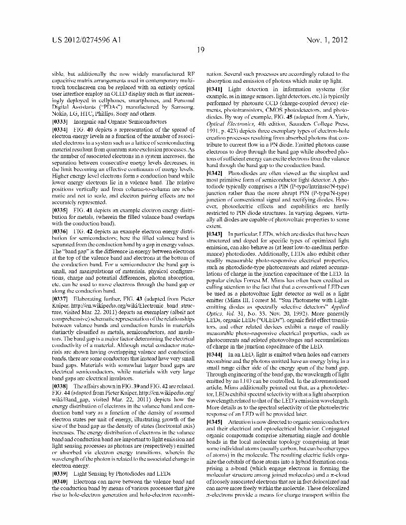
US 2012/0274596 Al
sible, but additionally the now widely manufactured RFcapacitive matrix arrangements used in contemporary multi-touch touchscreen can be replaced with an entirely opticaluser interface employ an OLED display such as that increas-ingly deployed in cellphones, smartphones, and PersonalDigital Assistants ("PDAs") manufactured by Samsung,Nokia, LG, HTC, Phillips, Sony and others.[0333] Inorganic and Organic Semiconductors[0334] FIG. 40 depicts a representation of the spread ofelectron energy levels as a function of the number of associ-ated electrons in a system such as a lattice of semiconductingmaterial resultant from quantum state exclusion processes. Asthe number of associated electrons in a system increases, theseparation between consecutive energy levels decreases, inthe limit becoming an effective continuum of energy levels.Higher energy level electrons form a conduction band whilelower energy electrons lie in a valence band. The relativepositions vertically and from colunm-to-colunm are sche-matic and not to scale, and electron pairing effects are notaccurately represented.[0335] FIG. 41 depicts an example electron energy distri-bution for metals, (wherein the filled valance band overlapswith the conduction band).[0336] FIG. 42 depicts an example electron energy distri-bution for semiconductors; here the filled valance band isseparated from the conduction band by a gap in energy values.The "band gap" is the difference in energy between electronsat the top of the valence band and electrons at the bottom ofthe conduction band. For a semiconductor the band gap issmall, and manipulations of materials, physical configura-tions, charge and potential differences, photon absorption,etc. can be used to move electrons through the band gap oralong the conduction band.[0337] Elaborating further, FIG. 43 (adapted from PieterKuiper, http://en.wikipedia.org/wiki/Electronic_band_struc-ture, visited Mar. 22, 2011) depicts an exemplary (albeit notcomprehensive) schematic representation of the relationshipsbetween valance bands and conduction bands in materialsdistinctly classified as metals, semiconductors, and insula-tors. The band gap is a major factor determining the electricalconductivity of a material. Although metal conductor mate-rials are shown having overlapping valance and conductionbands there are some conductors that instead have very smallband gaps. Materials with somewhat larger band gaps areelectrical semiconductors, while materials with very largeband gaps are electrical insulators.[0338] The affairs shown in FIG. 39 and FIG. 42 are related.FIG. 44 (adapted from Pieter Kuiper, http://en.wikipedia.org/wiki/Band_gap, visited Mar. 22, 2011) depicts how theenergy distribution of electrons in the valance band and con-duction band vary as a function of the density of assumedelectron states per unit of energy, illustrating growth of thesize of the band gap as the density of states (horizontal axis)increases. The energy distribution of electrons in the valanceband and conduction band are important to light emission andlight sensing processes as photons are (respectively) emittedor absorbed via electron energy transitions, wherein thewavelength of the photon is related to the associated change inelectron energy.[0339] Light Sensing by Photodiodes and LEDs[0340] Electrons can move between the valence band andthe conduction band by means of various processes that giverise to hole-electron generation and hole-electron recombi-
Nov. 1,201219
nation. Several such processes are accordingly related to theabsorption and emission of photons which make up light.[0341] Light detection in information systems (forexample, as in image sensors, light detectors, etc.) is typicallyperformed by photo site CCD (charge-coupled device) ele-ments, phototransistors, CMOS photodetectors, and photo-diodes. By way of example, FIG. 45 (adapted from A. Yariv,Optical Electronics, 4th edition, Saunders College Press,1991, p. 423) depicts three exemplary types of electron-holecreation processes resulting from absorbed photons that con-tribute to current flow in a PN diode. Emitted photons causeelectrons to drop through the band gap while absorbed pho-tons of sufficient energy can excite electrons from the valanceband though the band gap to the conduction band.[0342] Photodiodes are often viewed as the simplest andmost primitive form of semiconductor light detector. A pho-todiode typically comprises a PIN (P-type/Intrinsic/N-type)junction rather than the more abrupt PIN (P-type/N-type)junction of conventional signal and rectifying diodes. How-ever, photoelectric effects and capabilities are hardlyrestricted to PIN diode structures. In varying degrees, virtu-ally all diodes are capable of photovoltaic properties to someextent.[0343] In particular, LEDs, which are diodes that have beenstructured and doped for specific types of optimized lightemission, can also behave as (at least low-to-medium perfor-mance) photodiodes. Additionally, LEDs also exhibit otherreadily measurable photo-responsive electrical properties,such as photodiode-type photo currents and related accumu-lations of charge in the junction capacitance of the LED. Inpopular circles Forrest M. Mims has often been credited ascalling attention to the fact that that a conventional LED canbe used as a photovoltaic light detector as well as a lightemitter (Mims III, Forrest M. "Sun Photometer with Light-emitting diodes as spectrally selective detectors" AppliedOptics, Vol. 31, No. 33, Nov. 20, 1992). More generallyLEDs, organic LEDs ("OLEDs"), organic field effect transis-tors, and other related devices exhibit a range of readilymeasurable photo-responsive electrical properties, such asphoto currents and related photovoltages and accumulationsof charge in the junction capacitance of the LED.[0344] In an LED, light is emitted when holes and carriersrecombine and the photons emitted have an energy lying in asmall range either side of the energy span of the band gap.Through engineering of the band gap, the wavelength oflightemitted by an LED can be controlled. In the aforementionedarticle, Mims additionally pointed out that, as a photodetec-tor, LEDs exhibit spectral selectivity with at a light absorptionwavelength related to that of the LED's emission wavelength.More details as to the spectral selectivity of the photoelectricresponse of an LED will be provided later.[0345] Attention is now directed to organic semiconductorsand their electrical and optoelectrical behavior. Conjugatedorganic compounds comprise alternating single and doublebonds in the local molecular topology comprising at leastsome individual atoms (usually carbon, but can be other typesof atoms) in the molecule. The resulting electric fields orga-nize the orbitals of those atoms into a hybrid formation com-prising a a-bond (which engage electrons in forming themolecular structure among joined molecules) and a rt-cloudofloosely associated electrons that are in fact delocalized andcan move more freely within the molecule. These delocalizedn-electrons provide a means for charge transport within the

US 2012/0274596 Al
molecule and electric current within larger-structures oforganic materials (for example, polymers).[0346] Combinations of atomic orbital modalities for theindividual atoms in a molecule, together with the moleculartopology (defined by the network of a-bonds) and moleculargeometry, create molecule-scale orbitals for the delocalizedrt-cloud of electrons and in a sense for the electrons compris-ing a-bonds. Interactions among the electrons, in particularquantum exclusion processes, create an energy gap betweenthe Highest Occupied Molecular Orbital ("HOMO") andLowest-Unoccupied Molecular Orbital ("LUMO") for thedelocalized Jt electrons (and similarly does so for the morehighly localized a-bond electrons). FIG. 46 (adapted from Y.Divayana, X. Sung, Electroluminescence in Organic Light-Emitting Diodes, VDM Verlag Dr. Muller, Saarbrucken,2009, ISBN 978-3-639-17790-9, FIG. 2.2, p. 13) depicts theelectron energy distribution among bonding (Jt and a) andantibonding (Jt* and a*) molecular orbitals in for two elec-trons in an exemplary conjugated or aromatic organic com-pound. In such materials, typically the energy gap betweenthe Jt and Jt* molecular orbitals correspond to the gap betweenthe HOMO and LUMO. The HOMO effectively acts as avalence band in a traditional (inorganic) crystal lattice semi-conductor and the LUMO acts as effective equivalent to aconduction band. Accordingly, energy gap between theHOMO and LUMO (usually corresponding to the gapbetween the Jt and Jt* molecular orbitals) behaves in a mannersimilar to the band gap in a crystal lattice semiconductor andthus permits many aromatic organic compounds to serve aselectrical semiconductors.[0347] Emitted photons cause electrons to drop through theHOMO/LUMO gap while absorbed photons of sufficientenergy can excite electrons from the HOMO to the LUMO.These processes are similar to photon emission and photoabsorption processes in a crystal lattice semiconductor andcan be used to implement organic LED ("OLED") andorganic photodiode effects with aromatic organic com-pounds. Functional groups and other factors can vary thewidth of the band gap so that it matches energy transitionsassociated with selected colors of visual light. Additionaldetails on organic LED ("OLED") processes, materials,operation, fabrication, performance, and applications can befound in, for example:
[0348] Z. Li, H. Ming (eds.), Organic Light-EmittingMaterials and Devices, CRC Taylor & Francis, BocaRaton, 2007, ISBN 1-57444-574-X;
[0349] Z. Kafafi (ed.), Organic Electroluminescence,CRC Taylor & Francis, Boca Raton, 2005, ISBN0-8247 -5906-0;
[0350] Y. Divayana, X. Sung, Electroluminescence inOrganic Light-Emitting Diodes, VDM Verlag Dr.Muller, Saarbrucken, 2009, ISBN 978-3-639-17790-9.
[0351] It is noted that an emerging alternative to OLEDs areOrganic Light Emitting Transistors (OLETS). The presentinvention allows for arrangements employing OLETS to beemployed in place ofOLEDs and inorganic LEDs as appro-priate and advantageous wherever mentioned throughout thespecification.[0352] Potential Co-Optimization of Light Sensing andLight Emitting Capabilities of an Optical Diode Element[0353] FIG. 47 depicts an optimization space 4700 forsemiconductor (traditional crystal lattice or organic material)diodes comprising attributes of signal switching perfor-mance, light emitting performance, and light detection per-
Nov. 1,201220
formance. Specific diode materials, diode structure, anddiode fabrication approaches 4723 can be adjusted to opti-mize a resultant diode for switching function performance4701 (for example, via use of abrupt junctions), light detec-tion performance 4702 (for example via a P-I-N structurecomprising a layer of intrinsic semiconducting materialbetween regions of n-type and p-type material, or light detec-tion performance 4703.[0354] FIG. 48 depicts an exemplary "metric space" 4800of device realizations for optoelectronic devices and regionsof optimization and co-optimization.[0355] Specific optoelectrical diode materials, structure,and fabrication approaches 4823 can be adjusted to optimizea resultant optoelectrical diode for light detection perfor-mance 4801 (for example via a P-I-N structure comprising alayer of intrinsic semiconducting material between regions ofn-type and p-type material versus light emission performance4802 versus cost 4803. Optimization within the plane definedby light detection performance 4801 and cost 4803 tradition-ally result in photodiodes 4811 while optimization within theplane defined by light emission performance 4802 and cost4803 traditionally result in LEDs 4812. The present inventionprovides for specific optoelectrical diode materials, structure,and fabrication approaches 4823 to be adjusted to co-opti-mize an optoelectrical diode for both good light detectionperformance 4801 and light emission performance 4802 ver-sus cost 4803. A resulting co-optimized optoelectrical diodecan be used for multiplexed light emission and light detectionmodes. These permit a number of applications as explained inthe sections to follow.[0356] Again it is noted that an emerging alternative toOLEDs are Organic Light Emitting Transistors (OLETS).The present invention allows for arrangements employingOLETS to be employed in place of OLEDs and inorganicLEDs as appropriate and advantageous wherever mentionedthroughout the specification.[0357] Electronic Circuit Interfacing to LEDs Used asLight Sensors[0358] FIGS. 49-52 depict various exemplary circuits dem-onstrating various exemplary approaches to detecting lightwith an LED. These initially introduce the concepts ofreceived light intensity measurement ("detection") and vary-ing light emission intensity of an LED in terms of variationsin D.C. ("direct-current") voltages and currents. However,light intensity measurement ("detection") can be accom-plished by other means such as LED capacitance effects-forexample reverse-biasing the LED to deposit a known charge,removing the reverse bias, and then measuring the time for thecharge to then dissipate within the LED. Also, varying thelight emission intensity of an LED can be accomplished byother means such as pulse-width-modulation-for example,a duty-cycle of 50% yields 50% of the "constant-on" bright-ness, a duty-cycle of 50% yields 50% of the "constant-on"brightness, etc. These, too, are provided for by the inventionand will be considered again later as variations of the illus-trative approaches provided below.[0359] To begin, LED1 in FIG. 49 is employed as a photo-diode, generating a voltage with respect to ground responsiveto the intensity of the light received at the optically-exposedportion of the LED-structured semiconducting material. Inparticular, for at least a range of light intensity levels thevoltage generated by LED 1 increases monotonically with thereceived light intensity. This voltage can be amplified by ahigh-impedance amplifier, preferably with low offset cur-

US 2012/0274596 Al
rents. The example of FIG. 49 shows this amplification per-formed by a simple operational amplifier ("op amp") circuitwith fractional negative feedback, the fraction determined viaa voltage divider. The gain provided by this simple op amparrangement can be readily recognized by one skilled in theart as
l+(RJRg).
[0360] The op amp produces an isolated and amplified out-put voltage that increases, at least for a range, monotonicallywith increasing light received at the light detection LED1.Further in this example illustrative circuit, the output voltageof the op amp is directed to LED100 via current-limitingresistor R100. The result is that the brightness oflight emittedby LED100 varies with the level oflight received by LED1.[0361] For a simple lab demonstration of this ratherremarkable fact, one can choose a TL08x series (TL082,TL084, etc.) or equivalent op amp powered by +12 and -12volt split power supply, R100 of -1 KQ, and RJRg in a ratioranging from 1 to 20 depending on the type of LED chosen.LED100 will be dark when LED1 is engulfed in darkness andwill be brightly lit when LED1 is exposed to natural levels ofambient room light. For best measurement studies, LED1could comprise a "water-clear" plastic housing (rather thancolor-tinted). It should also be noted that the LED1 connec-tion to the amplifier input is of relatively quite high imped-ance and as such can readily pick up AC fields, radio signals,etc. and is best realized using as physically small electricalsurface area and length as possible. In a robust system, elec-tromagnetic shielding is advantageous.[0362] The demonstration circuit of FIG. 49 can beimproved, modified, and adapted in various ways (forexample, by adding voltage and/or current offsets, JFETpreamplifiers, etc.), but as shown is sufficient to show that awide range of conventional LEDs can serve as pixel sensorsfor an ambient-room light sensor array as can be used in acamera or other room-light imaging system. Additionally,LED100 shows the role an LED can playas a pixel emitter oflight.[0363] FIG. 50 shows a demonstration circuit for the pho-tocurrent of the LED. For at least a range of light intensitylevels the photo current generated by LED1 increases mono-tonically with the received light intensity. In this exemplarycircuit the photocurrent is directed to a natively high-imped-ance op amp (for example, a FET input op amp such as therelatively well-known LF -351) set up as an inverting current-to-voltage converter. The magnitude of the transresistance(i.e., the current-to-voltage "gain") of this inverting current-to-voltage converter is set by the value of the feedback resistorRf. The resultant circuit operates in a similar fashion to that ofFIG. 49 in that the output voltage of the op amp increases, atleast for a range, monotonically with increasing light receivedat the light detection LED. The inverting current-to-voltageconverter inverts the sign of the voltage, and such inversion insign can be corrected by a later amplification stage, useddirectly, or is preferred. In other situations it can be advanta-geous to not have the sign inversion, in which case the LEDorientation in the circuit can be reversed, as shown in FIG. 51.[0364] FIG. 52 shows an illustrative demonstrationarrangement in which an LED can be for a very short durationof time reverse biased and then in a subsequent interval oftime the resultant accumulations of charge in the junctioncapacitance of the LED are discharged. The decrease incharge during discharge through the resistor R results in a
Nov. 1,201221
voltage that can be measured with respect to a predeterminedvoltage threshold, for example as can be provided by a (non-hysteretic) comparator or (hysteretic) Schmitt-trigger. Theresulting variation in discharge time varies monotonicallywith the light received by the LED. The illustrative demon-stration arrangement provided in FIG. 52 is further shown inthe context of connects to the bidirectional I/O pin circuit fora conventional microprocessor. This permits the principal tobe readily demonstrated through a simple software programoperating on such a microprocessor. Additionally, as will beseen later, the very same circuit arrangement can be used tovariably control the emitted light brightness of the LED bymodulating the temporal pulse-width of a binary signal at oneor both of the microprocessor pins.[0365] Multiplexing Circuitry for LED Arrays[0366] For rectangular arrays ofLEDs, it is typically usefulto interconnect each LED with access wiring arranged to bepart of a corresponding matrix wiring arrangement. Thematrix wiring arrangement is time-division multiplexed.Such time-division multiplexed arrangements can be used fordelivering voltages and currents to selectively illuminate eachindividual LED at a specific intensity level (including verylow or zero values so as to not illuminate).[0367] An example multiplexing arrangement for a two-dimensional array ofLEDs is depicted in FIG. 53. Here eachof a plurality of normally-open analog switches are sequen-tially closed for brief disjointed intervals of time. This allowsthe selection of a particular subset (here, a colunm) ofLEDsto be grounded while leaving all other LEDs in the array notconnected to ground. Each of the horizontal lines then can beused to connect to exactly one grounded LED at a time. Theplurality of normally-open analog switches in FIG. 53 can becontrolled by an address decoder so that the selected subsetcan be associated with a unique binary address, as suggestedin FIG. 54. The combination of the plurality of normally -openanalog switches together with the address decoder form ananalog line selector. By connecting the line decoder's addressdecoder input to a counter, the columns of the LED array canbe sequentially scanned.[0368] FIG. 55 depicts an exemplary adaptation of thearrangement of FIG. 54 together to form a highly scalableLED array display that also functions as a light field detector.The various multiplexing switches in this arrangement can besynchronized with the line selector and mode control signalso that each LED very briefly provides periodically updateddetection measurement and is free to emit light the rest of thetime. A wide range of variations and other possible imple-mentations are possible and implemented in various products.[0369] Such time-division multiplexed arrangements canalternatively be used for selectively measuring voltages orcurrents of each individual LED. Further, the illuminationand measurement time-division multiplexed arrangementsthemselves can be time-division multiplexed, interleaved, ormerged in various ways. As an illustrative example, thearrangement of FIG. 55 can be reorganized so that the LED,mode control switch, capacitor, and amplifiers are collocated,for example as in the illustrative exemplary arrangement ofFIG. 56. Such an arrangement can be implemented with, forexample, three MOSFET switching transistor configurations,two MOSFET amplifying transistor configurations, a small-area/small-volume capacitor, and an LED element (that is,five transistors, a small capacitor, and an LED). This can betreated as a cell which is interconnected to multiplexingswitches and control logic. A wide range of variations and

US 2012/0274596 Al
other possible implementations are possible and the exampleof FIG. 55 is in no way limiting. For example, the arrange-ment of FIG. 55 can be reorganized to decentralize the mul-tiplexing structures so that the LED, mode control switch,multiplexing and samplelhold switches, capacitor, and ampli-fiers are collocated, for example as in the illustrative exem-plary arrangement of FIG. 57. Such an arrangement can beimplemented with, for example, three MOSFET switchingtransistor configurations, two MOSFET amplifying transistorconfigurations, a small-area/small-volume capacitor, and anLED element (that is, five transistors, a small capacitor, andan LED). This can be treated as a cell whose analog signalsare directly interconnected to busses. Other arrangements arealso possible.[0370] The discussion and development thus far are basedon the analog circuit measurement and display arrangementof FIG. 49 that in tum leverages the photovoltaic properties ofLEDs. With minor modifications clear to one skilled in the art,the discussion and development thus far can be modified tooperate based on the analog circuit measurement and displayarrangements of FIG. 50 and FIG. 51 that leverage the pho-tocurrrent properties ofLEDs.[0371] FIGS. 58-60 depict an example of how the digitalcircuit measurement and display arrangement of FIG. 52 (thatin turn leverages discharge times for accumulations of photo-induced charge in the junction capacitance of the LED) can beadapted into the construction developed thus far. FIG. 58adapts FIG. 52 to additional include provisions for illuminat-ing the LED with a pulse-modulated emission signal. Notingthat the detection process described earlier in conjunctionwith FIG. 52 can be confined to unperceivably short intervalsof time, FIG. 59 illustrates how a pulse-width modulatedbinary signal can be generated during LED illumination inter-vals to vary LED emitted light brightness. FIG. 60 illustratesan adaptation of the tri-state and Schmitt-trigger/comparatorlogic akin to that illustrated in the microprocessor I/O pininterface that can be used to sequentially access subsets ofLEDs in an LED array as described in conjunction with FIG.53 and FIG. 54.[0372] FIG. 61-63 depict exemplary state diagrams for theoperation of the LED and the use of input signals and outputsignals described above. From the viewpoint of the binarymode control signal there are only two states: a detection stateand an emission state, as suggested in FIG. 61. From theviewpoint of the role of the LED in a larger system incorpo-rating a multiplexed circuit arrangement such as that of FIG.55, there can a detection state, an emission state, and an idlestate (where there is no emission nor detection occurring),obeying state transition maps such as depicted in FIG. 62 orFIG. 63. At a further level of detail, there are additionalconsiderations:
[0373] To emit light, a binary mode control signal can beset to "emit" mode (causing the analog switch to beclosed) and the emission light signal must be of suffi-cient value to cause the LED to emit light (for example,so that the voltage across the LED is above the "tum-on"voltage for that LED).[0374] If the binary mode control signal is in "emit"
mode but the emission light signal is not of suchsufficient value, the LED will not illuminate. This canbe useful for brightness control (via pulse-widthmodulation), black-screen display, and other uses. Insome embodiments, this can be used to coordinate the
Nov. 1,201222
light emission of neighboring LEDs in an array whilea particular LED in the array is in detection mode.
[0375] If the emission light signal of such sufficientvalue but the binary mode control signal is in "detect"mode, the LED will not illuminate responsive to theemission light signal. This allows the emission lightsignal to be varied during a time interval when there isno light emitted, a property useful for multiplexingarrangements.
[0376] During a time interval beginning with the changeof state of the binary mode control signal to some set-tling-time period afterwards, the detection output and/orlight emission level can momentarily not be accurate.
[0377] To detect light, the binary mode control signalmust be in "detect" mode (causing the analog switch tobe open). The detected light signal can be used by asubsequent system or ignored. Intervals where the cir-cuit is in detection mode but the detection signal isignored can be useful for multiplexing arrangement, inproviding guard-intervals for settling time, to coordinatewith the light emission of neighboring LEDs in an array,etc.
[0378] FIG. 64 depicts an exemplary state transition dia-gram reflecting the above considerations. The top "EmitMode" box and bottom "Detect Mode" box reflect the statesof an LED from the viewpoint of the binary mode controlsignal as suggested by FIG. 61. The two "Idle" states (one ineach of the "Emit Mode" box and "Detect Mode" box) ofFI G.64 reflect (at least in part) the "Idle" state suggested in FIG. 62and/or FIG. 63. Within the "Emit Mode" box, transitionsbetween "Emit" and "Idle" can be controlled by emit signalmultiplexing arrangements, algorithms for coordinating thelight emission of an LED in an array while a neighboring LEDin the array is in detection mode, etc. Within the "DetectMode" modality, transitions between "Detect" and "Idle" canbe controlled by independent or coordinated multiplexingarrangements, algorithms for coordinating the light emissionof an LED in an array while a neighboring LED in the array isin detection mode, etc. In making transitions between statesin the boxes, the originating and termination states can bechosen in a manner advantageous for details of various mul-tiplexing and feature embodiments. Transitions between thegroups of states within the two boxes correspond to the vastimpedance shift invoked by the switch opening and closing asdriven by the binary mode control signal. In FIG. 64, thesettling times between these two groups of states are gatheredand regarded as a transitional state.[0379] As mentioned earlier, the amplitude oflight emittedby an LED can be modulated to lesser values by means ofpulse-width modulation (PWM) of a binary waveform. Forexample, if the binary waveform oscillates between fullyilluminated and non-illuminated values, the LED illumina-tion amplitude will be perceived roughly as 50% of the full-onillumination level when the duty-cycle of the pulse is 50%,roughly as 75% of the full-on illumination level when theduty-cycle of the pulse is 75%, roughly as 10% of the full-onillumination level when the duty-cycle of the pulse is 10%,etc. Clearly the larger fraction of time the LED is illuminated(i.e., the larger the duty-cycle), the brighter the perceived lightobserved emitted from the LED.[0380] Use ofa LED Array as "Multi-Touch" Tactile Sen-sor Array[0381] Multi-touch sensors on cellphones, smartphones,PDAs, tablet computers, and other such devices typically

US 2012/0274596 Al
utilize a capacitive matrix proximity sensor. Typically a trans-parent capacitive matrix proximity sensor is overlaid over anLCD display, which is in tum overlaid on a (typically LED)backlight used to create and direct light though the LCDdisplay from behind. Each of the capacitive matrix and theLCD have considerable associated electronic circuitry andsoftware associated with them.[0382] FIG. 66 depicts an exemplary modification of thearrangement depicted in FIG. 65 wherein the LCD displayand backlight are replaced with an OLED array used as avisual display. Such an arrangement has started to be incor-porated in recent contemporary cell phone, smartphone, PDA,tablet computers, and other portable device products by sev-eral manufacturers. Note the considerable reduction in opto-electronic, electronic, and processor components. This is oneof the motivations for using OLED displays in these emergingproduct implementations.[0383] FIG. 67 depicts an exemplary arrangement providedfor by the invention comprising only a LED array. In generalthe LEDs in the LED array can be OLEDs or inorganic LEDs.In an embodiment provided for by the invention, such anarrangement can be used as a tactile user interface, or as acombined a visual display and tactile user interface, as will bedescribed. Note the considerable reduction in optoelectronic,electronic, and processor components over the both thearrangement depicted in FIG. 65 and the arrangementdepicted in FIG. 66. This is one of among the many advan-tages of the various embodiments and adaptations of thepresent invention, as will be described.[0384] Arrays of inorganic-LEDs have been used to createa tactile proximity sensor array as taught by Han in U.S. Pat.No. 7,598,949 and depicted in the video available at http://cs.nyu.edu/.aboutjhanlledtouchlindex.html). Pending U.S.patent application Ser. No. 12/418,605 teaches several adap-tations and enhancements of such an approach, includingconfiguring the operation of an LED array to emit modulatedlight that is modulated at a particular carrier frequency and/orwith a particular time-variational waveform and respond toonly modulated light signal components extracted from thereceived light signals comprising that same carrier frequencyor time-variational waveform (so as to reject potential inter-ference from ambient light in the surrounding user environ-ment). As described earlier, FIG. 9 depicts a representativeexemplary arrangement wherein light emitted by neighboringLEDs is reflected from a finger (or other object) back to anLED acting as a light sensor.[0385] In its most primitive form, such LED-array tactileproximity array implementations need to be operated in adarkened environment (as seen in the video available at http://cs.nyu.edu/.aboutjhanlledtouchlindex.html). The inventionprovides for additional systems and methods for not requiringdarkness in the user environment in order to operate the LEDarray as a tactile proximity sensor.[0386] As taught in pending U.S. patent application Ser.No. 12/418,605, potential interference from ambient light inthe surrounding user environment can be limited by using anopaque pliable and/or elastically deformable surface cover-ing the LED array that is appropriately reflective (direction-ally, amorphously, etc. as can be advantageous in a particulardesign) on the side facing the LED array. Such a system andmethod can be readily implemented in a wide variety of waysas is clear to one skilled in the art.[0387] Also as taught in pending U.S. patent applicationSer. No. 12/418,605, potential interference from ambient
Nov. 1,201223
light in the surrounding user environment can be limited byemploying amplitude, phase, or pulse width modulated cir-cuitry and/or software to control the light emission andreceiving process. For example, in an implementation theLED array can be configured to emit modulated light that ismodulated at a particular carrier frequency and/or with aparticular time-variational waveform and respond to onlymodulated light signal components extracted from thereceived light signals comprising that same carrier frequencyor time-variational waveform. Such a system and method canbe readily implemented in a wide variety of ways as is clear toone skilled in the art.[0388] In various embodiments and alternative implemen-tations provided for by the invention, light measurementsused for implementing a tactile user interface can be fromunvignetted LEDs, unvignetted photodiodes, vignettedLEDs, vignetted photodiodes, or combinations of two ormore of these.[0389] Pending U.S. patent application Ser. No. 12/418,605 further teaches application of such LED-based tactilesensor for use as a touch sensor in an HDTP implementationthat provides single-touch and multi-touch measurement offinger contact angles and downward pressure. The perfor-mance of such features can advantageously improve withincreases in spatial resolution of the tactile sensor. U.S. patentapplication Ser. No. 12/418,605 additionally teaches furtherconsiderations and accommodations for interacting with highspatial resolution tactile image measurements, particularly insituations involving multi-touch and/or parts of the hand andfingers other than fingertips. Further, pending U.S. patentapplication Ser. No. 13/180,345 teaches among other thingsvarious physical, electrical, and operational approaches tointegrating a touchscreen with OLED arrays, displays, inor-ganic LED arrays, and LCDs, etc. as well as using sucharrangements to integrate other applications. It is also notedthat pending U.S. patent application Ser. No. 111761,978(priority date May 15, 1999) teaches a gesture-based touch-screen employing a transparent tactile sensor.[0390] One aspect of the present invention is directed tousing an OLED array as a high spatial resolution of the tactilesensor.[0391] Another aspect of the present invention is directed tousing an OLED array as both a display and as a high spatialresolution of the tactile sensor.[0392] Another aspect of the present invention is directed tousing an OLED array as a high spatial resolution tactile sensorin touchscreen implementation.[0393] Another aspect of the present invention is directed tousing an OLED array as both a display and as a high spatialresolution tactile sensor in touchscreen implementation.[0394] Another aspect of the present invention is directed tousing an OLED array as a high spatial resolution tactile sensorin a touch-based user interface that provides multi-touchcapabilities.[0395] Another aspect of the present invention is directed tousing an OLED array as both a display and as a high spatialresolution tactile sensor in a touch-based user interface thatprovides multi-touch capabilities.[0396] Another aspect of the present invention is directed tousing an OLED array as a high spatial resolution tactile sensorin an HDTP implementation.[0397] Another aspect of the present invention is directed tousing an OLED array as both a display and as a high spatialresolution tactile sensor in an HDTP implementation.

US 2012/0274596 Al
[0398] Another aspect of the present invention is directed tousing an OLED array as a high spatial resolution tactile sensorin a touch-based user interface that provides at least single-touch measurement of finger contact angles and downwardpressure.[0399] Another aspect of the present invention is directed tousing an OLED array as both a display and as a high spatialresolution tactile sensor in a touch-based user interface thatprovides at least single-touch measurement of finger contactangles and downward pressure.[0400] Another aspect of the present invention is directed tousing an OLED array as a high spatial resolution tactile sensorin a touch-based user interface that provides at least single-touch measurement of finger contact angles with the touchsensor.[0401] Another aspect of the present invention is directed tousing an OLED array as both a display and as a high spatialresolution tactile sensor in a touch-based user interface thatprovides at least single-touch measurement of finger contactangles with the touch sensor.[0402] Another aspect of the present invention is directed tousing an OLED array as a high spatial resolution tactile sensorin a touch-based user interface that provides at least single-touch measurement of downward pressure asserted on thetouch sensor by a user finger.[0403] Another aspect of the present invention is directed tousing an OLED array as both a display and as a high spatialresolution tactile sensor in a touch-based user interface thatprovides at least single-touch measurement of downwardpressure asserted on the touch sensor by a user finger.[0404] Another aspect of the present invention provides atouch interface system for the operation by at least one finger,the touch interface physically associated with a visual dis-play, the system comprising a processor executing at least onesoftware algorithm, and a light emitting diode (LED) arraycomprising a plurality of transparent organic light emittingdiodes (OLEDs) forming a transparent OLED array, thetransparent OLED array configured to communicate with theprocessor. The at least one software algorithm is configured tooperate at least a first group ofOLEDS from the transparentOLED array in at least a light sensing mode. The OLEDs inthe at least a first group of OLEDs are configured to detectlight using a photoelectric effect when light is received for aninterval of time and communicates the light detection to theprocessor. The at least one software algorithm is configured toproduce tactile measurement information, the tactile mea-surement information responsive to light reflected by at leasta finger proximate to the OLED array, and a portion of thereflected light is reflected to at least one OLED of the firstgroup of the transparent OLED array, the reflected light origi-nating from a software-controlled light source. The processoris configured to generate at least one control signal responsiveto light reflected by at least one finger proximate to the 0 LEDarray.[0405] In another aspect of the present invention, the soft-ware-controlled light source is another LED array.[0406] In another aspect of the present invention, the LEDarray is acting as the software-controlled light source isanother OLED array.[0407] In another aspect of the present invention, the soft-ware-controlled light source is implemented by a secondgroup of the transparent OLEDs from the transparent OLEDarray.
Nov. 1,201224
[0408] In another aspect of the present invention, the firstgroup ofOLEDs and the second group ofOLEDs are distinct.[0409] In another aspect of the present invention, the firstgroup of the transparent OLEDs and the second group of thetransparent OLEDs both comprise at least one OLED thatcommon to both groups.[0410] In another aspect of the present invention, the firstgroup of the transparent OLEDs and the second group of thetransparent OLEDs are the same group.[0411] In another aspect of the present invention, the trans-parent OLED array is configured to perform light sensing forat least an interval of time.[0412] In another aspect of the present invention, the soft-ware-controlled light source comprises a Liquid Crystal Dis-play.[0413] In another aspect of the present invention, the pro-cessor and the at least one software algorithm are configuredto operate the transparent OLED array in a light emittingmode.[0414] In another aspect of the present invention, the soft-ware-controlled light source is configured to emit modulatedlight.[0415] In another aspect of the present invention, thereflected light comprises the modulated light.[0416] In another aspect of the present invention, the sys-tem is further configured to provide the at least one controlsignal responsive to the reflected light.[0417] In another aspect of the present invention, the sys-tem is further configured so that the at least one control signalcomprises a high spatial resolution reflected light measure-ment responsive to the reflected light.[0418] In another aspect of the present invention, the sys-tem is used to implement a tactile user interface.[0419] In another aspect of the present invention, the sys-tem is used to implement a touch-based user interface.[0420] In another aspect of the present invention, the sys-tem is used to implement a touchscreen.[0421] In another aspect of the invention, the processor isconfigured to generate at least one control signal responsiveto changes in the light reflected by at least one finger proxi-mate to the OLED array.[0422] In another aspect of the invention, the processor isconfigured to generate at least one control signal responsiveto a touch gesture performed by at least one finger proximateto the OLED array.[0423] Example Physical Configurations for Tactile Sensorand Display Arrangements[0424] The capabilities described thus far can be combinedwith systems and techniques to be described later in a varietyof physical configurations and implementations. A number ofexample physical configurations and implementations aredescribed here and in pending U.S. patent application Ser.No. 13/180,345 that provide various advantages to variousembodiments, implementations, and applications of thepresent invention. Many variations and alternatives are pos-sible and are accordingly anticipated by the invention, and theexample physical configurations and implementations are inno way limiting of the invention.[0425] Attention is first directed to arrangements wherein asingle LED array-such as an OLED display, other OLEDarray, inorganic LED array, inorganic LED display, etc.-isconfigured to operate as both a display and a touch sensor (forexample for use as a touchscreen) and various generalizationsof these. The earlier discussion associated with FIG. 67, for

US 2012/0274596 Al
example, relates to an OLED array implementation relevantto such arrangements. There are at least two approaches forimplementing such arrangements (wherein a single LEDarray-such as an OLED display, other OLED array, inor-ganic LED array, inorganic LED display, etc.-is configuredto operate as both a display and a touch sensor (for example atouchscreen).
[0426] In a first example approach, the inorganic LEDsor OLEDs comprised by an (inorganic LED or OLED)LED array are partitioned into two subsets. One subset isemployed as a display, while the other subset isemployed as a tactile sensor. In various embodiments,individual elements of the two subsets can be spatiallyinterleaved in various ways-for example in co-planar,non-coplanar, stacked, or other arrangements. FIG. 68adepicts an example arrangement wherein an (inorganicLED or OLED) LED array is partitioned into two sub-sets, one subset employed as a visual display and theother subset employed as a tactile sensor.
[0427] In a second example approach, the inorganicLEDs or OLEDs comprised by an (inorganic LED orOLED) LED array are multiplexed between or among atleast a light emitting mode and a light sensing mode. Thelight emitting mode is used for both visual display andtactile-sensor touch-area illumination, and the lightsensing mode is used for tactile sensing. FIG. 68bdepicts an arrangement wherein inorganic LEDs orOLEDs comprised by an (inorganic LED or OLED)LED array are multiplexed between or among at least alight emitting mode and a light sensing mode.
Various other implementations are possible, for example vari-ous combinations[0428] Attention is now directed to arrangements wherein atransparent LED array (inorganic LED or OLED), forexample implemented with arrays of transparent OLEDsinterconnected with transparent conductors, is overlaid atopan LCD display, and various generalizations of this. Thetransparent conductors can for example be comprised ofmaterials such as indium tin oxide, fluorine-doped tin oxide("FTO"), doped zinc oxide, organic polymers, carbon nano-tubes, graphene ribbons, etc. There are at least threeapproaches for implementing such arrangements wherein atransparent LED array (inorganic LED or OLED), forexample implemented with arrays of transparent OLEDsinterconnected with transparent conductors, is overlaid atopan LCD display.
[0429] In a first example approach, the inorganic LEDsor OLEDs comprised by an (inorganic LED or OLED)LED array are used only in light sensing mode for tactilesensing, and the LCD is used for both a visual displayand tactile-sensor touch-area illumination.
[0430] In a second example approach, the inorganicLEDs or OLEDs comprised by an (inorganic LED orOLED) LED array are partitioned into two subsets. Onesubset is employed as a display, while the other subset isemployed as a tactile sensor. In various embodimentsindividual elements of the two subsets can be spatiallyinterleaved in various ways-for example in co-planar,non-coplanar, stacked, or other arrangements. The LCDis used only as a visual display.
[0431] In a third example approach, the inorganic LEDsor OLEDs comprised by an (inorganic LED or OLED)LED array are multiplexed between or among at least alight emitting mode and a light sensing mode. The light
Nov. 1,201225
emitting mode is used for tactile-sensor touch-area illu-mination, and the light sensing mode is used for tactilesensing. The LCD is used only as a visual display.
FIG. 69a depicts an example arrangement wherein a trans-parent (inorganic LED or OLED) LED array is used as atouch sensor, and overlaid atop an LCD display. Various otherimplementations are possible, for example various combina-tions[0432] FIG. 69b depicts an example implementation com-prising a transparent OLED array overlaid upon an LCDvisual display, which is in tum overlaid on a (typically) LEDbacklight used to create and direct light though the LCDvisual display from behind. Such an arrangement can be usedto implement an optical tactile user interface arrangement asenabled by the present invention. Other related arrangementsand variations are possible and are anticipated by the inven-tion. The invention provides for inclusion of coordinatedmultiplexing or other coordinated between the OLED arrayand LCD as needed or advantageous. It is noted in oneembodiment the LCD and LED array can be fabricated on thesame substrate, the first array layered atop the second (or visaversa) while in another embodiment the two LED arrays canbe fabricated separately and later assembled together to formlayered structure. Other related arrangements and variationsare possible and are anticipated by the invention.[0433] Attention is now directed to arrangements wherein afirst transparent (inorganic LED or OLED) LED array isoverlaid upon a second (inorganic LED or OLED) LED array,and various variations and generalizations of this. There are atleast three approaches for implementing such arrangementsand several variations wherein a first transparent (inorganicLED or OLED) LED array is overlaid upon a second (inor-ganic LED or OLED) LED array:
[0434] In a first example approach, the inorganic LEDsor OLEDs comprised by one of the (inorganic LED orOLED) LED array are used only in light sensing modefor tactile sensing, and the other LED array is used forboth a visual display and tactile-sensor touch-area illu-mination.[0435] In one example variation of the first example
approach, the top LED array serves as a tactile sensorand the bottom LED array serves as a visual display.
[0436] In another example variation of the firstexample approach, the top
[0437] LED array serves as a tactile sensor and the bottomLED array serves as a visual display.
[0438] In a second example approach, the inorganicLEDs or OLEDs comprised by an (inorganic LED orOLED) LED array are partitioned into two subsets. Onesubset is employed as a display, while the other subset isemployed as a tactile sensor. In various embodimentsindividual elements of the two subsets can be spatiallyinterleaved in various ways-for example in co-planar,non-coplanar, stacked, or other arrangements. The otherLED array is used only as a visual display.[0439] In one example variation of the second
example approach, the top LED array serves as atactile sensor and the bottom LED array serves as avisual display.
[0440] In another example variation of the secondexample approach, the top LED array serves as atactile sensor and the bottom LED array serves as avisual display.

US 2012/0274596 Al
[0441] In a third example approach, the inorganic LEDsor OLEDs comprised by an (inorganic LED or OLED)LED array are multiplexed between or among at least alight emitting mode and a light sensing mode. The lightemitting mode is used for tactile-sensor touch-area illu-mination, and the light sensing mode is used for tactilesensing. The other LED array is used only as a visualdisplay.[0442] In one example variation of the third example
approach, the top LED array serves as a tactile sensorand the bottom LED array serves as a visual display.
[0443] In another example variation of the thirdexample approach, the top LED array serves as atactile sensor and the bottom LED array serves as avisual display.
FIG. 70a depicts an example arrangement wherein a trans-parent (inorganic LED orOLED) LED array is overlaid upona second (inorganic LED or OLED) LED array, wherein oneLED array is used for at least optical sensing and the otherLED array used for at least visual display. Other relatedarrangements and variations are possible and are anticipatedby the invention.[0444] FIG. 70b depicts an example implementation com-prising a first transparent (inorganic LED or OLED) LEDarray overlaid upon a second (inorganic LED orOLED) LEDarray. Such an arrangement can be employed to allow the firstarray to be optimized for one or more purposes, at least onebeing sensing, and the second LED array to be optimized forone or more purposes, at least one being visual display. Suchan arrangement can be used to implement an optical tactileuser interface arrangement as enabled by the present inven-tion.
[0445] In one approach the second LED array is used forboth visual display and tactile user interface illumina-tion light and the first transparent (inorganic LED orOLED) LED array is used for tactile user interface lightsensing.
[0446] In another approach, the first transparent (inor-ganic LED or OLED) LED array is used for both pro-viding tactile user interface illumination light and forlight sensing, while the second LED array is used forvisual display.
Such an arrangement can be used to implement a light fieldsensor and a lensless imaging camera as described earlier.Other related arrangements and variations are possible andare anticipated by the invention.[0447] The invention further provides for inclusion of coor-dinated multiplexing or other coordinated between the firstLED array and second LED array as needed or advantageous.It is noted in one embodiment the two LED arrays can befabricated on the same substrate, the first array layered atopthe second (or visa versa) while in another embodiment thetwo LED arrays can be fabricated separately and laterassembled together to form layered structure. Further, In anexample embodiment, the second LED array can be an OLEDarray. In an embodiment, either or both of the LED arrays cancomprise photodiodes. Other related arrangements and varia-tions are possible and are anticipated by the invention.[0448] FIG. 71 depicts an example implementation com-prising a first transparent (inorganic LED or OLED) LEDarray used for at least visual display overlaid upon a second(inorganic LED or OLED) LED array used for at least opticalsensing. In an example embodiment, the either or both of thefirst and second LED arrays can be an OLED array. In an
Nov. 1,201226
embodiment, either or both of the LED arrays can comprisephotodiodes. Such an arrangement can be employed to allowthe first array to be optimized for to be optimized for otherpurposes, at least one being visual display, and the secondLED array to be optimized for one or more purposes, at leastone being sensing. Such an arrangement can be used to imple-ment an optical tactile user interface arrangement as enabledby the present invention.
[0449] In one approach the first LED array is used forboth visual display and tactile user interface illumina-tion light and the second (transparent OLED) LED arrayis used for tactile user interface light sensing. In anotherapproach, the second (transparent OLED) LED array isused for both tactile user interface illumination light andlight sensing, while the first LED array is used for visualdisplay.
[0450] In an embodiment, the second LED array com-prises vignetting structures (as described above) andserves as a light field sensor to enable the implementa-tion of a lensless imaging camera.
[0451] Other related arrangements and variations are pos-sible and are anticipated by the invention. The invention pro-vides for inclusion of coordinated multiplexing or other coor-dinated between the first LED array and second LED array asneeded or advantageous. It is noted in one embodiment thetwo LED arrays can be fabricated on the same substrate, thefirst array layered atop the second (or visa versa) while inanother embodiment the two LED arrays can be fabricatedseparately and later assembled together to form layered struc-ture. Other related arrangements and variations are possibleand are anticipated by the invention.[0452] FIG. 72 depicts an example implementation com-prising an LCD display, used for at least visual display, over-laid upon a second LED array, used for at least backlighting ofthe LCD and optical sensing. In an embodiment, the LEDarray can be an OLED array. In an embodiment, the LEDarray can comprise also photodiodes. Such an arrangementcan be used to implement an optical tactile user interfacearrangement as enabled by the present invention. Further,such an arrangement allows the LCD to be used for vignetteformation or pin-hole camera imaging; when used forvignette formation the arrangement depicted in FIG. 72 canbe used to implement a light field sensor and a lensless imag-ing camera as described earlier. The invention provides forinclusion of coordinated multiplexing or other coordinatedbetween the LCD and LED array as needed or advantageous.It is noted in one embodiment the LCD and LED array can befabricated on the same substrate, the first array layered atopthe second (or visa versa) while in another embodiment thetwo LED arrays can be fabricated separately and laterassembled together to form layered structure. Other relatedarrangements and variations are possible and are anticipatedby the invention.[0453] FIG. 73 depicts an example embodiment compris-ing an LED array preceded by a vigneting arrangement as isuseful for implementing a lensless imaging camera as taughtin U.S. Pat. No. 8,125,559, pending U.S. patent applicationSer. Nos. 12/419,229 (priority date Jan. 27, 1999), 13/072,588, 13/452,461, and 131180,345. In another approach to bedescribed shortly, an LCD otherwise used for display can beused to create vignetting apertures. The invention providesfor inclusion of coordinated multiplexing or other coordi-nated between the LED array and LCD as needed or advan-tageous. In another approach, a vignetting arrangement is
US 2012/0274596 Al
created as a separate structure and overlaid atop the LEDarray. Other related arrangements and variations are possibleand are anticipated by the invention. The output of the lightfield sensor can also or alternatively be used to implement atactile user interface or proximate hand gesture user interfaceas described later in the detailed description.[0454] In another example embodiment, the second LEDarray depicted in FIG. 70b is used for visual display andfurther comprises vignetting structures (as described above)and serves as a light field sensor to enable the implementationof a lensless imaging camera, such as taught in pending U.S.patent application Ser. Nos. 12/828,280, 12/828,207, 13/072,588, and 13/452,461, and 13/180,345.
[0455] Separate Sensing and Display Elements in an LEDArray[0456] In one embodiment provided for by the invention,some LEDs in an array of LEDs are used as photodetectorswhile other elements in the array are used as light emitters.The light emitter LEDs can be used for display purposes andalso for illuminating a finger (or other object) sufficiently nearthe display. FIG. 74 depicts an exemplary arrangementwherein a particular LED designated to act as a light sensor issurrounded by immediately-neighboring element designatedto emit light to illuminate the finger for example as depictedin FIG. 9. Other arrangements of illuminating and sensingLEDs are of course possible and are anticipated by the inven-tion.[0457] It is also noted that by dedicating functions to spe-cific LEDs as light emitters and other elements as light sen-sors, it is possible to optimize the function of each element forits particular role. For example, in an example embodimentthe elements used as light sensors can be optimized photo-diodes. In another example embodiment, the elements used aslight sensors can be the same type of LED used as lightemitters. In yet another example embodiment, the elementsused as light sensors can be LEDs that are slightly modifiedversions the of type of LED used as light emitters.[0458] In an example embodiment, the arrangementdescribed above can be implemented only as a user interface.In an example implementation, the LED array can be imple-mented as a transparent 0 LED array that can be overlaid atopanother display element such as an LCD or another LEDarray. In an implementation, LEDs providing user interfaceillumination provide light that is modulated at a particularcarrier frequency and/or with a particular time-variationalwaveform as described earlier.[0459] In an alternative example embodiment, the arrange-ment described above can serve as both a display and a tactileuser interface. In an example implementation, the light emit-ting LEDs in the array are time-division multiplexed betweenvisual display functions and user interface illumination func-tions. In another example implementation, some light emit-ting LEDs in the array are used for visual display functionswhile light emitting LEDs in the array are used for userinterface illumination functions. In an implementation, LEDsproviding user interface illumination provide modulated illu-mination light that is modulated at a particular carrier fre-quency and/or with a particular time-variational waveform. Inyet another implementation approach, the modulated illumi-nation light is combined with the visual display light bycombining a modulated illumination light signal with a visualdisplay light signal presented to each of a plurality of LEDs
Nov. 1,201227
within the in the LED array. Such a plurality of LEDs cancomprise a subset of the LED array or can comprise the entireLED array.[0460] In an embodiment, the illumination light used fortactile user interface purposes can comprise an invisiblewavelength, for example infrared or ultraviolet.[0461] Sequenced Sensing and Display Modes for LEDs inan LED Array[0462] In another embodiment provided for by the inven-tion, each LED in an array of LEDs can be used as a photo-detector as well as a light emitter wherein each individualLED can either transmit or receive information at a giveninstant. In an embodiment, each LED in a plurality ofLEDs inthe LED array can sequentially be selected to be in a receivingmode while others adjacent or near to it are placed in a lightemitting mode. Such a plurality of LEDs can comprise asubset of the LED array or can comprise the entire LED array.A particular LED in receiving mode can pick up reflectedlight from the finger, provided by said neighboring illuminat-ing-mode LEDs. In such an approach, local illumination andsensing arrangements such as that depicted FIG. 74 (or varia-tions anticipated by the invention) can be selectively imple-mented in a scanning and multiplexing arrangement.[0463] FIG. 75 depicts an exemplary arrangement whereina particular LED designated to act as a light sensor is sur-rounded by immediately-neighboring LEDs designated toserve as a "guard" area, for example not emitting light, thesein turn surrounded by immediately-neighboring LEDs desig-nated to emit light used to illuminate the finger for example asdepicted in FIG. 9. Such an arrangement can be implementedin various multiplexed ways as advantageous to various appli-cations or usage environments.[0464] In an alternative example embodiment, the arrange-ment described above can serve as both a display and a tactileuser interface. In an example implementation, the light emit-ting LEDs in the array are time-division multiplexed betweenvisual display functions and user interface illumination func-tions. In another example implementation, some light emit-ting LEDs in the array are used for visual display functionswhile light emitting LEDs in the array are used for userinterface illumination functions. In an implementation, LEDsproviding user interface illumination provide modulated illu-mination light that is modulated at a particular carrier fre-quency and/or with a particular time-variational waveform. Inyet another implementation approach, the modulated illumi-nation light is combined with the visual display light bycombining a modulated illumination light signal with a visualdisplay light signal presented to each of a plurality of LEDswithin the in the LED array. Such a plurality of LEDs cancomprise a subset of the LED array or can comprise the entireLED array.[0465] In an embodiment, an array of color inorganicLEDs, OLEDs, OLETs, or related devices, together withassociated signal processing aspects of the invention, can beused to implement a tactile (touch-based) user interface sen-sor.[0466] In an embodiment, an array of color inorganicLEDs, OLEDs, OLETs, or related devices, together withassociated signal processing aspects of the invention, can beadapted to function as both a color image visual display and atactile user interface.

US 2012/0274596 Al
[0467] System Architecture Advantages and ConsolidationOpportunities[0468] The resulting integrated tactile user interface sensorcapability can remove the need for a tactile user interfacesensor (such as a capacitive matrix proximity sensor) andassociated components.[0469] Such an arrangement allows for a common proces-sor to be used for display and camera functionalities. Theresult dramatically decreases the component count and sys-tem complexity for contemporary and future mobile devicessuch as cellphones, smartphones, PDAs, and tablet comput-ers, as well as other devices.[0470] The arrangements described above allow for a com-mon processor to be used for display and camera functional-ities. The result dramatically decreases the component count,system hardware complexity, and inter-chip communicationscomplexity for contemporary and future mobile devices suchas cellphones, smartphones, PDAs, and tablet computers, aswell as other devices.[0471] FIG. 76 depicts an arrangement comprised bymobile devices such as cellphones, smartphones, PDAs, andtablet computers, as well as other devices. Depending on theimplementation and application, optionally one or more ofbatteries, power management, radio processing, and anantenna can also be included as advantageous or required.[0472] FIG. 77 depicts a variation of FIG. 76 wherein anLED array replaces the display, camera, and touch sensor andis interfaced by a common processor that replaces associatedsupport hardware. In an embodiment, the common processoris a Graphics Processing Unit ("GPU") or comprises a GPUarchitecture. Depending on the implementation and applica-tion, optionally one or more of batteries, power management,radio processing, and an antenna can also be included asadvantageous or required.[0473] FIG. 78 depicts a variation of FIG. 77 wherein thecommon processor associated with the LED array furtherexecutes at least some touch-based user interface software.Depending on the implementation and application, optionallyone or more of batteries, power management, radio process-ing, and an antenna can also be included as advantageous orrequired.[0474] FIG. 79 depicts a variation of FIG. 77 wherein thecommon processor associated with the LED array furtherexecutes all touch-based user interface software. Dependingon the implementation and application, optionally one ormore of batteries, power management, radio processing, andan antenna can also be included as advantageous or required.[0475] While the invention has been described in detailwith reference to disclosed embodiments, various modifica-tions within the scope of the invention will be apparent tothose of ordinary skill in this technological field. It is to beappreciated that features described with respect to oneembodiment typically can be applied to other embodiments.[0476] The invention can be embodied in other specificforms without departing from the spirit or essential charac-teristics thereof. The present embodiments are therefore to beconsidered in all respects as illustrative and not restrictive, thescope of the invention being indicated by the appended claimsrather than by the foregoing description, and all changeswhich come within the meaning and range of equivalency ofthe claims are therefore intended to be embraced therein.Therefore, the invention properly is to be construed withreference to the claims.
Nov. 1,201228
[0477] Although exemplary embodiments have been pro-vided in detail, it should be understood that various changes,substitutions and alternations could be made thereto withoutdeparting from spirit and scope of the disclosed subject mat-ter as defined by the appended claims. Variations describedfor exemplary embodiments can be realized in any combina-tion desirable for each particular application. Thus particularlimitations, and/or embodiment enhancements describedherein, which can have particular advantages to a particularapplication, need not be used for all applications. Also, not alllimitations need be implemented in methods, systems, and/orapparatuses including one or more concepts described withrelation to the provided exemplary embodiments.
I claim:1. A touch interface system for the operation by at least one
finger, the touch interface physically associated with a visualdisplay, the system comprising:
a processor executing at least one software algorithm; anda light emitting diode (LED) array comprising a plurality
of transparent organic light emitting diodes (OLEDs)forming a transparent OLED array, the transparentOLED array configured to communicate with the pro-cessor,
wherein the at least one software algorithm is configured tooperate at least a first group of OLEDS from the trans-parent OLED array in at least a light sensing mode,
wherein the OLEDs in the at least a first group ofOLEDsare configured to detect light using a photoelectric effectwhen light is received for an interval of time and com-municates the light detection to the processor;
wherein the at least one software algorithm is configured toproduce tactile measurement information, the tactilemeasurement information responsive to light reflectedby at least a finger proximate to the OLED array, and aportion of the reflected light is reflected to at least oneOLED of the first group of the transparent OLED array,the reflected light originating from a software-controlledlight source, and
wherein the processor is configured to generate at least onecontrol signal responsive to light reflected by at least onefinger proximate to the OLED array.
2. The touch interface system of claim 1 wherein the soft-ware-controlled light source is another LED array.
3. The touch interface system of claim 2 wherein the LEDarray is acting as the software-controlled light source isanother OLED array.
4. The touch interface system of claim 1 wherein the soft-ware-controlled light source is implemented by a secondgroup of the transparent OLEDs from the transparent OLEDarray.
5. The touch interface system of claim 4 wherein the firstgroup ofOLEDs and the second group ofOLEDs are distinct.
6. The touch interface system of claim 4 wherein the firstgroup of the transparent OLEDs and the second group of thetransparent OLEDs both comprise at least one OLED thatcommon to both groups.
7. The touch interface system of claim 6 wherein the firstgroup of the transparent OLEDs and the second group of thetransparent OLEDs are the same group.
8. The touch interface system of claim 1 wherein the trans-parent OLED array is configured to perform light sensing forat least an interval of time.

US 2012/0274596 Al
9. The touch interface system of claim 1 wherein the soft-ware-controlled light source comprises a Liquid Crystal Dis-play.
10. The touch interface system of claim 1 wherein theprocessor and the at least one software algorithm are config-ured to operate the transparent OLED array in a light emittingmode.
11. The touch interface system of claim 1 wherein thesoftware-controlled light source is configured to emit modu-lated light.
12. The touch interface system of claim 11 wherein thereflected light comprises the modulated light.
13. The touch interface system of claim 1 wherein thesystem is further configured to provide the at least one controlsignal responsive to the reflected light.
14. The touch interface system of claim 1 wherein thesystem is further configured so that the at least one control
Nov. 1,201229
signal comprises a high spatial resolution reflected light mea-surement responsive to the reflected light.
15. The touch interface system of claim 1 wherein thesystem is used to implement a tactile user interface.
16. The touch interface system of claim 1 wherein thesystem is used to implement a touch-based user interface.
17. The touch interface system of claim 1 wherein thesystem is used to implement a touchscreen.
18. The touch interface system of claim 1 wherein theprocessor is configured to generate at least one control signalresponsive to changes in the light reflected by at least onefinger proximate to the OLED array.
19. The touch interface system of claim 18 wherein theprocessor is configured to generate at least one control signalresponsive to a touch gesture performed by at least one fingerproximate to the OLED array.
* * * * *


![111111 lllll11111111111 lllll1111111111111ll Ill11 Ill11111111 lllll11111111111 lllll1111111111111ll Ill11 111ll Ill11 1ll11l111 IIIII Ill1 US005194873A United States Patent [19] [ill](https://img.pdfslide.net/doc/110x75/5eb704680102e22d890d7b12/111111-lllll11111111111-lllll1111111111111ll-ill11-ill11-111111-lllll11111111111.jpg)