Embed Size (px)
Citation preview

AT91 ARM Thumb Microcontrollers
Application Note
6256A–ATARM–19-Sep-06
Using SDRAM on AT91SAM9 Microcontrollers
1. Scope The Atmel® AT91SAM9 ARM® Thumb® based microcontroller family features an AHBhigh-performance SDRAM controller for connecting 16-bit or 32-bit wide externalSDRAM memories.
The purpose of this document is to help the developer in the design of a system usingSDRAM memories. It describes the performance characteristics of the SDRAM con-troller and associated techniques to optimize SDRAM performance and powerconsumption.
The associated zip file, AN-SDRAM_software_example.zip, contains the elementsrequired in Section 9.3 ”Software Example” on page 13.
2. SDRAM Controller OverviewThe SDRAM Controller (SDRAMC) extends the memory capabilities of a chip by pro-viding the interface to an external 16-bit or 32-bit SDRAM device. The page sizeranges from 2048 to 8192 and the number of columns from 256 to 2048. It supportsbyte (8-bit), half-word (16-bit) and word (32-bit) accesses.
The SDRAM Controller word write burst oriented. It does not support byte read/writebursts or half-word write bursts. It keeps track of the active row in each bank, thusmaximizing SDRAM performance, e.g., the application may be placed in one bank anddata in the other banks. So as to optimize performance, it is advisable to avoid access-ing different rows in the same bank (Open Bank Policy).
The SDRAM controller supports a CAS latency of 1, 2 or 3, thus optimizing the readaccess depending on the frequency.
Self refresh, power down and deep power down mode features minimize the con-sumption of the SDRAM device.

3. SDRAM Controller Signals Definition The SDRAM Controller is capable of managing up to four bank 32-bit wide SDRAM devices. Thesignals generated by the controller are defined in Table 3-1. Refer to the chapter “External BusInterface (EBI)” in the product datasheet.
• SDCK is the clock signal that feeds the SDRAM device and to which all the other signals are referenced. All SDRAM input signals are sampled on the positive edge of SDCK.
To reach a speed of 100 MHz on the pin SDCK loaded with 50 pF equivalent capacitor, adedicated high speed pin is necessary and so SDCK pin is not multiplexed with a PIO line(lower frequency).
• SDCKE acts as an inhibit signal to the SDRAM device. SDCKE remains high during valid SDRAM access (Read, Write, Precharge). It goes low when the device is in power down mode or in self refresh mode, and so a self refresh command can be issued by the controller. For more information, refer to the section “Self-refresh Mode” in the chapter “SDRAM Controller (SDRAMC)” in the product datasheet.
• SDCS: When the chip select SDCS is low, command input is valid. When high, commands are ignored but the operation continues.
• RAS, CAS, SDWE: The row address strobe (RAS), column address strobe (CAS) asserts to indicate that the corresponding address is present on the bus. The conjunction with write enable (SDWE) and chip select (SDCS) at the rising edge of the clock (SDCK) determines the SDRAM operation.
• BA0, BA1 selects the bank to address when a command is input. Read/write or precharge is applied to the bank selected by BA0 and BA1.
• NBS[3:0]: Data is accessed in 8,16 or 32 bits by means of NBS[3:0] which are respectively highest to lowest mask bit for the SDRAM data on the bus.
• SDRAMC_A[12:0]: SDRAM controller address lines are bounded, respectively, to [A2:A14] of the microcontroller except for SDRAMC_A10 (SDA10) which is not bounded to A12.
SDRAMC_A[12:0] addresses up to eleven columns and 13 rows.
• SDA10: Acts as an SDRAM address line but is also used as the auto-precharge command bit. AT91 products output a dedicated SDA10 signal that allows the system to enable the auto precharge feature without address bus influence.
Table 3-1. SDRAM Controller Signals
Controller Name Description Microcontroller Signal Type Active Level
SDCK SDRAM Clock SDCK Output
SDCKE SDRAM Clock Enable SDCKE Output High
SDCS SDRAM Controller Chip Select NCS1/SDCS Output Low
BA[1:0] Bank Select Signals A16/BA0; A17/BA1 Output
RAS Row Signal RAS Output Low
CAS Column Signal CAS Output Low
SDWE SDRAM Write Enable SDWE Output Low
NBS[3:0] Data Mask Enable Signals NBS[3:0] Output Low
SDRAMC_A[12:0] Address Bus A[14:2] Output
D[31:0] Data Bus D[31:0] I/O
26256A–ATARM–19-Sep-06
Application Note

Application Note
4. SDRAM Connection on AT91SAM9 The AT91 microcontrollers support 16-bit and 32-bit SDRAM devices on one Chip Select area(NCS1). The bit DW located in the SDRAM configuration register selects 16-bit or 32-bit buswidth.
The 32-bit interface can be achieved by a single 32-bit SDRAM device or two 16-bit SDRAMdevices.
Each SDRAM device must use sufficient decoupling to provide efficient filtering on the powersupply rails.
4.1 SDRAM 16-bit Connection
4.1.1 Hardware Configuration
4.1.2 Software ConfigurationThe following configuration must be performed:
• Assign the EBI CS1 to the SDRAM controller by setting the bit EBI_CS1A in the EBI Chip Select Assignment Register located in the bus matrix memory space.
• Initialize the SDRAM Controller according to SDRAM device and system bus frequency.
• The Data Bus Width is programmed to 16 bits.
The SDRAM initialization sequence is described in “Initialization Sequence” on page 11.
D13D12
D8D7
D3
D11
D2
D14
D4
D0
RAS
D1
D10
CAS
SDA10
SDCK
D9
SDWE
SDCKE
D5
D15
D6
A4
A9
A14
A5
A2
A6
A3
BA0
A10
A13
A8
BA1
A7
A11
A0
RASCAS
SDA10
SDWE
SDCKE
SDCK
CFIOR_NBS1_NWR1
SDCS_NCS1
BA0BA1
D[0..15]
A[0..14]
3V3
NBS0
256 Mbits
NBS1
(Not used A12)
TSOP54 PACKAGE
C1 100NFC1 100NF
C7 100NFC7 100NF
C2 100NFC2 100NF
MT48LC16M16A2
U1
MT48LC16M16A2
U1
A023
A124
A225
A326
A429
A530
A631
A732
A833
A934
A1022
BA020
A1236
DQ0 2
DQ1 4
DQ2 5
DQ3 7
DQ4 8
DQ5 10
DQ6 11
DQ7 13
DQ8 42
DQ9 44
DQ10 45
DQ11 47
DQ12 48
DQ13 50
DQ14 51
DQ15 53
VDD 1
VSS 28
VSS 41
VDDQ 3VDD 27
N.C40
CLK38
CKE37
DQML15
DQMH39
CAS17
RAS18
WE16
CS19
VDDQ 9
VDDQ 43
VDDQ 49
VSSQ 6
VSSQ 12
VSSQ 46
VSSQ 52
VDD 14
VSS 54
A1135
BA121
C3 100NFC3 100NFC4 100NFC4 100NFC5 100NFC5 100NFC6 100NFC6 100NF
36256A–ATARM–19-Sep-06

Application Note
4.2 SDRAM 32-bit Connection
4.2.1 Hardware Configuration
4.2.2 Software ConfigurationThe following configuration must be performed:
• Assign the EBI CS1 to the SDRAM controller by setting the bit EBI_CS1A in the EBI Chip Select Assignment Register located in the bus matrix memory space.
• Initialize the SDRAM Controller according to the SDRAM device and system bus frequency.
The Data Bus Width must be programmed to 32 bits. The data lines D[16..31] may be multi-plexed with PIO lines. In this case, the dedicated PIOs must be programmed in peripheral modein the PIO controller.
The SDRAM initialization sequence is described in the “Initialization Sequence” on page 11.
5. SDRAM Signal Routing ConsiderationsThe critical high speed signal is associated with the SDRAM. The following are general guide-lines for designing an SDRAM interface with AT91SAM9 products with a targeted speed of 100 MHz on SDCK.
• Layout for the SDRAM should begin by placing the SDRAM devices as close as possible to the processor. A longer trace increases the rise and fall time of the signals. The setup time of signals generated by the AT91 microcontroller decreases with increased trace length.
• Keep the SDRAM clock (SDCK) and the SDRAM control lines as short as possible.
• Keep the address and data lines as short as possible.
• For proper SDRAM operation at 100 Mhz, 10 to 30 Ohm series resistors can be placed on all the switching signals to limit the current flow into each of the outputs. The resistor placement is to be located near the processor. The need and specific value of series termination resistors on the signals is best determined by simulation using IBIS models and the specific design PCB layout.
• To support maximum speeds, reasonable SDRAM loading constraints must be followed. For high-speed operation, the maximum load cannot exceed 50 pF on address and data buses
CAS
SDCKE
SDCK
RAS
SDWE
SDA10
D13
D18
D12
D22
D8D7
D3
D28D11
D26
D21
D2
D14
D4
D24
D0
D23
RAS
D27
D1
D19
D10
D31
D17
CAS
SDA10D25
D29
D16
SDCK
D9
D20
SDWE
SDCKE
D5
D30D15
D6
A5
BA0
A2
A11
A7
A4
A9
A14
A8
A1
A5
A2
BA1
A13
A6
A3A3
A10
BA0
A10
A13
A8
BA1
A6
A4
A14
A9
A7
A11
A0
RASCAS
SDA10
SDWE
SDCKE
SDCK
CFIOW_NBS3_NWR3CFIOR_NBS1_NWR1
SDCS_NCS1
BA0BA1
D[0..31]
A[0..14]
3V33V3
NBS0 NBS2
256 Mbits 256 Mbits
NBS3NBS1
(Not used A12)
TSOP54 PACKAGE
C11 100NFC11 100NF
C9 100NFC9 100NFC1 100NFC1 100NF
C12 100NFC12 100NF
MT48LC16M16A2
U2
MT48LC16M16A2
U2
A023
A124
A225
A326
A429
A530
A631
A732
A833
A934
A1022
BA020
A1236
DQ0 2
DQ1 4
DQ2 5
DQ3 7
DQ4 8
DQ5 10
DQ6 11
DQ7 13
DQ8 42
DQ9 44
DQ10 45
DQ11 47
DQ12 48
DQ13 50
DQ14 51
DQ15 53
VDD 1
VSS 28
VSS 41
VDDQ 3VDD 27
N.C40
CLK38
CKE37
DQML15
DQMH39
CAS17
RAS18
WE16
CS19
VDDQ 9
VDDQ 43
VDDQ 49
VSSQ 6
VSSQ 12
VSSQ 46
VSSQ 52
VDD 14
VSS 54
A1135
BA121
C7 100NFC7 100NFC13 100NFC13 100NF
C8 100NFC8 100NF
C14 100NFC14 100NF
MT48LC16M16A2
U1
MT48LC16M16A2
U1
A023
A124
A225
A326
A429
A530
A631
A732
A833
A934
A1022
BA020
A1236
DQ0 2
DQ1 4
DQ2 5
DQ3 7
DQ4 8
DQ5 10
DQ6 11
DQ7 13
DQ8 42
DQ9 44
DQ10 45
DQ11 47
DQ12 48
DQ13 50
DQ14 51
DQ15 53
VDD 1
VSS 28
VSS 41
VDDQ 3VDD 27
N.C40
CLK38
CKE37
DQML15
DQMH39
CAS17
RAS18
WE16
CS19
VDDQ 9
VDDQ 43
VDDQ 49
VSSQ 6
VSSQ 12
VSSQ 46
VSSQ 52
VDD 14
VSS 54
A1135
BA121
C2 100NFC2 100NFC3 100NFC3 100NFC4 100NFC4 100NFC5 100NFC5 100NFC6 100NFC6 100NF
C10 100NFC10 100NF
46256A–ATARM–19-Sep-06

Application Note
and 10 pF on SDCK. The user must consider all the devices connected on the different buses to calculate the system load.
• Use sufficient decoupling scheme for memory devices. It is recommended to use low ESR 0.01 µF and 0.1 µF decoupling capacitors in parallel. An additional 0.001 µF decoupling capacitor is recommended to minimize ground bounce and to filter high frequency noise.
6. SDRAM Access Definition
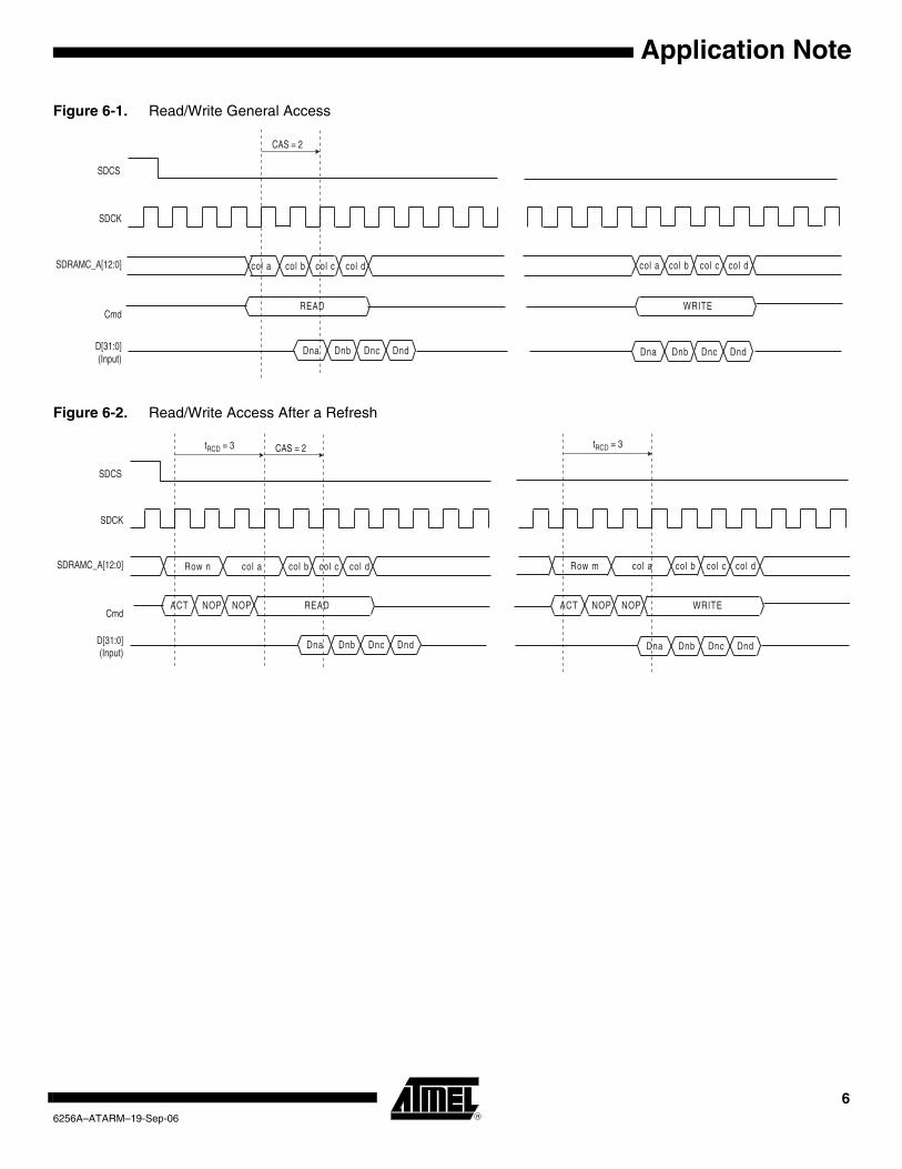
6.1 SDRAM Controller Write CycleThe SDRAM Controller allows burst access or single access. In both cases, the SDRAM control-ler keeps track of the active row in each bank, thus maximizing performance. To initiate a burstaccess, the SDRAM Controller uses the transfer type signal provided by the master requestingthe access. If the next access is a sequential write access, writing to the SDRAM device is car-ried out. If the next access is a sequential write access, but the current access is to a boundarypage, or if the next access is in another row, then the SDRAM Controller generates a prechargecommand, activates the new row and initiates a write command. To comply with SDRAM timingparameters, additional clock cycles are inserted between precharge/active (tRP) commands andactive/write (tRCD) commands.
6.2 SDRAM Controller Read CycleThe SDRAM Controller allows burst access or single access. In all cases, the SDRAM Controllerkeeps track of the active row in each bank, thus maximizing performance. If row and bankaddresses do not match the previous row/bank address, then the SDRAM controller automati-cally generates a precharge command, activates the new row and starts the read command. Tocomply with SDRAM timing parameters, additional clock cycles on SDCK are inserted betweenprecharge and active commands (tRP) and between active and read commands (tRCD). Thesetwo parameters are set in the configuration register of the SDRAM Controller. After a read com-mand, additional wait states are generated to comply with the CAS latency (1, 2 or 3 clockdelays specified in the configuration register).
6.3 Border ManagementWhen the memory row boundary has been reached, an automatic page break is inserted. In thiscase, the SDRAM controller generates a precharge command, activates the new row and ini-tiates a read or write command. To comply with SDRAM timing parameters, an additional clockcycle is inserted between the precharge/active (tRP) command and the active/read (tRCD)command.
56256A–ATARM–19-Sep-06
Application Note
Figure 6-1. Read/Write General Access
Figure 6-2. Read/Write Access After a Refresh
SDCK
SDCS
Cmd
SDRAMC_A[12:0]
D[31:0](Input)
col a col b col c col d
CAS = 2
Dna Dnb Dnc Dnd
col a col b col c col d
READ WRITE
Dna Dnb Dnc Dnd
SDCK
SDCS
Cmd
SDRAMC_A[12:0]
D[31:0](Input)
tRCD = 3
Row n col a col b col c col d
CAS = 2
Dna Dnb Dnc Dnd
Row m col a col b col c col d
tRCD = 3
ACT NOP NOP READ ACT NOP NOP WRITE
Dna Dnb Dnc Dnd
66256A–ATARM–19-Sep-06

Application Note
Figure 6-3. Read/Write Access After a Bank Opening
7. SDRAM Performance DefinitionThe SDRAM interface operates at system bus clock, up to a maximum frequency of 100 MHz.Using a 198 MHz AT91SAM9261 system as an example, the ARM926™ core runs at 198 MHz,the system bus operates at one-half the core frequency, thus the SDRAM interface operates at99 MHz.
The performance of the SDRAM interface is measured in throughput, which is the amount ofdata that can be transferred to and from the SDRAM in a given time period.
The throughput in bytes/second can be expressed by:
T = bytes/s or (bytes / cycles) * (cycles/s)
This depends on the SDRAM clock frequency (SDCK), the number of bytes per transfer (BPT)and the number of cycles. If the number of cycles per read and per write (CPR and CPW) are dif-ferent, this results in:
SDCK
SDCS
Cmd
SDRAMC_A[12:0]
D[31:0](Input)
tRCD = 3
Row n col a col b col c col d
CAS = 2
Dna Dnb Dnc Dnd
Row m col a col b col c col d
tRCD = 3
ACT NOP NOP READ
ACT NOP NOP WRITE
Dna Dnb Dnc Dnd
PRE NOP NOP
tRP = 3
PRE NOP NOP
tRP = 3
SDCK
SDCS
Cmd
SDRAMC_A[12:0]
D[31:0](Input)
76256A–ATARM–19-Sep-06

Application Note
• read contribution
TR = SDCK * BPT / CPR
• write contribution
TW = SDCK * BPT / CPW
Finally, let’s introduce a ratio of read and write (RR and RW), equal to the percentage ofaccesses that are reads and writes. In all cases, RR + WR must equal 1.0.
Formally, the SDRAM throughput (T) can be estimated by the sum of the amount of data trans-ferred by each mode (Read and Write) divided by the sum of access cycles, assuming SDRAMis doing nothing else during the delay:
T = (RR*TR*CPR + WR*TW*CPW) / (RR*CPR + WR*CPW)
Assuming the BPT is the same for reads and for writes:
T = SDCK * BPT * (RR + WR) / (RR*CPR + WR*CPW)
As RR + WR equals 1.0, finally:
T = SDCK * BPT / (RR*CPR + WR*CPW)
with:
• SDCK: The SDRAM Clock is the main factor in determining the SDRAM throughput. As all the accesses are paced by it, the higher the frequency of the SDRAM clock, the higher the SDRAM throughput.
• BPT: The SDRAM Controller allows burst access or single access. In all cases, the SDRAM Controller keeps track of the active row in each bank, thus maximizing performance of the SDRAM.
• Number of cycles per Read/Write
• CPR and CPW: The cycles per read CPR is CAS latency cycles + N cycles for burst of N words + 1 cycle for synchronizing with the internal system bus.
The cycles per write (CPW) equal N cycles for a burst of N words.
Additional cycles are included on memory boundary or after a refresh command.
• Ratio of Read and Write (RR and WR): This ratio depends on the application and can vary from 99-1% to 50-50%.
86256A–ATARM–19-Sep-06

Application Note
8. Influence of SDRAM Parameters
8.1 SDRAM Access Type
8.1.1 Single AccessSingle accesses occur when a single memory location is accessed per SDRAM access. If theaccess is a non-cached read, the access is the least efficient access possible.
8.1.2 Burst AccessSince the number of cycles to access SDRAM is pre-determined, the setup time cannot bereduced, but it can be amortized to minimize its impact. The higher the length of the burst, thehigher the SDRAM throughput.
In this typical case:
• SDCK is 99 MHz (cycles/second)
• Case 1: The number of bytes per transfer (BPT) is 32, corresponding to 8 words per transfer.
• Case 2: The number of bytes per transfer (BPT) is 4, corresponding to one single access.
• No memory boundary is reached, no Bank is to be opened.
• CAS is 2 (cycles), i.e., CPR is 11 (cycles) and CPW is 8 (cycles) for an 8-word burst access, CPR is 4 (cycles) and CPW is 1 (cycle) for a single access.
T1 = 99M * 32 / ((RR*11) + (WR*8))
T2 = 99M * 4 / ((RR*4) + (WR*1))
The user should avoid single accesses for best performance. In the rest of the document,Case 1 with an RR/WR of 50/50 is the reference.
8.2 SDRAM CASCAS can be 1, 2 or 3 cycles. As CAS are additional delays, an SDRAM device with a CASlatency of 1 yields better throughput than an SDRAM with a CAS latency of 3. The CAS latencyshould be selected depending on the operating frequency.
Under the same conditions, selecting an SDRAM device with a CAS latency of 3 means thatCPR is 12 (cycles) and CPW is 8 (cycles). Thus:
T = 99M * 32 / ((0.5*12) + (0.5*8)) = 316 Mbytes/s
A permanent throughput reduction by 16 Mbytes/s (5%) is relative to the CAS 2 SDRAM. Usingan SDRAM with a low CAS latency is desirable.
Table 8-1. Results for Different Application Cases
RR/WR 80/20 50/50 20/80
T1 (Mbytes/s) 305 333 368
T2 (Mbytes/s) 116 158 247
96256A–ATARM–19-Sep-06

Application Note
8.3 SDRAM RefreshesSDRAM requires periodic refreshes to ensure the integrity of the data arrays. During an SDRAMrefresh, accesses by the core are stalled until the refresh completes.
SDRAM requires periodic refresh of all rows every 64 milliseconds. For SDRAM devices with4096 rows, this gives a refresh cycle every 15.7 microseconds or 63,694 refreshes per second.
An auto-refresh command is used to refresh the SDRAM device. Refresh addresses are gener-ated internally by the SDRAM device and incremented after each auto-refresh automatically.The SDRAM Controller generates these auto-refresh commands periodically. An internal timer isloaded with the value in the register SDRAMC_TR that indicates the number of clock cyclesbetween refresh cycles.
An auto refresh phase typically requires 11 cycles (TRP + TRC), therefore:
63694 * 11 = 700,634 SDRAM clock cycles
are consumed each second by refreshes, which are not data accesses.
While the number is a small fraction of the available 99 MHz SDRAM clock cycles (0.7%), it doesrepresent a throughput reduction of nearly 2 Mbytes/second.
8.4 Bus Masters
8.4.1 ARM926EJ-S™
The ARM926EJ-S core includes additional address-synchronization cycles in the access. Thesecycles do not include the 1 cycle data bus synchronization.
Delays occur when performing initial access to memory due to cache overheads. These includecache lookup failure (potential MMU table walks), checks for write buffer draining, bus granting,etc.
Cached cores are designed to perform at their best when operating from the cache - there willalways be penalty cycles seen before accesses occur to external memory.
When the read is performed, a burst occurs on the bus and the data is read into ARM registers.For the subsequent write, the data is sent directly into the core’s write buffer; this drains in paral-lel with the core operation. If the subsequent operation is a read from external memory, then adelay occurs until the write buffer drain completes.
In summary, read and write actions mask the time for the write buffer to drain. A write saturatesthe buffer, and only a read can see the cache miss penalty for each LDM operation.
8.4.2 DMAA DMA can access the SDRAM without any additional cycles. The throughput is maximized.
8.5 SDRAM Memory BoundariesWhen the memory row boundary has been reached, the row is closed (PRECHARGE com-mand) before opening the new row. TRP and TRCD, which are 2 cycles long each, are to beadded, CPR is 14 (cycles) and CPW is 12 (cycles).
The throughput becomes:
T = 99M * 32 / ((0.5*15) + (0.5*12)) = 234 Mbytes/s
106256A–ATARM–19-Sep-06

Application Note
This event occurs each time a burst reaches a memory row boundary. In worst case, with anSDRAM page size of 255 bytes, this event occurs 8 / 255 = 3% of the time; 1.5% with anSDRAM page size of 512 bytes. Over time, the throughput reduction is about:
(333 - 234) * 3 % = 3.2 Mbytes/s = 0.9%
This influence is too small to be considered.
8.6 Conclusion To summarize the influence of SDRAM parameters:
• As the influence of the SDRAM clock is essential, it must be set appropriately.
• SDRAM CAS latency impacts the throughput. The CAS latency must be set to the lowest value matching the SDRAM frequency.
• SDRAM page size has no measurable influence.
• SDRAM refresh register should be set with an optimal value. A refresh delay shorter than necessary penalizes the throughput without any positive influence.
9. AT91SAM9261 SDRAM Controller Configuration
9.1 Initialization SequenceThe initialization sequence is generated by software. The SDRAM devices are initialized by thefollowing sequence:
1. SDRAM features must be set in the configuration register: asynchronous timings (TRC, TRAS, etc.), number of column, rows, CAS latency, and the data bus width.
2. The SDRAM memory type must be set in the Memory Device Register.
3. A minimum pause of 200 µs is provided to precede any signal toggle.
4. An All Banks Precharge command is issued to the SDRAM devices. The application must set Mode to 2 in the Mode Register and perform a write access to any SDRAM address.
5. Eight auto-refresh (CBR) cycles are provided. The application must set the Mode to 4 in the Mode Register and performs a write access to any SDRAM location height times.
6. A Mode Register set (MRS) cycle is issued to program the parameters of the SDRAM devices, in particular CAS latency and burst length. The application must set Mode to 3 in the Mode Register and perform a write access to the SDRAM. The write address must be chosen so that BA[1:0] are set to 0. For example, with a 16-bit 128 MB SDRAM (12 rows, 9 columns, 4 banks) bank address, the SDRAM write access should be done at the address 0x20000000.
7. The application must go into Normal Mode, setting Mode to 0 in the Mode Register and performing a write access at any location in the SDRAM.
8. Write the refresh rate into the count field in the SDRAMC Refresh Timer register. (Refresh rate = delay between refresh cycles). The SDRAM device requires a refresh every 15.625 us or 7.81 us. With a 100 MHz frequency, the Refresh Timer Counter Register must be set with the value 1562(15.652 is x 100 MHz) or 781(7.81 is x 100 MHz).
After initialization, the SDRAM devices are fully functional.
Initialization can only be carried out once.
116256A–ATARM–19-Sep-06
Application Note
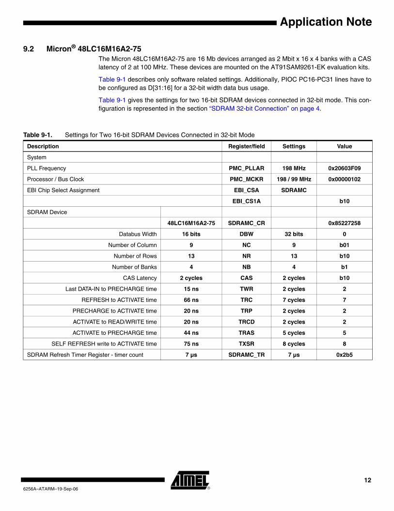
9.2 Micron® 48LC16M16A2-75The Micron 48LC16M16A2-75 are 16 Mb devices arranged as 2 Mbit x 16 x 4 banks with a CASlatency of 2 at 100 MHz. These devices are mounted on the AT91SAM9261-EK evaluation kits.
Table 9-1 describes only software related settings. Additionally, PIOC PC16-PC31 lines have tobe configured as D[31:16] for a 32-bit width data bus usage.
Table 9-1 gives the settings for two 16-bit SDRAM devices connected in 32-bit mode. This con-figuration is represented in the section “SDRAM 32-bit Connection” on page 4.
Table 9-1. Settings for Two 16-bit SDRAM Devices Connected in 32-bit Mode
Description Register/field Settings Value
System
PLL Frequency PMC_PLLAR 198 MHz 0x20603F09
Processor / Bus Clock PMC_MCKR 198 / 99 MHz 0x00000102
EBI Chip Select Assignment EBI_CSA SDRAMC
EBI_CS1A b10
SDRAM Device
48LC16M16A2-75 SDRAMC_CR 0x85227258
Databus Width 16 bits DBW 32 bits 0
Number of Column 9 NC 9 b01
Number of Rows 13 NR 13 b10
Number of Banks 4 NB 4 b1
CAS Latency 2 cycles CAS 2 cycles b10
Last DATA-IN to PRECHARGE time 15 ns TWR 2 cycles 2
REFRESH to ACTIVATE time 66 ns TRC 7 cycles 7
PRECHARGE to ACTIVATE time 20 ns TRP 2 cycles 2
ACTIVATE to READ/WRITE time 20 ns TRCD 2 cycles 2
ACTIVATE to PRECHARGE time 44 ns TRAS 5 cycles 5
SELF REFRESH write to ACTIVATE time 75 ns TXSR 8 cycles 8
SDRAM Refresh Timer Register - timer count 7 µs SDRAMC_TR 7 µs 0x2b5
126256A–ATARM–19-Sep-06

Application Note
9.3 Software ExampleThe code below is based on the Atmel libV3 definitions.
#include "AT91SAM9261.h"
#include "lib_AT91SAM9261.h"
#define AT91C_MASTER_CLOCK 100000000
#define AT91C_SDRAM ((volatile unsigned int *)0x20000000) /* Base address of the SDRAM */
//*--------------------------------------------------------------------------------------
//* Function Name : AT91F_InitSDRAM16
//* Object : Initialize the SDRAM in 16Bit mode
//* Input Parameters :
//* Output Parameters :
//*--------------------------------------------------------------------------------------
void AT91F_InitSDRAM16 (void)
{
/* Assign The CS1 to SDRAM function */
(*AT91C_MATRIX_EBICSA) |= AT91C_MATRIX_CS1A_SDRAMC;
/* Set the SDRAM features*/
*AT91C_SDRAMC_CR = AT91C_SDRAMC_NC_9 |
AT91C_SDRAMC_NR_13 |
AT91C_SDRAMC_CAS_2 |
AT91C_SDRAMC_NB_4_BANKS |
AT91C_SDRAMC_DBW_16_BITS |
AT91C_SDRAMC_TWR_2 |
AT91C_SDRAMC_TRC_7 |
AT91C_SDRAMC_TRP_2 |
AT91C_SDRAMC_TRCD_2 |
AT91C_SDRAMC_TRAS_5 |
AT91C_SDRAMC_TXSR_8 ;
/* Perform an All banks Precharge command */
*AT91C_SDRAMC_MR= 0x00000002;
*AT91C_SDRAM = 0;
/* Perform 8 auto-refresh (CBR) cycles*/ .
*AT91C_SDRAMC_MR= AT91C_SDRAMC_MODE_RFSH_CMD;
*AT91C_SDRAM = 0x00000000;
*AT91C_SDRAMC_MR= AT91C_SDRAMC_MODE_RFSH_CMD;
*AT91C_SDRAM = 0;
136256A–ATARM–19-Sep-06

Application Note
*AT91C_SDRAMC_MR= AT91C_SDRAMC_MODE_RFSH_CMD;
*AT91C_SDRAM = 0;
*AT91C_SDRAMC_MR= AT91C_SDRAMC_MODE_RFSH_CMD;
*AT91C_SDRAM = 0;
*AT91C_SDRAMC_MR= AT91C_SDRAMC_MODE_RFSH_CMD;
*AT91C_SDRAM = 0;
*AT91C_SDRAMC_MR= AT91C_SDRAMC_MODE_RFSH_CMD;
*AT91C_SDRAM = 0;
*AT91C_SDRAMC_MR= AT91C_SDRAMC_MODE_RFSH_CMD;
*AT91C_SDRAM = 0;
*AT91C_SDRAMC_MR= AT91C_SDRAMC_MODE_RFSH_CMD;
*AT91C_SDRAM = 0;
/* Perform a Mode Register set (MRS) cycle to program the parameters of the SDRAM devices*/
*AT91C_SDRAMC_MR= AT91C_SDRAMC_MODE_LMR_CMD;
*AT91C_SDRAM = 0;
/* Set refresh rate into the SDRAMC Refresh Timer register(7.8 µs)*/.
*AT91C_SDRAMC_TR= 780; /* 780 = AT91C_MASTER_CLOCK * 7.8µs */
/* Set Normal mode*/
*AT91C_SDRAMC_MR= AT91C_SDRAMC_MODE_NORMAL_CMD;
*AT91C_SDRAM = 0;
}
//*--------------------------------------------------------------------------------------
//* Function Name : AT91F_InitSDRAM32
//* Object : Initialize the SDRAM in 32bit mode
//* Input Parameters :
//* Output Parameters :
//*--------------------------------------------------------------------------------------
void AT91F_InitSDRAM32 (void)
{
/* Assign The CS1 to SDRAM function */
(*AT91C_MATRIX_EBICSA) |= AT91C_MATRIX_CS1A_SDRAMC;
/* Configure the PIO line multiplexed with the data[31:16] in peripheral mode*/
AT91F_SDRAMC_CfgPIO();
/* Set the SDRAM features*/
146256A–ATARM–19-Sep-06

Application Note
*AT91C_SDRAMC_CR = AT91C_SDRAMC_NC_9 |
AT91C_SDRAMC_NR_13 |
AT91C_SDRAMC_CAS_2 |
AT91C_SDRAMC_NB_4_BANKS |
AT91C_SDRAMC_DBW_32_BITS |
AT91C_SDRAMC_TWR_2 |
AT91C_SDRAMC_TRC_7 |
AT91C_SDRAMC_TRP_2 |
AT91C_SDRAMC_TRCD_2 |
AT91C_SDRAMC_TRAS_5 |
AT91C_SDRAMC_TXSR_8 ;
/* Perform an All banks Precharge command */
*AT91C_SDRAMC_MR= 0x00000002;
*AT91C_SDRAM = 0;
/* Perform 8 auto-refresh (CBR) cycles*/ .
*AT91C_SDRAMC_MR= AT91C_SDRAMC_MODE_RFSH_CMD;
*AT91C_SDRAM = 0;
*AT91C_SDRAMC_MR= AT91C_SDRAMC_MODE_RFSH_CMD;
*AT91C_SDRAM = 0;
*AT91C_SDRAMC_MR= AT91C_SDRAMC_MODE_RFSH_CMD;
*AT91C_SDRAM = 0;
*AT91C_SDRAMC_MR= AT91C_SDRAMC_MODE_RFSH_CMD;
*AT91C_SDRAM = 0;
*AT91C_SDRAMC_MR= AT91C_SDRAMC_MODE_RFSH_CMD;
*AT91C_SDRAM = 0;
*AT91C_SDRAMC_MR= AT91C_SDRAMC_MODE_RFSH_CMD;
*AT91C_SDRAM = 0;
*AT91C_SDRAMC_MR= AT91C_SDRAMC_MODE_RFSH_CMD;
*AT91C_SDRAM = 0;
*AT91C_SDRAMC_MR= AT91C_SDRAMC_MODE_RFSH_CMD;
*AT91C_SDRAM = 0;
/* Perform a Mode Register set (MRS) cycle to program the parameters of the SDRAM devices*/
*AT91C_SDRAMC_MR= AT91C_SDRAMC_MODE_LMR_CMD;
*AT91C_SDRAM = 0;
/* Set refresh rate into the SDRAMC Refresh Timer register(7.8 µs)*/.
156256A–ATARM–19-Sep-06

Application Note
*AT91C_SDRAMC_TR= 780; /* 780 = AT91C_MASTER_CLOCK * 7.8µs */
/* Set Normal mode*/
*AT91C_SDRAMC_MR= AT91C_SDRAMC_MODE_NORMAL_CMD;
*AT91C_SDRAM = 0;
}
9.4 ARM926EJ-S Access Results without MMUThe system is configured as described in Table 9-1, “Settings for Two 16-bit SDRAM DevicesConnected in 32-bit Mode,” on page 12. Only Icache is enabled to minimize the impact of codeexecution on measurements. The ARM Data Master is set as the fixed default master for theEBI.
The code copies 32 MBytes from 0x20000000 to 0x22000000 with different methods. Thismeans 64 Mbytes are transferred.
While SDCK is 99 MHz, one cycle corresponds to 10 ns in all the waveforms.
9.4.1 Single Access
9.4.1.1 DescriptionThe code performs read and write accesses of one word consecutively. Under these conditions,the ARM core adds 3 cycles between Write and Read and 6 cycles between Read and Write.These cycles include the code fetching in internal SRAM. This is the major effort of the ARMcore in this case.
Figure 9-1. SDRAM CAS Signal for a Single Access without MMU
The cycles per read (CPR) equal 2 CAS latency cycles + 1 cycle for 1 word + 6 cycles for theARM core + 1 cycle for bus synchronization.
The cycles per write (CPW) equal 1 cycle for a burst of 1 word + 3 cycles for the ARM core.
The RR equals WR.
Theoretically, the throughput equals:
166256A–ATARM–19-Sep-06

Application Note
T = 99M * 4 / (0.5*10 + 0.5*4) = 57 Mbytes/s
9.4.1.2 ResultThe 64 Mbytes are transferred in 1183 ms including code execution time. This gives a through-put of about 54 Mbytes/s.
9.4.2 4-word Burst Access
9.4.2.1 DescriptionThe code performs read and write accesses consecutively with 4-word long ldmia and stmiainstructions. Under these conditions, the ARM core adds 3 cycles between Write and Read and5 cycles between Read and Write. These cycles includes the code fetching in internal SRAM.
Figure 9-2. SDRAM CAS Signal for a 4-word Burst Access without MMU
The cycles per read (CPR) equal 2 CAS latency cycles + 4 cycles for a burst of 4 words + 5cycles for ARM core + 1 cycle for bus synchronization.
The cycles per write (CPW) equal 4 cycles for burst of 4 words + 3 cycles for ARM core.
The RR equals WR.
Theoretically, the thoughput equals:
T = 99M * 16 / (0.5*12 + 0.5*7) = 166 Mbytes/s
9.4.2.2 ResultThe 64 Mbytes are transferred in 422 ms including code execution time. This gives a throughputof about 152 Mbytes/s.
176256A–ATARM–19-Sep-06

Application Note
9.4.3 8-word Burst Access
9.4.3.1 DescriptionThe code performs read and write accesses consecutively with 8-word long ldmia and stmiainstructions. Under these conditions the ARM core adds 4 cycles between Write and Read and 5cycles between Read and Write. These cycles includes the code fetching in internal SRAM.
Figure 9-3. SDRAM CAS Signal for an 8-word Burst Access without MMU
The cycles per read (CPR) equal 2 CAS latency cycles + 8 cycles for burst of 8 words + 5 cyclesfor ARM core + 1 cycle for synchronization.
The cycles per write (CPW) equal 8 cycles for burst of 8 words + 4 cycles for ARM core.
The RR equals WR.
Theoretically, the thoughput equals:
T = 99M * 32 / (0.5*16 + 0.5*12) = 226 Mbytes/s
9.4.3.2 ResultThe 64 Mbytes are transferred in 295 ms including code execution time. This gives a thoughpuofabout 217 Mbytes/s.
186256A–ATARM–19-Sep-06

Application Note
9.5 ARM926EJ-S Accesses Results with MMUThe system is configured as described Table 9-1 on page 12. MMU, Icache and Dcache areenabled to optimize SDRAM accesses and minimize the impact of code execution on measure-ments. The ARM Data Master is set as the fixed default master for the EBI.
9.5.1 Single Access
9.5.1.1 DescriptionThe code performs read and write accesses of one word consecutively. With the MMU and theData Cache, the ARM core optimizes the access and performs a burst access to drain the writebuffer.
Figure 9-4. SDRAM CAS Signal for a Single Access with MMU
As it is difficult to separate Read and Write accesses, use the number of cycles for a 16-wordlong transfer (8 words are read and 8 words are write) as shown on the waveforms. Thus thenumber of cycles CPR + CPW + ARM core cycles is:
4 + 1 + 1 + 1 + 1 + 1 + 3 + 1 + 2 + 1 + 3 + 1 + 2 + 1 + 3 + 9 = 35.
Theoretically, the throughput equals:
T = 99M * 64 / 35 = 181 Mbytes/s
Result The 64 Mbytes are transferred in 369 ms including code execution time. This gives a throughputof about 173 Mbytes/s.
196256A–ATARM–19-Sep-06

Application Note
9.5.2 4-word Burst Access
9.5.2.1 DescriptionThe code performs read and write accesses consecutively with 4-word long ldmia and stmiainstructions. With the MMU and the Data Cache, the ARM core optimizes the access.
Figure 9-5. SDRAM CAS Signal for a 4-word Access with MMU
As it is difficult to separate Read and Write accesses, use the number of cycles for a 16-wordlong transfer (8 words are read and 8 words are write) as shown on the waveforms. Thus thenumber of cycle CPR + CPW + ARM core cycles is:
12 + 4 + 4 + 3 = 23
Theoretically, the throughput equals:
T = 99M * 64 / 23 = 275 Mbytes/s
9.5.2.2 ResultThe 64 Mbytes are transferred in 242 ms including code execution time. This gives a throughputof about 264 Mbytes/s.
206256A–ATARM–19-Sep-06

Application Note
9.5.3 8-word Burst Access
9.5.3.1 DescriptionThe code performs read and write accesses consecutively with 8-word long ldmia and stmiainstructions. With the MMU and the Data Cache, the ARM core optimizes the access and per-forms 16-word burst accesses.
Figure 9-6. SDRAM CAS Signal for a 8-word Access with MMU
As it is difficult to separate Read and Write accesses, use the number of cycles for a 16-wordlong transfer (8 words are read and 8 words are write) as shown on the waveforms. Thus thenumber of cycle CPR + CPW + ARM core cycles is:
16 + 7 = 23
Theoretically, the thoughput equals:
T = 99M * 64 / 23 = 275 Mbytes/s
9.5.3.2 ResultThe 64 Mbytes are transferred in 242 ms including code execution time. This gives a thoughputof about 264 Mbytes/s.
216256A–ATARM–19-Sep-06

Application Note
9.6 SDRAM Performance Conclusion
9.6.1 Theory versus Real LifeThe 5% difference between theory and measurement is due to the following factors, from mostimportant to the least important:
1. the ARM that executes code from the Instruction Cache. Notice the transfer time includes the code execution time
2. PRECHARGE command and Bank opening that are ignored in the theory
3. PIT accuracy of 1ms
9.6.2 Checklist
• As the SDRAM clock influence is essential, it must be set appropriately.
• SDRAM CAS latency impacts the thoughput. The CAS latency must be set to a value matching the SDRAM frequency.
• SDRAM page size has no measurable influence.
• SDRAM refresh register is to be set with an optimal value. A refresh delay shorter than necessary only penalizes the throughput without any positive influence.
• Software should take advantage of the SDRAM open-bank policy by locating code, data, etc. on separate SDRAM bank and row boundaries.
• Software should avoid single-beat accesses for best performance.
• Use MMU, Icache and Dcache as often as possible for best performance and minimum penalty in code running time.
• 8-word burst accesses are not necessary as the same results can be obtained with 4-word because of ARM optimization. 4-word accesses use fewer registers and are easier to manage by software.
• Software should attribute each Bus Master to an SDRAM Bank to save bank opening time, especially for high bandwidth peripherals such as the LCD DMA.
226256A–ATARM–19-Sep-06
Disclaimer: The information in this document is provided in connection with Atmel products. No license, express or implied, by estoppel or otherwise, to anyintellectual property right is granted by this document or in connection with the sale of Atmel products. EXCEPT AS SET FORTH IN ATMEL’S TERMS AND CONDI-TIONS OF SALE LOCATED ON ATMEL’S WEB SITE, ATMEL ASSUMES NO LIABILITY WHATSOEVER AND DISCLAIMS ANY EXPRESS, IMPLIED OR STATUTORYWARRANTY RELATING TO ITS PRODUCTS INCLUDING, BUT NOT LIMITED TO, THE IMPLIED WARRANTY OF MERCHANTABILITY, FITNESS FOR A PARTICULARPURPOSE, OR NON-INFRINGEMENT. IN NO EVENT SHALL ATMEL BE LIABLE FOR ANY DIRECT, INDIRECT, CONSEQUENTIAL, PUNITIVE, SPECIAL OR INCIDEN-TAL DAMAGES (INCLUDING, WITHOUT LIMITATION, DAMAGES FOR LOSS OF PROFITS, BUSINESS INTERRUPTION, OR LOSS OF INFORMATION) ARISING OUTOF THE USE OR INABILITY TO USE THIS DOCUMENT, EVEN IF ATMEL HAS BEEN ADVISED OF THE POSSIBILITY OF SUCH DAMAGES. Atmel makes norepresentations or warranties with respect to the accuracy or completeness of the contents of this document and reserves the right to make changes to specificationsand product descriptions at any time without notice. Atmel does not make any commitment to update the information contained herein. Unless specifically providedotherwise, Atmel products are not suitable for, and shall not be used in, automotive applications. Atmel’s products are not intended, authorized, or warranted for useas components in applications intended to support or sustain life.
Atmel Corporation Atmel Operations
2325 Orchard ParkwaySan Jose, CA 95131, USATel: 1(408) 441-0311Fax: 1(408) 487-2600
Regional Headquarters
EuropeAtmel SarlRoute des Arsenaux 41Case Postale 80CH-1705 FribourgSwitzerlandTel: (41) 26-426-5555Fax: (41) 26-426-5500
AsiaRoom 1219Chinachem Golden Plaza77 Mody Road TsimshatsuiEast KowloonHong KongTel: (852) 2721-9778Fax: (852) 2722-1369
Japan9F, Tonetsu Shinkawa Bldg.1-24-8 ShinkawaChuo-ku, Tokyo 104-0033JapanTel: (81) 3-3523-3551Fax: (81) 3-3523-7581
Memory2325 Orchard ParkwaySan Jose, CA 95131, USATel: 1(408) 441-0311Fax: 1(408) 436-4314
Microcontrollers2325 Orchard ParkwaySan Jose, CA 95131, USATel: 1(408) 441-0311Fax: 1(408) 436-4314
La ChantrerieBP 7060244306 Nantes Cedex 3, FranceTel: (33) 2-40-18-18-18Fax: (33) 2-40-18-19-60
ASIC/ASSP/Smart CardsZone Industrielle13106 Rousset Cedex, FranceTel: (33) 4-42-53-60-00Fax: (33) 4-42-53-60-01
1150 East Cheyenne Mtn. Blvd.Colorado Springs, CO 80906, USATel: 1(719) 576-3300Fax: 1(719) 540-1759
Scottish Enterprise Technology ParkMaxwell BuildingEast Kilbride G75 0QR, Scotland Tel: (44) 1355-803-000Fax: (44) 1355-242-743
RF/AutomotiveTheresienstrasse 2Postfach 353574025 Heilbronn, GermanyTel: (49) 71-31-67-0Fax: (49) 71-31-67-2340
1150 East Cheyenne Mtn. Blvd.Colorado Springs, CO 80906, USATel: 1(719) 576-3300Fax: 1(719) 540-1759
Biometrics/Imaging/Hi-Rel MPU/High-Speed Converters/RF Datacom
Avenue de RochepleineBP 12338521 Saint-Egreve Cedex, FranceTel: (33) 4-76-58-30-00Fax: (33) 4-76-58-34-80
Literature Requestswww.atmel.com/literature
6256A–ATARM–19-Sep-06
© 2006 Atmel Corporation. All rights reserved. Atmel®, logo and combinations thereof, Everywhere You Are® and others are registered trade-marks or trademarks of Atmel Corporation or its subsidiaries. ARM®, the ARMPowered® logo, Thumb® and others are registered trademarks ortrademarks of ARM Ltd. Other terms and product names may be trademarks of others.