Embed Size (px)
Citation preview
Using the SDRAM on Intel’sDE2-115 Board with Verilog Designs
For Quartus® Prime 18.1
1 Introduction
This tutorial explains how the SDRAM chips on the Intel® DE2-115 Development and Education board can beused with a Nios® II system implemented by using the Intel Platform Designer tool. The discussion is based on theassumption that the reader has access to a DE2-115 board and is familiar with the material in the tutorial Introductionto the Intel Platform Designer Tool.
The screen captures in the tutorial were obtained using the Quartus® Prime version 18.1; if other versions of thesoftware are used, some of the images may be slightly different.
Contents:
• Example Nios II System
• The SDRAM Interface
• Using the Platform Designer tool to Generate the Nios II System
• Integration of the Nios II System into the Quartus Prime Project
• Using the Clock Signals IP Core
Intel Corporation - FPGA University ProgramMarch 2019
1
USING THE SDRAM ON INTEL’S DE2-115 BOARD WITH VERILOG DESIGNS For Quartus® Prime 18.1
2 Background
The introductory tutorial Introduction to the Intel Platform Designer Tool explains how the memory in a Cyclone®
series FPGA chip can be used in the context of a simple Nios II system. For practical applications it is necessaryto have a much larger memory. The Intel DE2-115 board contains 2 SDRAM chips that can each store 64 Mbytesof data. Each chip is organized as 8M x 16 bits x 4 banks. The SDRAM chips require careful timing control. Toprovide access to the SDRAM chips, the Platform Designer tool implements an SDRAM Controller circuit. Thiscircuit generates the signals needed to deal with the SDRAM chips.
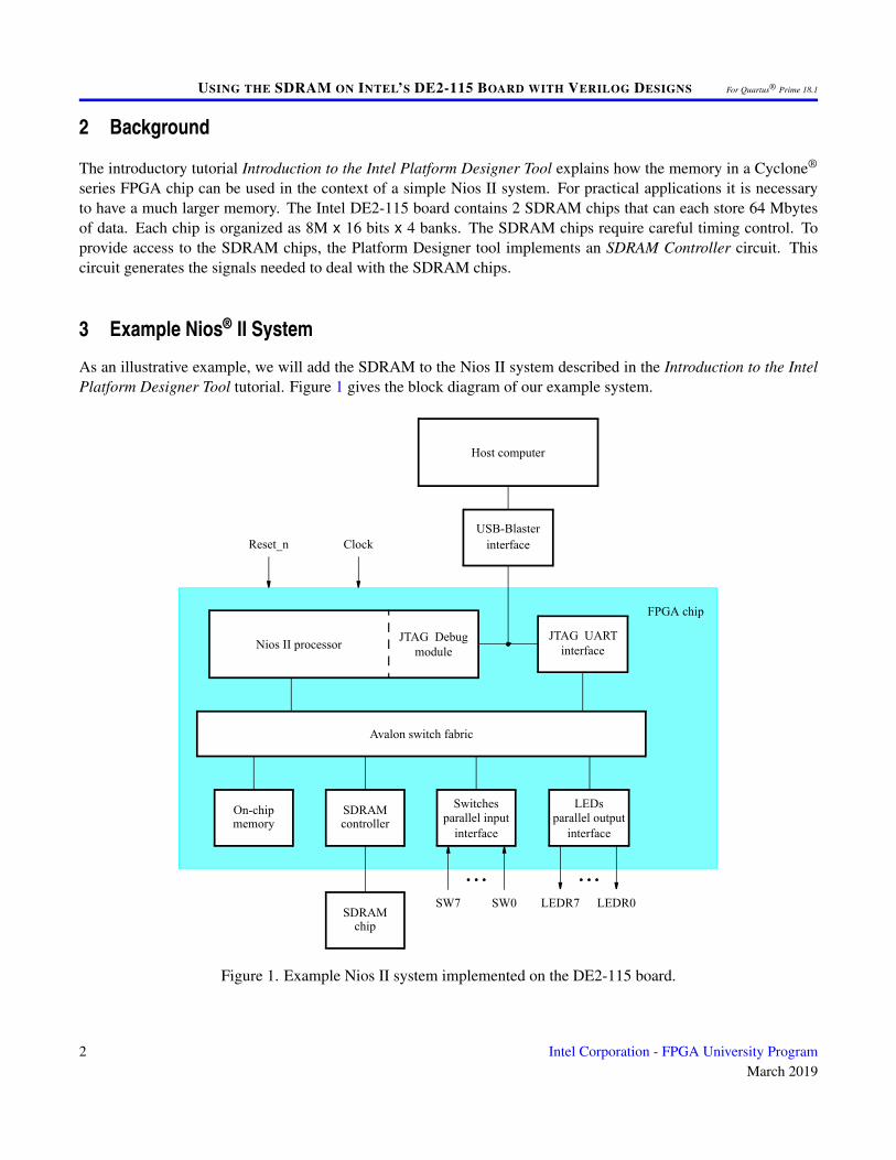
3 Example Nios® II System
As an illustrative example, we will add the SDRAM to the Nios II system described in the Introduction to the IntelPlatform Designer Tool tutorial. Figure 1 gives the block diagram of our example system.
On-chipmemory parallel input
interfaceparallel output
interface
Avalon switch fabric
JTAG UARTinterface
USB-Blasterinterface
Host computer
FPGA chip
SW7 SW0 LEDR7 LEDR0
Reset_n Clock
LEDsSwitchesSDRAMcontroller
SDRAMchip
Nios II processorJTAG Debug
module
Figure 1. Example Nios II system implemented on the DE2-115 board.
2 Intel Corporation - FPGA University ProgramMarch 2019
USING THE SDRAM ON INTEL’S DE2-115 BOARD WITH VERILOG DESIGNS For Quartus® Prime 18.1
The system realizes a trivial task. Eight toggle switches on the DE2-115 board, SW 7−0, are used to turn on or offthe eight green LEDs, LEDG7− 0. The switches are connected to the Nios II system by means of a parallel I/Ointerface configured to act as an input port. The LEDs are driven by the signals from another parallel I/O interfaceconfigured to act as an output port. To achieve the desired operation, the eight-bit pattern corresponding to the stateof the switches has to be sent to the output port to activate the LEDs. This will be done by having the Nios IIprocessor execute an application program. Continuous operation is required, such that as the switches are toggledthe lights change accordingly.
The introductory tutorial showed how we can use the Platform Designer tool to design the hardware needed toimplement this task, assuming that the application program which reads the state of the toggle switches and setsthe green LEDs accordingly is loaded into a memory block in the FPGA chip. In this tutorial, we will explain howSDRAM chips on the DE2-115 board can be included in the system in Figure 1, so that our application program canbe run from the SDRAM rather than from the on-chip memory.
Doing this tutorial, the reader will learn about:
• Using the Platform Designer tool to include an SDRAM interface for a Nios II-based system
• Timing issues with respect to the SDRAM on the DE2-115 board
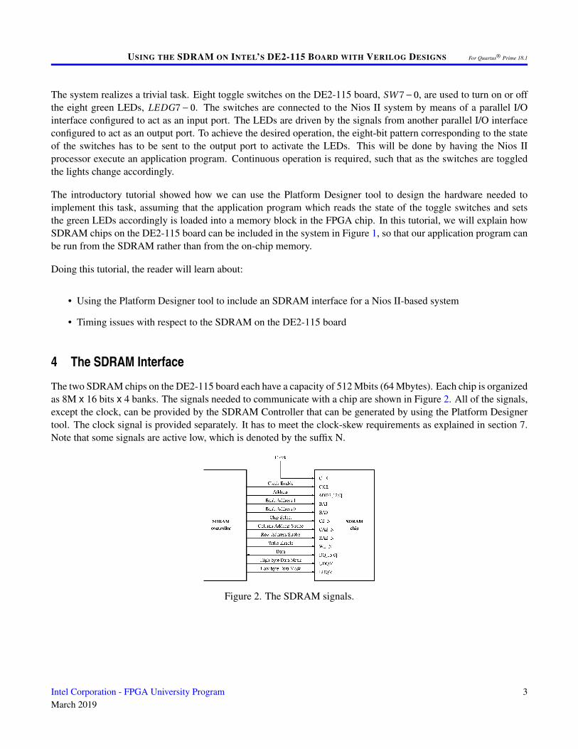
4 The SDRAM Interface
The two SDRAM chips on the DE2-115 board each have a capacity of 512 Mbits (64 Mbytes). Each chip is organizedas 8M x 16 bits x 4 banks. The signals needed to communicate with a chip are shown in Figure 2. All of the signals,except the clock, can be provided by the SDRAM Controller that can be generated by using the Platform Designertool. The clock signal is provided separately. It has to meet the clock-skew requirements as explained in section 7.Note that some signals are active low, which is denoted by the suffix N.
Figure 2. The SDRAM signals.
Intel Corporation - FPGA University ProgramMarch 2019
3
USING THE SDRAM ON INTEL’S DE2-115 BOARD WITH VERILOG DESIGNS For Quartus® Prime 18.1
5 Using the Platform Designer tool to Generate the Nios® II System
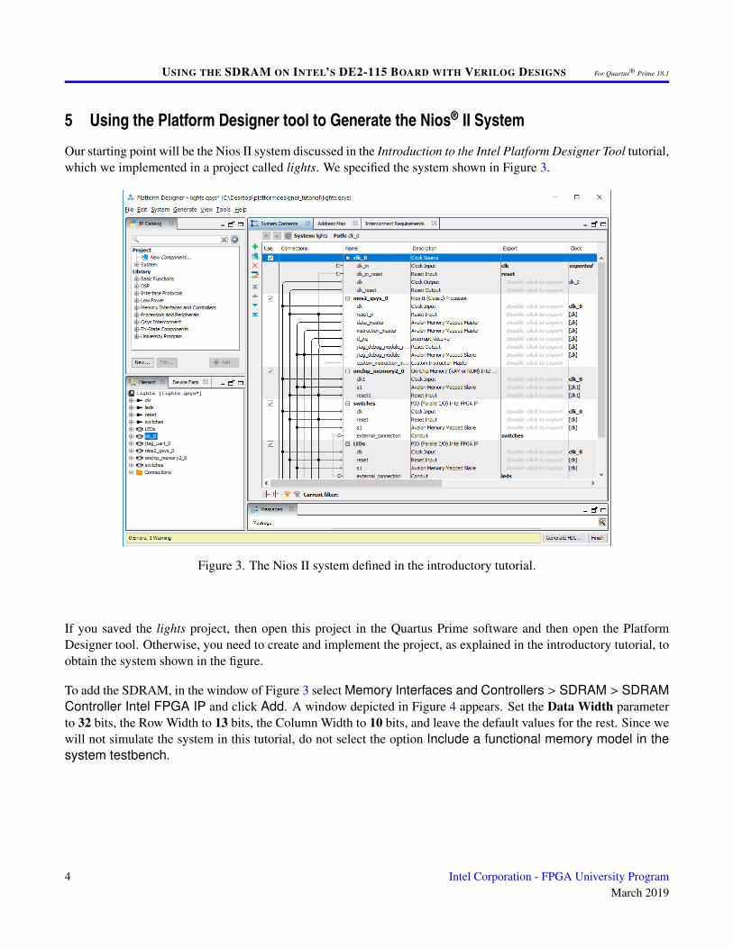
Our starting point will be the Nios II system discussed in the Introduction to the Intel Platform Designer Tool tutorial,which we implemented in a project called lights. We specified the system shown in Figure 3.
Figure 3. The Nios II system defined in the introductory tutorial.
If you saved the lights project, then open this project in the Quartus Prime software and then open the PlatformDesigner tool. Otherwise, you need to create and implement the project, as explained in the introductory tutorial, toobtain the system shown in the figure.
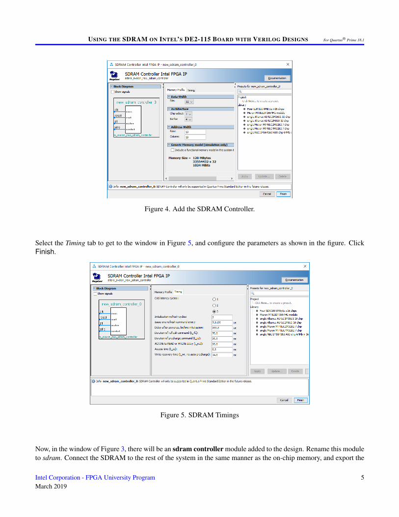
To add the SDRAM, in the window of Figure 3 select Memory Interfaces and Controllers > SDRAM > SDRAMController Intel FPGA IP and click Add. A window depicted in Figure 4 appears. Set the Data Width parameterto 32 bits, the Row Width to 13 bits, the Column Width to 10 bits, and leave the default values for the rest. Since wewill not simulate the system in this tutorial, do not select the option Include a functional memory model in thesystem testbench.
4 Intel Corporation - FPGA University ProgramMarch 2019
USING THE SDRAM ON INTEL’S DE2-115 BOARD WITH VERILOG DESIGNS For Quartus® Prime 18.1
Figure 4. Add the SDRAM Controller.
Select the Timing tab to get to the window in Figure 5, and configure the parameters as shown in the figure. ClickFinish.
Figure 5. SDRAM Timings
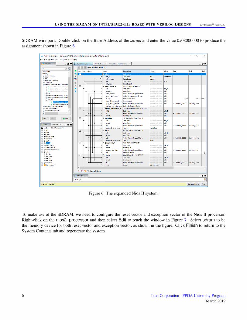
Now, in the window of Figure 3, there will be an sdram controller module added to the design. Rename this moduleto sdram. Connect the SDRAM to the rest of the system in the same manner as the on-chip memory, and export the
Intel Corporation - FPGA University ProgramMarch 2019
5
USING THE SDRAM ON INTEL’S DE2-115 BOARD WITH VERILOG DESIGNS For Quartus® Prime 18.1
SDRAM wire port. Double-click on the Base Address of the sdram and enter the value 0x08000000 to produce theassignment shown in Figure 6.
Figure 6. The expanded Nios II system.
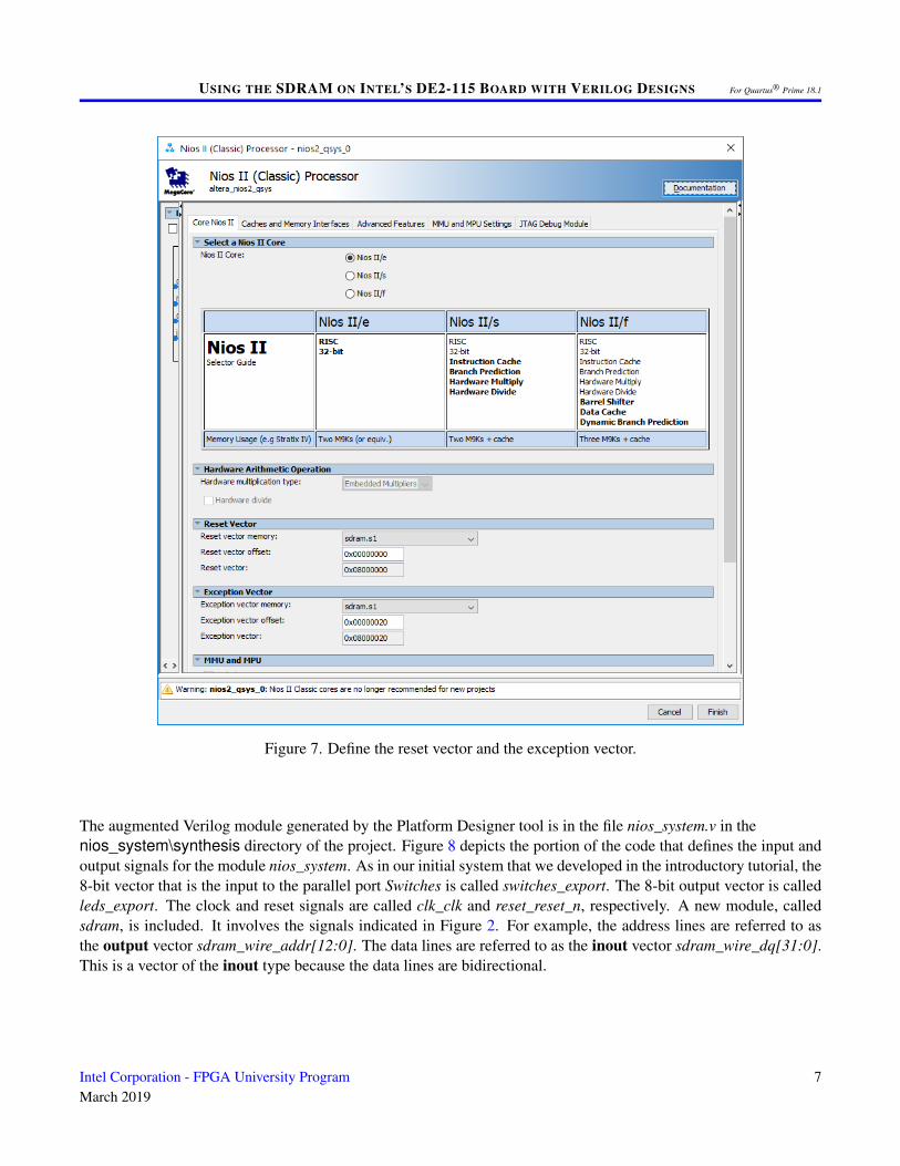
To make use of the SDRAM, we need to configure the reset vector and exception vector of the Nios II processor.Right-click on the nios2_processor and then select Edit to reach the window in Figure 7. Select sdram to bethe memory device for both reset vector and exception vector, as shown in the figure. Click Finish to return to theSystem Contents tab and regenerate the system.
6 Intel Corporation - FPGA University ProgramMarch 2019
USING THE SDRAM ON INTEL’S DE2-115 BOARD WITH VERILOG DESIGNS For Quartus® Prime 18.1
Figure 7. Define the reset vector and the exception vector.
The augmented Verilog module generated by the Platform Designer tool is in the file nios_system.v in thenios_system\synthesis directory of the project. Figure 8 depicts the portion of the code that defines the input andoutput signals for the module nios_system. As in our initial system that we developed in the introductory tutorial, the8-bit vector that is the input to the parallel port Switches is called switches_export. The 8-bit output vector is calledleds_export. The clock and reset signals are called clk_clk and reset_reset_n, respectively. A new module, calledsdram, is included. It involves the signals indicated in Figure 2. For example, the address lines are referred to asthe output vector sdram_wire_addr[12:0]. The data lines are referred to as the inout vector sdram_wire_dq[31:0].This is a vector of the inout type because the data lines are bidirectional.
Intel Corporation - FPGA University ProgramMarch 2019
7

USING THE SDRAM ON INTEL’S DE2-115 BOARD WITH VERILOG DESIGNS For Quartus® Prime 18.1
Figure 8. A part of the generated Verilog module.
6 Integration of the Nios® II System into the Quartus® Prime Project
Now, we have to instantiate the expanded Nios II system in the top-level Verilog module, as we have done in thetutorial Introduction to the Intel Platform Designer Tool. The module is named lights, because this is the name ofthe top-level design entity in our Quartus Prime project.
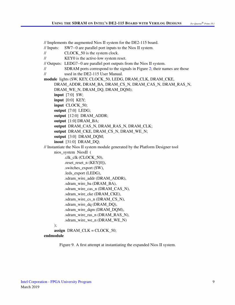
A first attempt at creating the new module is presented in Figure 9. The input and output ports of the module usethe pin names for the 50-MHz clock, CLOCK_50, pushbutton switches, KEY, toggle switches, SW, and green LEDs,LEDG, as used in our original design. They also use the pin names DRAM_CLK, DRAM_CKE, DRAM_ADDR,DRAM_BA, DRAM_CS_N, DRAM_CAS_N, DRAM_RAS_N, DRAM_WE_N, DRAM_DQ, and DRAM_DQM, whichcorrespond to the SDRAM signals indicated in Figure 2. All of these names are those specified in the DE2-115User Manual and included in the file called DE2_115.qsf, which can be found on Intel’s DE1-SoC web page athttps://www.altera.com/support/training/university/boards.html
Finally, note that we tried an obvious approach of using the 50-MHz system clock, CLOCK_50, as the clock signal,DRAM_CLK, for the SDRAM chips. This is specified by the assign statement in the code. This approach leads to apotential timing problem caused by the clock skew on the DE2-115 board, which can be fixed as explained in section7.
8 Intel Corporation - FPGA University ProgramMarch 2019
USING THE SDRAM ON INTEL’S DE2-115 BOARD WITH VERILOG DESIGNS For Quartus® Prime 18.1
// Implements the augmented Nios II system for the DE2-115 board.// Inputs: SW7−0 are parallel port inputs to the Nios II system.// CLOCK_50 is the system clock.// KEY0 is the active-low system reset.// Outputs: LEDG7−0 are parallel port outputs from the Nios II system.// SDRAM ports correspond to the signals in Figure 2; their names are those// used in the DE2-115 User Manual.module lights (SW, KEY, CLOCK_50, LEDG, DRAM_CLK, DRAM_CKE,
DRAM_ADDR, DRAM_BA, DRAM_CS_N, DRAM_CAS_N, DRAM_RAS_N,DRAM_WE_N, DRAM_DQ, DRAM_DQM);input [7:0] SW;input [0:0] KEY;input CLOCK_50;output [7:0] LEDG;output [12:0] DRAM_ADDR;output [1:0] DRAM_BA;output DRAM_CAS_N, DRAM_RAS_N, DRAM_CLK;output DRAM_CKE, DRAM_CS_N, DRAM_WE_N;output [3:0] DRAM_DQM;inout [31:0] DRAM_DQ;
// Instantiate the Nios II system module generated by the Platform Designer toolnios_system NiosII (
.clk_clk (CLOCK_50),
.reset_reset_n (KEY[0]),
.switches_export (SW),
.leds_export (LEDG),
.sdram_wire_addr (DRAM_ADDR),
.sdram_wire_ba (DRAM_BA),
.sdram_wire_cas_n (DRAM_CAS_N),
.sdram_wire_cke (DRAM_CKE),
.sdram_wire_cs_n (DRAM_CS_N),
.sdram_wire_dq (DRAM_DQ),
.sdram_wire_dqm (DRAM_DQM),
.sdram_wire_ras_n (DRAM_RAS_N),
.sdram_wire_we_n (DRAM_WE_N));assign DRAM_CLK = CLOCK_50;
endmodule
Figure 9. A first attempt at instantiating the expanded Nios II system.
Intel Corporation - FPGA University ProgramMarch 2019
9
USING THE SDRAM ON INTEL’S DE2-115 BOARD WITH VERILOG DESIGNS For Quartus® Prime 18.1
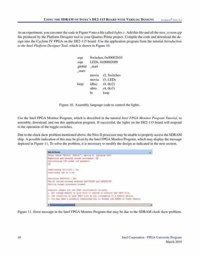
As an experiment, you can enter the code in Figure 9 into a file called lights.v. Add this file and all the nios_system.qipfile produced by the Platform Designer tool to your Quartus Prime project. Compile the code and download the de-sign into the Cyclone IV FPGA on the DE2-115 board. Use the application program from the tutorial Introductionto the Intel Platform Designer Tool, which is shown in Figure 10.
.equ Switches, 0x00002010
.equ LEDs, 0x00002000
.global _start_start:
movia r2, Switchesmovia r3, LEDs
loop: ldbio r4, 0(r2)stbio r4, 0(r3)br loop
Figure 10. Assembly language code to control the lights.
Use the Intel FPGA Monitor Program, which is described in the tutorial Intel FPGA Monitor Program Tutorial, toassemble, download, and run this application program. If successful, the lights on the DE2-115 board will respondto the operation of the toggle switches.
Due to the clock skew problem mentioned above, the Nios II processor may be unable to properly access the SDRAMchip. A possible indication of this may be given by the Intel FPGA Monitor Program, which may display the messagedepicted in Figure 11. To solve the problem, it is necessary to modify the design as indicated in the next section.
Figure 11. Error message in the Intel FPGA Monitor Program that may be due to the SDRAM clock skew problem.
10 Intel Corporation - FPGA University ProgramMarch 2019
USING THE SDRAM ON INTEL’S DE2-115 BOARD WITH VERILOG DESIGNS For Quartus® Prime 18.1
7 Using the Clock Signals IP Core
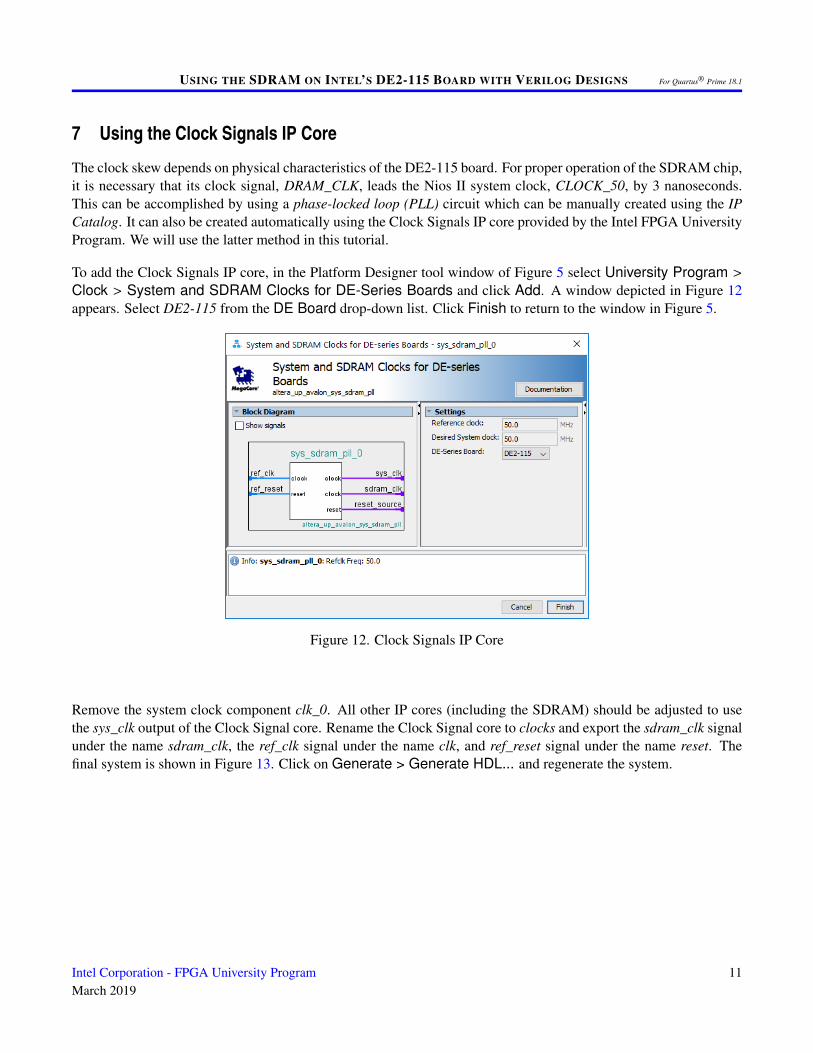
The clock skew depends on physical characteristics of the DE2-115 board. For proper operation of the SDRAM chip,it is necessary that its clock signal, DRAM_CLK, leads the Nios II system clock, CLOCK_50, by 3 nanoseconds.This can be accomplished by using a phase-locked loop (PLL) circuit which can be manually created using the IPCatalog. It can also be created automatically using the Clock Signals IP core provided by the Intel FPGA UniversityProgram. We will use the latter method in this tutorial.
To add the Clock Signals IP core, in the Platform Designer tool window of Figure 5 select University Program >Clock > System and SDRAM Clocks for DE-Series Boards and click Add. A window depicted in Figure 12appears. Select DE2-115 from the DE Board drop-down list. Click Finish to return to the window in Figure 5.
Figure 12. Clock Signals IP Core
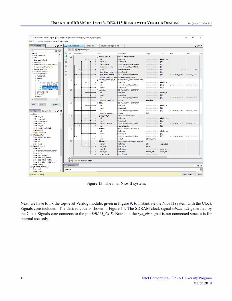
Remove the system clock component clk_0. All other IP cores (including the SDRAM) should be adjusted to usethe sys_clk output of the Clock Signal core. Rename the Clock Signal core to clocks and export the sdram_clk signalunder the name sdram_clk, the ref_clk signal under the name clk, and ref_reset signal under the name reset. Thefinal system is shown in Figure 13. Click on Generate > Generate HDL... and regenerate the system.
Intel Corporation - FPGA University ProgramMarch 2019
11
USING THE SDRAM ON INTEL’S DE2-115 BOARD WITH VERILOG DESIGNS For Quartus® Prime 18.1
Figure 13. The final Nios II system.
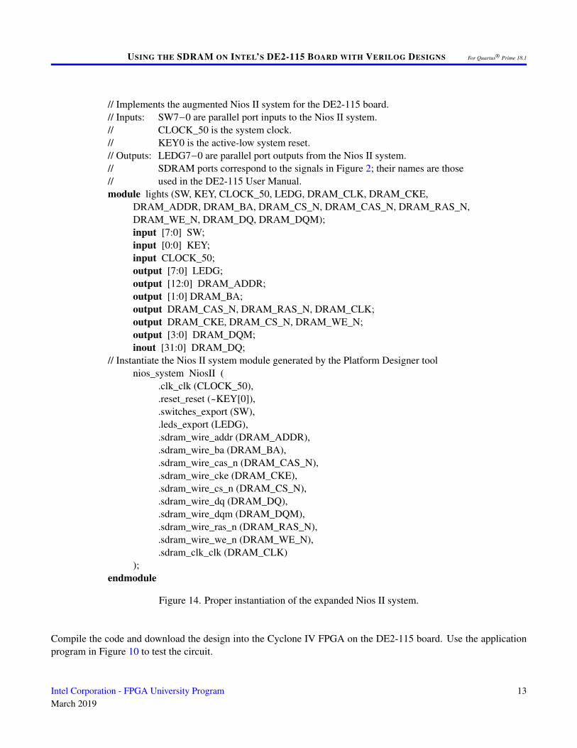
Next, we have to fix the top-level Verilog module, given in Figure 9, to instantiate the Nios II system with the ClockSignals core included. The desired code is shown in Figure 14. The SDRAM clock signal sdram_clk generated bythe Clock Signals core connects to the pin DRAM_CLK. Note that the sys_clk signal is not connected since it is forinternal use only.
12 Intel Corporation - FPGA University ProgramMarch 2019
USING THE SDRAM ON INTEL’S DE2-115 BOARD WITH VERILOG DESIGNS For Quartus® Prime 18.1
// Implements the augmented Nios II system for the DE2-115 board.// Inputs: SW7−0 are parallel port inputs to the Nios II system.// CLOCK_50 is the system clock.// KEY0 is the active-low system reset.// Outputs: LEDG7−0 are parallel port outputs from the Nios II system.// SDRAM ports correspond to the signals in Figure 2; their names are those// used in the DE2-115 User Manual.module lights (SW, KEY, CLOCK_50, LEDG, DRAM_CLK, DRAM_CKE,
DRAM_ADDR, DRAM_BA, DRAM_CS_N, DRAM_CAS_N, DRAM_RAS_N,DRAM_WE_N, DRAM_DQ, DRAM_DQM);input [7:0] SW;input [0:0] KEY;input CLOCK_50;output [7:0] LEDG;output [12:0] DRAM_ADDR;output [1:0] DRAM_BA;output DRAM_CAS_N, DRAM_RAS_N, DRAM_CLK;output DRAM_CKE, DRAM_CS_N, DRAM_WE_N;output [3:0] DRAM_DQM;inout [31:0] DRAM_DQ;
// Instantiate the Nios II system module generated by the Platform Designer toolnios_system NiosII (
.clk_clk (CLOCK_50),
.reset_reset (~KEY[0]),
.switches_export (SW),
.leds_export (LEDG),
.sdram_wire_addr (DRAM_ADDR),
.sdram_wire_ba (DRAM_BA),
.sdram_wire_cas_n (DRAM_CAS_N),
.sdram_wire_cke (DRAM_CKE),
.sdram_wire_cs_n (DRAM_CS_N),
.sdram_wire_dq (DRAM_DQ),
.sdram_wire_dqm (DRAM_DQM),
.sdram_wire_ras_n (DRAM_RAS_N),
.sdram_wire_we_n (DRAM_WE_N),
.sdram_clk_clk (DRAM_CLK));
endmodule
Figure 14. Proper instantiation of the expanded Nios II system.
Compile the code and download the design into the Cyclone IV FPGA on the DE2-115 board. Use the applicationprogram in Figure 10 to test the circuit.
Intel Corporation - FPGA University ProgramMarch 2019
13

USING THE SDRAM ON INTEL’S DE2-115 BOARD WITH VERILOG DESIGNS For Quartus® Prime 18.1
Copyright © Intel Corporation. All rights reserved. Intel, the Intel logo, Altera, Arria, Avalon, Cyclone, Enpirion,MAX, Nios, Quartus and Stratix words and logos are trademarks of Intel Corporation or its subsidiaries in the U.S.and/or other countries. Intel warrants performance of its FPGA and semiconductor products to current specificationsin accordance with Intel’s standard warranty, but reserves the right to make changes to any products and servicesat any time without notice. Intel assumes no responsibility or liability arising out of the application or use of anyinformation, product, or service described herein except as expressly agreed to in writing by Intel. Intel customersare advised to obtain the latest version of device specifications before relying on any published information andbefore placing orders for products or services.
*Other names and brands may be claimed as the property of others.
14 Intel Corporation - FPGA University ProgramMarch 2019