Embed Size (px)
Citation preview
644 OPTICS LETTERS / Vol. 20, No. 6 / March 15, 1995
Variable optical delay line based on a birefringentplanar optical platform
Masayasu Yamaguchi and Katsuhiko Hirabayashi
NTT Network Service Systems Laboratories, 3-9-11 Midori-cho, Musashino-shi, Tokyo, 180 Japan
Received August 18, 1994
A variable optical delay line is proposed for accurately adjusting optical signal timing in photonic systems. Thisdelay line is based on a birefringent planar optical platform characterized by the multiple reflection of light beams.It consists of a birefringent plate, ly4 plates, mirrors, and a liquid-crystal layer. It can select an arbitrary delayfrom a set of discrete delays precisely determined by the thickness of the birefringent plate. A feasibility studyconfirms seven-step delay line operation with a 240-ps unit delay.
Variable or programmable optical delay lines can beused as buffer memories or timing adjusters in pho-tonic systems. Fiber-based buffer memories havebeen studied for photonic asynchronous transfermode switching systems.1 – 4 The unit delay timeof these buffer memories is determined by the celllength and ranges from tens to hundreds of nanosec-onds. On the other hand, timing adjusters are usedfor adjusting optical signal propagation delay forsynchronization in photonic systems. The unit de-lay time is much shorter (e.g., from tens to hundredsof picoseconds) than that of the buffer memories.However, such short delay times cannot easily beobtained in fiber delay lines because the fiber mustbe made too short to be set accurately during fabrica-tion. Therefore, conventional experimental systemshave employed mechanical optical delay lines in-stead of fiber-based ones as timing adjusters. Themechanical delay lines are based on the adjustmentof an air gap (optical path length in free space) be-tween the fiber collimators. These mechanical delaylines, however, have some drawbacks; they are notcompact, and the delay switching speed is low.
In this Letter we propose a new variable optical de-lay line based on a birefringent planar optical plat-form and a liquid-crystal (LC) cell. It is compact andcan change delays within 100 ms to 100 ms. We alsoreport the results of an experimental delay line as afeasibility study.
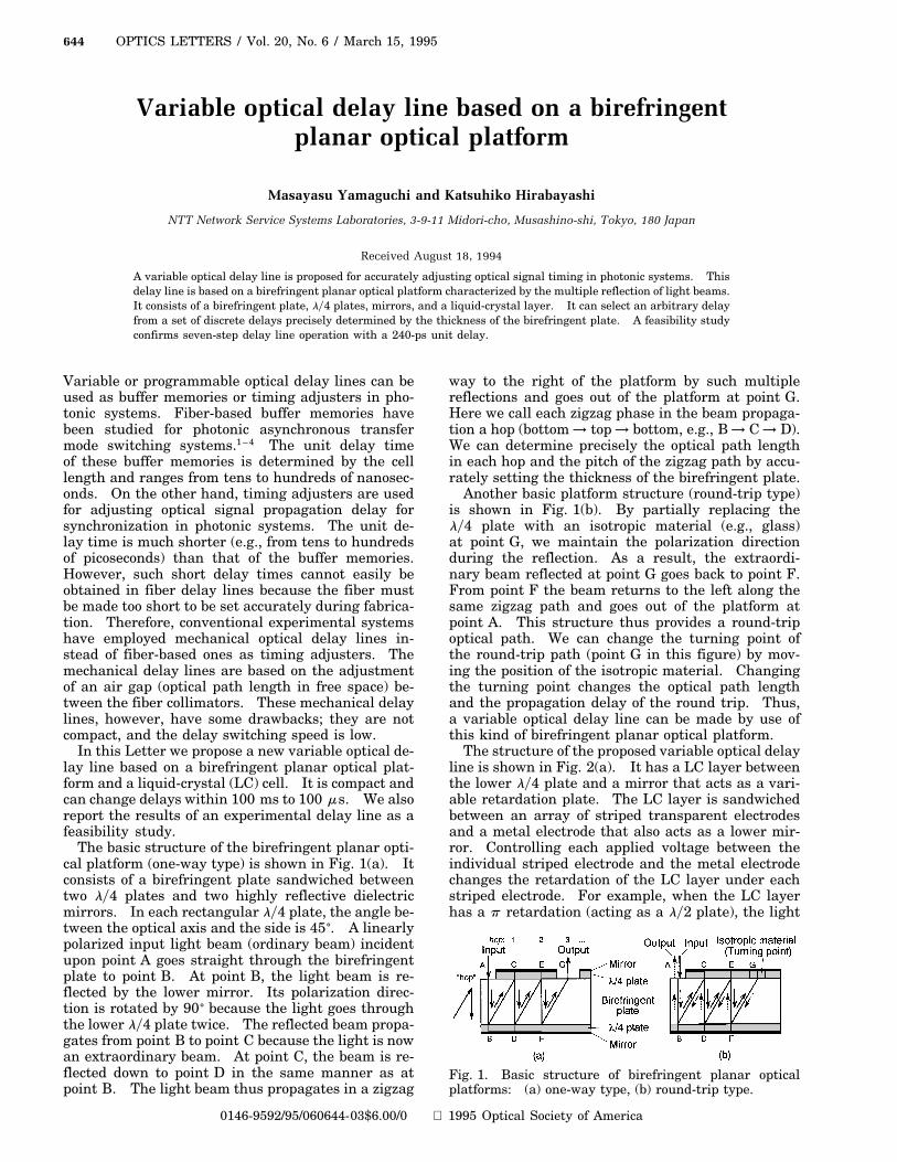
The basic structure of the birefringent planar opti-cal platform (one-way type) is shown in Fig. 1(a). Itconsists of a birefringent plate sandwiched betweentwo ly4 plates and two highly reflective dielectricmirrors. In each rectangular ly4 plate, the angle be-tween the optical axis and the side is 45±. A linearlypolarized input light beam (ordinary beam) incidentupon point A goes straight through the birefringentplate to point B. At point B, the light beam is re-flected by the lower mirror. Its polarization direc-tion is rotated by 90± because the light goes throughthe lower ly4 plate twice. The reflected beam propa-gates from point B to point C because the light is nowan extraordinary beam. At point C, the beam is re-flected down to point D in the same manner as atpoint B. The light beam thus propagates in a zigzag
0146-9592/95/060644-03$6.00/0
way to the right of the platform by such multiplereflections and goes out of the platform at point G.Here we call each zigzag phase in the beam propaga-tion a hop (bottom ! top ! bottom, e.g., B ! C ! D).We can determine precisely the optical path lengthin each hop and the pitch of the zigzag path by accu-rately setting the thickness of the birefringent plate.
Another basic platform structure (round-trip type)is shown in Fig. 1(b). By partially replacing thely4 plate with an isotropic material (e.g., glass)at point G, we maintain the polarization directionduring the reflection. As a result, the extraordi-nary beam reflected at point G goes back to point F.From point F the beam returns to the left along thesame zigzag path and goes out of the platform atpoint A. This structure thus provides a round-tripoptical path. We can change the turning point ofthe round-trip path (point G in this figure) by mov-ing the position of the isotropic material. Changingthe turning point changes the optical path lengthand the propagation delay of the round trip. Thus,a variable optical delay line can be made by use ofthis kind of birefringent planar optical platform.
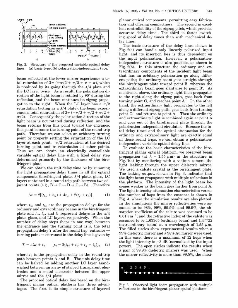
The structure of the proposed variable optical delayline is shown in Fig. 2(a). It has a LC layer betweenthe lower ly4 plate and a mirror that acts as a vari-able retardation plate. The LC layer is sandwichedbetween an array of striped transparent electrodesand a metal electrode that also acts as a lower mir-ror. Controlling each applied voltage between theindividual striped electrode and the metal electrodechanges the retardation of the LC layer under eachstriped electrode. For example, when the LC layerhas a p retardation (acting as a ly2 plate), the light
Fig. 1. Basic structure of birefringent planar opticalplatforms: (a) one-way type, (b) round-trip type.
1995 Optical Society of America
March 15, 1995 / Vol. 20, No. 6 / OPTICS LETTERS 645
Fig. 2. Structure of the proposed variable optical delaylines: (a) basic type, (b) polarization-independent type.
beam reflected at the lower mirror experiences a to-tal retardation of 3p (py2 1 py2 1 p 1 p), whichis produced by its going through the ly4 plate andthe LC layer twice. As a result, the polarization di-rection of the light beam is rotated by 90± during thereflection, and the beam continues its zigzag propa-gation to the right. When the LC layer has a py2retardation (acting as a ly4 plate), the beam experi-ences a total retardation of 2p (py2 1 py2 1 py2 1py2). Consequently the polarization direction of thelight beam is not rotated during reflection, and thebeam returns from this point toward the entrance;this point becomes the turning point of the round-trippath. Therefore we can select an arbitrary turningpoint by properly setting the retardation of the LClayer at each point: py2 retardation at the desiredturning point and p retardation at other points.Thus we can obtain an electrically controllablevariable optical delay line with a fixed delay stepdetermined primarily by the thickness of the bire-fringent plate.
We can obtain the unit delay time Dt by summingthe light propagation delay times in all the opticalcomponents (birefringent plate, ly4 plate, glass, LClayer) contained in a round-trip path between two ad-jacent points (e.g., B ! C ! D ! C ! B). Therefore
Dt 2fstbo 1 tbed 1 4tw 1 2stg 1 tLdg , (1)
where tbo and tbe are the propagation delays for theordinary and extraordinary beams in the birefringentplate and tw, tg, and tL represent delays in the ly4plate, glass, and LC layers, respectively. When thenumber of delay steps (hops in one way) betweenthe entrance and the turning point is s, the totalpropagation delay T after the round trip (entrance !turning point ! entrance) in the delay line is given by
T sDt 1 t0 ft0 2stbo 1 tw 1 tg 1 tLdg , (2)
where t0 is the propagation delay in the round-trippath between points A and B. The unit delay timecan be halved by adding another LC layer (sand-wiched between an array of striped transparent elec-trodes and a metal electrode) between the uppermirror and the ly4 plate.
The proposed optical delay line based on the bire-fringent planar optical platform has three advan-tages. The first is its simple structure of layered
planar optical components, permitting easy fabrica-tion and offering compactness. The second is excel-lent controllability of the zigzag pitch, which providesaccurate delay time. The third is faster switch-ing speed of delay times than with mechanical de-lay lines.
The basic structure of the delay lines shown inFig. 2(a) can handle only linearly polarized inputlight, and its insertion loss is thus dependent onthe input polarization. However, a polarization-independent structure is also possible, as shown inFig. 2(b). In this structure the ordinary and ex-traordinary components of the incident light beamthat has an arbitrary polarization go along differ-ent paths; the ordinary beam goes straight throughthe birefringent plate toward point B, whereas theextraordinary beam goes slantwise to point B0. Asmentioned above, the ordinary light then propagatesto the right along the zigzag path, goes back fromturning point G, and reaches point A. On the otherhand, the extraordinary light propagates to the leftalong a different zigzag path, goes back from turningpoint G0, and returns to point A. Then the ordinaryand extraordinary light is combined again at point Aand goes out of the birefringent plate through thepolarization-independent circulator. Because the to-tal delay times and the optical attenuation for theordinary and extraordinary light are exactly equalin these round trips, we can obtain a polarization-independent variable optical delay line.
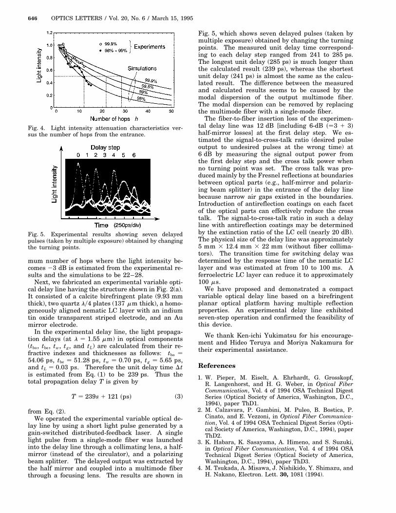
To evaluate the basic characteristics of the bire-fringent planar optical platform, we observed beampropagation (at l 1.55 mm) in the structure inFig. 1(a) by monitoring with a vidicon camera thelight leaking through the upper dielectric mirror.We used a calcite crystal as the birefringent plate.The leaking output, shown in Fig. 3, indicates thatthe light beam propagates with multiple reflections inthe platform. The intensity of the light beam be-comes weaker as the beam goes farther from point A.The light intensity attenuation characteristics versusthe number of hops from the entrance is shown inFig. 4, where the simulation results are also plotted.In the simulations the mirror reflectivities were as-sumed to be 98%, 99%, 99.5%, and 99.9%, the ab-sorption coefficient of the calcite was assumed to be0.01 cm21, and the refractive index of the calcite wasassumed to be 1.63365 (ordinary beam) and 1.47722(extraordinary beam) at a wavelength of 1.55 mm.The filled circles show experimental results when a99% dielectric mirror and a 98% Au mirror were used.In this case, there is a maximum of 12 hops whenthe light intensity is 23 dB (normalized by the inputpower). The open circles indicate the results whena pair of 99.9% dielectric mirrors was used. Whenthe mirror reflectivity is more than 99.5%, the maxi-
Fig. 3. Observed light beam propagation with multiplereflections in the birefringent planar optical platform.
646 OPTICS LETTERS / Vol. 20, No. 6 / March 15, 1995
Fig. 4. Light intensity attenuation characteristics ver-sus the number of hops from the entrance.
Fig. 5. Experimental results showing seven delayedpulses (taken by multiple exposure) obtained by changingthe turning points.
mum number of hops where the light intensity be-comes 23 dB is estimated from the experimental re-sults and the simulations to be 22–28.
Next, we fabricated an experimental variable opti-cal delay line having the structure shown in Fig. 2(a).It consisted of a calcite birefringent plate (9.93 mmthick), two quartz ly4 plates (137 mm thick), a homo-geneously aligned nematic LC layer with an indiumtin oxide transparent striped electrode, and an Aumirror electrode.
In the experimental delay line, the light propaga-tion delays (at l 1.55 mm) in optical components(tbo, tbe, tw, tg, and tL) are calculated from their re-fractive indexes and thicknesses as follows: tbo 54.06 ps, tbe 51.28 ps, tw 0.70 ps, tg 5.65 ps,and tL 0.03 ps. Therefore the unit delay time Dtis estimated from Eq. (1) to be 239 ps. Thus thetotal propagation delay T is given by
T 239s 1 121 spsd (3)
from Eq. (2).We operated the experimental variable optical de-
lay line by using a short light pulse generated by again-switched distributed-feedback laser. A singlelight pulse from a single-mode fiber was launchedinto the delay line through a collimating lens, a half-mirror (instead of the circulator), and a polarizingbeam splitter. The delayed output was extracted bythe half mirror and coupled into a multimode fiberthrough a focusing lens. The results are shown in
Fig. 5, which shows seven delayed pulses (taken bymultiple exposure) obtained by changing the turningpoints. The measured unit delay time correspond-ing to each delay step ranged from 241 to 285 ps.The longest unit delay (285 ps) is much longer thanthe calculated result (239 ps), whereas the shortestunit delay (241 ps) is almost the same as the calcu-lated result. The difference between the measuredand calculated results seems to be caused by themodal dispersion of the output multimode fiber.The modal dispersion can be removed by replacingthe multimode fiber with a single-mode fiber.
The fiber-to-fiber insertion loss of the experimen-tal delay line was 12 dB [including 6-dB s3 1 3dhalf-mirror losses] at the first delay step. We es-timated the signal-to-cross-talk ratio (desired pulseoutput to undesired pulses at the wrong time) at6 dB by measuring the signal output power fromthe first delay step and the cross talk power whenno turning point was set. The cross talk was pro-duced mainly by the Fresnel reflections at boundariesbetween optical parts (e.g., half-mirror and polariz-ing beam splitter) in the entrance of the delay linebecause narrow air gaps existed in the boundaries.Introduction of antireflection coatings on each facetof the optical parts can effectively reduce the crosstalk. The signal-to-cross-talk ratio in such a delayline with antireflection coatings may be determinedby the extinction ratio of the LC cell (nearly 20 dB).The physical size of the delay line was approximately5 mm 3 12.4 mm 3 22 mm (without fiber collima-tors). The transition time for switching delay wasdetermined by the response time of the nematic LClayer and was estimated at from 10 to 100 ms. Aferroelectric LC layer can reduce it to approximately100 ms.
We have proposed and demonstrated a compactvariable optical delay line based on a birefringentplanar optical platform having multiple reflectionproperties. An experimental delay line exhibitedseven-step operation and confirmed the feasibility ofthis device.
We thank Ken-ichi Yukimatsu for his encourage-ment and Hideo Teruya and Moriya Nakamura fortheir experimental assistance.
References
1. W. Pieper, M. Eiselt, A. Ehrhardt, G. Grosskopf,R. Langenhorst, and H. G. Weber, in Optical FiberCommunication, Vol. 4 of 1994 OSA Technical DigestSeries (Optical Society of America, Washington, D.C.,1994), paper ThD1.
2. M. Calzavara, P. Gambini, M. Puleo, B. Bostica, P.Cinato, and E. Vezzoni, in Optical Fiber Communica-tion, Vol. 4 of 1994 OSA Technical Digest Series (Opti-cal Society of America, Washington, D.C., 1994), paperThD2.
3. K. Habara, K. Sasayama, A. Himeno, and S. Suzuki,in Optical Fiber Communication, Vol. 4 of 1994 OSATechnical Digest Series (Optical Society of America,Washington, D.C., 1994), paper ThD3.
4. M. Tsukada, A. Misawa, J. Nishikido, Y. Shimazu, andH. Nakano, Electron. Lett. 30, 1081 (1994).