Embed Size (px)
Citation preview

Vertically integrated metal-clad/silicon dioxide-shell microtube arrays for high-spatial-resolution light stimuli in salineM. Sakata, T. Nakamura, T. Matsuo, A. Goryu, M. Ishida, and T. Kawano
Citation: Applied Physics Letters 104, 164101 (2014); doi: 10.1063/1.4871710 View online: http://dx.doi.org/10.1063/1.4871710 View Table of Contents: http://scitation.aip.org/content/aip/journal/apl/104/16?ver=pdfcov Published by the AIP Publishing Articles you may be interested in The role of group index engineering in series-connected photonic crystal microcavities for high density sensormicroarrays Appl. Phys. Lett. 104, 141103 (2014); 10.1063/1.4871012 Optical loss in silicon microphotonic waveguides induced by metallic contamination Appl. Phys. Lett. 92, 131108 (2008); 10.1063/1.2903714 Optical improvement of photonic devices fabricated by Ga + focused ion beam micromachining J. Vac. Sci. Technol. B 25, 1609 (2007); 10.1116/1.2770741 Microfabricated Sr Ti O 3 ridge waveguides Appl. Phys. Lett. 86, 221106 (2005); 10.1063/1.1942634 Inductively coupled plasma etching for arrayed waveguide gratings fabrication in silica on silicon technology J. Vac. Sci. Technol. B 20, 2085 (2002); 10.1116/1.1510528
This article is copyrighted as indicated in the article. Reuse of AIP content is subject to the terms at: http://scitation.aip.org/termsconditions. Downloaded to IP: 133.15.22.53
On: Tue, 22 Apr 2014 00:20:18
Vertically integrated metal-clad/silicon dioxide-shell microtube arraysfor high-spatial-resolution light stimuli in saline
M. Sakata,1 T. Nakamura,1 T. Matsuo,1 A. Goryu,1,2 M. Ishida,1,3 and T. Kawano1,a)
1Department of Electrical and Electronic Information Engineering, Toyohashi University of Technology,Toyohashi, Aichi 441-8580, Japan2Japan Society for the Promotion of Science (JSPS), Chiyoda, Tokyo 102-0083, Japan3Electronics-Interdisciplinary Research Institute (EIIRIS), Toyohashi University of Technology,Toyohashi, Aichi 441-8580, Japan
(Received 14 January 2014; accepted 6 April 2014; published online 21 April 2014)
Microdevices composed of integrated microscale light source arrays are powerful tools in optogenetic
applications. Herein, we prepared vertically aligned 3-lm inner diameter silicon dioxide (SiO2)
tube-based optical light waveguide arrays. To increase the locality of the light stimuli through the
tube, we also fabricated metal-cladded SiO2 tubes using iridium (Ir). After filling the tube with a saline
solution, the saline-core/Ir-clad/SiO2-shell waveguide exhibited light stimuli without spreading. With
a 532-nm wavelength, the half-power width of the light intensity measured 10lm above the tube tip
was 3 lm, while that of the saline/SiO2-shell waveguide was 9.6 lm, which was more than three
times wider. Such high-spatial-resolution optical light stimuli will offer a new class of optogenetic
applications, including light stimuli for specific regions of a neuron (e.g., axons or dendrites).VC 2014 AIP Publishing LLC. [http://dx.doi.org/10.1063/1.4871710]
Compared to conventional electrophysiological meth-
ods, optogenetics,1 which combines optical and genetics
methods (e.g., neuronal activations with channelrhodopsin-
22 or inhabitation with halorhodopsin), offers a higher spa-
tiotemporal resolution for in vivo/in vitro measurements of
neurons/cells. Microdevices that consist of both microscale
light sources and microelectrode arrays have been fabricated;
these devices exhibit simultaneous optical stimulation and
electrical recording of neurons/cells.3,4 To date, none have
demonstrated optical and electrical measurements of neuro-
ns/cells using the same alignment within a tissue, although
these types of high-spatial-resolution measurements will
offer a new class of optogenetics, such as light stimuli and
electrical recordings for specific regions of a neuron (e.g.,
axons or dendrites).5 Additionally, it is currently infeasible
to fabricate an array of vertical microscale-diameter needle-
like waveguides via a standard microfabrication process.
The limitations of conventional microdevices in optoge-
netics can be overcome by fabricating a vertical tube-like
waveguide array. We have fabricated vertically aligned
high-aspect-ratio tube arrays of silicon dioxide (SiO2),6,7 and
have demonstrated drug delivery6 and electrical recording7
capabilities using sub-5-lm diameter SiO2 tube arrays.
These microtubes may realize “multifunctional” measure-
ments of neurons/cells in the same alignment.
Here, we show the light stimulating capabilities of a
SiO2 microtube for optogenetic applications with a high spa-
tial resolution. With a light source, including fibers and
microscale light emitting diodes (LEDs), placed at the base
of the tube, optical signals through the SiO2 tube can be used
for light stimuli (Fig. 1(a)). However, passing through a SiO2
tube may decrease the locality of the light stimuli and
increase the optical crosstalk between the tubes. These per-
formance issues can be addressed by considering the
material of the tube waveguide, such as a high index material
like the core or a metal as the clad.8,9 To realize a high spa-
tial resolution of optical light stimuli through a SiO2 tube,
herein we fabricate metal-clad/SiO2-shell microtube arrays
(Fig. 1(c)). Such high-spatial-resolution optical stimuli can
be used for specific regions of a neuron (e.g., axons or den-
drites). Although the metal-clad causes optical transmission
loss, increasing the input power of the light source (fibers or
LEDs) can realize light stimuli with sufficient intensity for
optogenetic applications. In the device design, the optical
propagation in a saline-filled metal/SiO2 microtube is calcu-
lated using the finite-difference time-domain (FDTD)
method. The effects of the metal clad on the performance of
the light stimuli are discussed by comparing to a SiO2 tube
with a same geometry.
The metal layer formed inside a SiO2 tube acts as the clad
for the SiO2 tube-based waveguide, and using a metal with a
smaller resistivity as the clad material increases the optical effi-
ciency.8,9 Here, we used Ir (electrical resistivity¼ 4.71� 10�9
X�m at 20 �C) as the clad material because the Ir inside the
SiO2 tube increases the stiffness of the tube (Young’s moduli
of SiO2 and Ir are 75 GPa and 528 GPa, respectively), improv-
ing the penetration capability of the tube into a tissue. The
other advantage is that Ir has low electrolyte/metal interfacial
electrical impedance characteristics. Such a low impedance
material formed inside the tube decreases the impedance of a
saline-filled tube with a high output/input signal amplitude
ratio in electrical recordings of neurons/cells.7,10 The penetra-
tion and neural recording capabilities of the Ir-clad/SiO2-shell
microtube will be discussed in the future.
Optical propagation in a saline/SiO2 or saline/Ir/SiO2
tube can be analyzed by the FDTD method (Figs. 1(b) and
1(d)). To compare the optical properties between two tubes
with the same geometry, the thicknesses of the SiO2 shell
and inside Ir-clad layer of the Ir/SiO2 tube were set to
800 nm and 200 nm, respectively (total thickness¼ 1 lm)a)Email: [email protected]. Tel.: þ81(532)-44-6738
0003-6951/2014/104(16)/164101/5/$30.00 VC 2014 AIP Publishing LLC104, 164101-1
APPLIED PHYSICS LETTERS 104, 164101 (2014)
This article is copyrighted as indicated in the article. Reuse of AIP content is subject to the terms at: http://scitation.aip.org/termsconditions. Downloaded to IP: 133.15.22.53
On: Tue, 22 Apr 2014 00:20:18
(Fig. 1(d)), while the wall thickness of the SiO2 tube was
1 lm (Fig. 1(b)). To realize a tube with a low invasiveness
during tissue penetration,11,12 herein the common tube inner
diameter was set at 3 lm. The tube length was set at 20 lm,
which is sufficient to penetrate numerous thin biological
samples, including brain slices (tens to hundreds of microns)
and retinae (�200 lm).3,13
For optogenetic applications, we analyzed the optical
propagations of each tube using wavelengths of 470 nm for
channelrhodopsin-2 and 580 nm for halorhodopsin. Optical
propagation using 532-nm wavelength has been used for appli-
cations of light stimuli to retinae (e.g., mouse retina3 and gold
fish retina13). Figures 1(b) and 1(d) show the transverse electric
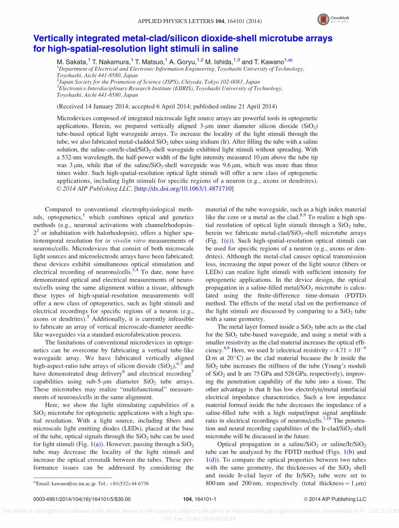
(TE) simulations performed for saline/SiO2 and saline/Ir/SiO2
tubes, respectively. The Ir-clad layer improves the locality of
light stimuli compared to that of a SiO2 tube. Note that the
refractive indices of SiO2 (nSiO2), Ir (nIr), and saline solution
(nsaline) varied with wavelength [470 nm (nSiO2¼ 1.551,
nIr¼ 1.887þ 3.809i, and nsaline¼ 1.336), 532 nm (nSiO2
¼ 1.547, nIr¼ 2.145þ 4.222i, and nsaline¼ 1.334), and 580 nm
(nSiO2¼ 1.545, nIr¼ 2.357þ 4.441i, and nsaline¼ 1.333)]. All
the light sources modeled in the calculation were plane waves,
which represent a laser through an optical fiber placed at the
bottom of each tube.
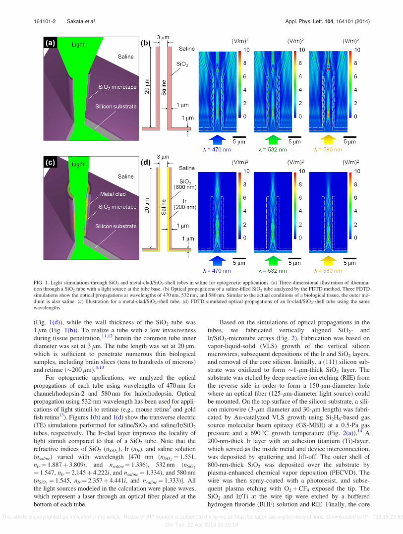
Based on the simulations of optical propagations in the
tubes, we fabricated vertically aligned SiO2- and
Ir/SiO2-microtube arrays (Fig. 2). Fabrication was based on
vapor-liquid-solid (VLS) growth of the vertical silicon
microwires, subsequent depositions of the Ir and SiO2 layers,
and removal of the core silicon. Initially, a (111) silicon sub-
strate was oxidized to form �1-lm-thick SiO2 layer. The
substrate was etched by deep reactive ion etching (RIE) from
the reverse side in order to form a 150-lm-diameter hole
where an optical fiber (125-lm-diameter light source) could
be mounted. On the top surface of the silicon substrate, a sili-
con microwire (3-lm diameter and 30-lm length) was fabri-
cated by Au-catalyzed VLS growth using Si2H6-based gas
source molecular beam epitaxy (GS-MBE) at a 0.5-Pa gas
pressure and a 690 �C growth temperature (Fig. 2(a)).14 A
200-nm-thick Ir layer with an adhesion titanium (Ti)-layer,
which served as the inside metal and device interconnection,
was deposited by sputtering and lift-off. The outer shell of
800-nm-thick SiO2 was deposited over the substrate by
plasma-enhanced chemical vapor deposition (PECVD). The
wire was then spray-coated with a photoresist, and subse-
quent plasma etching with O2þCF4 exposed the tip. The
SiO2 and Ir/Ti at the wire tip were etched by a buffered
hydrogen fluoride (BHF) solution and RIE. Finally, the core
FIG. 1. Light stimulations through SiO2 and metal-clad/SiO2-shell tubes in saline for optogenetic applications. (a) Three-dimensional illustration of illumina-
tion through a SiO2 tube with a light source at the tube base. (b) Optical propagations of a saline-filled SiO2 tube analyzed by the FDTD method. Three FDTD
simulations show the optical propagations at wavelengths of 470 nm, 532 nm, and 580 nm. Similar to the actual conditions of a biological tissue, the outer me-
dium is also saline. (c) Illustration for a metal-clad/SiO2-shell tube. (d) FDTD simulated optical propagations of an Ir-clad/SiO2-shell tube using the same
wavelengths.
164101-2 Sakata et al. Appl. Phys. Lett. 104, 164101 (2014)
This article is copyrighted as indicated in the article. Reuse of AIP content is subject to the terms at: http://scitation.aip.org/termsconditions. Downloaded to IP: 133.15.22.53
On: Tue, 22 Apr 2014 00:20:18
silicon wire was etched by XeF2 gas until the tube was con-
nected with the hole on the reverse side. Figure 2(c) shows a
SEM image of a fabricated Ir/SiO2 microtube with inner
and outer diameters of 3 and 4 lm, respectively. By simply
pattering the Ir/Ti layers as an interconnection, each Ir/SiO2
microtube could be connected with the device-bonding
pad for future applications of multisite electrical recordings
of neurons/cells (Fig. 2(d)).7 To compare the optical
properties, SiO2 tubes with the same inner and outer diame-
ters were also fabricated by eliminating metal depositions
(Fig. 2(b)).6,7
Optical transmissions through the fabricated SiO2 and
Ir/SiO2 microtubes were characterized in saline solutions.
Herein, the laser light source of an individual tube was an
optical fiber (125-lm diameter) mounted on the reverse side
of the substrate through a guide, and the optical signal
through the tube was detected using a CCD camera mounted
over the tube (Figs. 3(a), 3(b), 3(d), and 3(e)). The wave-
length of the laser for the optical transmission tests was
532 nm because this wavelength is suitable for future appli-
cations of optical stimuli to retinae.3,13 The transmission rate
of each tube was obtained by measuring the output/input
powers with and without placing the tube device between the
detector and the fiber, while the common focal point of the
detector was set 10 lm above the tube tip. The power of the
laser without the microtube device was 2.0 mW. The
saline/Ir/SiO2 tube exhibited a transmission rate of 0.097%
(Figs. 3(d) and 3(e)), while the saline/SiO2 tube with the
same geometry exhibited a transmission rate of 0.11% (Figs.
3(a) and 3(b)). Although the transmission rate of the
saline/Ir/SiO2 tube was less than that of the saline/SiO2 tube
due to absorption in the Ir metal clad,8,9 the intensity of the
light stimuli increased as the input power of the light source
increased. The optical transmission tests also indicated that
the area of light stimulation through the saline/Ir/SiO2 tube
was smaller than that of the SiO2 tube; these stimulation
areas were further examined.
The effect of the Ir clad on the locality of the light
stimuli was characterized using the half-power width, which
represents the spatial distribution of light at a 50% intensity.
Figs. 3(c) and 3(f) show the distributions of the light
intensities through saline/SiO2 and saline/Ir/SiO2 tubes,
FIG. 2. Fabrication process for both vertical SiO2- and Ir-clad/SiO2-shell microtubes. (a) SEM image of a VLS grown silicon microwire. (b) SEM image of a
SiO2 microtube fabricated by deposition of SiO2 over a silicon wire, exposing the tip section, and etching the core silicon. Inner and outer diameters of a fabri-
cated SiO2 tube are 3 lm and 4 lm, respectively. Tube length is 24 lm. (c) SEM image of an Ir-clad/SiO2-shell microtube, which is fabricated by adding Ir/Ti
depositions to the fabrication process of SiO2 tube (b). The fabricated Ir/SiO2 tube exhibits the same inner and outer diameters (3 lm and 4 lm). Tube length is
19 lm. (d) SEM image of an array of Ir/SiO2 tubes integrated with interconnections of Ir/Ti. Red square in the SEM is consistent with the tube shown in (c).
Each tube is spaced 500-lm apart.
164101-3 Sakata et al. Appl. Phys. Lett. 104, 164101 (2014)
This article is copyrighted as indicated in the article. Reuse of AIP content is subject to the terms at: http://scitation.aip.org/termsconditions. Downloaded to IP: 133.15.22.53
On: Tue, 22 Apr 2014 00:20:18
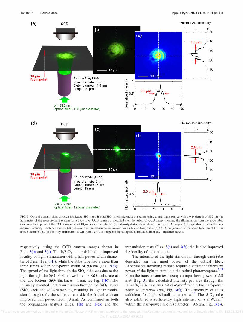
respectively, using the CCD camera images shown in
Figs. 3(b) and 3(e). The Ir/SiO2 tube exhibited an improved
locality of light stimulation with a half-power-width diame-
ter of 3 lm (Fig. 3(f)), while the SiO2 tube had a more than
three times wider half-power width of 9.6 lm (Fig. 3(c)).
The spread of the light through the SiO2 tube was due to the
light through the SiO2 shell as well as the SiO2 substrate at
the tube bottom (SiO2 thickness¼ 1 lm, see Fig. 1(b)). The
Ir layer prevented light transmission through the SiO2 layers
(SiO2 shell and SiO2 substrate), resulting in light transmis-
sion through only the saline-core inside the Ir-clad with an
improved half-power-width (3 lm). As confirmed in both
the propagation analysis (Figs. 1(b) and 1(d)) and the
transmission tests (Figs. 3(c) and 3(f)), the Ir clad improved
the locality of light stimuli.
The intensity of the light stimulation through each tube
depended on the input power of the optical fiber.
Experiments involving retinae require a sufficient intensity/
power of the light to stimulate the retinal photoreceptors.3,13
From the transmission tests using an input laser power of 2.0
mW (Fig. 3), the calculated intensity per area through the
saline/Ir/SiO2 tube was 69 mW/mm2 within the half-power
width (diameter¼ 3 lm, Fig. 3(f)). This intensity value is
sufficient for light stimuli to a retina.13 The SiO2 tube
also exhibited a sufficiently high intensity of 8 mW/mm2
within the half-power width (diameter¼ 9.6 lm, Fig. 3(c)).
FIG. 3. Optical transmissions through fabricated SiO2- and Ir-clad/SiO2-shell microtubes in saline using a laser light source with a wavelength of 532 nm. (a)
Schematic of the measurement system for a SiO2 tube. CCD camera is mounted over the tube. (b) CCD image showing the illumination from the SiO2 tube.
Common focal point of the CCD camera is set 10 lm above the tube tip. (c) Intensity distribution taken from the CCD image (b). Image also includes the nor-
malized intensity—distance curves. (d) Schematic of the measurement system for an Ir clad/SiO2 tube. (e) CCD image taken at the same focal point (10 lm
above the tube tip). (f) Intensity distribution taken from the CCD image (e) including the normalized intensity—distance curves.
164101-4 Sakata et al. Appl. Phys. Lett. 104, 164101 (2014)
This article is copyrighted as indicated in the article. Reuse of AIP content is subject to the terms at: http://scitation.aip.org/termsconditions. Downloaded to IP: 133.15.22.53
On: Tue, 22 Apr 2014 00:20:18
Although the 532-nm wavelength is suitable for transmission
tests in future retinal experiments, the wavelength of the
light source (e.g., 470 nm and 580 nm) can be varied for
optogenetic applications. Because light sources, including
fibers and microscale LEDs, can be set at the base of each
tube, numerous wavelengths and input powers can be real-
ized for optogenetic applications.
The fabricated tubes exhibited surface roughness
because the films were deposited over the VLS grown
silicon-wires with facets (�100 nm in roughness). The afore-
mentioned propagation analyses (Figs. 1(b) and 1(d))
employed smooth surface models of SiO2- and Ir/SiO2-tubes.
The rough surface of the each tube may reduce the intensity
of the light stimuli compared to that of the analysis due to
the additional transmission loss associated with the scatter-
ing at a rough surface (Fig. 3). One way to reduce the surface
roughness of the tubes is to use a VLS silicon-wire with a
smooth surface, which can be obtained by thermal annealing
in hydrogen for an as-VLS grown silicon-wire.15
In summary, we designed and fabricated vertically
aligned microscale-diameter SiO2- and Ir/SiO2-tube arrays,
and discussed their light stimulation capabilities for optoge-
netic applications. A comparison between the two types of
tubes using FDTD simulations and transmission tests con-
firmed that the locality of light stimuli is improved through a
saline/Ir/SiO2 tube. Such high-spatial-resolution optical light
stimuli to neurons/cells should realize a new class of optoge-
netic applications (e.g., light stimuli with a microscale spot
area in specific regions of a neuron, such as dendrites and
axons). In addition, the Ir clad can reduce the electrode im-
pedance inside the SiO2 tube during electrophysiological
recordings,7 providing optical and electrical measurements
of neurons/cells in the same alignment.
The authors would like to thank Professor Tetsuhiro
Harimoto, Professor Hirohito Sawahata, and Professor Rika
Numano for their fruitful discussions, Mitsuaki Ashiki and
Hiroyuki Takase for their assistance with the fabrication proc-
esses, and members at Wakahara Laboratory at Toyohashi
Tech for their help with the optical measurements. This work
was supported by Grants-in-Aid for Scientific Research (S),
Young Scientists (B), and the PRESTO Program from JST.
A. Goryu is a recipient of a JSPS fellowship.
1F. Zhang, A. M. Aravanis, A. Adamantidis, L. Lecea, and K. Deisseroth,
Nat. Rev. Neurosci. 8, 577 (2007).2G. Nage, T. Szellas, W. Huhn, S. Kateriya, N. Adeishvili, P. Berthold, D.
Ollig, P. Hegemann, and E. Bamberg, PNAS 100, 13940 (2003).3J. Zhang, F. Laiwalla, J. A. Kim, H. Urabe, R. V. Wagenen, Y. K. Song,
B. W. Connors, F. Zhang, K. Deisseroth, and A. V. Nurmikko, J. Neural
Eng. 6, 055007 (2009).4N. Grossman, V. Poher, M. S. Grubb, G. T. Kennedy, K. Nikolic, B.
McGovern, R. B. Palmini, Z. Gong, E. M. Drakakis, M. A. A. Neil, M. D.
Dawson, J. Burrone, and P. Degenaar, J. Neural Eng. 7, 016004 (2010).5A. M. Packer, D. S. Peterka, J. J. Hirtz, R. Prakash, K. Deisseroth, and R.
Yuste, Nat. Methods 9, 1202 (2012).6K. Takei, T. Kawashima, T. Kawano, H. Kaneko, K. Sawada, and
M. Ishida, Biomed. Microdevices 11, 539 (2009).7K. Takei, T. Kawano, T. Kawashima, K. Sawada, H. Kaneko, and M.
Ishida, Biomed. Microdevices 12, 41 (2010).8C. C. Fesenmaier, Y. Huo, and P. B. Catr, Opt. Express 16, 20457 (2008).9M. K. Kim, A. M. Lakhani, and M. C. Wu, Opt. Express 19, 23504 (2011).
10S. F. Cogan, Annu. Rev. Biomed. Eng. 10, 275 (2008).11D. J. Edell, V. V. Toi, V. M. McNeil, and L. D. Clark, IEEE Trans.
Biomed. Eng. 39, 635 (1992).12D. H. Szarowski, M. D. Andersen, S. Retterer, A. J. Spence, M. Isaacson,
H. G. Craighead, J. N. Turner, and W. Shain, Brain Res. 983, 23 (2003).13M. K. Powers, C. J. Bassi, and P. A. Raymond, Invest. Ophthalmol. Visual
Sci. 29, 37 (1988).14A. Ikedo, T. Kawashima, T. Kawano, and M. Ishida, Appl. Phys. Lett. 95,
033502 (2009).15M. C. M. Lee and M. C. Wu, J. Microelectromech. Syst. 15, 338 (2006).
164101-5 Sakata et al. Appl. Phys. Lett. 104, 164101 (2014)
This article is copyrighted as indicated in the article. Reuse of AIP content is subject to the terms at: http://scitation.aip.org/termsconditions. Downloaded to IP: 133.15.22.53
On: Tue, 22 Apr 2014 00:20:18


![[G] - CENTRIFUGES 8 12* 2 2 2 2 2 4 12 24 24 24 4 Microtube 1,5 / 2 mL Microtube 0,5 mL Microtube 0,2 mL PCR strips 0,2 mL Microhematocrit Capillary Description Microplates Capacity](https://img.pdfslide.net/doc/110x75/5f187988aaf54a03643ad1c8/g-centrifuges-8-12-2-2-2-2-2-4-12-24-24-24-4-microtube-15-2-ml-microtube.jpg)