Embed Size (px)
Citation preview
1
Nanoelectronic Scaling Tradeoffs: What doesPhysics have to say?
Victor V. ZhirnovSemiconductor Research Corporation
2
Outline
u Technology Roadmap on Semiconductorsu Fundamentals of information processing,u Fundamental limits to scalingu Thermal Limitsu Message: We suggest that the benefits from
nanoelectronics research may, in the --u Short term lie with the invention of new structures,
materials and processes that extend the CMOStechnology platformv Radical thermal solutions are needed
u Long term enable invention of entirely new informationprocessing technologies

3
International Technology Roadmap on Semiconductors
u A very detailed industrial perspective on the futurerequirements for micro/nano electronic technologiesv Goal is to continue exponential gains in performance/price
for the next fifteen years
u Built on worldwide consensus of leading industrial,government, and academic technologists
u Provides guidance for the semiconductor industry and foracademic research worldwide
u Content: critical requirements and judgment of status
u Projects that by 2016, half-pitch spacing of metal lines willbe 22 nanometers and device gate lengths will be 9nanometers

4
Moore’s Law: Minimum Feature Size
500
350
250
180
130
100
70
50
35
25‘95 ‘05 ‘10‘00
1994
Min
imum
Fea
ture
Siz
e (n
m)
19971998
1999
2000
1.00E+00
1.00E+03
1.00E+06
1.00E+09
1.00E+12
1.00E+15
1.00E+18
1.00E+21
1.00E+24
1.00E+27
-60 -50 -40 -30 -20 -10 0 10 20 30 40
Years from 2000
Ato
ms
per
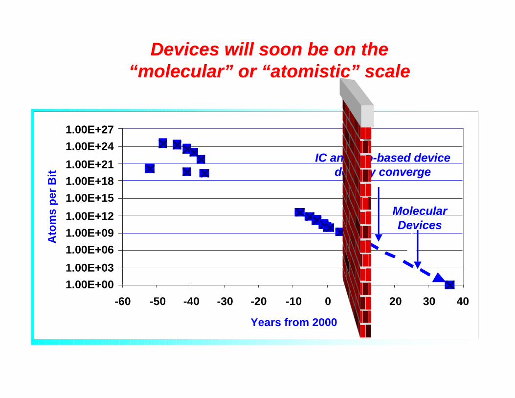
Bit IC and bio-based device
densities converge
Molecular devices
IC and Bio-based deviceIC and Bio-based devicedensity convergedensity converge
MolecularMolecularDevicesDevices
Devices will soon be on theDevices will soon be on the““molecularmolecular”” or or ““atomisticatomistic”” scale scale

6
7
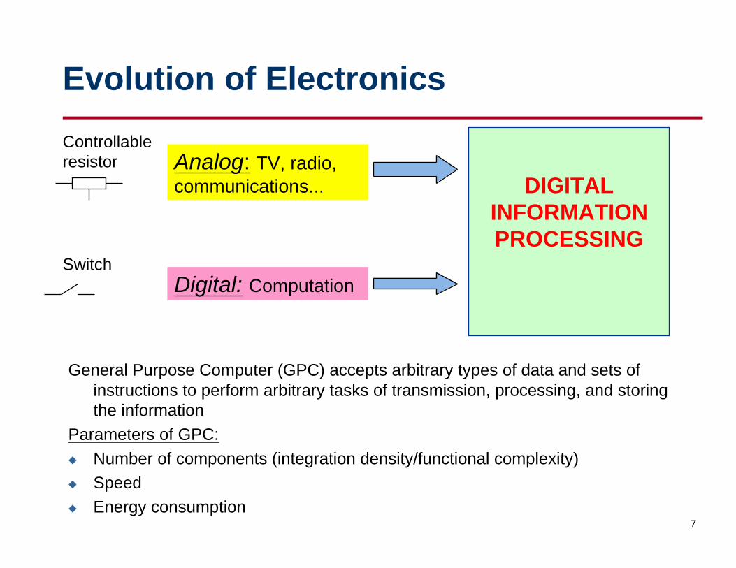
Evolution of Electronics
Analog: TV, radio,communications...
Digital: Computation
DIGITALINFORMATIONPROCESSING
General Purpose Computer (GPC) accepts arbitrary types of data and sets ofinstructions to perform arbitrary tasks of transmission, processing, and storingthe information
Parameters of GPC:
u Number of components (integration density/functional complexity)
u Speed
u Energy consumption
Controllableresistor
Switch
8
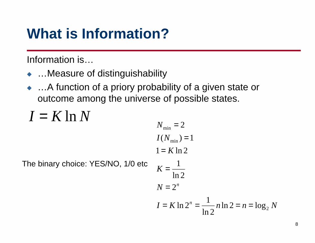
What is Information?
Information is…
u …Measure of distinguishability
u …A function of a priory probability of a given state oroutcome among the universe of possible states.
NKI ln=
NnnKI
N
K
K
NI
N
n
n
2
min
min
log2ln2ln
12ln
2
2ln
1
2ln1
1)(
2
====
=
=
==
=
The binary choice: YES/NO, 1/0 etc

9
Constituents of the Information Theory
u Constituents of the Information Theory• Sender and recipient
• Symbols (microstates) as elementary units of information
u Information carriers
Information is physical!

10
The Abacus, an ancient digitalcalculating device
Information is represented in digital form
Each column denotes a decimal digit
Binary representation: two possible positions for each bead
A bead in the abacus is a memory device, not a logic gate

Source: IBM
12
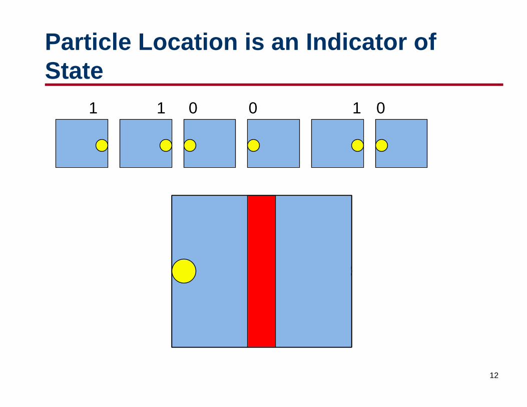
Particle Location is an Indicator ofState
1 1 0 0 1 0

13
Two-well bit
a
a
Eb
Eb
w w

14
A physical system as a computingmediumu We need to create a bit first. Information processing always
requires physical carrier, which are material particles.
u First requirement to physical realization of a bit impliescreating distinguishable states within a system of suchmaterial particles.
u The second requirement is conditional change of state.
u The properties of distinguishability and conditional changeof state are two fundamental properties of a materialsubsystem to represent information. These properties canbe obtained by creating energy barriers in a materialsystem.

15
Kroemer’s Lemma of ProvenIgnorance
u If in discussing a semiconductor problem,you cannot draw an Energy-Band-Diagram,this shows that you don’t know what are youtalking about
u If you can draw one, but don’t, then youraudience won’t know what are you talkingabout

16
Barrier engineering in semiconductors
n n
p
By doping, it is possible to create a built-in field and energy barriers ofcontrollable height and length within semiconductor. It allows one to achieveconditional complex electron transport between different energy states insidesemiconductors that is needed in the physical realization of devices forinformation processing.

17
Heterojunction barriers
a
w
EbDouble barrier
Superlattice

18
Example: Field Effect Transistor
Long Channel Short Channel
It is possible to derive MOSFET I-V equation form thetwo-well one-barrier model

19
Designers and Users want:u Highest possible integration density (n)
v To keep chips size small and increase yieldsv To increase functionality
u Highest possible speed (f=1/t)v Speed sells!
u Lowest possible power consumption (P)v Decrease demands for energyv The generation of too much heat means costly cooling
systems
Ideal von Neumann’s Computer

20
Binary Information Throughput (BIT)
BIT is the maximum number of binarytransition per unit time
fnBIT bit=
1
10
100
1000
10000
2000 2005 2010 2015 2020
Year
BIT
, M
bit
/ns
nbit – the number of binarystates (e.g. transistors)
f-switching frequency
- one measure ofcomputational capability

21
Energetics of Computation
nfEP bit=
Requirements for an ideal computer:
(integration density) n=max
(switching frequency) f=max
(power) P=min
BIT=max
2214®®
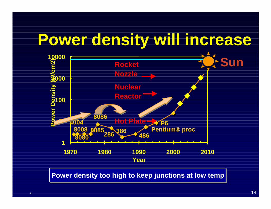
Power density will increase
400480088080
8085
8086
286 386486
Pentium® procP6
1
10
100
1000
10000
1970 1980 1990 2000 2010Year
Po
wer
Den
sity
(W
/cm
2)
Hot Plate
NuclearReactor
RocketNozzle
Power density too high to keep junctions at low tempPower density too high to keep junctions at low temp
Sun

23
Lowest Barrier:Distinguishability Barrier
a
a
Eb
Eb
Distinguishability D implies lowprobability of spontaneous transitionsbetween two wells (error probability)
D=max, =0 D=0, =0.5 (50%)
Classic distinguishability:)exp(
Tk
E
B
bclassic −=Π
Minimum distinguishable barrier: _=0.5
)exp(2
1
Tk
E
B
b−= Eb=kTln2Shannon - von Neumann - Landauer limit

24
Smallest Size:The Heisenberg Barrier
hh
≥∆∆≥∆∆
tE
px
b
b
crit
Et
mEa
h
h
=
=
min
2
Eb=kTln2

25
Classic and QuantumDistinguishability @ =0.5
2ln
)exp(
min TkE
Tk
E
Bb
B
bclassic
=
−=Π
2
22min
8
2ln
)22
exp(
maE
Eam
b
bquantum
hh
=
−=Π
aEb
aEb
aEb
aEb
WKB: (Tunneling)
26
Total Distinguishability @ =0.5
Generalized expression forthe minimum energy barrierto create a bit
2
22min
8
)2(ln2ln
makTEb
h+≈
)22
exp()22
exp()exp(kT
mEakTEEa
m
kT
E bbb
b
quantumclassicquantumclassicerror
hh
h+
−−−+−=
=ΠΠ−Π+Π=Π
0.6
0.7
0.8
0.9
1
1.1
1.2
0 5 10 15 20
a, nmE b
/kT
kTln2
27
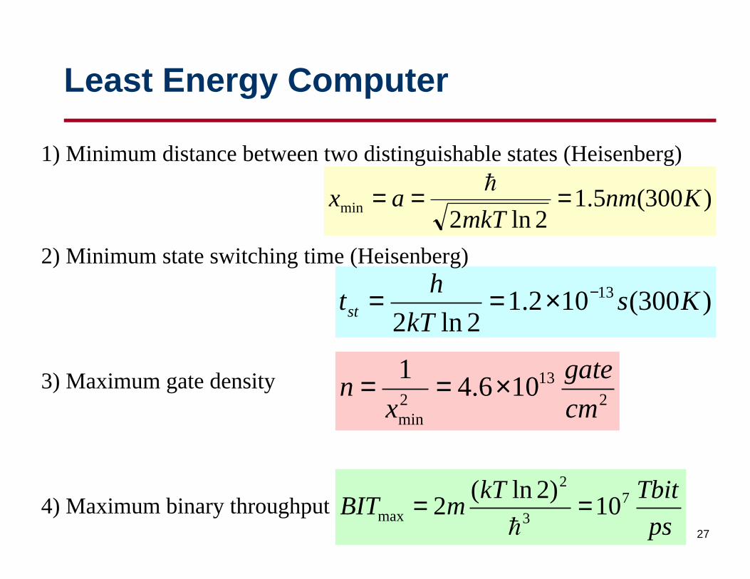
Least Energy Computer
)300(5.12ln2
min KnmmkT
ax === h
)300(102.12ln2
13 KskT
htst
−×==
213
2min
106.41
cm
gate
xn ×==
1) Minimum distance between two distinguishable states (Heisenberg)
2) Minimum state switching time (Heisenberg)
3) Maximum gate density
4) Maximum binary throughputps
TbitkTmBIT 7
3
2
max 10)2ln(
2 ==h

28
Total Power Consumption atMinimal Energy per bit - {kTln(2)}
2)2ln(22ln
kTht
kT
t
EP
scsc
bbit === bitchip nPP =
261074.4
cm
WPchip ×= T=300 K
The circuit would vaporize when it is turned on!

29
Single Electron Devices Don’t Avoid the PowerProblem
w
eEa
04=
2w
fEfnEP a
a ==f=10 GHz
00.05
0.1
0.150.2
0.250.3
0.350.4
0 5 10 15 20
w, nm
Ea
, e
V
1
10
100
1000
10000
100000
0 10 20 30
w, nmP
ow
er,
W/c
m2
w
Electrostatic energyto add an electron toa particle with size w
e- Ebit>Ea
In sub-10 nm single electron devices, the minimum energy toadd/remove electron is much larger than kT, and it increases assize deceases.

30
Power vs. Error trade-off
0.E+00
2.E+07
4.E+07
6.E+07
8.E+07
1.E+08
1.E+08
0 0.1 0.2 0.3 0.4 0.5 0.6
err
Pto
tal, W
Πerr
False bitoccurrence
Additional Static(leakage) power
Computation at Πerr=0.5 is impossible
In useful computation, Πerr <<0.5,hence much larger total power isneeded
a=1nm;n=1014 bit/cm2;f=3x1013 Hz

31
Dynamic and Static Power
)()( berrdb
berroffs
bb
ond
EP
e
EEefnViP
fnEe
EefnVIP
Π=⋅Π⋅⋅==
=⋅⋅⋅==
1.00E+04
1.00E+05
1.00E+06
1.00E+07
1.00E+08
1.00E+09
0 0.05 0.1 0.15 0.2 0.25
Eb, eV
P,
W
dynamic powerstatic powertotal power
a=1nm; n=1014 bit/cm2; f=3x10¹³ Hz
α=1 α=0.05
1.00E+04
1.00E+05
1.00E+06
1.00E+07
1.00E+08
1.00E+09
0 0.05 0.1 0.15 0.2 0.25
Eb, eV
P,
W
dynamic powerstatic powertotal power
kT

32
Will Spintronics Alleviate the PowerProblem?
u Expectations:v ultra low power ???v ultra high density ???
u A quote: “Spintronics would use much less power than conventional electronics,because the energy needed to change a spin is a minute fraction of what isneeded to push charge around”
u Is the very low energy to change state an advantage (e.g. low dynamicpower) or a disadvantage (e.g. high error probability) for applications ofspin devices in information processing?
0 1 E↑
E↓
Br
BE B2=∆
∆E=2 µB B = 2_9.27_10-24 J / T_1.5 T =2.78_10-23 J= 1.74_10-4 eV
99.02
exp =
−=Π
kT
BBerr
Example:
T=300 K
B=1.5 T(practically viable) (µB = 9.27_10-24 J / T)

33
How much heat a solid systemcan tolerate?…
ITRS 2001 projects 93 W/cm2 for MPU in 2016
Several hundred W/cm2 is close to known limits ofheat removal from a 2-dimensional solid materialstructure with Tmax =125°C
Experimental demonstrations of on-Si cooling systems(without active devices):
680 W/cm2 thermoelectric (Zheng et al.)
790 W/cm2 microchannel (Tuckerman and Pease)
34
…and implications to the Roadmap:Inflexion of ITRS vectors?
l is the “cell size”:
I=n-1/2
lmin=a
lMPU=(11-15)a
300 K
1.00E-13
1.00E-12
1.00E-11
1.00E-10
1.00E-09
1.00E-08
1 10 100 1000
l, nm
t, s
Memory
Logic
l
Heisenberg barrier
Heisenberg barrier
P=100 W/cm2
1
2
4
3

35
Implications for NanoelectronicsUtilizing ElectronTransport
u Scaling to molecular dimensions may not yieldperformance increasesv We will be forced to trade-off between speed and density
u Optimal dimensions (depending on speed/density trade-offs) for electronic switches should range between 5 and50 nm, and this may be achievable with silicon technologyv Within the scope of ITRS projections

36
Fundamentals of Heat Removal
Quotes from anonymous scientists working at the frontiers ofnanoelectronics:
“ Heat removal is not an issue. Simply, engineers must inventbetter technologies for heat removal and cooling ”.
“Heat can be dissipated somewhere else”
Three fundamentals of heat removal:
1)The Newton's Law of Cooling: q=h(Th-Ta)(h-heat transfer coefficient)
2) The Ambient: Ta=300 K !!!
3) The Carnot’s theorem:
−−= QT
TTW
c
cacool
Heat to beremoved
Work tobe done

37
Newton’s law of cooling
Cooling method h, W/cm2·K . Air, natural convection 0.001 Air, forced convection 0.01 . Water, natural convection 0.1 Water, forced convection 1
. Boiling 10
Q=h*A**(Th-Ta) max (Th-Ta)=100K
Max P=1000 W/cm2 ? (A=const)*h – the heat transfer coefficient**A - area

38
The ambient interface
R1
Q1 Refrigerator
Chip interface Ambient interface
AirChip
Q2=Q1+W
R2
W
Tj AhR
1=
air, T=300 K
Ahot<<Acold
Device
Lbox
Boiling
A1
A2
- thermalresistance
12
12
hh
<>
A2>A1
Surface extension isessential for removal ofhigh heat fluxes to theenvironment
39
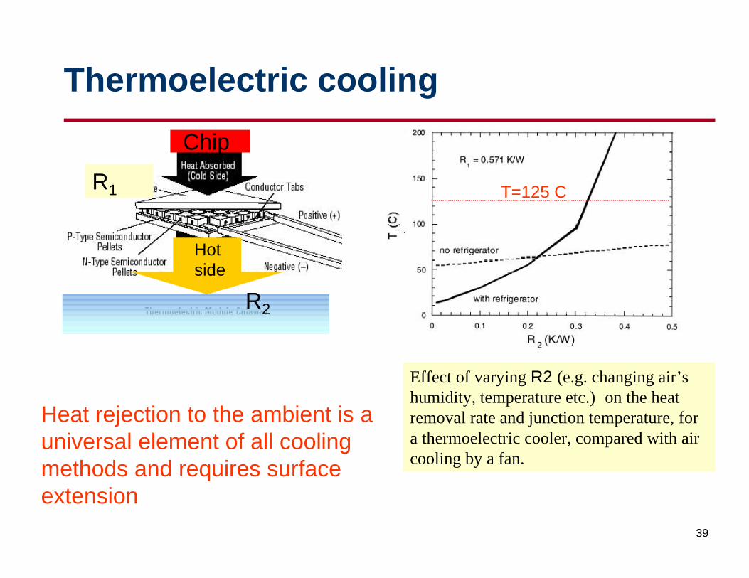
Thermoelectric cooling
T=125 C
Effect of varying R2 (e.g. changing air’shumidity, temperature etc.) on the heatremoval rate and junction temperature, fora thermoelectric cooler, compared with aircooling by a fan.
R1
R2
Hotside
Heat rejection to the ambient is auniversal element of all coolingmethods and requires surfaceextension
Chip

40
How Much Volume is Needed to TransferChip Heat to the Ambient?
Example:n=1014 bit/cm2
t=0.01 ps
BIT=104 Tbit/ps
a=1 nm
Ebit=0.08 eV (~4kT)
Πerror=10% /device
P=107 W/cm2
Th
PA
nccold ∆
>
Box size:
Acold>2x108 cm2
Lbox>141 m
Air: Ta=300 K
h=0.001 W/cm2KCold wall:
Q>107 W
Tcold=350 K
Thot=400 K
P=107 W;Ahot=1 cm2
Lbox
Q>P
Very Big Box!
P, W Approx. box dimensions, cm 1 3x3x0.5
10 10x8x1100 30x20x8
1000 100x50x4010000 182x182x182
Example: computer min. size vs power

41
Carnot’s Refrigerator andCryogenic Computation
−−= QT
TTW
c
cacool
Min. total power needed to run a 100 W chip:
at 77 K - 300 W
at 4.2 K - 7 kW
The efficiency of heat engines dramatically drops at T<<Ta

42
Cryogenic Computation with nanodevices
2ln8
)2(ln2ln
8
)2(ln2ln
2
22
2
22
aBdev
aaB
devBdev
abit
dev
abit
dev
devabit
totalbit
TkmaT
TTk
maTk
T
TE
T
TE
T
TTEE
>+=
=
+==−+=
h
h
10.00
100.00
1000.00
0 5 10 15 20
a, nm
E b,
me
V (
tota
l)
T=300K
T=4KDue to tunneling, thepower consumed by thedevice depends on bothoperating temperature andsize that manifests itselfwith unexpectedly dramaticincreases in total powerconsumption at cryogenictemperatures.

43
The barriers dilemma
u Energy barriers are key components to provide InformationFlow
u Energy barriers are negative factor for Heat Flow
u Can we think of radically new ways of heat removal basedon coherent heat flows, e.g. heat lasers or solitons?
ReflectionTransmission
A driver for physical layout?
phonons

44
A question – What to do?
Substrate
Gate
Source Drain
IBM CNTFET
Silicon MOSFET
?

45
Energy efficiency of CMOS
Does practical CMOS operate far from fundamental limits?
u 2016 ITRS 22-nm Node:
v xmin: Channel length 9 nm
v Esw: Switching energy 2 x 10-18 J
v Eb: S-Ch barrier height ~0.4 eV
v Electrons/switching event ~50
v Energy/electron 4 x 10-20 J~12 kT
)300(5.12ln2
min KnmmkT
ax === h
Eb>kTln2=0.02 eV
Esw > kTln2 = 3 x 10-21 J
1
3 x 10-21J ~ kT
Fundamental limits

46
Can we decrease the energy ofCMOS?
2 x 10-18 J 3 x 10-21J
Decrease the barrier height:
0.4 eV 0.02 eV
Yes (in principle):
Decrease the number ofelectron per switching event:
50 1)exp(
kT
Eberr −=ΠEb
12kT 0.001%
0.03%8kT
2%4kT
50%kT ln2

47
What to do? (Cont’d)
Quantum Computer
Cellular Non Linear Network
Conventional von NeumannArchitecture
New InformationProcessing Architectures
?
Substrate
Gate
Source Drain
Silicon MOSFET

48
2003 ITRS: Emerging ResearchDevices
Device
FET
RSFQ 1D
struct RTD SET
Molecular
QCA Spin
transistor Density (dev/cm2)
3E9 106 3E9 3E9 6E10 1012 3E10 3E9
Switch Speed
700 GHz
1.2 THz ? 1 THz 1GHz ? 30 MHz 700 GHz
Circuit Speed
30 GHz
400 GHz 30 GHz 30 GHz 100 MHz 1 MHz 1 MHz 30 GHz
Switching energy, J
2E-18 2x 10-19
[>1.4E-17 2E-18 >2E-18
10-18 [>1.5E-17]
1.3x10⁻¹⁶ E: [> 10-18 ] M:>4x10-17
2 x 10-18
Binary throughput, GBit/ns/cm2
86 0.4 86 86 10 ? 0.06 86

49
Classic to Quantum transition
u Classic memory bits become indistinguishable, which limitsour ability to use them for computation
BUT
u The superposition of indistinguishable states is a keyconcept of Quantum Computation
u A quantum bit or qbit is a physical system with twoquantum states

50
Power of quantum computing
u Quantum information storagev N quantum bits stores 2N complex numbers
n Consider information in 300 entangled qubits
2300 = 1090
n Compare to the total number of atoms in the Universe:
Natoms=1080
If dramatic improvement of the information throughput can be achieved, the cryogenic operation might be affordable
51
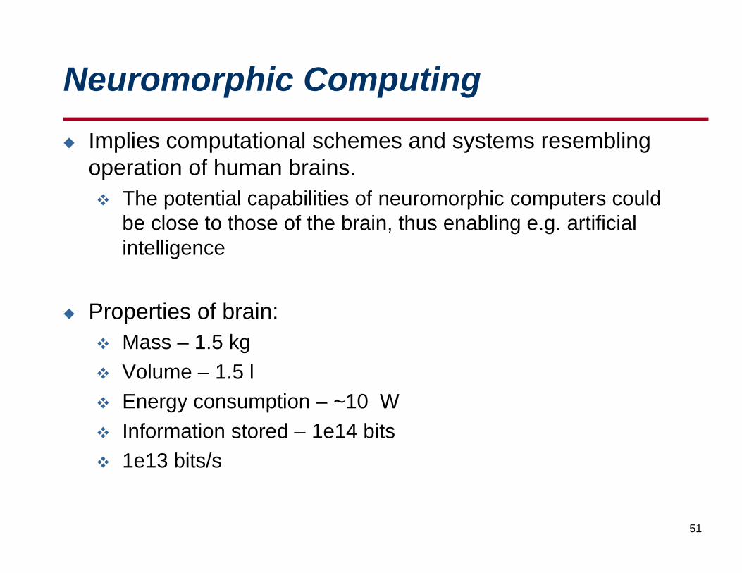
Neuromorphic Computing
u Implies computational schemes and systems resemblingoperation of human brains.v The potential capabilities of neuromorphic computers could
be close to those of the brain, thus enabling e.g. artificialintelligence
u Properties of brain:v Mass – 1.5 kg
v Volume – 1.5 l
v Energy consumption – ~10 W
v Information stored – 1e14 bits
v 1e13 bits/s

52
Conclusions
v Fundamental considerations suggest that the potentialbenefits from replacing CMOS devices with new types ofelectron transport devices may be limited
v Search for radically new methods of heat removal is one ofthe most critical research directions
v The exploration of alternative approaches to von Neumanntype computing, such as brain or Reversible/QuantumComputation, is becoming a strategic imperative.
n We need a concerted effort in these areas because of the longlead times for the introduction of radically new technologies