Embed Size (px)
Citation preview

R
Virtex-5 FPGA XtremeDSP Design ConsiderationsUser Guide
UG193 (v3.6) July 27, 2017
Virtex-5 FPGA XtremeDSP Design Considerations www.xilinx.com UG193 (v3.6) July 27, 2017
The information disclosed to you hereunder (the “Materials”) is provided solely for the selection and use of Xilinx products. To the maximumextent permitted by applicable law: (1) Materials are made available "AS IS" and with all faults, Xilinx hereby DISCLAIMS ALLWARRANTIES AND CONDITIONS, EXPRESS, IMPLIED, OR STATUTORY, INCLUDING BUT NOT LIMITED TO WARRANTIES OFMERCHANTABILITY, NON-INFRINGEMENT, OR FITNESS FOR ANY PARTICULAR PURPOSE; and (2) Xilinx shall not be liable (whetherin contract or tort, including negligence, or under any other theory of liability) for any loss or damage of any kind or nature related to, arisingunder, or in connection with, the Materials (including your use of the Materials), including for any direct, indirect, special, incidental, orconsequential loss or damage (including loss of data, profits, goodwill, or any type of loss or damage suffered as a result of any actionbrought by a third party) even if such damage or loss was reasonably foreseeable or Xilinx had been advised of the possibility of the same.Xilinx assumes no obligation to correct any errors contained in the Materials or to notify you of updates to the Materials or to productspecifications. You may not reproduce, modify, distribute, or publicly display the Materials without prior written consent. Certain products aresubject to the terms and conditions of Xilinx’s limited warranty, please refer to Xilinx’s Terms of Sale which can be viewed athttps://www.xilinx.com/legal.htm#tos; IP cores may be subject to warranty and support terms contained in a license issued to you by Xilinx.Xilinx products are not designed or intended to be fail-safe or for use in any application requiring fail-safe performance; you assume sole riskand liability for use of Xilinx products in such critical applications, please refer to Xilinx’s Terms of Sale which can be viewed athttps://www.xilinx.com/legal.htm#tos.
© Copyright 2006–2017 Xilinx, Inc. XILINX, the Xilinx logo, Virtex, Spartan, ISE, and other designated brands included herein are trademarks of Xilinx in the United States and other countries. PowerPC is a trademark of IBM Corp. and is used under license. All other trademarks are the property of their respective owners.
Revision HistoryThe following table shows the revision history for this document.
R
Date Version Revision
04/14/06 1.0 Initial Xilinx release.
05/12/06 1.1 Typographical edits.
06/06/06 1.2 Updated “PATTERNDETECT and PATTERNBDETECT Port Logic,”“Overflow and Underflow Port Logic,” “Adder Tree,”and “DSP48E Instantiation Templates.” Updated Table 1-3, Table 3-1, Figure 1-19, Figure 4-22, Figure 4-23, Figure 4-35, and Figure 4-40. Added “Reference Design Files”section and link to design files.
07/28/06 1.3 Updated Table 1-2, Table 1-3, Table 1-5, Table 1-10, Figure 1-6, Figure 1-16, Figure 1-17, Figure 1-18, Figure 2-3, Figure 2-4, Figure 4-4, Figure 4-8, Figure 4-21, Figure 4-25, Figure 4-26, Figure 4-28, Figure 4-38, Figure 4-39, the “Two Input Logic Unit” section and renamed and reorganized the “Filters” section. Updated Equation 4-9. Removed Table 4-1. Also made typographical edits.
09/06/06 2.0 Updated Table 1-1. Also made minor typographical edits.
10/12/06 2.1 Updated Chapter 1: “Overflow and Underflow Logic,” “Architectural Highlights,” Table 1-10, and “Pattern Detect Logic.”Updated Chapter 4: “Extended Multiply,” “Two Input 48-Bit Dynamic Add/Subtract,” “MACC and MACC Extension,” “Overflow/Underflow/Saturation Past P[46],” Equation 4-3, Table 4-2, Figure 4-1, Figure 4-10, Figure 4-14, Figure 4-22, Figure 4-23, Figure 4-25, Figure 4-34, Figure 4-35, Figure 4-36, and Figure 4-37. Also, other typographical edits.
02/02/07 2.2 Updated Table 1-1, page 18 with Virtex-5 LX220T and SXT device information. Also updated “Multiplexer Selection,” page 57.

UG193 (v3.6) July 27, 2017 www.xilinx.com Virtex-5 FPGA XtremeDSP Design Considerations
03/20/07 2.3 Updated “Dynamic Shifter” and “18-Bit Barrel Shifter” sections and Figure 4-2, Figure 4-3. Added “Floating Point Multiply and 59 x 59 Signed Multiply” and Figure 4-15 and Figure 4-16.
05/17/07 2.4 Updated the “X, Y, and Z Multiplexer” section.
05/22/07 2.4.1 Typographical edits.
08/01/07 2.5 Updated Figure 2-2, Figure 4-21, and Figure 4-22.
10/09/07 2.6 Updated disclaimer.
Chapter 1: Updated Equation 1-1 and “ALUMODE Inputs” and “MULTSIGNOUT Port Logic”sections.
Chapter 4: Updated the “Convergent Rounding: LSB Correction Technique” section.
Added Appendix A.
Made minor typographical edits.
12/11/07 2.7 Updated Table 1-1 with Virtex-5 LX155, LX20T, and LX155T devices. Updated Figure 1-12.
02/05/08 2.8 Made minor typographical edits.
Chapter 2: Updated the “Designing for Performance (to 550 MHz)” and “Adder/Subtracter or Logic Unit” sections.
03/31/08 3.0 Made minor typographical edits.
Updated “About This Guide.”
Chapter 1: Updated Figure 1-3 and Table 1-1 (added FXT devices).
Chapter 4: Updated Figure 4-16.
04/25/08 3.1 Updated Table 1-1 with SX240T device.
09/23/08 3.2 Added the TXT platform.
Chapter 1: Updated Table 1-1.
01/12/09 3.3 Chapter 2: Updated Figure 2-2.
Chapter 4: Updated “MACC and MACC Extension” section, Figure 4-23, Figure 4-27, and Figure 4-37.
Appendix A: Updated “MULTSIGNOUT and CARRYCASCOUT” section.
06/01/10 3.4 Chapter 1: Added encoding to the MASK description in Table 1-3.
Chapter 2: Removed the “Connecting DSP48E Slices and Block RAM“ section. Changed the input labels in Figure 2-3 and Figure 2-4 to match Equation 2-1 through Equation 2-3.
Chapter 4: Updated the MACC and MACC Extension section. Replaced Figure 4-23. Changed both output buses in Figure 4-24 from [42:0] to [43:0]. Changed the input bus to the top slice in Figure 4-27 from a[17:0] to b[17:0].
Chapter 5: Updated hyperlinks.
01/26/12 3.5 Updated “Convergent Rounding” and “Convergent Rounding: LSB Correction Technique.” Updated titles of Table 4-6 and Table 4-7.
Date Version Revision

Virtex-5 FPGA XtremeDSP Design Considerations www.xilinx.com UG193 (v3.6) July 27, 2017
07/27/17 3.6 Updated links to Xilinx documentation in “About This Guide.”
Chapter 4: Reversed order of DSP48E headings in Table 4-1.
Chapter 5: Updated “Synthesis Tools.” Added link to DSP IP Core web page in “DSP IP.” Updated link to System Generator for DSP User Guide in “System Generator for DSP.” Removed link to ISE software manuals in “Architecture Wizard.”
Date Version Revision

Virtex-5 FPGA XtremeDSP Design Considerations www.xilinx.com 5UG193 (v3.6) July 27, 2017
Revision History . . . . . . . . . . . . . . . . . . . . . . . . . . . . . . . . . . . . . . . . . . . . . . . . . . . . . . . . . . . . . 2
Preface: About This GuideGuide Contents . . . . . . . . . . . . . . . . . . . . . . . . . . . . . . . . . . . . . . . . . . . . . . . . . . . . . . . . . . . . . . 9Additional Documentation . . . . . . . . . . . . . . . . . . . . . . . . . . . . . . . . . . . . . . . . . . . . . . . . . . . 9Additional Support Resources . . . . . . . . . . . . . . . . . . . . . . . . . . . . . . . . . . . . . . . . . . . . . . . 10Typographical Conventions . . . . . . . . . . . . . . . . . . . . . . . . . . . . . . . . . . . . . . . . . . . . . . . . . 11
Online Document . . . . . . . . . . . . . . . . . . . . . . . . . . . . . . . . . . . . . . . . . . . . . . . . . . . . . . . . . 11
Chapter 1: DSP48E Description and SpecificsIntroduction . . . . . . . . . . . . . . . . . . . . . . . . . . . . . . . . . . . . . . . . . . . . . . . . . . . . . . . . . . . . . . . . 13Architectural Highlights . . . . . . . . . . . . . . . . . . . . . . . . . . . . . . . . . . . . . . . . . . . . . . . . . . . . 14
DSP48E Tile and Interconnect . . . . . . . . . . . . . . . . . . . . . . . . . . . . . . . . . . . . . . . . . . . . . . 17Number of DSP48E Slices per Virtex-5 Device . . . . . . . . . . . . . . . . . . . . . . . . . . . . . . . . 18DSP48E Slice Primitive . . . . . . . . . . . . . . . . . . . . . . . . . . . . . . . . . . . . . . . . . . . . . . . . . . . . 18
Simplified DSP48E Slice Operation . . . . . . . . . . . . . . . . . . . . . . . . . . . . . . . . . . . . . . . . . 21DSP48E Slice Attributes . . . . . . . . . . . . . . . . . . . . . . . . . . . . . . . . . . . . . . . . . . . . . . . . . . . 23Input Ports . . . . . . . . . . . . . . . . . . . . . . . . . . . . . . . . . . . . . . . . . . . . . . . . . . . . . . . . . . . . . . . 27
A, B, and C Ports. . . . . . . . . . . . . . . . . . . . . . . . . . . . . . . . . . . . . . . . . . . . . . . . . . . . . . . 28OPMODE, ALUMODE, and CARRYINSEL Port Logic . . . . . . . . . . . . . . . . . . . . . . . . . 30X, Y, and Z Multiplexer. . . . . . . . . . . . . . . . . . . . . . . . . . . . . . . . . . . . . . . . . . . . . . . . . . 31ALUMODE Inputs . . . . . . . . . . . . . . . . . . . . . . . . . . . . . . . . . . . . . . . . . . . . . . . . . . . . . 32Carry Input Logic . . . . . . . . . . . . . . . . . . . . . . . . . . . . . . . . . . . . . . . . . . . . . . . . . . . . . . 33
Output Ports . . . . . . . . . . . . . . . . . . . . . . . . . . . . . . . . . . . . . . . . . . . . . . . . . . . . . . . . . . . . . 34P Port . . . . . . . . . . . . . . . . . . . . . . . . . . . . . . . . . . . . . . . . . . . . . . . . . . . . . . . . . . . . . . . 35CARRYCASCOUT and CARRYOUT Ports . . . . . . . . . . . . . . . . . . . . . . . . . . . . . . . . . . 36MULTSIGNOUT Port Logic . . . . . . . . . . . . . . . . . . . . . . . . . . . . . . . . . . . . . . . . . . . . . . 36PATTERNDETECT and PATTERNBDETECT Port Logic . . . . . . . . . . . . . . . . . . . . . . . 37Overflow and Underflow Port Logic . . . . . . . . . . . . . . . . . . . . . . . . . . . . . . . . . . . . . . . 37
Embedded Functions . . . . . . . . . . . . . . . . . . . . . . . . . . . . . . . . . . . . . . . . . . . . . . . . . . . . . . 37Two’s Complement Multiplier . . . . . . . . . . . . . . . . . . . . . . . . . . . . . . . . . . . . . . . . . . . . 38Adder/Subtracter or Logic Unit . . . . . . . . . . . . . . . . . . . . . . . . . . . . . . . . . . . . . . . . . . . 39Two Input Logic Unit . . . . . . . . . . . . . . . . . . . . . . . . . . . . . . . . . . . . . . . . . . . . . . . . . . . 39
Single Instruction, Multiple Data (SIMD) Mode . . . . . . . . . . . . . . . . . . . . . . . . . . . . . . . 40Pattern Detect Logic . . . . . . . . . . . . . . . . . . . . . . . . . . . . . . . . . . . . . . . . . . . . . . . . . . . . . . . 41
Overflow and Underflow Logic . . . . . . . . . . . . . . . . . . . . . . . . . . . . . . . . . . . . . . . . . . . 42Auto Reset Logic. . . . . . . . . . . . . . . . . . . . . . . . . . . . . . . . . . . . . . . . . . . . . . . . . . . . . . . 44
Chapter 2: DSP48E Design ConsiderationsIntroduction . . . . . . . . . . . . . . . . . . . . . . . . . . . . . . . . . . . . . . . . . . . . . . . . . . . . . . . . . . . . . . . . 45Designing for Performance (to 550 MHz) . . . . . . . . . . . . . . . . . . . . . . . . . . . . . . . . . . . . 45Designing for Power . . . . . . . . . . . . . . . . . . . . . . . . . . . . . . . . . . . . . . . . . . . . . . . . . . . . . . . . 45Adder Tree vs. Adder Chain . . . . . . . . . . . . . . . . . . . . . . . . . . . . . . . . . . . . . . . . . . . . . . . . . 45
Adder Tree . . . . . . . . . . . . . . . . . . . . . . . . . . . . . . . . . . . . . . . . . . . . . . . . . . . . . . . . . . . . . . 45
Table of Contents

6 www.xilinx.com Virtex-5 FPGA XtremeDSP Design ConsiderationsUG193 (v3.6) July 27, 2017
R
Adder Cascade . . . . . . . . . . . . . . . . . . . . . . . . . . . . . . . . . . . . . . . . . . . . . . . . . . . . . . . . . . . 48Connecting DSP48E Slices across Columns . . . . . . . . . . . . . . . . . . . . . . . . . . . . . . . . . . 50Time Multiplexing the DSP48E Slice . . . . . . . . . . . . . . . . . . . . . . . . . . . . . . . . . . . . . . . . 50Miscellaneous Notes and Suggestions . . . . . . . . . . . . . . . . . . . . . . . . . . . . . . . . . . . . . . . 50
Chapter 3: DSP48E Timing ConsiderationDSP48E Switching Characteristics . . . . . . . . . . . . . . . . . . . . . . . . . . . . . . . . . . . . . . . . . . . 53Timing Diagram . . . . . . . . . . . . . . . . . . . . . . . . . . . . . . . . . . . . . . . . . . . . . . . . . . . . . . . . . . . . 56
Chapter 4: DSP48E ApplicationsIntroduction . . . . . . . . . . . . . . . . . . . . . . . . . . . . . . . . . . . . . . . . . . . . . . . . . . . . . . . . . . . . . . . . 57Multiplexer Selection . . . . . . . . . . . . . . . . . . . . . . . . . . . . . . . . . . . . . . . . . . . . . . . . . . . . . . . 57HDL Instantiation. . . . . . . . . . . . . . . . . . . . . . . . . . . . . . . . . . . . . . . . . . . . . . . . . . . . . . . . . . . 57Application Examples . . . . . . . . . . . . . . . . . . . . . . . . . . . . . . . . . . . . . . . . . . . . . . . . . . . . . . . 58
Logic and Bit Field Application . . . . . . . . . . . . . . . . . . . . . . . . . . . . . . . . . . . . . . . . . . . . . 58Two 48-Bit Input Bitwise Logic Functions . . . . . . . . . . . . . . . . . . . . . . . . . . . . . . . . . . . 58Dynamic Shifter . . . . . . . . . . . . . . . . . . . . . . . . . . . . . . . . . . . . . . . . . . . . . . . . . . . . . . . 5818-Bit Barrel Shifter . . . . . . . . . . . . . . . . . . . . . . . . . . . . . . . . . . . . . . . . . . . . . . . . . . . . . 6048-Bit Counter. . . . . . . . . . . . . . . . . . . . . . . . . . . . . . . . . . . . . . . . . . . . . . . . . . . . . . . . . 62Single Instruction Multiple Data (SIMD) Arithmetic . . . . . . . . . . . . . . . . . . . . . . . . . . . 62SIMD Absolute Value (24) . . . . . . . . . . . . . . . . . . . . . . . . . . . . . . . . . . . . . . . . . . . . . . . 63Bus Multiplexer. . . . . . . . . . . . . . . . . . . . . . . . . . . . . . . . . . . . . . . . . . . . . . . . . . . . . . . . 64
Basic Math Applications . . . . . . . . . . . . . . . . . . . . . . . . . . . . . . . . . . . . . . . . . . . . . . . . . . . 6525 x 18 Two's Complement Multiply . . . . . . . . . . . . . . . . . . . . . . . . . . . . . . . . . . . . . . . 65Two Input 48-Bit Addition . . . . . . . . . . . . . . . . . . . . . . . . . . . . . . . . . . . . . . . . . . . . . . . 66Four Input 46-Bit Addition . . . . . . . . . . . . . . . . . . . . . . . . . . . . . . . . . . . . . . . . . . . . . . . 66Two Input 48-Bit Dynamic Add/Subtract . . . . . . . . . . . . . . . . . . . . . . . . . . . . . . . . . . . 67Three Input 47-Bit Dynamic Add/Subtract . . . . . . . . . . . . . . . . . . . . . . . . . . . . . . . . . . 6825 x 18 Multiply Plus 48-Bit Add/Sub . . . . . . . . . . . . . . . . . . . . . . . . . . . . . . . . . . . . . . 69Extended Multiply . . . . . . . . . . . . . . . . . . . . . . . . . . . . . . . . . . . . . . . . . . . . . . . . . . . . . 70Floating Point Multiply and 59 x 59 Signed Multiply . . . . . . . . . . . . . . . . . . . . . . . . . . . 7125 x 18 Multiply Plus 48-Bit Add Cascade . . . . . . . . . . . . . . . . . . . . . . . . . . . . . . . . . . . 74Division. . . . . . . . . . . . . . . . . . . . . . . . . . . . . . . . . . . . . . . . . . . . . . . . . . . . . . . . . . . . . . 74
Advanced Math Applications . . . . . . . . . . . . . . . . . . . . . . . . . . . . . . . . . . . . . . . . . . . . . . 75Accumulate. . . . . . . . . . . . . . . . . . . . . . . . . . . . . . . . . . . . . . . . . . . . . . . . . . . . . . . . . . . 75Two Input 48-Bit Add Accumulate. . . . . . . . . . . . . . . . . . . . . . . . . . . . . . . . . . . . . . . . . 75Dynamic Add/Sub Accumulate . . . . . . . . . . . . . . . . . . . . . . . . . . . . . . . . . . . . . . . . . . . 7696-Bit Add/Subtract . . . . . . . . . . . . . . . . . . . . . . . . . . . . . . . . . . . . . . . . . . . . . . . . . . . . 7796-Bit Accumulator . . . . . . . . . . . . . . . . . . . . . . . . . . . . . . . . . . . . . . . . . . . . . . . . . . . . . 77MACC and MACC Extension . . . . . . . . . . . . . . . . . . . . . . . . . . . . . . . . . . . . . . . . . . . . . 7825 x 18 Complex Multiply. . . . . . . . . . . . . . . . . . . . . . . . . . . . . . . . . . . . . . . . . . . . . . . . 8035 x 25 Complex Multiply. . . . . . . . . . . . . . . . . . . . . . . . . . . . . . . . . . . . . . . . . . . . . . . . 8125 x 18 Complex MACC . . . . . . . . . . . . . . . . . . . . . . . . . . . . . . . . . . . . . . . . . . . . . . . . . 83
Filters . . . . . . . . . . . . . . . . . . . . . . . . . . . . . . . . . . . . . . . . . . . . . . . . . . . . . . . . . . . . . . . . . . . 87Polyphase Interpolating FIR Filter . . . . . . . . . . . . . . . . . . . . . . . . . . . . . . . . . . . . . . . . . 87Polyphase Decimating FIR Filter . . . . . . . . . . . . . . . . . . . . . . . . . . . . . . . . . . . . . . . . . . 88Multichannel FIR . . . . . . . . . . . . . . . . . . . . . . . . . . . . . . . . . . . . . . . . . . . . . . . . . . . . . . 90Preloading Filter Coefficients . . . . . . . . . . . . . . . . . . . . . . . . . . . . . . . . . . . . . . . . . . . . . 91
Pattern Detect Applications . . . . . . . . . . . . . . . . . . . . . . . . . . . . . . . . . . . . . . . . . . . . . . . . 93Dynamic C Input Pattern Match . . . . . . . . . . . . . . . . . . . . . . . . . . . . . . . . . . . . . . . . . . . 94

Virtex-5 FPGA XtremeDSP Design Considerations www.xilinx.com 7UG193 (v3.6) July 27, 2017
R
Overflow/Underflow/Saturation Past P[46] . . . . . . . . . . . . . . . . . . . . . . . . . . . . . . . . . 94Overflow/Underflow/Saturation Past P[47] . . . . . . . . . . . . . . . . . . . . . . . . . . . . . . . . . 95Logic Unit and Pattern Detect. . . . . . . . . . . . . . . . . . . . . . . . . . . . . . . . . . . . . . . . . . . . . 9548-Bit Counter Auto Reset . . . . . . . . . . . . . . . . . . . . . . . . . . . . . . . . . . . . . . . . . . . . . . . 97
Rounding Applications . . . . . . . . . . . . . . . . . . . . . . . . . . . . . . . . . . . . . . . . . . . . . . . . . . . . 98Rounding Decisions . . . . . . . . . . . . . . . . . . . . . . . . . . . . . . . . . . . . . . . . . . . . . . . . . . . . 98Dynamic or Static Decimal Point . . . . . . . . . . . . . . . . . . . . . . . . . . . . . . . . . . . . . . . . . . 98Symmetric Rounding . . . . . . . . . . . . . . . . . . . . . . . . . . . . . . . . . . . . . . . . . . . . . . . . . . . 98Random Round. . . . . . . . . . . . . . . . . . . . . . . . . . . . . . . . . . . . . . . . . . . . . . . . . . . . . . . . 99Convergent Rounding . . . . . . . . . . . . . . . . . . . . . . . . . . . . . . . . . . . . . . . . . . . . . . . . . . 99Convergent Rounding: LSB Correction Technique . . . . . . . . . . . . . . . . . . . . . . . . . . . . 101Dynamic Convergent Rounding: Carry Correction Technique. . . . . . . . . . . . . . . . . . . 103
Reference Design Files . . . . . . . . . . . . . . . . . . . . . . . . . . . . . . . . . . . . . . . . . . . . . . . . . . . . . 105
Chapter 5: DSP48E Software and Tool Support OverviewIntroduction . . . . . . . . . . . . . . . . . . . . . . . . . . . . . . . . . . . . . . . . . . . . . . . . . . . . . . . . . . . . . . . 107DSP48E Instantiation Templates . . . . . . . . . . . . . . . . . . . . . . . . . . . . . . . . . . . . . . . . . . . 107DSP48E Software Tools . . . . . . . . . . . . . . . . . . . . . . . . . . . . . . . . . . . . . . . . . . . . . . . . . . . . 107
Synthesis Tools . . . . . . . . . . . . . . . . . . . . . . . . . . . . . . . . . . . . . . . . . . . . . . . . . . . . . . . . . . 107DSP IP . . . . . . . . . . . . . . . . . . . . . . . . . . . . . . . . . . . . . . . . . . . . . . . . . . . . . . . . . . . . . . . . . 107System Generator for DSP . . . . . . . . . . . . . . . . . . . . . . . . . . . . . . . . . . . . . . . . . . . . . . . . 108Architecture Wizard . . . . . . . . . . . . . . . . . . . . . . . . . . . . . . . . . . . . . . . . . . . . . . . . . . . . . 108Retargeting Designs from Virtex-4 DSP48 to Virtex-5 DSP48E Slices . . . . . . . . . . . . 109Education Courses . . . . . . . . . . . . . . . . . . . . . . . . . . . . . . . . . . . . . . . . . . . . . . . . . . . . . . . 110Application Notes . . . . . . . . . . . . . . . . . . . . . . . . . . . . . . . . . . . . . . . . . . . . . . . . . . . . . . . 110
Appendix A: CARRYOUT, CARRYCASCOUT, and MULTSIGNOUTCARRYOUT/CARRYCASCOUT . . . . . . . . . . . . . . . . . . . . . . . . . . . . . . . . . . . . . . . . . . . 111MULTSIGNOUT and CARRYCASCOUT . . . . . . . . . . . . . . . . . . . . . . . . . . . . . . . . . . 113Summary of Appendix A . . . . . . . . . . . . . . . . . . . . . . . . . . . . . . . . . . . . . . . . . . . . . . . . . . . 114
Adder/Subtracter-only Operation . . . . . . . . . . . . . . . . . . . . . . . . . . . . . . . . . . . . . . . . . 114MACC Operation . . . . . . . . . . . . . . . . . . . . . . . . . . . . . . . . . . . . . . . . . . . . . . . . . . . . . . . . 114

8 www.xilinx.com Virtex-5 FPGA XtremeDSP Design ConsiderationsUG193 (v3.6) July 27, 2017
R

Virtex-5 FPGA XtremeDSP Design Considerations www.xilinx.com 9UG193 (v3.6) July 27, 2017
R
Preface
About This Guide
This document describes XtremeDSP™ design considerations and the Virtex®-5 FPGA DSP48E slice. Complete and up-to-date documentation of the Virtex-5 family of FPGAs is available on the Xilinx website at http://www.xilinx.com/documentation.
Guide ContentsThis manual contains the following chapters:
• Chapter 1, “DSP48E Description and Specifics”
• Chapter 2, “DSP48E Design Considerations”
• Chapter 3, “DSP48E Timing Consideration”
• Chapter 4, “DSP48E Applications”
• Chapter 5, “DSP48E Software and Tool Support Overview”
Additional DocumentationThe following documents are also available for download at http://www.xilinx.com/documentation.
• Virtex-5 Family Overview
The features and product selection of the Virtex-5 family are outlined in this overview.
• Virtex-5 FPGA Data Sheet: DC and Switching Characteristics
This data sheet contains the DC and Switching Characteristic specifications for the Virtex-5 family.
• Virtex-5 FPGA User Guide
Chapters in this guide cover the following topics:
• Clocking Resources
• Clock Management Technology (CMT)
• Phase-Locked Loops (PLLs)
• Block RAM
• Configurable Logic Blocks (CLBs)
• SelectIO™ Resources
• SelectIO Logic Resources
• Advanced SelectIO Logic Resources
10 www.xilinx.com Virtex-5 FPGA XtremeDSP Design ConsiderationsUG193 (v3.6) July 27, 2017
Preface: About This GuideR
• Virtex-5 FPGA RocketIO GTP Transceiver User Guide
This guide describes the RocketIO™ GTP transceivers available in the Virtex-5 LXT and SXT platforms.
• Virtex-5 FPGA RocketIO GTX Transceiver User Guide
This guide describes the RocketIO™ GTX transceivers available in the Virtex-5 FXT and TXT platforms.
• Virtex-5 FPGA Tri-Mode Ethernet Media Access Controller
This guide describes the dedicated Tri-Mode Ethernet Media Access Controller available in the Virtex-5 LXT, SXT, FXT, and TXT platforms.
• Virtex-5 FPGA Integrated Endpoint Block User Guide for PCI Express Designs
This guide describes the integrated Endpoint blocks in the Virtex-5 LXT, SXT, FXT, and TXT platforms used for PCI Express® designs.
• Virtex-5 FPGA Configuration Guide
This all-encompassing configuration guide includes chapters on configuration interfaces (serial and SelectMAP), bitstream encryption, Boundary-Scan and JTAG configuration, reconfiguration techniques, and readback through the SelectMAP and JTAG interfaces.
• Virtex-5 FPGA System Monitor User Guide
The System Monitor functionality available in all the Virtex-5 devices is outlined in this guide.
• Virtex-5 FPGA Packaging and Pinout Specifications
This specification includes the tables for device/package combinations and maximum I/Os, pin definitions, pinout tables, pinout diagrams, mechanical drawings, and thermal specifications.
• Virtex-5 FPGA PCB Designer’s Guide
This guide provides information on PCB design for Virtex-5 devices, with a focus on strategies for making design decisions at the PCB and interface level.
• Virtex-5 FPGA Embedded Processor Block for PowerPC® 440 Designs
This reference guide is a description of the embedded processor block available in the Virtex-5 FXT platform.
Additional Support ResourcesTo search the database of silicon and software questions and answers, or to create a technical support case, see the Xilinx website at:http://www.xilinx.com/support.

Virtex-5 FPGA XtremeDSP Design Considerations www.xilinx.com 11UG193 (v3.6) July 27, 2017
Typographical ConventionsR
Typographical ConventionsThis document uses the following typographical conventions. An example illustrates each convention.
Online DocumentThe following conventions are used in this document:
Convention Meaning or Use Example
Italic font
References to other documents See the Virtex-5 Configuration Guide for more information.
Emphasis in text The address (F) is asserted after clock event 2.
Underlined Text Indicates a link to a web page. http://www.xilinx.com
Convention Meaning or Use Example
Blue text Cross-reference link to a location in the current document
See the section “Additional Documentation” for details.
Refer to “Designing for Power” in Chapter 2 for details.
Blue, underlined text Hyperlink to a website (URL)Go to http://www.xilinx.com for the latest documentation.

12 www.xilinx.com Virtex-5 FPGA XtremeDSP Design ConsiderationsUG193 (v3.6) July 27, 2017
Preface: About This GuideR
Virtex-5 FPGA XtremeDSP Design Considerations www.xilinx.com 13UG193 (v3.6) July 27, 2017
R
Chapter 1
DSP48E Description and Specifics
IntroductionThis chapter provides technical details of the Digital Signal Processing element, available in Virtex®-5 FPGAs, the DSP48E slice. The DSP48E slice is an extension of the DSP48 slice in Virtex-4 devices, described in UG073: XtremeDSP for Virtex-4 FPGAs User Guide.
New enhancements to the DSP48E slice provide improved flexibility and utilization, improved efficiency of applications, reduced overall power consumption, increased maximum frequency, and reduced set-up plus clock-to-out time. The high performance allows designers to implement multiple slower operations in a single DSP48E slice using time-multiplexing methods.
The DSP48E slice supports many independent functions. These functions include multiply, multiply accumulate (MACC), multiply add, three-input add, barrel shift, wide-bus multiplexing, magnitude comparator, bit-wise logic functions, pattern detect, and wide counter. The architecture also supports cascading multiple DSP48E slices to form wide math functions, DSP filters, and complex arithmetic without the use of general FPGA fabric.
This chapter contains these sections:
• “Architectural Highlights”
• “Simplified DSP48E Slice Operation”
The Virtex-5 FPGA DSP48E slice is shown in Figure 1-1. The slice includes all of the features of the Virtex-4 FPGA DSP slice and a host of new features, which are described in this chapter.

14 www.xilinx.com Virtex-5 FPGA XtremeDSP Design ConsiderationsUG193 (v3.6) July 27, 2017
Chapter 1: DSP48E Description and SpecificsR
Architectural HighlightsThe Virtex-5 FPGA DSP48E slice includes all Virtex-4 FPGA DSP48 features plus a variety of new features. Among the new features are a wider 25 x 18 multiplier and an add/subtract function that has been extended to function as a logic unit. This logic unit can perform a host of bitwise logical operations when the multiplier is not used. The DSP48E slice includes a pattern detector and a pattern bar detector that can be used for convergent rounding, overflow/underflow detection for saturation arithmetic, and auto-resetting counters/accumulators. The Single Instruction Multiple Data (SIMD) mode of the adder/subtracter/logic unit is also new to the DSP48E slice; this mode is available when the multiplier is not used. The Virtex-5 DSP48E slice also has new cascade paths. The new features are highlighted in Figure 1-2.
Figure 1-1: Virtex-5 FPGA DSP48E Slice
X
17-Bit Shift
17-Bit Shift
0
Y
Z
10
0
48
48
18
4
3
48
2530
BCOUT*
BCIN* ACIN*
OPMODE
PCIN*
MULTSIGNIN*
PCOUT*
CARRYCASCOUT*
MULTSIGNOUT*
CREG/C Bypass/Mask
CARRYCASCIN*CARRYIN
CARRYINSEL
ACOUT* A:B
ALUMODE
B
B
A
C
B
M
P
PP
C
25 X 18
A A
PATTERNDETECT
PATTERNBDETECT
CARRYOUT
UG193_c1_01_032806
4
7
48
4830
18
30
18
P
P
*These signals are dedicated routing paths internal to the DSP48E column. They are not accessible via fabric routing resources.

Virtex-5 FPGA XtremeDSP Design Considerations www.xilinx.com 15UG193 (v3.6) July 27, 2017
Architectural HighlightsR
This is a complete list of the DSP48E features:
• 25 x 18 multiplier
• 30-bit A input of which the lower 25 bits feed the A input of the multiplier, and the entire 30-bit input forms the upper 30 bits of the 48-bit A:B concatenate internal bus.
• Cascading A and B input
• Semi-independently selectable pipelining between direct and cascade paths
• Separate clock enables 2-deep A and B set of input registers
• Independent C input and C register with independent reset and clock enable.
• CARRYCASCIN and CARRYCASCOUT internal cascade signals to support 96-bit accumulators/adders/subtracters in two DSP48E slices
• MULTSIGNIN and MULTSIGNOUT internal cascade signals with special OPMODE setting to support a 96-bit MACC extension
• Single Instruction Multiple Data (SIMD) Mode for three-input adder/subtracter which precludes use of multiplier in first stage
• Dual 24-bit SIMD adder/subtracter/accumulator with two separate CARRYOUT signals
• Quad 12-bit SIMD adder/subtracter/accumulator with four separate CARRYOUT signals
• 48-bit logic unit
• Bit-wise logic operations - two-input AND, OR, NOT, NAND, NOR, XOR, and XNOR
Figure 1-2: New Features in the DSP48E Slice vs. the DSP48 Slice
X
17-Bit Shift
17-Bit Shift
0
Y
Z
10
0
48
48
18
4
3
48
2530
BCOUT*
BCIN* ACIN*
OPMODE
PCIN*
MULTSIGNIN*
PCOUT*
CARRYCASCOUT*
MULTSIGNOUT*
CREG/C Bypass/Mask
CARRYCASCIN*CARRYIN
CARRYINSEL
ACOUT* A:B
ALUMODE
B
B
A
C
B
M
P
PP
C
25 X 18
A A
PATTERNDETECT
PATTERNBDETECT
CARRYOUT
UG193_c1_02_032806
4
7
48
4830
18
30
18
P
P
*These signals are dedicated routing paths internal to the DSP48E column. They are not accessible via fabric routing resources.

16 www.xilinx.com Virtex-5 FPGA XtremeDSP Design ConsiderationsUG193 (v3.6) July 27, 2017
Chapter 1: DSP48E Description and SpecificsR
• Logic unit mode dynamically selectable via ALUMODE
• Pattern detector
• Overflow/underflow support
• Convergent rounding support
• Terminal count detection support and auto resetting
• Cascading 48-bit P bus supports internal low-power adder cascade
• The 48-bit P bus allows for 12-bit/QUAD or 24-bit/DUAL SIMD adder cascade support
• Optional 17-bit right shift to enable wider multiplier implementation
• Dynamic user-controlled operating modes
• 7-bit OPMODE control bus provides X, Y, and Z multiplexer select signals
• Carry in for the second stage adder
• Support for rounding
• Support for wider add/subtracts
• 3-bit CARRYINSEL multiplexer
• Carry out for the second stage adder
• Support for wider add/subtracts
• Available for each SIMD adder (up to four)
• Cascaded CARRYCASCOUT and MULTSIGNOUT allows for MACC extensions up to 96 bits
• Optional input, pipeline, and output/accumulate registers
• Optional control registers for control signals (OPMODE, ALUMODE, and CARRYINSEL)
• Independent clock enable and resets for greater flexibility
• To save power when the first stage multiplier is not being used, the USE_MULT attribute allows the customer to gate off internal multiplier logic.
Refer to “Retargeting Designs from Virtex-4 DSP48 to Virtex-5 DSP48E Slices” in Chapter 5 for details on retargeting Virtex-4 DSP48 designs to Virtex-5 DSP48E designs.
Each DSP48E slice has a two-input multiplier followed by multiplexers and a three-input adder/subtracter/accumulator. The DSP48E multiplier has asymmetric inputs and accepts an 18-bit two's complement operand and a 25-bit two's complement operand. The multiplier stage produces a 43-bit two's complement result in the form of two partial products. These partial products are sign-extended to 48 bits in the X multiplexer and Y multiplexer respectively and fed into three-input adder for final summation. This results in a 43-bit multiplication output, which has been sign-extended to 48-bits. Therefore, when the multiplier is used, the adder effectively becomes a two-input adder.
The second stage adder/subtracter accepts three 48-bit, two’s complement operands and produces a 48-bit, two’s complement result when the multiplier is bypassed by setting USE_MULT attribute to NONE and with the appropriate OPMODE setting. In SIMD mode, the 48-bit adder/subtracter also supports dual 24-bit or quad 12-bit SIMD arithmetic operations with CARRYOUT bits. In this configuration, bitwise logic operations on two 48-bit binary numbers are also supported with dynamic ALUMODE control signals.
Higher level DSP functions are supported by cascading individual DSP48E slices in a DSP48E column. Two datapaths (ACOUT and BCOUT) and the DSP48E slice outputs

Virtex-5 FPGA XtremeDSP Design Considerations www.xilinx.com 17UG193 (v3.6) July 27, 2017
Architectural HighlightsR
(PCOUT, MULTSIGNOUT, and CARRYCASCOUT) provide the cascade capability. The ability to cascade datapaths is useful in filter designs. For example, a Finite Impulse Response (FIR) filter design can use the cascading inputs to arrange a series of input data samples and the cascading outputs to arrange a series of partial output results. The ability to cascade provides a high-performance and low-power implementation of DSP filter functions because the general routing in the fabric is not used.
The C input port allows the formation of many 3-input mathematical functions, such as 3-input addition or 2-input multiplication with an addition. One subset of this function is the valuable support of symmetrically rounding a multiplication toward zero or toward infinity. The C input together with the pattern detector also supports convergent rounding.
For multi-precision arithmetic, the DSP48E slice provides a right-wire-shift by 17. Thus, a partial product from one DSP48E slice can be right justified and added to the next partial product computed in an adjacent DSP48E slice. Using this technique, the DSP48E slices can be used to build bigger multipliers.
Programmable pipelining of input operands, intermediate products, and accumulator outputs enhances throughput. The 48-bit internal bus (PCOUT/PCIN) allows for aggregation of DSP slices in a single column. Fabric logic is needed when spanning multiple columns.
The pattern detector at the output of the DSP48E slice provides support for convergent rounding, overflow/underflow, block floating point, and support for accumulator terminal count (counter auto reset). The pattern detector can detect if the output of the DSP48E slice matches a pattern, as qualified by a mask.
A number of software tools support the DSP48E slice. Chapter 5, “DSP48E Software and Tool Support Overview” discusses the software support available to design using the DSP48E slice.
DSP48E Tile and InterconnectTwo DSP48E slices and dedicated interconnect form a DSP48E tile (see Figure 1-3). The DSP48E tiles stack vertically in a DSP48E column. The height of a DSP48E tile is the same as five configurable logic blocks (CLBs) and also matches the height of one block RAM. The block RAM in Virtex-5 devices can be split into two 18K block RAMs. Each DSP48E slice aligns horizontally with an 18K block RAM. Virtex-5 family members have one, two, six, or ten DSP48E columns.
Figure 1-3: DSP48E Interconnect and Relative Dedicated Element Sizes
Virtex-4 Devices
DSP48Slice
DSP48Slice
Inte
rcon
nect DSP48E
Slice
DSP48ESlice
Inte
rcon
nect
UG193_c1_03_020508
Virtex-5 Devices

18 www.xilinx.com Virtex-5 FPGA XtremeDSP Design ConsiderationsUG193 (v3.6) July 27, 2017
Chapter 1: DSP48E Description and SpecificsR
Number of DSP48E Slices per Virtex-5 DeviceTable 1-1 shows the number of DSP48E slices for each device in the Virtex-5 families.
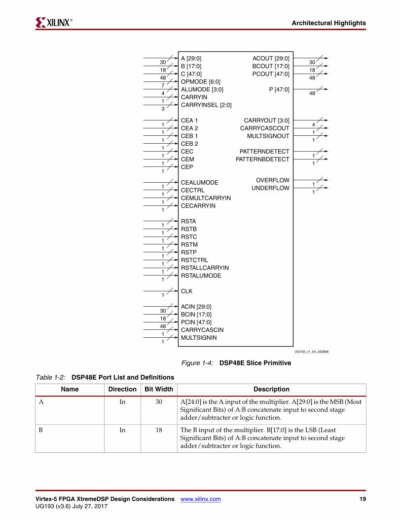
DSP48E Slice PrimitiveFigure 1-4 shows the DSP48E primitive. The figure also shows the input and output ports of the DSP48E slice along with the bit width of each port. The port list and definitions are in Table 1-2.
Table 1-1: Number of DSP48E Slices per Family Member
Device DSP Number of DSP48E per DeviceNumber of DSP48E Columns
per Device
XC5VLX30 32 1
XC5VLX50 48 1
XC5VLX85 48 1
XC5VLX110 64 1
XC5VLX155 128 2
XC5VLX220 128 2
XC5VLX330 192 2
XC5VLX20T 24 1
XC5VLX30T 32 1
XC5VLX50T 48 1
XC5VLX85T 48 1
XC5VLX110T 64 1
XC5VLX155T 128 2
XC5VLX220T 128 2
XC5VLX330T 192 2
XC5VSX35T 192 6
XC5VSX50T 288 6
XC5VSX95T 640 10
XC5VSX240T 1056 11
XC5VFX30T 64 2
XC5VFX70T 128 2
XC5VFX100T 256 4
XC5VFX130T 320 4
XC5VFX200T 384 4
XC5VTX150T 80 1
XC5VTX240T 96 1
Virtex-5 FPGA XtremeDSP Design Considerations www.xilinx.com 19UG193 (v3.6) July 27, 2017
Architectural HighlightsR
Figure 1-4: DSP48E Slice Primitive
A [29:0]B [17:0]C [47:0]OPMODE [6:0]ALUMODE [3:0]CARRYINCARRYINSEL [2:0]
CEA 1CEA 2CEB 1CEB 2CECCEMCEP
RSTARSTB
ACOUT [29:0]BCOUT [17:0]PCOUT [47:0]
P [47:0]
CARRYOUT [3:0]CARRYCASCOUT
MULTSIGNOUT
PATTERNDETECTPATTERNBDETECT
OVERFLOWUNDERFLOW
RSTC RSTMRSTPRSTCTRLRSTALLCARRYIN
CLK
RSTALUMODE
ACIN [29:0]BCIN [17:0]PCIN [47:0]CARRYCASCINMULTSIGNIN
CEALUMODECECTRLCEMULTCARRYINCECARRYIN
30
18
48
30
18
48
48
7
4
1
3
1
1
1
1
1
1
4
1
1
1
1
1
1
1
1
1
1
1
1
1
1
1
30
18
48
1
1
1
1
1
1
1
UG193_c1_04_032806
Table 1-2: DSP48E Port List and Definitions
Name Direction Bit Width Description
A In 30 A[24:0] is the A input of the multiplier. A[29:0] is the MSB (Most Significant Bits) of A:B concatenate input to second stage adder/subtracter or logic function.
B In 18 The B input of the multiplier. B[17:0] is the LSB (Least Significant Bits) of A:B concatenate input to second stage adder/subtracter or logic function.

20 www.xilinx.com Virtex-5 FPGA XtremeDSP Design ConsiderationsUG193 (v3.6) July 27, 2017
Chapter 1: DSP48E Description and SpecificsR
C In 48 Data input to second stage adder/subtracter, pattern detector, or logic function.
OPMODE In 7 Controls the input to the X,Y, and Z multiplexers in the DSP48E slice. (See Table 1-6, Table 1-7, and Table 1-8.)
ALUMODE In 4 Controls the selection of the logic function in the DSP48E slice. (See Table 1-12.)
CARRYIN In 1 Carry input from fabric.
CARRYINSEL In 3 Selects carry source (see Table 1-10).
CEA1 In 1 Clock enable for first A (input) register - only used if AREG = 2.
CEA2 In 1 Clock enable for second A (input) register - only used if AREG = 1 or 2.
CEB1 In 1 Clock enable for first B (input) register - only used if BREG = 2.
CEB2 In 1 Clock enable for second B (input) register - only used if BREG = 1 or 2.
CEC In 1 Clock enable for C (input) register.
CEM In 1 Clock enable for M (pipeline) register.
CEP In 1 Clock enable for P (output) register.
CECTRL In 1 Clock enable for OPMODE and CARRYINSEL (control inputs) registers.
CECARRYIN In 1 Clock enable for CARRYIN (input from fabric) register.
CEALUMODE In 1 Clock enable for ALUMODE (control inputs) registers.
CEMULTCARRYIN In 1 Clock enable for Carry (internal path) register (for multiplier only).
RSTA In 1 Reset for both A (input) registers.
RSTB In 1 Reset for both B (input) registers.
RSTC In 1 Reset for C (input) register.
RSTM In 1 Reset for M (pipeline) register.
RSTP In 1 Reset for P (output) register.
RSTCTRL In 1 Reset for OPMODE and CARRYINSEL (control inputs) registers.
RSTALLCARRYIN In 1 Reset for Carry (internal path) and CARRYIN register.
RSTALUMODE In 1 Reset for ALUMODE (control inputs) registers.
CLK In 1 The DSP48E input clock, common to all internal registers and flip-flops.
ACIN(1) In 30 Cascaded data input from ACOUT of previous DSP48E slice (muxed with A).
Table 1-2: DSP48E Port List and Definitions (Cont’d)
Name Direction Bit Width Description

Virtex-5 FPGA XtremeDSP Design Considerations www.xilinx.com 21UG193 (v3.6) July 27, 2017
Simplified DSP48E Slice OperationR
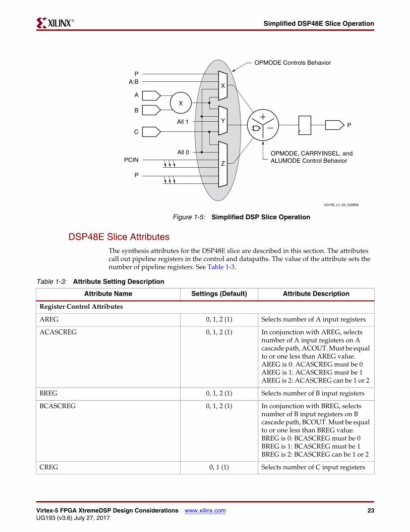
Simplified DSP48E Slice OperationThe math portion of the DSP48E slice consists of a 25-bit by 18-bit, two's complement multiplier followed by three 48-bit datapath multiplexers (with outputs X, Y, and Z). This is followed by a three-input adder/subtracter or two-input logic unit (see Figure 1-5). When using two-input logic unit, the multiplier cannot be used.
The data and control inputs to the DSP48E slice feed the arithmetic and logic stages. The A and B data inputs can optionally be registered one or two times to assist the construction of
BCIN(1) In 18 Cascaded data input from BCOUT of previous DSP48E slice (muxed with B).
PCIN(1) In 48 Cascaded data input from PCOUT of previous DSP48E slice to adder.
CARRYCASCIN(1) In 1 Cascaded carry input from CARRYCASCOUT of previous DSP48E slice.
MULTSIGNIN(1) In 1 Sign of the multiplied result from the previous DSP48E slice for MACC extension.
ACOUT(1) Out 30 Cascaded data output to ACIN of next DSP48E slice.
BCOUT(1) Out 18 Cascaded data output to BCIN of next DSP48E slice.
CARRYCASCOUT(1) Out 1 Cascaded carry output to CARRYCASCIN of next DSP48E slice. This signal is internally fed back into the CARRYINSEL multiplexer input of the same DSP48E slice.
MULTSIGNOUT(1) Out 1 Sign of the multiplied result cascaded to the next DSP48E slice for MACC extension.
P Out 48 Data output from second stage adder/subtracter or logic function.
PATTERNBDETECT Out 1 Output indicating a match between P[47:0] and pattern bar.
PATTERNDETECT Out 1 Output indicating a match between P[47:0] and pattern.
OVERFLOW Out 1 Output indicating overflow when used with appropriate setting of the pattern detector.
UNDERFLOW Out 1 Output indicating underflow when used with appropriate setting of the pattern detector.
CARRYOUT Out 4 4-bit CARRYOUT from each 12-bit section of logic unit/adder. Useful for SIMD.
CARRYOUT[3] is the carryout of the 48-bit adder (invalid during multiplies).
PCOUT(1) Out 48 Cascaded data output to PCIN of next DSP48E slice.
Notes: 1. These signals are dedicated routing paths internal to the DSP48E column. They are not accessible via fabric routing resources.2. All signals are active High.
Table 1-2: DSP48E Port List and Definitions (Cont’d)
Name Direction Bit Width Description

22 www.xilinx.com Virtex-5 FPGA XtremeDSP Design ConsiderationsUG193 (v3.6) July 27, 2017
Chapter 1: DSP48E Description and SpecificsR
different, highly pipelined, DSP application solutions. The other data inputs and the control inputs can be optionally registered once. Full speed operation is 550 MHz when using the pipeline registers. More detailed timing information is available in Chapter 2, “DSP48E Design Considerations.”
In its most basic form, the output of the adder/subtracter/logic unit is a function of its inputs. The inputs are driven by the upstream multiplexers, carry select logic, and multiplier array.
Equation 1-1 summarizes the combination of X, Y, Z, and CIN by the adder/subtracter. The CIN, X multiplexer output, and Y multiplexer output are always added together. This combined result can be selectively added to or subtracted from the Z multiplexer output. Note that the second option is a new feature of the DSP48E slice and is obtained by setting the ALUMODE to 0001.
Adder/Sub Out = (Z ± (X + Y + CIN)) or (-Z + (X + Y + CIN) –1) Equation 1-1
A typical use of the slice is where A and B inputs are multiplied and the result is added to or subtracted from the C register. More detailed operations based on control and data inputs are described in later sections. Selecting the multiplier function consumes both X and Y multiplexer outputs to feed the adder. The two 43-bit partial products from the multiplier are sign extended to 48 bits before being sent to the adder/subtracter.
When not using the first stage multiplier, the 48-bit, dual input, bit-wise logic function implements AND, OR, NOT, NAND, NOR, XOR, and XNOR. The inputs to these functions are A:B, C, P, or PCIN selected through the X and Z multiplexers, with the Y multiplexer selecting either all 1s or all 0s depending on logic operation.
The output of the adder/subtracter or logic unit feeds the pattern detector logic. The pattern detector allows the DSP48E slice to support Convergent Rounding, Counter Autoreset when a count value has been reached, and Overflow/Underflow/Saturation in accumulators. In conjunction with the logic unit, the pattern detector can be extended to perform a 48-bit dynamic comparison of two 48-bit fields. This enables functions such as A:B NAND C = = 0, or A:B (bit-wise logic) C = = Pattern to be implemented.
Figure 1-5 shows the DSP48E slice in a very simplified form. The seven OPMODE bits control the selects of X, Y, and Z multiplexers, feeding the inputs to the adder/subtracter or logic unit. In all cases, the 43-bit partial product data from the multiplier to the X and Y multiplexers is sign extended, forming 48-bit input datapaths to the adder/subtracter. Based on 43-bit operands and a 48-bit accumulator output, the number of “guard bits” (i.e., bits available to guard against overflow) is 5. Therefore, the number of multiply accumulations (MACC) possible before overflow occurs is 32. To extend the number of MACC operations, the MACC_EXTEND feature should be used, which allows the MACC to extend to 96 bits with two DSP48E slices. If A port is limited to 18 bits (sign-extended to 25), then there are 12 “guard bits” for the MACC, just like the Virtex-4 DSP48 slice. The CARRYOUT bits are invalid during multiply operations. Combinations of OPMODE, ALUMODE, CARRYINSEL, and CARRYIN control the function of the adder/subtracter or logic unit.
Virtex-5 FPGA XtremeDSP Design Considerations www.xilinx.com 23UG193 (v3.6) July 27, 2017
Simplified DSP48E Slice OperationR
DSP48E Slice AttributesThe synthesis attributes for the DSP48E slice are described in this section. The attributes call out pipeline registers in the control and datapaths. The value of the attribute sets the number of pipeline registers. See Table 1-3.
Figure 1-5: Simplified DSP Slice Operation
X
Y
OPMODE, CARRYINSEL, andALUMODE Control Behavior
X
P
P
A:B
A
B
C
PCINAll 0
P
Z
UG193_c1_05_032806
OPMODE Controls Behavior
All 1
Table 1-3: Attribute Setting Description
Attribute Name Settings (Default) Attribute Description
Register Control Attributes
AREG 0, 1, 2 (1) Selects number of A input registers
ACASCREG 0, 1, 2 (1) In conjunction with AREG, selects number of A input registers on A cascade path, ACOUT. Must be equal to or one less than AREG value. AREG is 0: ACASCREG must be 0 AREG is 1: ACASCREG must be 1 AREG is 2: ACASCREG can be 1 or 2
BREG 0, 1, 2 (1) Selects number of B input registers
BCASCREG 0, 1, 2 (1) In conjunction with BREG, selects number of B input registers on B cascade path, BCOUT. Must be equal to or one less than BREG value. BREG is 0: BCASCREG must be 0 BREG is 1: BCASCREG must be 1 BREG is 2: BCASCREG can be 1 or 2
CREG 0, 1 (1) Selects number of C input registers

24 www.xilinx.com Virtex-5 FPGA XtremeDSP Design ConsiderationsUG193 (v3.6) July 27, 2017
Chapter 1: DSP48E Description and SpecificsR
MREG 0, 1 (1) Selects number of M pipeline registers
PREG 0, 1 (1) Selects number of P output registers (also used by CARRYOUT/ PATTERN_DETECT/ CARRYCASCOUT/ MULTSIGNOUT, etc.)
OPMODEREG 0, 1 (1) Selects number of OPMODE input registers
ALUMODEREG 0, 1 (1) Selects number of ALUMODE input registers
CARRYINREG 0, 1 (1) Selects number of fabric CARRYIN input registers
MULTCARRYINREG 0, 1 (1) Selects number of Internal Carry registers (used for Multiply Symmetric Rounding only)
CARRYINSELREG 0, 1 (1) Selects number of CARRYINSEL input registers
Feature Control Attributes
A_INPUT DIRECT, CASCADE (DIRECT)
Selects the input to the A port between parallel input (DIRECT) or the cascaded input from the previous slice (CASCADE).
B_INPUT DIRECT, CASCADE (DIRECT)
Selects the input to the B port between parallel input (DIRECT) or the cascaded input from the previous slice (CASCADE).
Table 1-3: Attribute Setting Description (Cont’d)
Attribute Name Settings (Default) Attribute Description

Virtex-5 FPGA XtremeDSP Design Considerations www.xilinx.com 25UG193 (v3.6) July 27, 2017
Simplified DSP48E Slice OperationR
USE_MULT NONE, MULT, MULT_S (MULT_S)
Selects usage of the Multiplier in the DSP48E slice. The attribute should be set to NONE to save power when statically bypassing the multiplier, but NONE should not be used if the multiplier is dynamically bypassed with OPMODE control.
The MULT setting is used when the multiplier is configured as a non-pipelined multiplier. The MREG attribute must be set to 0 when the MULT setting is used. This setting is backward compatible to MULT18 x 18.
In the MULT_S setting, the MREG attribute must be set to 1. This setting is used when the multiplier is configured as a pipelined multiplier. This setting is backward compatible to MULT18 x 18S.
These settings help to port the MULT18 x 18 and MULT18 x 18S designs from a Virtex-4 design to a Virtex-5 implementation. This attribute replaces LEGACY_MODE. All previous modes of LEGACY_MODE and DRC checks are supported by USE_MULT.
USE_SIMD ONE48, TWO24,FOUR12 (ONE48)
Selects the mode of operation for the adder/subtracter. The attribute setting can be one 48-bit adder mode (ONE48), two 24-bit adder mode (TWO24), or four 12-bit adder mode (FOUR12). Selecting ONE48 mode is compatible with Virtex-4 DSP48 operation and is not actually a true SIMD mode. Typical Multiply-Add operations are supported when the mode is set to ONE48.
When either TWO24 or FOUR12 mode is selected, the multiplier must not be used, and USE_MULT must be set to NONE.
Table 1-3: Attribute Setting Description (Cont’d)
Attribute Name Settings (Default) Attribute Description

26 www.xilinx.com Virtex-5 FPGA XtremeDSP Design ConsiderationsUG193 (v3.6) July 27, 2017
Chapter 1: DSP48E Description and SpecificsR
Pattern Detector Attributes (see also “Pattern Detect Logic,” page 41)
PATTERN 48-bit field ("00…00") 48-bit value that is used in the pattern detector.
MASK 48-bit field ("0011...11") 48-bit value and used to mask out certain bits during a pattern detection. A value of 0 passes the bit, and a value of 1 masks out the bit.
SEL_PATTERN PATTERN, C (PATTERN)
Selects the input source for the pattern field. The input source can either be a 48-bit dynamic “C” input or a 48-bit static attribute field.
SEL_MASK MASK, C (MASK) Selects the input source for the mask field. The input source can either be a 48-bit dynamic “C” input or a 48-bit static attribute field.
SEL_ROUNDING_MASK SEL_MASK, MODE1, MODE2 (SEL_MASK)
Selects special masks that can be used for symmetric or convergent rounding uses of the pattern detector. This attribute takes precedence over the SEL_MASK attribute.
AUTORESET_PATTERN_DETECT_OPTINV MATCH, NOT_MATCH (MATCH)
Set true polarity of pattern detector as condition for resetting (MATCH).
Set complement polarity of pattern detector as condition for resetting (NOT_MATCH).
AUTORESET_PATTERN_DETECT TRUE, FALSE (FALSE) Reset P registers on next cycle if pattern is detected (TRUE); do not reset P register on the next cycle if pattern is detected (FALSE).
USE_PATTERN_DETECT NO_PATDET, PATDET (NO_PATDET)
If the pattern detector and related features are used (PATDET) or not used (NO_PATDET). This attribute is used for speed specification and Simulation Model purposes only.
Table 1-3: Attribute Setting Description (Cont’d)
Attribute Name Settings (Default) Attribute Description
Table 1-4: Internal Register Description
Register Description and Associated Attribute
2-Deep A Registers Two optional registers for the A input. Selected by AREG, enabled by CEA1 and CEA2 respectively, and reset synchronously by RSTA.
2-Deep B Registers Two optional registers on the B input. Selected by BREG, enabled by CEB1 and CEB2 respectively, and reset synchronously by RSTB.

Virtex-5 FPGA XtremeDSP Design Considerations www.xilinx.com 27UG193 (v3.6) July 27, 2017
Simplified DSP48E Slice OperationR
Input PortsThe ACIN, ALUMODE, CARRYCASCIN, MULTSIGNIN, along with the corresponding clock enable inputs and reset inputs, are new ports, introduced in the Virtex-5 family. The following section describes the input ports of the Virtex-5 DSP48E slice in detail. The input ports of the DSP48E slice are highlighted in Figure 1-6.
C Register Optional register for the C input, which is selected by CREG, enabled by CEC, and reset synchronously by RSTC.
M Register Optional pipeline register for output of multiplier, which consists of two 43-bit partial products.
These two partial products are input into X and Y multiplexers and finally into the adder/subtracter to create product output.
The M register is selected by MREG, enabled by CEM, and reset synchronously by RSTM.
OPMODE Register Optional pipeline register for the OPMODE control signal, which is selected by OPMODEREG, enabled by CECTRL, and reset synchronously by RSTCTRL.
CARRYINSEL Register Optional pipeline register for the CARRYINSEL control signal, which is selected by CARRYINSELREG, enabled by CECTRL, and reset synchronously by RSTCTRL.
ALUMODE Register Optional pipeline register for the ALUMODE control signal, which is selected by ALUMODEREG, enabled by CEALUMODE, and reset synchronously by RSTALUMODE
CARRYIN Register Optional pipeline register for the CARRYIN control signal, which is selected by CARRYINREG, enabled by CECARRYIN, reset synchronously by RSTALLCARRYIN.
Internal Mult Carry Register
Optional pipeline register for the Internal Carry signal (Used for Multiply Symmetric Rounding Only), which is selected by MULTCARRYINREG, enabled by CEMULTCARRYIN, and reset synchronously by RSTALLCARRYIN.
Output Registers Optional register for the P, OVERFLOW, UNDERFLOW, PATTERNDETECT, PATTERNDETECT, and CARRYOUT outputs, selected by PREG, enabled by CEP, and reset synchronously by RSTP. The same register also clocks out PCOUT, CARRYCASCOUT, and MULTSIGNOUT, which are the cascade outputs to the
next DSP48E slice.
Table 1-4: Internal Register Description (Cont’d)
Register Description and Associated Attribute

28 www.xilinx.com Virtex-5 FPGA XtremeDSP Design ConsiderationsUG193 (v3.6) July 27, 2017
Chapter 1: DSP48E Description and SpecificsR
A, B, and C Ports
The DSP48E slice input data ports support many common DSP and math algorithms. The DSP48E slice has three direct input data ports labeled A, B, and C. The A data port is 30 bits wide, the B data port is 18 bits wide, and the C data port is 48 bits wide. In Virtex-5 devices, each DSP48E slice also has an independent C data port. In Virtex-4 devices, the C port was shared between two DSP48 slices in a tile.
The 25-bit A (A[24:0]) and 18-bit B ports supply input data to the 25-bit by 18-bit, two's complement multiplier. With independent C port, each DSP48E slice is capable of Multiply-Add, Multiply-Subtract, and Multiply-Round operations.
Concatenated A and B ports bypass the multiplier and feed the X multiplexer input. The 30-bit A input port forms the upper 30-bits of A:B concatenated datapath, and the 18-bit B input port forms the lower 18 bits of the A:B datapath. The A:B datapath, together with the C input port, enables each DSP48E slice to implement a full 48-bit adder/subtracter provided the multiplier is not used.
Each DSP48E slice also has two cascaded input datapaths (ACIN and BCIN), providing a cascaded input stream between adjacent DSP48E slices. The cascaded path is 30 bits wide for the A input and 18 bits wide for the B input. Applications benefiting from this feature include FIR filters, complex multiplication, multi-precision multiplication and complex MACCs.
The A and B input port and the ACIN and BCIN cascade port can have 0, 1, or 2 pipeline stages in its datapath. The A and B port logic is shown in Figure 1-7. The different pipe stages are set using attributes. Attributes AREG and BREG are used to select the number of pipeline stages for A and B direct inputs. Attributes ACASCREG and BCASCREG select
Figure 1-6: Input Ports in DSP48E Slice
X
17-Bit Shift
17-Bit Shift
0
Y
Z
10
0
48
48
18
4
3
48
2530
BCOUT*
BCIN* ACIN*
OPMODE
PCIN*
MULTSIGNIN*
PCOUT*
CARRYCASCOUT*
MULTSIGNOUT*
CARRYCASCIN*CARRYIN
CARRYINSEL
ACOUT* A:B
ALUMODE
B
B
A
C
B
M
P
PP
C
25 X 18
A A
CREG/C Bypass/Mask
PATTERNDETECT
PATTERNBDETECT
CARRYOUT
UG193_c1_06_071206
4
7
48
4830
18
30
18
P
P
*These signals are dedicated routing paths internal to the DSP48E column. They are not accessible via fabric routing resources.
18

Virtex-5 FPGA XtremeDSP Design Considerations www.xilinx.com 29UG193 (v3.6) July 27, 2017
Simplified DSP48E Slice OperationR
the number of pipeline stages in the ACOUT and BCOUT cascade datapaths. The allowed attribute settings are shown in Table 1-3. Multiplexers controlled by configuration bits select flow through paths, optional registers, or cascaded inputs. The data port registers allow users to typically trade off increased clock frequency (i.e., higher performance) vs. data latency. The attribute settings for A and B port registers are listed in Table 1-5.
The 48-bit C port is used as a general input to the Y and Z multiplexer to perform add, subtract, three-input add/subtract, and logic functions. The C input is also connected to the pattern detector for rounding function implementations. The C port logic is shown in Figure 1-8. Attribute CREG is used to select the number of pipestages for the C input datapath.
Figure 1-7: A and B Input Port Logic
RSTDCE
RST
ACOUT/BCOUT
A/B
ACIN/BCIN
CE1
RSTDCE
RST
CE2
To MULT
UG193_c1_07_032806
Table 1-5: Attribute Setting for A and B Port Registers
Pipeline RegistersNotes
(Refer to Figure 1-7)AREG, BREG ACASCREG,BCASCREG
Current DSP To Cascade DSP
0 0 Direct and cascade paths have no registers.
1 1 Direct and cascade paths have one register.
2 1, 2 When direct path has two registers, cascade path can have one or two registers.
Note: If AREG = 1, then CEA2 is the only clock enable pin that is allowed to be used. If AREG = 0, then neither CEA1 nor CEA2 should be used. If AREG=2, then CEA1 and CEA2 can be used where CEA2 is the clock enable for the second register. This holds true for BREG and CEB1/CEB2 enable pins.

30 www.xilinx.com Virtex-5 FPGA XtremeDSP Design ConsiderationsUG193 (v3.6) July 27, 2017
Chapter 1: DSP48E Description and SpecificsR
OPMODE, ALUMODE, and CARRYINSEL Port Logic
The OPMODE, ALUMODE, and CARRYINSEL port logic supports flow through or registered input control signals. Multiplexers controlled by configuration bits select flow through or optional registers. The control port registers allow users to trade off increased clock frequency (i.e., higher performance) vs. data latency. The registers have independent clock enables and resets. The OPMODE and CARRYINSEL registers are reset by RSTCTRL. The ALUMODE is reset by RSTALUMODE. The clock enables and the OPMODE, ALUMODE, and CARRYINSEL port logic are shown in Figure 1-9.
Figure 1-8: C Port Logic
DEN
RST
CEC
RSTC
C C Input toY and Z Multiplexers and Pattern Detector
48
UG193_c1_08_032806
48
48
Figure 1-9: OPMODE, ALUMODE, and CARRYINSEL Port Logic
DEN
RST
CECTRL
RSTCTRL
OPMODE To the X, Y, ZMultiplexers and3-Input Adder/Subtracter
7
UG193_c1_09_092106
7
1
DEN
RST
CEALUMODE
RSTALUMODE
ALUMODE
To Adder/Subtracter4
4
1
1
DEN
RST
CARRYINSELTo Carry Input Select Logic
3
3
1

Virtex-5 FPGA XtremeDSP Design Considerations www.xilinx.com 31UG193 (v3.6) July 27, 2017
Simplified DSP48E Slice OperationR
X, Y, and Z Multiplexer
The OPMODE (Operating Mode) control input contains fields for X, Y, and Z multiplexer selects.
The OPMODE input provides a way for the user to dynamically change DSP48E functionality from clock cycle to clock cycle (e.g., when altering the internal datapath configuration of the DSP48E slice relative to a given calculation sequence).
The OPMODE bits can be optionally registered using the OPMODEREG attribute (as noted in Table 1-3).
Table 1-6, Table 1-7, and Table 1-8 list the possible values of OPMODE and the resulting function at the outputs of the three multiplexers (X, Y, and Z multiplexers). The multiplexer outputs supply three operands to the following adder/subtracter. Not all possible combinations for the multiplexer select bits are allowed. Some are marked in the tables as “illegal selection” and give undefined results. If the multiplier output is selected, then both the X and Y multiplexers are used to supply the multiplier partial products to the adder/subtracter.
If AREG/BREG = 0 and USE_MULT = MULT_S (this requires MREG=1), the A:B path should not be selected via the opmode multiplexer. Since the opmode can be dynamic, switching between the registered multiplier with MREG=1 and the combinatorial A:B path is not supported. If the multiplier is not being used, USE_MULT should be set to NONE.
Table 1-6: OPMODE Control Bits Select X Multiplexer Outputs
Z OPMODE [6:4]
YOPMODE [3:2]
XOPMODE [1:0]
X Multiplexer
OutputNotes
xxx xx 00 0 Default
xxx 01 01 M Must select with OPMODE[3:2]=01
xxx xx 10 P
xxx xx 11 A:B 48 bits wide
Table 1-7: OPMODE Control Bits Select Y Multiplexer Outputs
Z OPMODE[6:4]
YOPMODE[3:2]
XOPMODE[1:0]
Y Multiplexer
OutputNotes
xxx 00 xx 0 Default
xxx 01 01 M Must select with OPMODE[1:0]=01
xxx 10 xx 48'ffffffffffff Used mainly for logic unit bitwise operations on X and Z multiplexers
xxx 11 xx C

32 www.xilinx.com Virtex-5 FPGA XtremeDSP Design ConsiderationsUG193 (v3.6) July 27, 2017
Chapter 1: DSP48E Description and SpecificsR
ALUMODE Inputs
The 4-bit ALUMODE controls the behavior of the second stage add/sub/logic unit. ALUMODE = 0000 selects add operations of the form Z + (X + Y + CIN), which corresponds to Virtex-4 SUBTRACT = 0. ALUMODE = 0011 selects subtract operations of the form Z – (X + Y + CIN), which corresponds to Virtex-4 SUBTRACT = 1. ALUMODE set to 0001 can implement -Z + (X + Y + CIN) – 1. ALUMODE set to 0010 can implement -(Z + X + Y + CIN) – 1, which is equivalent to not (Z + X + Y + CIN). The negative of a two's complement number is obtained by performing a bitwise inversion and adding one,e.g., -k = not (k) + 1. Other subtract and logic operations can also be implemented with the enhanced add/sub/logic unit. See Table 1-9.
Also, see Table 1-12 for two-input ALUMODE operations and Figure A-3.
Table 1-8: OPMODE Control Bits Select Z Multiplexer Outputs
Z OPMODE[6:4]
Y OPMODE[3:2]
X OPMODE[1:0]
Z Multiplexer
OutputNotes
000 xx xx 0 Default
001 xx xx PCIN
010 xx xx P
011 xx xx C
100 10 00 P Use for MACC extend only
101 xx xx 17-bit Shift(PCIN)
110 xx xx 17-bit Shift(P)
111 xx xx xx Illegal selection
Table 1-9: Three-Input ALUMODE Operations
DSP Operation OPMODE [6:0]ALUMODE [3:0]
3 2 1 0
Z + X + Y + CARRYIN (Corresponds to SUBTRACT = 0 in Virtex-4 DSP48 slice)
Any legal OPMODE 0 0 0 0
Z – (X + Y + CARRYIN) (Corresponds to SUBTRACT = 1 in Virtex-4 DSP48 slice)
Any legal OPMODE 0 0 1 1
-Z + (X + Y + CARRYIN) – 1 = not (Z) + X + Y + CARRYIN
Any legal OPMODE 0 0 0 1
not (Z + X + Y + CARRYIN) = -Z – X – Y – CARRYIN - 1
Any legal OPMODE 0 0 1 0
Notes: 1. In two's complement: -Z = not (Z) + 1

Virtex-5 FPGA XtremeDSP Design Considerations www.xilinx.com 33UG193 (v3.6) July 27, 2017
Simplified DSP48E Slice OperationR
Carry Input Logic
In Virtex-5 devices, the carry input logic result is a function of a 3-bit-wide CARRYINSEL signal. The inputs to the carry input logic appear in Figure 1-10. Carry inputs used to form results for adders and subtracters are always in the critical path. High performance is achieved by implementing this logic in silicon. The possible carry inputs to the carry logic are “gathered” prior to the outputs of the X, Y, and Z multiplexers. In Virtex-5 devices, CARRYIN has no dependency on the OPMODE selection.
Figure 1-10 shows eight inputs selected by the 3-bit CARRYINSEL control.
The first input, CARRYIN (CARRYINSEL set to binary 000), is driven from general logic. This option allows implementation of a carry function based on user logic. CARRYIN can be optionally registered. The next input, (CARRYINSEL is equal to binary 010) is the CARRYCASCIN input from an adjacent DSP48E slice. The third input (CARRYINSEL is equal to binary 100) is the CARRYCASCOUT from the same DSP48E slice, fed back to itself.
The fourth input (CARRYINSEL is equal to binary 110) is A[24] XNOR B[17] for symmetrically rounding multiplier outputs. This signal can be optionally registered to match the MREG pipeline delay. The fifth and sixth inputs (CARRYINSEL is equal to binary 111 and 101)selects the true or inverted P output MSB P[47] for symmetrically rounding the P output. The seventh and eight inputs (CARRYINSEL is equal to binary 011 and 001)selects the true or inverted cascaded P input msb PCIN[47] for symmetrically rounding the cascaded P input.
Figure 1-10: CARRYINSEL Port Logic
RST
CED
RSTALLCARRYIN
CECARRYIN
CARRYCASCIN
Fabric CARRYIN
Large Add/Sub/Acc(Parallel Op)
Large Add/Sub/Acc(Seq Op)
UG193_c1_10_010906
000
010
100
110
111
101
011
001
CARRYCASCOUT
A[24] XNOR B[17]
Inverted P[47]
Inverted PCIN[47]
3
RST
CED
RSTALLCARRYIN
CEMULTCARRYIN
Round A * B
Round Output
CARRYINSEL
ADDER
34 www.xilinx.com Virtex-5 FPGA XtremeDSP Design ConsiderationsUG193 (v3.6) July 27, 2017
Chapter 1: DSP48E Description and SpecificsR
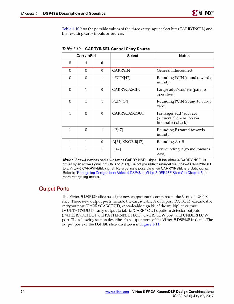
Table 1-10 lists the possible values of the three carry input select bits (CARRYINSEL) and the resulting carry inputs or sources.
Output PortsThe Virtex-5 DSP48E slice has eight new output ports compared to the Virtex-4 DSP48 slice. These new output ports include the cascadeable A data port (ACOUT), cascadeable carryout port (CARRYCASCOUT), cascadeable sign bit of the multiplier output (MULTSIGNOUT), carry output to fabric (CARRYOUT), pattern detector outputs (PATTERNDETECT and PATTERNBDETECT), OVERFLOW port, and UNDERFLOW port. The following section describes the output ports of the Virtex-5 DSP48E in detail. The output ports of the DSP48E slice are shown in Figure 1-11.
Table 1-10: CARRYINSEL Control Carry Source
CarryInSel Select Notes
2 1 0
0 0 0 CARRYIN General Interconnect
0 0 1 ~PCIN[47] Rounding PCIN (round towards infinity)
0 1 0 CARRYCASCIN Larger add/sub/acc (parallel operation)
0 1 1 PCIN[47] Rounding PCIN (round towards zero)
1 0 0 CARRYCASCOUT For larger add/sub/acc (sequential operation via internal feedback)
1 0 1 ~P[47] Rounding P (round towards infinity)
1 1 0 A[24] XNOR B[17] Rounding A x B
1 1 1 P[47] For rounding P (round towards zero)
Note: Virtex-4 devices had a 2-bit-wide CARRYINSEL signal. If the Virtex-4 CARRYINSEL is driven by an active signal (not GND or VCC), it is not possible to retarget the Virtex-4 CARRYINSEL to a Virtex-5 CARRYINSEL signal. Retargeting is possible when CARRYINSEL is a static signal. Refer to “Retargeting Designs from Virtex-4 DSP48 to Virtex-5 DSP48E Slices” in Chapter 5 for more retargeting details.

Virtex-5 FPGA XtremeDSP Design Considerations www.xilinx.com 35UG193 (v3.6) July 27, 2017
Simplified DSP48E Slice OperationR
All the output ports except ACOUT and BCOUT are reset by RSTP and enabled by CEP (see Figure 1-12). ACOUT and BCOUT are reset by RSTA and RSTB respectively (shown in Figure 1-7).
P Port
Each DSP48E slice has a 48-bit-wide output port P. This output can be connected (cascaded connection) to the adjacent DSP48E slice internally through the PCOUT path. The PCOUT connects to the input of the Z multiplexer (PCIN) in the adjacent DSP48E slice. This path provides an output cascade stream between adjacent DSP48E slices.
Figure 1-11: Output Ports in DSP48E Slice
X
17-Bit Shift
17-Bit Shift
0
Y
Z
10
0
48
48
18
4
3
48
2530
BCOUT*
BCIN* ACIN*
OPMODE
PCIN*
MULTSIGNIN*
PCOUT*
CARRYCASCOUT*
MULTSIGNOUT*
CREG/C Bypass/Mask
CARRYCASCIN*CARRYIN
CARRYINSEL
ACOUT* A:B
ALUMODE
B
B
A
C
B
M
P
PP
C
25 X 18
A A
PATTERNDETECT
PATTERNBDETECT
CARRYOUT
UG193_c1_11_013006
4
7
48
4830
18
30
18
P
P
*These signals are dedicated routing paths internal to the DSP48E column. They are not accessible via fabric routing resources.
Figure 1-12: Output Port Logic
DEN Q
RST
CEP
RSTP
P/PCOUT/MULTSIGNOUT/CARRYCASCOUT/
CARRYOUT/PATTERNDETECT/
PATTERNBDETECT
DSP48ESlice Output
UG193_c1_12_112907

36 www.xilinx.com Virtex-5 FPGA XtremeDSP Design ConsiderationsUG193 (v3.6) July 27, 2017
Chapter 1: DSP48E Description and SpecificsR
CARRYCASCOUT and CARRYOUT Ports
The carry out from each DSP48E slice can be sent to the fabric using the CARRYOUT port. This port is 4 bits wide. CARRYOUT[3] is the valid carry output for a two-input 48-bit adder/subtracter or one-input accumulator. In this case, USE_SIMD=ONE48 is the default setting and represents a non-SIMD configuration. When a two-input adder/subtracter or one-input accumulator is used in SIMD mode, such as TWO24 or FOUR12, the valid carry out signals are listed in Table 1-11. The carry out signals are not valid if three-input adder/subtracter (e.g., A:B + C + PCIN) or two-input accumulator (e.g., A:B + C + P) configurations are used or if the multiplier is used.
See also Table 1-9 for 3-input ALUMODE operations.
The CARRYOUT signal is cascaded to the next adjacent DSP48E slice using the CARRYCASCOUT port. Larger add, subtract, ACC, and MACC functions can be implemented in the DSP48E slice using the CARRYCASCOUT output port. The one bit CARRYCASCOUT signal corresponds to CARRYOUT[3], but is not identical. The CARRYCASCOUT signal is also fed back into the same DSP48E slice via the CARRYINSEL multiplexer.
The CARRYOUT[3] signal should be ignored when the multiplier or a ternary add/subtract operation is used. Because a MACC operation includes a three-input adder in the accumulator stage, the combination of MULTSIGNOUT and CARRYCASCOUT signals is required to perform a 96-bit MACC, spanning two DSP48E slices. The second DSP48E slice’s OPMODE must be MACC_EXTEND (1001000) to use both CARRYCASCOUT and MULTSIGNOUT, thereby eliminating the ternary adder carry restriction for the upper DSP48E slice. The actual hardware implementation of CARRYOUT/CARRYCASCOUT and the differences between them are described in Appendix A.
For more on the CARRYOUT, and MACC_EXTEND usage, refer to “Advanced Math Applications” in Chapter 4.
MULTSIGNOUT Port Logic
MULTSIGNOUT is a software abstraction of the actual hardware signal. It is modeled as the MSB of the multiplier output and used only in MACC extension applications to build a 96-bit MACC. This operation is described in Chapter 4, “Advanced Math Applications.” The actual hardware implementation of MULTSIGNOUT is described in Appendix A.
Table 1-11: Carryout Bit Associated with Different SIMD Mode
SIMD Mode Adder Bit Width Corresponding Carryout
FOUR12 P[11:0] CARRYOUT[0]
P[23:12] CARRYOUT[1]
P[35:24] CARRYOUT[2]
P[47:36] CARRYOUT[3]
TWO24 P[23:0] CARRYOUT[1]
P[47:24] CARRYOUT[3]
ONE48 P[47:0] CARRYOUT[3]

Virtex-5 FPGA XtremeDSP Design Considerations www.xilinx.com 37UG193 (v3.6) July 27, 2017
Simplified DSP48E Slice OperationR
The MSB of a multiplier output is cascaded to the next DSP48E slice using the /MULTSIGNIN port and can be used only in MACC extension applications to build a 96-bit accumulator. This opmode setting is described in Chapter 4, “Advanced Math Applications.” The actual hardware implementation of MULTSIGNOUT is described in the Appendix A.
PATTERNDETECT and PATTERNBDETECT Port Logic
A pattern detector has been added on the output of the DSP48E slice to detect if the P bus matches a specified pattern or if it exactly matches the complement of the pattern. The PATTERNDETECT (PD) output goes High if the output of the adder matches a set pattern. The PATTERNBDETECT (PBD) output goes High if the output of the adder matches the complement of the set pattern.
A mask field can also be used to hide certain bit locations in the pattern detector. The PATTERNDETECT computes ((P == pattern)||mask) on a bitwise basis and then ANDs the results to a single output bit. Similarly, the PATTERNBDETECT can detect if ((P == ~pattern)||mask). The pattern and the mask fields can each come from a distinct 48-bit configuration field or from the (registered) C input. When the C input is used as the PATTERN, the OPMODE should be set to select a '0' at the input of the Z multiplexer. If all the registers are reset, the PATTERNDETECT is High for one clock cycle immediately after the RESET is deasserted.
The pattern detector allows the DSP48E slice to support convergent rounding and counter auto reset when a count value has been reached as well as support overflow, underflow, and saturation in accumulators.
Overflow and Underflow Port Logic
The dedicated OVERFLOW and UNDERFLOW outputs of the DSP48E slice use the pattern detector to determine if the operation in the DSP48E slice has overflowed beyond the P[N] bit where N is between 1 and 46. The P register must be enabled while using overflow and underflow ports. This is further described in the “Embedded Functions”section.
Embedded FunctionsThe embedded functions in Virtex-5 devices include a 25 x 18 multiplier, adder/subtracter/logic unit, and pattern detector logic (see Figure 1-13).

38 www.xilinx.com Virtex-5 FPGA XtremeDSP Design ConsiderationsUG193 (v3.6) July 27, 2017
Chapter 1: DSP48E Description and SpecificsR
Two’s Complement Multiplier
The two's complement multiplier in the DSP48E slice in Figure 1-13 accepts a 25-bit two's complement input and an 18-bit two's complement input. The multiplier produces two 43-bit partial products. The two partial products together give an 86-bit result at the output of the multiplier, as shown in Figure 1-14. Cascading of multipliers to achieve larger products is supported with a 17-bit right-shifted cascaded output bus. The right shift is used to right justify the partial products by the correct number of bits. This cascade path feeds into the Z multiplexer, which is connected to the adder/subtracter of an adjacent DSP48E slice. The multiplier can emulate unsigned math by setting the MSB of an input operand to zero.
Figure 1-14 shows an optional pipeline register (MREG) for the output of the multiplier.
Using the register provides increased performance with an increase of one clock latency.
Figure 1-13: Embedded Functions in a DSP48E Slice
X
17-Bit Shift
17-Bit Shift
0
Y
Z
10
0
48
48
18
4
3
48
2530
BCOUT*
BCIN* ACIN*
OPMODE
PCIN*
MULTSIGNIN*
PCOUT*
CARRYCASCOUT*
MULTSIGNOUT*
CREG/C Bypass/Mask
CARRYCASCIN*CARRYIN
CARRYINSEL
ACOUT* A:B
ALUMODE
B
B
A
C
B
M
P
PP
C
25 X 18
A A
PATTERNDETECT
PATTERNBDETECT
CARRYOUT
UG193_c1_13_013006
4
7
48
4830
18
30
18
P
P
*These signals are dedicated routing paths internal to the DSP48E column. They are not accessible via fabric routing resources.
Figure 1-14: Two's Complement Multiplier Followed by Optional MREG
XA
Partial Product 1
Partial Product 2B
OptionalMREG
UG193_c1_14_120205
86
43
43

Virtex-5 FPGA XtremeDSP Design Considerations www.xilinx.com 39UG193 (v3.6) July 27, 2017
Simplified DSP48E Slice OperationR
Adder/Subtracter or Logic Unit
The adder/subtracter or logic unit output is a function of control and data inputs (see Figure 1-15). The data inputs to the adder/subtracter are selected by the OPMODE and the CarryInSel signals. The ALUMODE signals choose the function implemented in the adder/subtracter. Thus, the OPMODE, ALUMODE, and CARRYINSEL signals together determine the functionality of the embedded adder/subtracter/logic unit. When using the logic unit, the multiplier must not be used. The values of OPMODEREG and CARRYINSELREG must be identical.
As with the input multiplexers, the OPMODE bits specify a portion of this function. The symbol ± in the table means either add or subtract and is specified by the state of the ALUMODE control signal (ALUMODE = 0011 is defined as “subtraction,” used for retargeting designs from Virtex-4 devices). The symbol “:” in the table means concatenation. The outputs of the X and Y multiplexer and CIN are always added together. Refer to “ALUMODE Inputs,” page 32.
Two Input Logic Unit
In Virtex-5 devices, the capability to perform an addition, subtraction, and simple logic functions in the DSP48E slice exists through use of a second-stage, three-input adder. To increase the versatility of the Virtex-4 DSP48 slice in applications where multipliers are not needed, logic is included in the second stage of the adder/subtracter to create a 48-bit logic unit.
Table 1-12 lists the logic functions that can be implemented in the second stage of the three input adder/subtracter/logic unit. The table also lists the settings of the control signals, namely OPMODE and ALUMODE.
Setting OPMODE[3:2] to "00" selects the default "0" value at the Y multiplexer output. OPMODE[3:2] set to "10" selects "all 1s" at the Y multiplexer output. OPMODE[1:0] selects the output of the X multiplexer, and OPMODE[6:4] selects the output of the Z multiplexer.
Table 1-12: OPMODE and ALUMODE Control Bits Select Logic Unit Outputs
Logic Unit ModeOpMode
<3:2>ALUMode
<3:0>
3 2 3 2 1 0
X XOR Z 0 0 0 1 0 0
X XNOR Z 0 0 0 1 0 1
X XNOR Z 0 0 0 1 1 0
X XOR Z 0 0 0 1 1 1
X AND Z 0 0 1 1 0 0
X AND (NOT Z) 0 0 1 1 0 1
X NAND Z 0 0 1 1 1 0
(NOT X) OR Z 0 0 1 1 1 1
X XNOR Z 1 0 0 1 0 0
X XOR Z 1 0 0 1 0 1

40 www.xilinx.com Virtex-5 FPGA XtremeDSP Design ConsiderationsUG193 (v3.6) July 27, 2017
Chapter 1: DSP48E Description and SpecificsR
Single Instruction, Multiple Data (SIMD) ModeThe 48-bit adder/subtracter/accumulator can be split into smaller data segments where the internal carry propagation between segments is blocked to ensure independent operation for all segments. The adder/subtracter/accumulator is capable of being split into four 12-bit adder/subtracter/accumulators or two 24-bit adder/subtracter/accumulators with carry out signal per segment. The SIMD mode segmentation is a static configuration as opposed to dynamic OPMODE type control (see Figure 1-15).
• Four segments of dual or ternary adders with 12-bit inputs, a 12-bit output, and a carry output for each segment
• Function controlled dynamically by ALUMODE[3:0], and operand source by OPMODE[6:0]
X XOR Z 1 0 0 1 1 0
X XNOR Z 1 0 0 1 1 1
X OR Z 1 0 1 1 0 0
X OR (NOT Z) 1 0 1 1 0 1
X NOR Z 1 0 1 1 1 0
(NOT X) AND Z 1 0 1 1 1 1
Table 1-12: OPMODE and ALUMODE Control Bits Select Logic Unit Outputs (Cont’d)
Logic Unit ModeOpMode
<3:2>ALUMode
<3:0>
3 2 3 2 1 0
Figure 1-15: Four 12-Bit SIMD Adder Configuration
X0
P
ALUMODE[3:0]
P[11:0], CARRYOUT[0]
P[23:12], CARRYOUT[1]
P[35:24], CARRYOUT[2]
P[47:36], CARRYOUT[3][47:0]
[47:0]
[47:36]
[35:24]
[23:12]
[11:0]
UG193_c1_15_032806
01
PCIN
P
C
Z
Y
A:B
C
0

Virtex-5 FPGA XtremeDSP Design Considerations www.xilinx.com 41UG193 (v3.6) July 27, 2017
Simplified DSP48E Slice OperationR
• All four adder/subtracter/accumulators perform same function
• Two segments of dual or ternary adders with 24-bit inputs, a 24-bit output, and a carry output for each segment is also available (not pictured).
The SIMD feature, shown in Figure 1-15, allows the 48-bit logic unit to be split into multiple smaller logic units. Each smaller logic unit performs the same function. This function can also be changed dynamically through the ALUMODE[3:0] and opmode control inputs.
Pattern Detect LogicThe pattern detector is connected to the output of the add/subtract/logic unit in the DSP48E slice (see Figure 1-13).
The pattern detector is best described as an equality check on the output of the adder/subtracter/logic unit that produces its result on the same cycle as the P output. There is no extra latency between the pattern detect output and the P output of the DSP48E slice. The use of the pattern detector leads to a moderate speed reduction due to the extra logic on the pattern detect path (see Figure 1-16).
Figure 1-16: Pattern Detector Logic
C (Register)
PATTERN
P
UG193_c1_16_071006
C (Register)
MASK
C Shift by 2, 00 (Mode 2)
C Shift by 1, 0 (Mode 1)
SEL_ROUNDING_MASK
PATTERNMASK
= 48’b00000000...= 48’b00111111...
SEL_MASK
SEL_PATTERN
PATTERNBDETECTPAST(1)
PATTERNBDETECT
PATTERNDETECT
P
PATTERNDETECTPAST(1)
Notes: (1) Denotes an internal signal
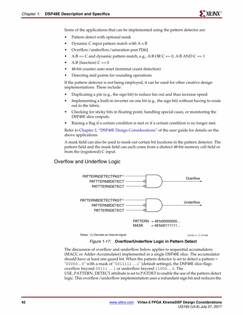
42 www.xilinx.com Virtex-5 FPGA XtremeDSP Design ConsiderationsUG193 (v3.6) July 27, 2017
Chapter 1: DSP48E Description and SpecificsR
Some of the applications that can be implemented using the pattern detector are:
• Pattern detect with optional mask
• Dynamic C input pattern match with A x B
• Overflow/underflow/saturation past P[46]
• A:B == C and dynamic pattern match, e.g., A:B OR C == 0, A:B AND C == 1
• A:B {function} C == 0
• 48-bit counter auto reset (terminal count detection)
• Detecting mid points for rounding operations
If the pattern detector is not being employed, it can be used for other creative design implementations. These include:
• Duplicating a pin (e.g., the sign bit) to reduce fan out and thus increase speed.
• Implementing a built-in inverter on one bit (e.g., the sign bit) without having to route out to the fabric.
• Checking for sticky bits in floating point, handling special cases, or monitoring the DSP48E slice outputs.
• Raising a flag if a certain condition is met or if a certain condition is no longer met.
Refer to Chapter 2, “DSP48E Design Considerations” of the user guide for details on the above applications.
A mask field can also be used to mask out certain bit locations in the pattern detector. The pattern field and the mask field can each come from a distinct 48-bit memory cell field or from the (registered) C input.
Overflow and Underflow Logic
The discussion of overflow and underflow below applies to sequential accumulators (MACC or Adder-Accumulator) implemented in a single DSP48E slice. The accumulator should have at least one guard bit. When the pattern detector is set to detect a pattern = "00000…0" with a mask of "0011111 …1" (default settings), the DSP48E slice flags overflow beyond 00111 … 1 or underflow beyond 11000… 0. The USE_PATTERN_DETECT attribute is set to PATDET to enable the use of the pattern detect logic. This overflow/underflow implementation uses a redundant sign bit and reduces the
Figure 1-17: Overflow/Underflow Logic in Pattern Detect
PATTERNBDETECTPAST(1)
PATTERNBDETECTPATTERNDETECT
Underflow
PATTERNDETECTPAST(1)
PATTTERNBDETECTPATTTERNDETECT
Overflow
UG193_c1_17_071006
PATTERNMASK
= 48’b00000000...= 48’b00111111...
Notes: (1) Denotes an internal signal
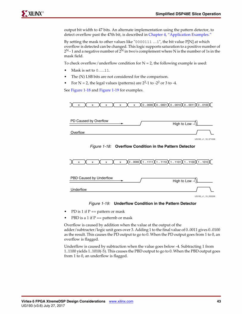
Virtex-5 FPGA XtremeDSP Design Considerations www.xilinx.com 43UG193 (v3.6) July 27, 2017
Simplified DSP48E Slice OperationR
output bit width to 47 bits. An alternate implementation using the pattern detector, to detect overflow past the 47th bit, is described in Chapter 4, “Application Examples.”
By setting the mask to other values like "0000111 …1", the bit value P[N] at which overflow is detected can be changed. This logic supports saturation to a positive number of 2N - 1 and a negative number of 2N in two's complement where N is the number of 1s in the mask field.
To check overflow/underflow condition for N = 2, the following example is used:
• Mask is set to 0…..11.
• The (N) LSB bits are not considered for the comparison.
• For N = 2, the legal values (patterns) are 22-1 to -22 or 3 to -4.
See Figure 1-18 and Figure 1-19 for examples.
• PD is 1 if P == pattern or mask
• PBD is a 1 if P == patternb or mask
Overflow is caused by addition when the value at the output of the adder/subtracter/logic unit goes over 3. Adding 1 to the final value of 0..0011 gives 0..0100 as the result. This causes the PD output to go to 0. When the PD output goes from 1 to 0, an overflow is flagged.
Underflow is caused by subtraction when the value goes below -4. Subtracting 1 from 1..1100 yields 1..1010(-5). This causes the PBD output to go to 0. When the PBD output goes from 1 to 0, an underflow is flagged.
Figure 1-18: Overflow Condition in the Pattern Detector
Figure 1-19: Underflow Condition in the Pattern Detector
x x x x x 0 .. 0000 0 .. 0001 0 .. 0010 0 .. 0011 0 .. 0100
PD Caused by Overflow
UG193_c1_18_071006
High to Low
Overflow
x x x x 1 .. 1111 1 .. 1110 1 .. 1101 1 .. 1100 1 .. 1010
PBD Caused by Underflow
UG193_c1_19_052206
High to Low
Underflow
0 .. 0000

44 www.xilinx.com Virtex-5 FPGA XtremeDSP Design ConsiderationsUG193 (v3.6) July 27, 2017
Chapter 1: DSP48E Description and SpecificsR
Auto Reset Logic
After a count value is reached without extra fabric logic, an auto reset is provided in the DSP48E slice to automatically reset the DSP48 PREG (and pattern_detect REG). This is useful in building large N-bit counters for finite state machines, cycling filter coefficients, etc. The auto reset logic is shown in Figure 1-20.
Two attributes are associated with using the auto reset logic. If the AUTORESET_PATTERN_DETECT attribute is set to TRUE and the AUTORESET_PATTERN_DETECT_OPTINV is set to MATCH, then the PREG attribute automatically resets the P register one clock cycle after a pattern has been detected. For example, DSP resets when 00001000 is detected. To get a repeating 9-state counter from 0 to 8, a 1 is repeatedly added to the DSP slice.
If the AUTORESET_PATTERN_DETECT attribute is set to TRUE and AUTORESET_POLARITY is set to NOT_MATCH, then the P register auto resets on the next clock cycle only if a pattern was detected - but is now no longer detected. For example, DSP resets if 00000XXX is no longer detected (set PATTERN = 000...01000, and MASK = 000...00000). A 1 is repeatedly added to the DSP to get a repeating 9-state counter from 0 to 8. This mode of counter can be useful if different numbers are added on every cycle and a reset is triggered every time a threshold (must be a power of 2) is crossed.
Figure 1-20: Auto Reset Logic
“OR” withExternal RSTP
UG193_c1_20_032806
PATTERNDETECT
AUTORESET_PATTERN_DETECT_OPTINV
PATTERNDETECTPAST
PATTERNDETECT
AUTORESET_PATTERN_DETECT

Virtex-5 FPGA XtremeDSP Design Considerations www.xilinx.com 45UG193 (v3.6) July 27, 2017
R
Chapter 2
DSP48E Design Considerations
IntroductionThis chapter describes some of the design features and techniques to use in order to achieve higher performance, lower power, and lower resources in a particular design.
Designing for Performance (to 550 MHz)To get the maximum performance out of the DSP48E slices, it is desirable to use all the pipeline stages within the slice. To achieve maximum performance when using the DSP48E slice, the design needs to be fully pipelined. For multiplier-based designs, the DSP48E slice requires a three-stage pipeline. For non-multiplier-based designs, a two-stage pipeline should be used. The performance impact of including the different registers within a DSP48E slice is given in Chapter 3, “DSP48E Timing Consideration.” Also see DS202, Virtex-5 FPGA Data Sheet: DC and Switching Characteristics. If latency is important in the design and only one or two registers can be used within the DSP48E slice, always use the M register.
Designing for PowerThe USE_MULT attribute selects usage of the Multiplier. This attribute should be set to NONE to save power when using only the Adder/Logic Unit. Functions implemented in the DSP48E slice use less power than those implemented in fabric. Using the cascade paths within the DSP48E slice instead of fabric routing is another way to reduce power. A multiplier with the M register turned on uses less power than one where the M register is not used. For operands less than 25 x 18, fabric power can be reduced by placing operands into the MSBs and zero padding unused LSBs.
Adder Tree vs. Adder Chain
Adder TreeIn typical direct form FIR filters, an input stream of samples is presented to one input of the multipliers in the DSP48E slices. The coefficients supply the other input to the multipliers. An adder tree is used to combine the outputs from many multipliers as shown in Figure 2-1.

46 www.xilinx.com Virtex-5 FPGA XtremeDSP Design ConsiderationsUG193 (v3.6) July 27, 2017
Chapter 2: DSP48E Design ConsiderationsR
In traditional FPGAs, the fabric adders are usually the performance bottleneck. The number of adders needed and the associated routing depends on the size of the filter. The depth of the adder tree scales as the log2 of the number of taps in the filter. Using the adder tree structure shown in Figure 2-1 could also increase the cost, logic resources, and power.
The CLB architecture in Virtex®-5 devices improves the performance of the final adder tree carry chains by approximately 32%. The Virtex-5 CLB allows the use of both the 6LUT and the carry chain in the same slice to build an efficient ternary adder. The 6LUT in the CLB functions as a dual 5LUT. The 5LUT is used as a 3:2 compressor to add three input values to produce two output values. The 3:2 compressor is shown in Figure 2-2.
Figure 2-1: Traditional FIR Filter Adder Tree
48
48
y(n-6)
18
18 48
48
×
+
+ 18
18
18
18
18
18
h0(n)
X(n)
h1(n)
48
48
18
18 48
48
×
+ × 18
18
×
18
18
18
18
h2(n)
X(n)
h3(n)
h4(n)
X(n-2)
X(n-4)
h5(n)
h6(n)
h7(n)
+
+
Z-2
Z-2
Z-2
×
×
×
× +
The final stages of the post addition in logic are the performance bottleneck that consume more power.
ug193_c2_01_022706
+

Virtex-5 FPGA XtremeDSP Design Considerations www.xilinx.com 47UG193 (v3.6) July 27, 2017
Adder Tree vs. Adder ChainR
The dual 5LUT configured as a 3:2 compressor in combination with the 2-input carry cascade adder adds three N-bit numbers to produce one N+2 bit output, as shown in the Figure 2-3, by vertically stacking the required number of slices.
Figure 2-2: Ternary Add/Sub with 3:2 Compressor
X(1)Y(1)
Z(1)
BBUS(0)SUB/
ADDB
BBUS(0)
SUB/ADDB
SUB/ADDB
AX
A5
A2
A3A4
IN5
00 1
O6A
CY(0)
CY(1)
GND
O5A
1
VDD
IN6
IN2
DAQ
AMUX
SUM(0)
BBUS(0)
Q
CK
IN3IN4
X(0)Y(0)
Z(0)
BX
B5
B2
B3B4
IN5
B1 IN1
00 1
O6B
O5B
1
VDD
IN6
IN2
DBQ
BMUX
SUM(1)
BBUS(1)
Q
CK
IN3IN4 ABUS(1)
ABUS(0)
UG193_c2_02_010709
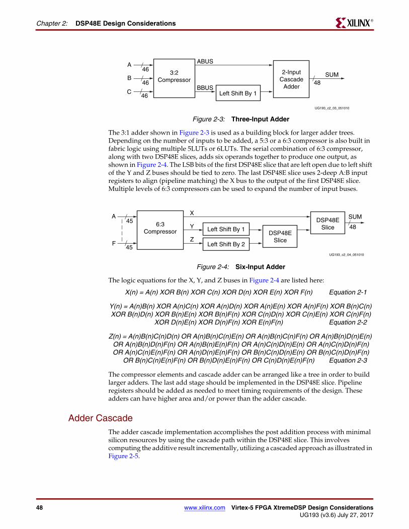
48 www.xilinx.com Virtex-5 FPGA XtremeDSP Design ConsiderationsUG193 (v3.6) July 27, 2017
Chapter 2: DSP48E Design ConsiderationsR
The 3:1 adder shown in Figure 2-3 is used as a building block for larger adder trees. Depending on the number of inputs to be added, a 5:3 or a 6:3 compressor is also built in fabric logic using multiple 5LUTs or 6LUTs. The serial combination of 6:3 compressor, along with two DSP48E slices, adds six operands together to produce one output, as shown in Figure 2-4. The LSB bits of the first DSP48E slice that are left open due to left shift of the Y and Z buses should be tied to zero. The last DSP48E slice uses 2-deep A:B input registers to align (pipeline matching) the X bus to the output of the first DSP48E slice. Multiple levels of 6:3 compressors can be used to expand the number of input buses.
The logic equations for the X, Y, and Z buses in Figure 2-4 are listed here:
X(n) = A(n) XOR B(n) XOR C(n) XOR D(n) XOR E(n) XOR F(n) Equation 2-1
Y(n) = A(n)B(n) XOR A(n)C(n) XOR A(n)D(n) XOR A(n)E(n) XOR A(n)F(n) XOR B(n)C(n) XOR B(n)D(n) XOR B(n)E(n) XOR B(n)F(n) XOR C(n)D(n) XOR C(n)E(n) XOR C(n)F(n)
XOR D(n)E(n) XOR D(n)F(n) XOR E(n)F(n) Equation 2-2
Z(n) = A(n)B(n)C(n)D(n) OR A(n)B(n)C(n)E(n) OR A(n)B(n)C(n)F(n) OR A(n)B(n)D(n)E(n) OR A(n)B(n)D(n)F(n) OR A(n)B(n)E(n)F(n) OR A(n)C(n)D(n)E(n) OR A(n)C(n)D(n)F(n) OR A(n)C(n)E(n)F(n) OR A(n)D(n)E(n)F(n) OR B(n)C(n)D(n)E(n) OR B(n)C(n)D(n)F(n)
OR B(n)C(n)E(n)F(n) OR B(n)D(n)E(n)F(n) OR C(n)D(n)E(n)F(n) Equation 2-3
The compressor elements and cascade adder can be arranged like a tree in order to build larger adders. The last add stage should be implemented in the DSP48E slice. Pipeline registers should be added as needed to meet timing requirements of the design. These adders can have higher area and/or power than the adder cascade.
Adder CascadeThe adder cascade implementation accomplishes the post addition process with minimal silicon resources by using the cascade path within the DSP48E slice. This involves computing the additive result incrementally, utilizing a cascaded approach as illustrated in Figure 2-5.
Figure 2-3: Three-Input Adder
Figure 2-4: Six-Input Adder
A
C
3:2Compressor
ABUS
BBUS
SUM48
2-InputCascade
Adder
UG193_c2_03_051010
B
Left Shift By 1
46
46
46
A
F
6:3Compressor
Left Shift By 2
Left Shift By 1
X
Y
Z
SUM
48DSP48E
Slice
UG193_c2_04_051010
DSP48ESlice
45
45

Virtex-5 FPGA XtremeDSP Design Considerations www.xilinx.com 49UG193 (v3.6) July 27, 2017
Adder Tree vs. Adder ChainR
It is important to balance the delay of the input sample and the coefficients in the cascaded adder to achieve the correct results. The coefficients are staggered in time (wave coefficients).
Figure 2-5: Adder Cascade
Slice 7
No Wire Shift
Slice 8
Slice 6
Slice 5
48
48
48
18
18 48
48
48
48
×
× +
×
18
18
18
18
× 18
18
48 Y(n–10)
h0(n)
X(n)
h1(n-1)
Slice 3
No Wire Shift
Slice 4
Slice 2
Slice 1
Zero
48
48
48
18
18 48
48
48
48
×
×
×
18
18
18
18
× 18
18
h2(n-2)
h3(n-3)
h4(n-4)
h5(n-5)
h6(n-6)
h7(n-7)
No Wire Shift
No Wire Shift
No Wire Shift
No Wire Shift
48
No Wire Shift
The post adders are contained wholly in dedicated silicon for highest performance and lowest power.
+
+
+
+
+
+
+
Sign Extended from 36 Bits to 48 Bits ug193_c2_05_022706

50 www.xilinx.com Virtex-5 FPGA XtremeDSP Design ConsiderationsUG193 (v3.6) July 27, 2017
Chapter 2: DSP48E Design ConsiderationsR
Connecting DSP48E Slices across ColumnsUsing the cascade paths to implement adders significantly improves power consumption and speed. The maximum number of cascades in a path is limited only by the total number of DSP48E slices in one column in the chip.
The height of the DSP column can differ between the Virtex-4 and Virtex-5 devices and should be considered while porting designs between the devices. Spanning columns is possible by taking P bus output from the top of one DSP column and adding fabric pipeline registers to route this bus to the C port of the bottom DSP48E slice of the adjacent DSP column. Alignment of input operands is also necessary to span multiple DSP columns.
Time Multiplexing the DSP48E SliceThe high speed math elements in the DSP48E slice enable designers to use time multiplexing in their DSP designs. Time multiplexing is the process of implementing more than one function within a single DSP48E slice at different instances of time. Time multiplexing can be done easily for designs with low sample rates. The calculation to determine the number of functions (N) that can be implemented in one single DSP48E slice is shown in Equation 2-4:
N * channel frequency ≤ maximum frequency of the DSP48E slice Equation 2-4
These time-multiplexed DSP designs have optional pipelining that permits aggregate multichannel sample rates of up to 500 million samples per second. Implementing a time-multiplexed design using the DSP48E slice results in reduced resource utilization and reduced power.
The Virtex-5 DSP48E slice contains the basic elements of classic FIR filters: a multiplier followed by an adder, delay or pipeline registers, and the ability to cascade an input stream (B bus) and an output stream (P bus) without exiting to a general slice fabric.
In the implementation described in “Multichannel FIR,” page 90, multichannel filtering can be viewed as time-multiplexed, single-channel filters. In a typical multichannel filtering scenario, multiple input channels are filtered using a separate digital filter for each channel. Due to the high performance of the DSP48E slice within the Virtex-5 device, a single digital filter can be used to filter all eight input channels by clocking the single filter with an 8x clock. This implementation uses 1/8th of the total FPGA resource as compared to implementing each channel separately.
Miscellaneous Notes and Suggestions• Small multiplies (e.g., 9 x 9 multiply) and small bit width adders and counters should
be implemented using the fabric LUTs and carry chain. If the design has a large number of small add operations, the designer should take advantage of the SIMD mode and implement the operation in the DSP48E slice.
• Always sign extend the input operands when implementing smaller bit width functions. For lower fabric power, push operands into MSBs and ground (GND) LSBs.
• While cascading different DSP48E slices, the pipe stages of the different signal paths should be matched.
• A count-up-by-one counter should be implemented within the DSP48E slice using the CARRYIN input. A count-by-N or variable-bit counter can use the C or A:B inputs.
• DSP48E counters can be used to implement control logic that runs at maximum speed.

Virtex-5 FPGA XtremeDSP Design Considerations www.xilinx.com 51UG193 (v3.6) July 27, 2017
Miscellaneous Notes and SuggestionsR
• SRL16s/SRL32s in the CLB and block RAM should be used to store filter coefficients or act as a register file or memory elements in conjunction with the DSP48E slice. The bit pitch of the input bits (4 bits per interconnect) is designed to pitch match the CLB and block RAM.
• The block RAM can also be used as a fast, finite state machine to drive the control logic for the DSP design.
• The DSP48E slice can also be used in conjunction with a processor, e.g., MicroBlaze™ or PicoBlaze™ processors, for hardware acceleration of Processor Functions.
• A pipeline register should be used at the output of an SRL16 or block RAM before connecting it to the input of the DSP48E slice. This ensures the best performance of input operands feeding the DSP48E slice.
• In Virtex-5 devices, the register at the output of the SRL16 in the slice has a reset pin and a clock-enable pin. To reset the SRL16, a zero is input into the SRL16 for 16 clock cycles while holding the reset of the output register High. This capability is particularly useful in implementing filters where the SRL16s are used to store the data inputs.

52 www.xilinx.com Virtex-5 FPGA XtremeDSP Design ConsiderationsUG193 (v3.6) July 27, 2017
Chapter 2: DSP48E Design ConsiderationsR

Virtex-5 FPGA XtremeDSP Design Considerations www.xilinx.com 53UG193 (v3.6) July 27, 2017
R
Chapter 3
DSP48E Timing Consideration
DSP48E Switching Characteristics
Table 3-1: DSP48E Switching Characteristics
Symbol Description
Setup and Hold Times of Data Pins
TDSPDCK_{AA, BB, ACINA, BCINB}/TDSPCKD_{AA, BB, ACINA, BCINB}
{A, B, ACIN, BCIN} input to {A, B} register CLK
TDSPDCK_CC/TDSPCKD_CC C input to C register CLK
Setup and Hold Times of Data Pins to the Pipeline Register Clock
TDSPDCK_{AM, BM, ACINM, BCINM}/TDSPCKD_{AM, BM, ACINM, BCINM}
{A, B, ACIN, BCIN} input to M register CLK
TDSPDCK_{AP, BP, ACINP, BCINP}_M/TDSPCKD_{AP, BP, ACINP, BCINP}_M
{A, B, ACIN, BCIN} input to P register CLK using multiplier
TDSPDCK_{AP, BP, ACINP, BCINP}_NM/TDSPCKD_{AP, BP, ACINP, BCINP}_NM
{A, B, ACIN, BCIN} input to P register CLK not using multiplier
TDSPDCK_CP/TDSPCKD_CP C input to P register CLK
TDSPDCK_{PCINP, CRYCINP, MULTSIGN-INP}/TDSPCKD_{PCINP, CRYCINP, MULTSIGN-INP}
{PCIN, CARRYCASCIN, MULTSIGNIN} input to P register CLK
Setup and Hold Times of CE Pins
TDSPCCK_{CEA1A, CEA2A, CEB1B, CEB2B}/TDSPCKC_{CEA1A, CEA2A, CEB1A, CEB2B}
{CEA1, CEA2A, CEB1B, CEB2B} input to {A, B} register CLK
TDSPCCK_CECC/TDSPCKC_CECC CEC input to C register CLK
TDSPCCK_CEMM/TDSPCKC_CEMM CEM input to M register CLK
TDSPCCK_CEPP/TDSPCKC_CEPP CEP input to P register CLK
Setup and Hold Times of RST Pins
TDSPCCK_{RSTAA, RSTBB/TDSPCKC_{RSTAA, RSTBB}
{RSTA, RSTB} input to {A, B} register CLK
TDSPCCK_RSTCC/ TDSPCKC_RSTCC RSTC input to C register CLK
TDSPCCK_RSTMM/ TDSPCKC_RSTMM RSTM input to M register CLK
TDSPCCK_RSTPP/TDSPCKC_RSTPP RSTP input to P register CLK

54 www.xilinx.com Virtex-5 FPGA XtremeDSP Design ConsiderationsUG193 (v3.6) July 27, 2017
Chapter 3: DSP48E Timing ConsiderationR
Combinatorial Delays from Input Pins to Output Pins
TDSPDO_{AP, ACRYOUT, BP, BCRYOUT}_M {A, B} input to {P, CARRYOUT} output using multi-plier
TDSPDO_{AP, ACRYOUT, BP, BCRY-OUT}_NM
{A, B} input to {P, CARRYOUT} output not using multiplier
TDSPDO_{CP, CCRYOUT, CRYINP, CRYINC-RYOUT}
{C, CARRYIN} input to {P, CARRYOUT} output
Combinatorial Delays from Input Pins to Cascading Output Pins
TDSPDO_{AACOUT, BBCOUT} {A, B} input to {ACOUT, BCOUT} output
TDSPDO_{APCOUT, ACRYCOUT, AMULT-SIGNOUT, BPCOUT, BCRYCOUT, BMULT-SIGNOUT}_M
{A, B} input to {PCOUT, CARRYCASCOUT, MULT-SIGNOUT} output using multiplier
TDSPDO_{APCOUT, ACRYCOUT, AMULT-SIGNOUT, BPCOUT, BCRYCOUT, BMULT-SIGNOUT}_NM
{A, B} input to {PCOUT, CARRYCASCOUT, MULT-SIGNOUT} output not using multiplier
TDSPDO_{CPCOUT, CCRYCOUT, CMULT-SIGNOUT, CRYINPCOUT, CRYINCRY-COUT, CRYINMULTSIGNOUT}
{C, CARRYIN} input to {PCOUT, CARRYCAS-COUT, MULTSIGNOUT} output
Combinatorial Delays from Cascading Input Pins to All Output Pins
TDSPDO_{ACINP, ACINCRYOUT, BCINP, BCINCRYOUT}_M
{ACIN, BCIN} input to {P, CARRYOUT} output using multiplier
TDSPDO_{ACINP, ACINCRYOUT, BCINP, BCINCRYOUT}_NM
{ACIN, BCIN} input to {P, CARRYOUT} output not using multiplier
TDSPDO_{ACINACOUT, BCINBCOUT} {ACIN, BCIN} input to {ACOUT, BCOUT} output
TDSPDO_{ACINPCOUT, ACINCRYCOUT, ACINMULTSIGNOUT, BCINPCOUT, BCIN-CRYCOUT, BCINMULTSIGNOUT}_M
{ACIN, BCIN} input to {PCOUT, CARRYCAS-COUT, MULTSIGNOUT} output using multiplier
TDSPDO_{ACINPCOUT, ACINCRYCOUT, ACINMULTSIGNOUT, BCINPCOUT, BCIN-CRYCOUT, BCINMULTSIGNOUT}_NM
{ACIN, BCIN} input to {PCOUT, CARRYCAS-COUT, MULTSIGNOUT} output not using multi-plier
TDSPDO_{PCINP, CRYCINP, MULTSIGNINP, PCINCRYOUT, CRYCINCRYOUT, MULT-SIGNINCRYOUT}
{PCIN, CARRYCASCIN, MULTSIGNIN} input to {P, CARRYOUT} output
TDSPDO_{PCINPCOUT, CRYCINPCOUT, MULTSIGNINPCOUT, PCINCRYCOUT, CRYCINCRYCOUT, MULTSIGNINCRY-COUT, PCINMULTSIGNOUT, CRYCIN-MULTSIGNOUT, MULTSIGNINMULTSIGNOUT}
{PCIN, CARRYCASCIN, MULTSIGNIN} input to {PCOUT, CARRYCASCOUT, MULTSIGNOUT} output
Clock to Outs from Output Register Clock to Output Pins
TDSPCKO_{PP, CRYOUTP} CLK (PREG) to {P, CARRYOUT} output
TDSPCKO_{CRYCOUTP, PCOUTP, MULT-SIGNOUTP}
CLK (PREG) to {CARRYCASCOUT, PCOUT, MULTSIGNOUT} output
Clock to Outs from Pipeline Register Clock to Output Pins
TDSPCKO_{PM, CRYOUTM} CLK (MREG) to {P, CARRYOUT} output
Table 3-1: DSP48E Switching Characteristics (Cont’d)
Symbol Description

Virtex-5 FPGA XtremeDSP Design Considerations www.xilinx.com 55UG193 (v3.6) July 27, 2017
DSP48E Switching CharacteristicsR
TDSPCKO_{PCOUTM, CRYCOUTM, MULT-SIGNOUTM}
CLK (MREG) to {PCOUT, CARRYCASCOUT, MULTSIGNOUT} output
Clock to Outs from Input Register Clock to Output Pins
TDSPCKO_{PA, CRYOUTA, PB, CRY-OUTB}_M
CLK (AREG, BREG) to {P, CARRYOUT} output using multiplier
TDSPCKO_{PA, CRYOUTA, PB, CRY-OUTB}_NM
CLK (AREG, BREG) to {P, CARRYOUT} output not using multiplier
TDSPCKO_{PC, CRYOUTC} CLK (CREG) to {P, CARRYOUT} output
Clock to Outs from Input Register Clock to Cascading Output Pins
TDSPCKO_{ACOUTA, BCOUTB} CLK (AREG, BREG) to {ACOUT, BCOUT}
TDSPCKO_{PCOUTA, CRYCOUTA, MULT-SIGNOUTA, PCOUTB, CRYCOUTB, MULT-SIGNOUTB}_M
CLK (AREG, BREG) to {PCOUT, CARRYCAS-COUT, MULTSIGNOUT} output using multiplier
TDSPCKO_{PCOUTA, CRYCOUTA, MULT-SIGNOUTA, PCOUTB, CRYCOUTB, MULT-SIGNOUTB}_NM
CLK (AREG, BREG) to {PCOUT, CARRYCAS-COUT, MULTSIGNOUT} output not using multi-plier
TDSPCKO_{PCOUTC, CRYCOUTC, MULT-SIGNOUTC}
CLK (CREG) to {PCOUT, CARRYCASCOUT, MULTSIGNOUT} output
Maximum Frequency
{A, B} register to P register (USE_MULT = MULT, USE_PATTERN_DETECT = NO_PATDET)
MHz
{A, B} register to P register (USE_MULT = NONE, USE_PATTERN_DETECT = NO_PATDET)
MHz
{A, B} register to M register (USE_MULT = MULT_S)
MHz
{C, M, P, CARRYIN, CARRYINSEL, OPMODE, ALUMODE} register to P register(USE_PATTERN_DETECT = NO_PATDET)
MHz
Table 3-1: DSP48E Switching Characteristics (Cont’d)
Symbol Description

56 www.xilinx.com Virtex-5 FPGA XtremeDSP Design ConsiderationsUG193 (v3.6) July 27, 2017
Chapter 3: DSP48E Timing ConsiderationR
Timing Diagram
The following events occur in Figure 3-1:
1. At time TDSPCCK_CEA2A/CEB2B before CLK event 1, CE becomes valid High to allow all DSP48E registers to sample incoming data.
2. At time TDSPDCK_{AA,BB} before CLK event 1, data inputs A and B have remained stable for sampling into the DSP48E slice.
3. At time TDSPDCK_{CC} before CLK event 2, data input C has remained stable for sampling into the DSP48E slice.
4. At time TDSPCKO_PP after CLK event 3, the P output switches into the results of the data captured at CLK event 1.
5. At time TDSPCCK_RST before CLK event 5, the RST signal becomes valid High to allow a synchronous reset at CLK event 5.
6. At time TDSPCKO_PP after CLK event 5, the output P becomes a logic 0.
Figure 3-1: DSP48E Timing Diagram
CLK
CE
RST
A Don't Care
CLK Event 1 CLK Event 4 CLK Event 5
Data A1 Data A2 Data A3 Data A4
Don't Care Data B1 Data B2 Data B3 Data B4
Don't Care Data C1 Data C2 Data C3 Data C4
0
B
C
P
TDSPDCK_CC
TDSPCKO_PP TDSPCKO_PP
UG193_c3_01_032806
TDSPCCK_RSTPP
TDSPCCK_CEA2A/CEB2B
TDSPDCK_AA
TDSPDCK_BB
Result 2Don't Care
CLK Event 2 CLK Event 3
Result 1
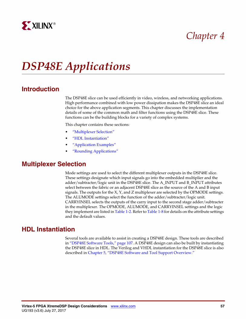
Virtex-5 FPGA XtremeDSP Design Considerations www.xilinx.com 57UG193 (v3.6) July 27, 2017
R
Chapter 4
DSP48E Applications
IntroductionThe DSP48E slice can be used efficiently in video, wireless, and networking applications. High performance combined with low power dissipation makes the DSP48E slice an ideal choice for the above application segments. This chapter discusses the implementation details of some of the common math and filter functions using the DSP48E slice. These functions can be the building blocks for a variety of complex systems.
This chapter contains these sections:
• “Multiplexer Selection”
• “HDL Instantiation”
• “Application Examples”
• “Rounding Applications”
Multiplexer SelectionMode settings are used to select the different multiplexer outputs in the DSP48E slice. These settings designate which input signals go into the embedded multiplier and the adder/subtracter/logic unit in the DSP48E slice. The A_INPUT and B_INPUT attributes select between the fabric or an adjacent DSP48E slice as the source of the A and B input signals. The outputs for the X, Y, and Z multiplexer are selected by the OPMODE settings. The ALUMODE settings select the function of the adder/subtracter/logic unit. CARRYINSEL selects the outputs of the carry input to the second stage adder/subtracter in the multiplexer. The OPMODE, ALUMODE, and CARRYINSEL settings and the logic they implement are listed in Table 1-2. Refer to Table 1-8 for details on the attribute settings and the default values.
HDL InstantiationSeveral tools are available to assist in creating a DSP48E design. These tools are described in “DSP48E Software Tools,” page 107. A DSP48E design can also be built by instantiating the DSP48E slice in HDL. The Verilog and VHDL instantiation for the DSP48E slice is also described in Chapter 5, “DSP48E Software and Tool Support Overview.”

58 www.xilinx.com Virtex-5 FPGA XtremeDSP Design ConsiderationsUG193 (v3.6) July 27, 2017
Chapter 4: DSP48E ApplicationsR
Application Examples
Logic and Bit Field ApplicationThe adder/subtracter/logic unit block in the DSP48E slice can be used to perform bitwise logic operations. The setting of the control bits (OPMODE, CARRYINSEL, and ALUMODE) determine the operation implemented in the DSP48E slice. The operation can be changed dynamically by changing the control bits.
Two 48-Bit Input Bitwise Logic Functions
To implement the two input 48-bit logic functions, the DSP48E slice is configured as a logic unit. This configuration of the DSP48E slice is shown in Figure 4-1.
The functions implemented by the different settings of the ALUMODE bits are shown in Table 1-12.
Dynamic Shifter
A pipelined full-speed 25 x 18 multiply with one of the inputs connected to 2K can shift the other input to the left by K bits. In the process, the output is also shifted right by 18 – K bits. The input value to be shifted, A, can be up to 25 bits wide. However, the shift value, K, can be a maximum of up to 17 bits.
If A is an 18-bit number, a left shift is implemented in the lower 18 bits of the result P[17:0]. These 18 bits represent the A input shifted left by K bits. Similarly, if A is an 18-bit number, the output bits P[35:18] represent the input A shifted right by 18 – K bits and sign-extended.
Figure 4-1: Two-Input 48-Bit Logic Function
UG193_c4_01_091206
A
B
30
A:B 48 P
48
LU18
C
DSP48E_0OPMODE 0110011ALUMODE (As Needed)
0
X
Z

Virtex-5 FPGA XtremeDSP Design Considerations www.xilinx.com 59UG193 (v3.6) July 27, 2017
Application ExamplesR
Dynamic Shifter Example 1
18-bit A input = 11,0011,0011,0011,0011
A sign extended to 25 bits = 1,1111,1111,0011,0011,0011,0011
18-bit B input = 23 or 0….01000
A x B = P = 1111,1111,1111,1111,1111,1111,1111,1001,1001,1001,1001,1000
P[17:0] = 01,1001,1001,1001,1000 = A shifted left by 3
P[35:18] = 11,1111,1111,1111,1110 = A arithmetically shifted right by 15 (note sign extension)
Dynamic Shifter Example 2
18-bit A input = 11,0011,0011,0011,0011
Zero extended to 25 bits = 0,0000,0011,0011,0011,0011,0011
18-bit B input = 23 or 0….01000
A x B = P = 0000,0000,0000,0000,0000,0000,0001,1001,1001,1001,1001,1000
P[17:0] = 01,1001,1001,1001,1000 = A shifted left by 3
P[35:18] = 00,0000,0000,0000,0110 = A logically shifted right by 15
Dynamic Shifter Example 3
“Dynamic Shifter Example 1” and “Dynamic Shifter Example 2” show how the dynamic shifter implemented in a single DSP48E slice can shift an 18-bit number. If A is a 25-bit number, the same technique can also be used to shift A by 0–17 bits.
25-bit A input = 0,1011,0011,0011,0011,0011,0011
18-bit B input = 23 or 0….01000
A x B = P = 0000,0000,0000,0000,0000,0101,1001,1001,1001,1001,1001,1000
P[24:0] = 1,1001,1001,1001,1001,1001,1000 = A shifted left by 3 (Max shift value in one DSP48E is K=17)
P[42:18] = 00,0000,0001,0110,0110 = A shifted right by 15 (Max shift value in one DSP48E is K=17)
Dynamic Shifter Example 4
18-bit A input = 11,0011,0011,0011,0011
A sign extended to 25 bits = 1,1111,1111,0011,0011,0011,0011
18-bit B input = 217 or 10….00000
B is a negative number, but the ALUMODE setting 0011 compensates for this.
A x B = P = 1111,1111,1111,1110,0110,0110,0110,0110,0000,0000,0000,0000
P[17:0] = 10,0000,0000,0000,0000 = A shifted left by 17
P[35:18] = 11,1001,1001,1001,1001 = A arithmetically shifted right by 1
To shift a value by an amount more than 18 bits, two DSP48E slices are used. Figure 4-2 shows the implementation of a dynamic 18-bit shifter. Since the DSP48E slice contains a signed multiplier, the ALUMODE is set to 0011 (subtract) when the MSB of the B input is

60 www.xilinx.com Virtex-5 FPGA XtremeDSP Design ConsiderationsUG193 (v3.6) July 27, 2017
Chapter 4: DSP48E ApplicationsR
a 1. The ALUMODE should have two registers to match the pipeline of the multiplier inputs.
This dynamic shifter is also known as an arithmetic shifter because of the sign extension on the right shift. The behavioral code for the multiplier can be used to implement the dynamic shifter. The multiplier inputs are connected to the value to be shifted and to the shift amount.
Swapping the bit order of the A[24:0] and P[24:0] yields a right-shifted A input without sign extension. In other words, if the shifter input is S[24:0], a right shift of S by K bits without sign-extension can be implemented by connecting S[0:24] to A[24:0]. The shifted output is then S_OUT[0:24] = P[24:0]. This bit swap is not required if the shifter input S[L-1:0] has a size L that is less than 25 bits. In this case, zero-padding the A input MSBs instead of sign extending produces a right shifted value on the output P[L-1:0] with zeros inserted on the left. This is known as logical shift.
18-Bit Barrel Shifter
The barrel shifter function implemented in the DSP48E slice is useful when trying to realign data quickly. Data shifting is required in many operations like address generation and other arithmetic functions. Shifting a single data bit one field at a time is a slow process. Using a barrel shifter, data can be shifted or rotated by any number of bits in a single operation.
Using two DSP48E slices, an 18-bit circular or cyclic barrel shifter can be implemented as shown in Figure 4-3. The barrel shifter shifts the 18-bit value to the left by the amount specified by value K. The bits shifted out of the most-significant part reappear in the lower significant part of the answer, completing the circular shift. The value of 2K is converted to binary using a look up table structure in the block RAM or fabric. The B input and the P output of the first DSP48E slice are connected in cascade to the second DSP48E slice, using BCOUT and PCOUT ports. ALUMODE[1:0] are controlled dynamically by a registered version of the B[17] input to match the internal pipeline stages. The “Barrel Shifter Example” illustrates the barrel shifter application.
Figure 4-2: Dynamic 18-Bit Shift Register
UG193_c4_02_030507
A
2K
Fabric
K B
25
48 P
0
DSP48E_0OPMODE 0000101ALUMODE 0000/0011Sign Extend to A[24]
18±
ALUMODE[1:0]
B[17]

Virtex-5 FPGA XtremeDSP Design Considerations www.xilinx.com 61UG193 (v3.6) July 27, 2017
Application ExamplesR
Barrel Shifter Example
A = 11,0011,0011,0011,0011
Barrel shifting A by 3 (K= 3) generates 01,1001,1001,1001,1110
First DSP48E slice:
A input = 13’b0, A[17:1] = 00,0000,0000,0001,1001,1001,1001,1001
B input = 23 = 1000
Multiplier output (36 bits) = 0000,0000,0000,0000,1100,1100,1100,1100,1000
P output (Adder output) = 0000,0000,0000,0000,0000,0000,0000,1100,1100,1100,1100,1000
P output shifted by 17 from previous slice =0000,0000,0000,0000,0000,0000,0000,0000,0000,0000,0000,0110(17 bits: 0,1100,1100,1100,1000 get truncated)
Second DSP48E slice:
A input = 12’b0, A[17:0] = 00,0000,0000,0011,0011,0011,0011,0011
B input = 23 = 1000
Multiplier output (36 bits) = 0000,0000,0000,0001,1001,1001,1001,1001,1000
P output (adder output) = Multiplier output + cascaded shifted P from previous block= 0000,0000,0000,0000,0000,0000,0001,1001,1001,1001,1001,1110
P[17:0] = 01,1001,1001,1001,1110 = A barrel shifted by 3
Figure 4-3: 18-Bit Barrel Shifter
UG193_c4_03_022607
AA[17:0]
B[17]
0,A[17:1]
18
Shift 17 1
18
A
2KK B
18
0
DSP48E_0OPMODE 0000101ALUMODE 0000/0011
18
DSP48E_1OPMODE 1010101ALUMODE 0000/0011
BCIN
P[17:0]±
±
ALUMODE[1:0]
ALUMODE[1:0]

62 www.xilinx.com Virtex-5 FPGA XtremeDSP Design ConsiderationsUG193 (v3.6) July 27, 2017
Chapter 4: DSP48E ApplicationsR
48-Bit Counter
A counter is one of the most used functions in any digital application. A counter is often used in the control logic. Many times, the counter in a system has to function much faster than the system itself. The DSP48E slice can be used as a high-speed counter, with a performance of over 550 MHz. A counter implemented using the DSP48E slice can achieve high performance with the least amount of resource and power. The DSP48E slice can implement any of theses counters: up counter, down counter, or a loadable counter.
Figure 4-4 shows the implementation of a 48-bit counter using the DSP48E slice. The output is equal to P + C + CARRYIN. For a simple binary counter, CARRYIN is set to 1, and C is set to 0. For a count-by-N counter, the CARRYIN is set to 0, and C is set to N.
The pattern detector can be used to reset the counter without external fabric. This feature, Auto Reset, is described in detail in the “Pattern Detect Applications” section.
Single Instruction Multiple Data (SIMD) Arithmetic
The Viterbi algorithm uses the Add_Compare_Select function, of which the Add and Compare (i.e., subtract) can use the SIMD mode in two separate DSP48E slices. Select must be done in the fabric based on the result of Carryout, sign of input operands, and sign of result. The SIMD mode in the DSP48E slice can be used efficiently to implement a Viterbi algorithm in the Virtex-5 device. This mode can be used to implement the small add-subtract functions at high speed and lower power with less logic utilization.
The adder and subtracter in the adder/subtracted/logic unit can also be split into two 24-bit fields or four 12-bit fields. This is achieved by setting the USE_SIMD attribute. Each of the separate SIMD adders has its own CARRYOUT bit.
When the 48-bit field is split into sets of smaller bit fields, all the different sets perform the same function on the same clock cycle. If one field performs an addition, the other fields can perform only an addition, hence the name “single instruction.” The operation in each field can be dynamically changed from cycle to cycle. The DSP48E slice in SIMD mode is shown in Figure 4-5.
Figure 4-4: 48-Bit Counter
UG193_c4_04_092106
P
0
48C = N
DSP48E_0OPMODE 0001110ALUMODE 0000

Virtex-5 FPGA XtremeDSP Design Considerations www.xilinx.com 63UG193 (v3.6) July 27, 2017
Application ExamplesR
SIMD Absolute Value (24)
Finding the absolute value of a 24-bit or a 12-bit number is another function that can be implemented in the DSP48E slice. A common application for this function is in the motion estimation calculation of a video encoding process. Motion estimation calculates the sum of absolute difference between pixels in adjacent video frames to see which two frames match each other the best. One DSP48E slice can be used in the SIMD mode to find the absolute value, and a second DSP48E slice can be used to calculate the sum of the absolute value. The configuration of the slice is the same as Figure 4-5. The complete implementation is shown in Figure 4-6. To find the absolute value of a 24-bit number, the adder/logic unit is used in the SIMD mode with two 24-bit fields (IN1 = A:B[23:0], C[47:24]. IN2 = A:B[47:24], C[23:0]). One field computes IN1-IN2 and the other field computes IN2-IN1. The output from both of these subtract functions are fed to a multiplexer. The sign bit of one subtract function is used as the multiplexer select. The output of the multiplexer is the absolute value of the 24-bit value. The multiplexer is implemented in the fabric.
The absolute value of two 12-bit numbers can also be determined by using the same process used in the 24-bit number case. The DSP48E slice in the 12-bit case has four outputs. Two separate multiplexers are used in the fabric to get the final two absolute value results.
Figure 4-5: DSP48E Slice in SIMD Mode
UG193_c4_05_022806
A
B
30
A:B 48 P
48
18
C
DSP48E_0OPMODE 0110011ALUMODE (As Needed)Sign Extend Each Small Adder [11,23,35,47]
0
Figure 4-6: Absolute Value Calculation Using DSP48E Slice in SIMD ModeUG193_c4_06_011306
Absolute ValueSEL
Fabric
Sign Bit
IN1 - IN2
IN2 - IN1
DSP Slice inSIMD Mode

64 www.xilinx.com Virtex-5 FPGA XtremeDSP Design ConsiderationsUG193 (v3.6) July 27, 2017
Chapter 4: DSP48E ApplicationsR
Bus Multiplexer
Wide multiplexers are used in many network switching applications where voice and data need to be multiplexed. Video functions, such as scanners, video routers, and pixel-in-pixel switching, require high-speed switching with multiplexers. In digital signal processing, a multiplexer is used to take several separate data streams and combine them into one single data stream at a higher rate. The DSP48E slice can be used to implement high-width (up to 48 bits), multiplexers for networking and video applications.
The OPMODE bits are used to choose between the C input and the A:B input within the DSP48E slice. Each slice can multiplex between two 48-bit values. Figure 4-7 shows the implementation of a 48-bit-wide 8:1 multiplexer. Additional pipeline registers can be used to increase the performance of the multiplexer.
Figure 4-7: 48-Bit-Wide 8:1 Multiplexer Using DSP48E Slices
UG193_c4_07_092206
A
B
30
A:B 48
48
MUX18
C
3
A
B
30
A:B 48
48
MUX18
C
2
A
B
30
A:B 48
48
MUX18
C
1
A
B
30
A:B 48 P
48
MUX18
C
in0
in1
in2
in3
in4
in5
in6
in7
0

Virtex-5 FPGA XtremeDSP Design Considerations www.xilinx.com 65UG193 (v3.6) July 27, 2017
Application ExamplesR
The ALUMODE is set to 0000. Different OPMODE settings can be used for each of the four DSP48E slices. Table 4-1 lists one way of setting the OPMODEs to implement the 48-bit multiplexer.
If the speed of the multiplexer is critical, more pipeline registers can be added. The implementation in Figure 4-7 can be easily extended to perform N:1 multiplexing.
Basic Math Applications
25 x 18 Two's Complement Multiply
A fully pipelined two's complement 25 x 18 multiply is implemented in Figure 4-8. Bypassing the MREG results in reduced speed. If latency is an issue and only one pipeline register can be used, the MREG should always be used.
Sign extension is very important when implementing a multiplier with bit widths less than 25 x 18. When the bit width is less than 25 x 18, the designer must sign-extend the A input all the way up to A[24] and the B input all the way up to B[17]. By setting the sign bits A[24] and B[17] to 0, the DSP48E slice can be used to emulate a 24 x 17 unsigned multiplication. For operands less than 25 x 18, fabric power can be reduced by placing operands into the MSBs and zero padding unused LSBs.
Table 4-1: OPMODE Settings for an 8:1 Multiplexer
OPMODESelected Input
DSP48E_3 DSP48E_2 DSP48E_1 DSP48E_0
xxxxxxx xxxxxxx xxxxxxx 0000011 in 0
xxxxxxx xxxxxxx xxxxxxx 0001100 in 1
xxxxxxx xxxxxxx 0000011 0010000 in 2
xxxxxxx xxxxxxx 0001100 0010000 in 3
xxxxxxx 0000011 0010000 0010000 in 4
xxxxxxx 0001100 0010000 0010000 in 5
0000011 0010000 0010000 0010000 in 6
0001100 0010000 0010000 0010000 in 7
Figure 4-8: Pipelined Two's Complement 25 x 18 Multiplier
UG193_c4_08_092106
A
B
25
48 P
0
DSP48E_0OPMODE 0000101ALUMODE 0000Sign Extend to A[24] and B [17]
18
M

66 www.xilinx.com Virtex-5 FPGA XtremeDSP Design ConsiderationsUG193 (v3.6) July 27, 2017
Chapter 4: DSP48E ApplicationsR
Two Input 48-Bit Addition
The A input in DSP48E slice has been extended to 30 bits. Consequently, the value for A concatenate B is 48 bits. Because the C input is 48-bits wide, C + A:B results in a 48 bit + 48 bit addition, shown in Figure 4-9.
A smaller operand addition in the DSP48E slice (e.g., 38 bits + 38 bits) requires sign extension all the way up to the 48th bit for the C input, namely C[47], and A input, namely A[29].
The addition of two 48-bit numbers can generate a 49th bit. This is the CARRYOUT bit of the DSP48E slice. This CARRYOUT bit allows the adder to be extended beyond 48 bits.
The single CARRYOUT bit is only valid for two input additions. This bit is not valid for three input adds and MACC adds because these additions can generate more than one bit of carry output.
Four Input 46-Bit Addition
Two DSP48E slices can be used to build a four-input 46-bit adder (see Figure 4-10).
Each DSP48E slice adds two 46-bit numbers. The result can be up to 47 bits wide. The 47-bit result from one DSP48E slice is cascaded through the P cascade path into the second DSP48E slice. This 47-bit value is added with the 47-bit result of the second DSP48E slice to give the final 48-bit sum output.
A maximum of 46-bits are used as the input to ensure that there is an adequate number of guard bits to avoid overflow past the available 48 output bits. Sign extension to 48 bits is still required.
The CARRYOUT is not used in this implementation. An external register is used on the C input for pipelining balance.
Figure 4-9: Two Input 48-Bit Addition
UG193_c4_09_022806
A
B
30
A:B 48 P SUM
48
18
C
DSP48E_0OPMODE 0001111ALUMODE 0000Sign Extend to A[29] and C[47]
0

Virtex-5 FPGA XtremeDSP Design Considerations www.xilinx.com 67UG193 (v3.6) July 27, 2017
Application ExamplesR
Two Input 48-Bit Dynamic Add/Subtract
OPMODE settings 0001111 and 0110011 and ALUMODE 0000 implement the A:B + C function. The first OPMODE setting chooses C through the Y multiplexer, and the second OPMODE setting chooses C through the Z multiplexer. OPMODE setting 0001111 consumes slightly lower power than OPMODE 0110011 when performing A:B + C.
The second OPMODE setting 0110011 in conjunction with ALUMODE 0011 allows C – A:B subtract operations to be performed. ALUMODE should be set to 0000 for the add operation and to 0011 for the subtract operation. Figure 4-11 shows the DSP48E implementation of the dynamic add/sub function.
The ALUMODE setting 0001 and CARRYIN = 1 allows A:B – C to be performed. Both ALUMODE and OPMODE can be changed dynamically from cycle to cycle.
The subtraction operation can also be used to detect C > = A:B condition (see Figure 4-37, page 96).
Figure 4-10: Four Input 46-Bit Addition
UG193_c4_10_091806
A
B
30
A:B 48
48
18
C
0
A
B
30
A:B 48
48 48
18
C
1
P SUM
P
DSP48E_1OPMODE 0011111ALUMODE 0000
DSP48E_0OPMODE 0001111ALUMODE 0000Sign Extend to A[29 and C[47]
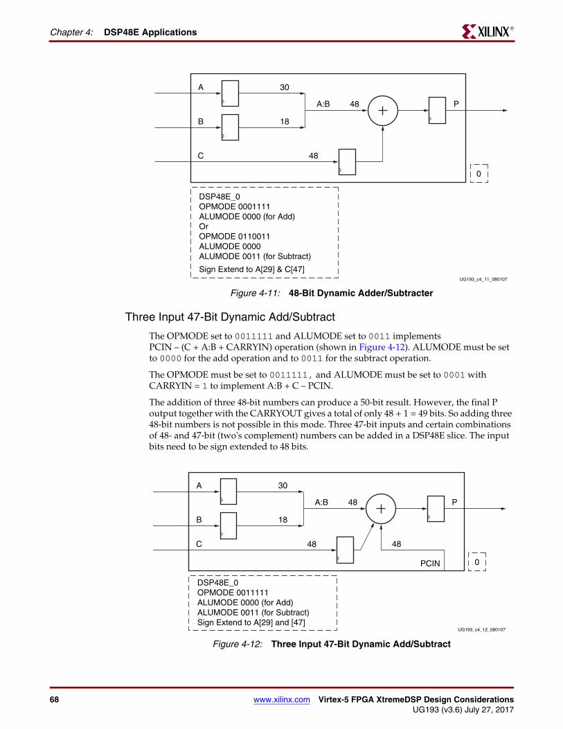
68 www.xilinx.com Virtex-5 FPGA XtremeDSP Design ConsiderationsUG193 (v3.6) July 27, 2017
Chapter 4: DSP48E ApplicationsR
Three Input 47-Bit Dynamic Add/Subtract
The OPMODE set to 0011111 and ALUMODE set to 0011 implements PCIN – (C + A:B + CARRYIN) operation (shown in Figure 4-12). ALUMODE must be set to 0000 for the add operation and to 0011 for the subtract operation.
The OPMODE must be set to 0011111, and ALUMODE must be set to 0001 with CARRYIN = 1 to implement A:B + C – PCIN.
The addition of three 48-bit numbers can produce a 50-bit result. However, the final P output together with the CARRYOUT gives a total of only 48 + 1 = 49 bits. So adding three 48-bit numbers is not possible in this mode. Three 47-bit inputs and certain combinations of 48- and 47-bit (two's complement) numbers can be added in a DSP48E slice. The input bits need to be sign extended to 48 bits.
Figure 4-11: 48-Bit Dynamic Adder/Subtracter
UG193_c4_11_080107
A
B
30
A:B 48 P
48
18
C
DSP48E_0OPMODE 0001111 ALUMODE 0000 (for Add)OrOPMODE 0110011ALUMODE 0000 ALUMODE 0011 (for Subtract)
0
Sign Extend to A[29] & C[47]
Figure 4-12: Three Input 47-Bit Dynamic Add/Subtract
UG193_c4_12_080107
A
B
30
A:B 48 P
PCIN
48
18
C
DSP48E_0OPMODE 0011111ALUMODE 0000 (for Add)ALUMODE 0011 (for Subtract)Sign Extend to A[29] and [47]
0
48

Virtex-5 FPGA XtremeDSP Design Considerations www.xilinx.com 69UG193 (v3.6) July 27, 2017
Application ExamplesR
25 x 18 Multiply Plus 48-Bit Add/Sub
The DSP48E slice can be used to implement a multiply-add or a multiply-subtract operation (see Figure 4-13). The largest multiplication that can be done using one slice is a 25 x 18 bit multiplication. The output of the multiplier is then added or subtracted from the 48-bit C input value.
Setting the OPMODE to 0110101 and the ALUMODE to 0000 implements an adder:
Equation 4-1
Setting OPMODE to 0110101 and ALUMODE to 0011 implements:
Equation 4-2
Because the A and B inputs are registered twice (AREG/BREG and MREG), two registers should be used on the C input. One of the C input registers should be implemented in the fabric, external to the DSP48E slice.
Figure 4-13: Multiply Add and Multiply Sub Functions
P C A( B )×+=
P C A( B )×–=
UG193_c4_13_092106
A
B
25
P
0
DSP48E_0OPMODE 0110101ALUMODE 0000 (for Add)ALUMODE 0011 (for Subtract)Sign Extend to A[24], B[17], and C[47]
18
48C

70 www.xilinx.com Virtex-5 FPGA XtremeDSP Design ConsiderationsUG193 (v3.6) July 27, 2017
Chapter 4: DSP48E ApplicationsR
Extended Multiply
The 25 x 18 multiply can be extended to a 26 x 18 or 25 x 19 multiply if needed. The extended multiply function uses one DSP48E slice output concatenated with a one-bit AND function output in the fabric. This implementation is expressed in Equation 4-3, and the equation can be implemented as shown in Figure 4-14.
Equation 4-3
The largest multiplier that can be implemented in two DSP48E slices is a 35 x 25 multiplier. For the 35 x 25 bit multiplier, the A input of the first DSP48E slice is connected to A[24:0], and the B input is connected to {0,B[16:0]}. The A input of the second DSP48E slice is connected to A[24:0] through the cascaded path. The B input is connected to {0,B[34:17]}. The output of the first DSP48E slice is connected to the adder of the second DSP48E slice through the 17-bit shift PCIN path. The first DSP48E slice produces the 17 LSBs of the final product. Bits [59:17] of the final product are obtained at the output of the second DSP48E slice. Larger multipliers can be implemented using a single DSP48E slice taking multiple cycles, or they can be implemented in multiple slices taking a single cycle. See Table 4-2.
A[25:0] B[17:0]{( A[25:1] B[17:0]×( )
=×A[0] AND B[17:1]( )), A( [0] AND B[0] )}+
Figure 4-14: Multiplication Extension by One Bit
UG193_c4_14_092106
AA[25:1]
B[17:0]
Reset This ExternalRegister
if A[0] is Low
Signext, B[17:1]
B
B[0]
A[0]
25
43
48
OUT[44:1]
0
DSP48E_0OPMODE 0110101ALUMODE 0000Sign Extend to C[47]
18
Fabric
48C
OUT[0]
P[43:0]

Virtex-5 FPGA XtremeDSP Design Considerations www.xilinx.com 71UG193 (v3.6) July 27, 2017
Application ExamplesR
Floating Point Multiply and 59 x 59 Signed Multiply
Single precision floating point multipliers require an unsigned 24 x 24 multiply that can be implemented with a 35 x 25 signed multiplier, described in Table 4-2, by setting the extra sign bits to 0. Double precision floating point multipliers require a 53 x 53 unsigned multiply that can be implemented in the 59 x 59 signed multiplier demonstrated in Figure 4-15 and Figure 4-16—again by setting the extra sign bits to 0. Figure 4-15 and Figure 4-16 conceptually illustrate how a 59 x 59 signed multiply (R[58:0] x S[58:0]) can be implemented using 10 DSP48E slices.
Additional features related to the IEEE Floating Point standard must be implemented in fabric. Floating point cores are also available from the CORE Generator™ tool.
Table 4-2: Utilization and Latency Table for Different Sized Multipliers
Multiply SizeNumber of
DSP48E Slices
Latency Notes
A[24:0] x B[17:0] 1 3 DSP1 = 25 x 18
A[24:0] x B[34:0] 2 4 DSP1 = (A[24:0] x (0, B[16:0]))
DSP2 = (A[24:0] x B[34:17]) + PCIN shift17 of DSP1
A[41:0] x B[34:0] 4 6 DSP1 = (0, A[16:0]) x (0, B[16:0])
DSP2 = (A[41:17] x (0, B[16:0])) + PCIN shift17 of DSP1
DSP3 = ((0, A[16:0]) x B[4:17]) + PCIN of DSP2
DSP4 = (A[41:17] x B[35:17]) + PCIN shift17 of DSP3

72 www.xilinx.com Virtex-5 FPGA XtremeDSP Design ConsiderationsUG193 (v3.6) July 27, 2017
Chapter 4: DSP48E ApplicationsR
Figure 4-15: 59 x 59: Lower Five DSP48E Slices
UG193_c4_41_030507
A8’b0, R[33:17]
8’b0, R[16:0]
25
Shift 17 1
18
A
B
25
0
18
BCIN
A 25
2
18B
A 25
Shift 17 3
18
BCIN
A 25
4
18B
0, S[16:0]
P[16:0] PROD[16:0]Z-9
P[16:0] PROD[33:17]Z-7
PCOUT4[47:0]
OPMODE 0000101
OPMODE 1010101
OPMODE 0010101
OPMODE 1010101
OPMODE 0010101
8’b0, R1[16:0]
0, S1[33:17]
8’b0, R2[33:17]
R3[58:34]
0, S3[16:0]
8’b0, R[16:0]
0, S[33:17]
8’b0, R[33:17]
0, S[16:0]
Z-3
Z-3
Z-2
R[58:34]SRL16
SRL16
SRL16
SRL16
SRL16

Virtex-5 FPGA XtremeDSP Design Considerations www.xilinx.com 73UG193 (v3.6) July 27, 2017
Application ExamplesR
Figure 4-16: 59 x 59: Upper Five DSP48E Slices
UG193_c4_42_030608
Shift 17ACIN
A 25
6
18B
OPMODE 1010101
Z-5
A 25
18B
PCOUT4[47:0]
OPMODE 0010101
S4[58:34]
0, R4[16:0]
0, R5[33:17]
0, R[16:0]
0, R[33:17]
0, S[33:17]
0, S[50:34]
Sign Extend, S[58:51]
Z-4
Z-4
S[58:34]
5
P[16:0] PROD[50:34]Z-4
Shift 17ACIN
A 25
8
18B
OPMODE 1010101
Z-7
A 25
18B
OPMODE 0010101
R6[58:34]
0, S6[33:17]
0, S7[50:34]
Z-6
Z-6
R[58:34]
7
P[16:0] PROD[67:51]Z-2
Shift 17ACIN
A 25
9
18B
OPMODE 1010101
Sign Extend, S8[58:51]Z-8
P[16:0] PROD[84:68]
P[32:0] = PROD[117:85]
SRL16
SRL16
SRL16
SRL16
SRL16
SRL16
SRL16
SRL16
SRL16
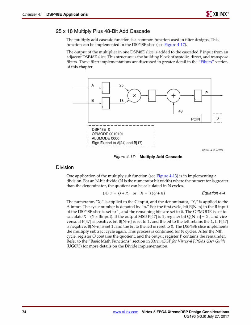
74 www.xilinx.com Virtex-5 FPGA XtremeDSP Design ConsiderationsUG193 (v3.6) July 27, 2017
Chapter 4: DSP48E ApplicationsR
25 x 18 Multiply Plus 48-Bit Add Cascade
The multiply add cascade function is a common function used in filter designs. This function can be implemented in the DSP48E slice (see Figure 4-17).
The output of the multiplier in one DSP48E slice is added to the cascaded P input from an adjacent DSP48E slice. This structure is the building block of systolic, direct, and transpose filters. These filter implementations are discussed in greater detail in the “Filters” section of this chapter.
Division
One application of the multiply sub function (see Figure 4-13) is in implementing a division. For an N-bit divide (N is the numerator bit width) where the numerator is greater than the denominator, the quotient can be calculated in N cycles.
Equation 4-4
The numerator, “X,” is applied to the C input, and the denominator, “Y,” is applied to the A input. The cycle number is denoted by “n.” For the first cycle, bit B[N–n] in the B input of the DSP48E slice is set to 1, and the remaining bits are set to 0. The OPMODE is set to calculate X – (Y x Binput). If the output MSB P[47] is 1, register bit Q[N–n] = 0, and vice-versa. If P[47] is positive, bit B[N–n] is set to 1, and the bit to the left retains the 1. If P[47] is negative, B[N–n] is set 1, and the bit to the left is reset to 0. The DSP48E slice implements the multiply subtract cycle again. This process is continued for N cycles. After the Nth cycle, register Q contains the quotient, and the output register P contains the remainder. Refer to the “Basic Math Functions” section in XtremeDSP for Virtex-4 FPGAs User Guide (UG073) for more details on the Divide implementation.
Figure 4-17: Multiply Add Cascade
UG193_c4_15_022806
A
B
25
P
0
DSP48E_0OPMODE 0010101ALUMODE 0000Sign Extend to A[24] and B[17]
18
PCIN
48
X Y Q R+=⁄( ) or X Y Q R+( )=

Virtex-5 FPGA XtremeDSP Design Considerations www.xilinx.com 75UG193 (v3.6) July 27, 2017
Application ExamplesR
Advanced Math Applications
Accumulate
The operands in an accumulate function can extend up to 48 bits. A 48-bit operand could cause overflow during the accumulate operation. To prevent this overflow, it is best to use an operand width that is much less than 48 bits wide. An operand that is much less than 48 bits wide (e.g., N-bit-wide) could still cause an overflow after 2 (48-N) accumulate cycles. Overflowing past the MSB (48th) sign bit could invalidate the accumulate function.
Larger accumulators can be implemented by extending the accumulate operation to a second DSP48E slice. This is done using the cascadeable carry output CARRYCASCOUT bit. The CARRYOUT bit can also be taken out to the fabric and can be used to extend the accumulate function in the fabric. Figure 4-18 shows the implementations of a 48-bit accumulate function.
Two Input 48-Bit Add Accumulate
The three-input adder can be configured as a two-input adder plus an accumulator (see Figure 4-19). This implementation can effectively act as a one-input accumulator that is running at 2X the speed because two inputs can be added to the accumulated value on each 550 MHz clock cycle.
Sufficient guard bits should be left in this implementation to avoid the chance of overflow. This is described in Figure 4-19. Because a three-input add produces two carry out bits, the single CARRYOUT bit of a 48-bit operation (Carryout[3]) is insufficient to extend three-input adds.
Figure 4-18: 48-Bit Accumulate Function
UG193_c4_16_022806
P
0
4848 48C
DSP48E_0OPMODE 0001110ALUMODE 0000Sign Extend to C[47]

76 www.xilinx.com Virtex-5 FPGA XtremeDSP Design ConsiderationsUG193 (v3.6) July 27, 2017
Chapter 4: DSP48E ApplicationsR
Dynamic Add/Sub Accumulate
Certain types of subtractions can be accumulated using the DSP48E slice. Setting the OPMODE bits to 0101111 and the ALUMODE mode bits to 0011 implements:
Equation 4-5
The addition and subtraction can be dynamically changed by toggling the ALUMODE bits between 0000 and 0011.
The 48-bit dynamic add/sub accumulator is shown in Figure 4-20.
Figure 4-19: Two 48-Bit Add Accumulate Function
UG193_c4_17_022806
A
B
30
A:B 48 P
4848 48
18
C
DSP48E_0OPMODE 0101111ALUMODE 0000Sign Extend to A[29] and C[47]
0
Figure 4-20: 48-Bit Dynamic Add/Sub Accumulator
P P A:B + C + Carryin( )–=
UG193_c4_18_092206
A
B
30
A:B 48 P
4848 48
18
C
DSP48E_0OPMODE 0101111ALUMODE 0000 (for Add)ALUMODE 0011 (for Subtract)Sign Extend to A[29] and C[47]
0
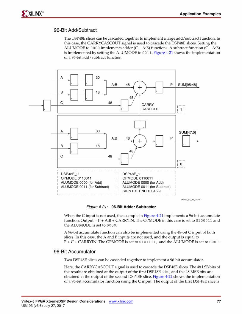
Virtex-5 FPGA XtremeDSP Design Considerations www.xilinx.com 77UG193 (v3.6) July 27, 2017
Application ExamplesR
96-Bit Add/Subtract
The DSP48E slices can be cascaded together to implement a large add/subtract function. In this case, the CARRYCASCOUT signal is used to cascade the DSP48E slices. Setting the ALUMODE to 0000 implements adder (C + A:B) functions. A subtract function (C – A:B) is implemented by setting the ALUMODE to 0011. Figure 4-21 shows the implementation of a 96-bit add/subtract function.
When the C input is not used, the example in Figure 4-21 implements a 96-bit accumulate function: Output = P + A:B + CARRYIN. The OPMODE in this case is set to 0100011 and the ALUMODE is set to 0000.
A 96-bit accumulate function can also be implemented using the 48-bit C input of both slices. In this case, the A and B inputs are not used, and the output is equal to P + C + CARRYIN. The OPMODE is set to 0101111, and the ALUMODE is set to 0000.
96-Bit Accumulator
Two DSP48E slices can be cascaded together to implement a 96-bit accumulator.
Here, the CARRYCASCOUT signal is used to cascade the DSP48E slices. The 48 LSB bits of the result are obtained at the output of the first DSP48E slice, and the 48 MSB bits are obtained at the output of the second DSP48E slice. Figure 4-22 shows the implementation of a 96-bit accumulator function using the C input. The output of the first DSP48E slice is
Figure 4-21: 96-Bit Adder Subtracter
UG193_c4_20_072407
A
B
30
A:B 48 P
4848
18
C
DSP48E_0OPMODE 0110011ALUMODE 0000 (for Add)ALUMODE 0011 (for Subtract)
DSP48E_1OPMODE 0110011ALUMODE 0000 (for Add)ALUMODE 0011 (for Subtract)SIGN EXTEND TO A[29]
0
A
B
30
A:B 48
4848
18
C
P SUM[95:48]
SUM[47:0]
CARRYCASCOUT 1

78 www.xilinx.com Virtex-5 FPGA XtremeDSP Design ConsiderationsUG193 (v3.6) July 27, 2017
Chapter 4: DSP48E ApplicationsR
equal to P + C. The OPMODE in this case is set to 0101100, and the ALUMODE is set to 0000. The output of the second DSP48E slice is equal to P + A:B. The OPMODE in this case is set to 0100011, and the ALUMODE is set to 0000.
Instead of the C input, the A:B input with one pipeline register can also be used to implement the output in the first DSP48E slice. The second DSP48E slice should, however, use the A:B input with two pipeline registers for alignment with the CARRYCASCOUT signal.
MACC and MACC Extension
A pipelined full speed 25 x 18 multiply followed by an accumulate (MACC) operation is shown in Figure 4-23. The OPMODEREG and the CARRYINSELREG must both be set to 1 on both the upper and lower DSP48E slices.
A 25 x 18 multiply yields 43 bits, and unlike the Virtex-4 device, the DSP48E slice is more likely to overflow during MACC operations. One solution is to use the “overflow” signals to detect overflow past P[46] or to use the pattern detector directly to detect overflow past P[47]. This is described in the “Overflow/Underflow/Saturation Past P[47]” section.
Another option is to use a second DSP48E slice (see Figure 4-23) and some external muxes and flip-flops. The special OPMODE 1001000 in the second DSP48E slice adds together P and MULTSIGNOUT from the previous DSP48E slice. CARRYINSEL must also be set to 010 in order to add in CARRYCASCOUT. This special OPMODE setting, therefore, extends a MACC operation from a lower DSP48E slice. This special MACC extend mode can only be selected after a reset. Thus each time the accumulator is reset, the OPMODE on
Figure 4-22: 96-Bit Accumulator
UG193_c4_21_072407
P
4848
C
DSP48E_0OPMODE 0101100ALUMODE 0000 (for Add)ALUMODE 0011 (for Subtract)
DSP48E_1OPMODE 0100011ALUMODE 0000 (for Add)ALUMODE 0011 (for Subtract)SIGN EXTEND TO A[29]
0
A
B
A:B 48
4818
P SUM[95:48]
SUM[47:0]
CARRYCASCOUT 1
48
30
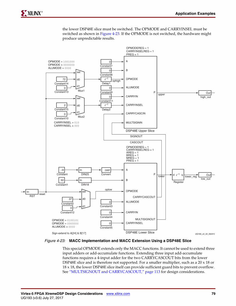
Virtex-5 FPGA XtremeDSP Design Considerations www.xilinx.com 79UG193 (v3.6) July 27, 2017
Application ExamplesR
the lower DSP48E slice must be switched. The OPMODE and CARRYINSEL must be switched as shown in Figure 4-23. If the OPMODE is not switched, the hardware might produce unpredictable results.
This special OPMODE extends only the MACC functions. It cannot be used to extend three input adders or add-accumulate functions. Extending three input add-accumulate functions requires a 4-input adder for the two CARRYCASCOUT bits from the lower DSP48E slice and is therefore not supported. For a smaller multiplier, such as a 20 x 18 or 18 x 18, the lower DSP48E slice itself can provide sufficient guard bits to prevent overflow. See “MULTSIGNOUT and CARRYCASCOUT,” page 113 for design considerations.
Figure 4-23: MACC Implementation and MACC Extension Using a DSP48E Slice
DSP48E Upper Slice
DSP48E Lower Slice
Register
Convert
RST
DIN25
DIN18
Constant
Constant1
reset
low_out
high_out
lower_reg
upper
SIGNOUT
CASCOUT
lower Out
OPMODEREG = 1CARRYINSELREG = 1AREG = 1BREG = 1MREG = 1PREG = 1
OPMODEREG = 1CARRYINSELREG = 1PREG = 1
OPMODE = 1001000OPMODE = 0000000ALUMODE = 0000
OPMODE = 0100101OPMODE = 0000000ALUMODE = 0000
Sign-extend to A[24] & B[17]
CARRYINSEL = 010CARRYINSEL = 000
ALUMODE
OPMODEoplowsel
d0
d1
sel
d0
d1
sel
d0
d1
B
A
MULTSIGNIN
CARRYCASCIN
CARRYINSEL
CARRYIN
ALUMODE
OPMODE
Constant7
Constant3Constant2
Constant4
Constant5
Constant8
Constant9
Constant11
Constant14
Constant15
Constant13
Constant10
Constant12
Delay1ophigh
Mux1
Mux2
Delay2
B
A
CARRYIN
CARRYINSELMULTISIGNOUT
CARRYCASCOUT
P
72
0
0
0
0
0
2
0
37
0
0
0
0
–9 castIn
In
In
50
Out
d qz–1
z–1
z–1
P
UG193_c4_22_052410

80 www.xilinx.com Virtex-5 FPGA XtremeDSP Design ConsiderationsUG193 (v3.6) July 27, 2017
Chapter 4: DSP48E ApplicationsR
25 x 18 Complex Multiply
A 25 x 18 complex multiply function is implemented using the DSP48E slices in Figure 4-24. A complex multiply function is:
Equation 4-6
Two DSP48E slices implement the real part and two slices are used to implement the imaginary part. The real and imaginary results use the same slice configuration with the exception of the adder/subtracter. The A and B input register pipe stages are matched between the slices for the real and imaginary parts. A similar technique can be used to implement a butterfly computation in the FFT algorithm.
A ja+( ) B( jb ) A( B ab )– j A( b Ba )+×=+×
Figure 4-24: 25 x 18 Complex Multiply
UG193_c4_23_051010
B[17:0]
A[24:0]
A
B
P
2
25
18
A
B
P
a[24:0]
b[17:0]
A[24:0]
b[17:0]
1
25
18
A
B
P
a[24:0]
B[17:0]
3
IMAGINARY_OUT[43:0]
REAL_OUT[43:0]
25
18
A
B
P
0
DSP48E_0OPMODE 0000101ALUMODE 0000
DSP48E_1OPMODE 0010101ALUMODE 0011
DSP48E_2OPMODE 0000101ALUMODE 0000
DSP48E_3OPMODE 0010101ALUMODE 0000
25
18

Virtex-5 FPGA XtremeDSP Design Considerations www.xilinx.com 81UG193 (v3.6) July 27, 2017
Application ExamplesR
35 x 25 Complex Multiply
Many complex multiply algorithms require higher precision in one of the operands. The equations for combining the real and imaginary parts in complex multiplication are the same, but the larger operands must be separated into two parts and combined using partial product techniques. The real and imaginary results use the same slice configuration with the exception of the adder/subtracter. The adder/subtracter performs subtraction for the real result and addition for the imaginary result. Equation 4-7 and Equation 4-8 describe the math used to form the real and imaginary parts for the fully pipelined, complex, 35-bit x 25-bit multiplication.
Equation 4-7
Equation 4-8
Figure 4-25 shows the real part of a fully pipelined, complex, 35 x 25 multiplier.
A[24:0] ja[24:0] )+ B( [34:0] jb[34:0] )+×(
REAL_OUT A( [24:0] B[34:17] ) SHIFT17 A[24:0] 0( B[16:0] ),×{ }a( [24:0] b[34:17]×
–+×) SHIFT17 a[24:0]{ 0 b[16:0] ) },(×–
=
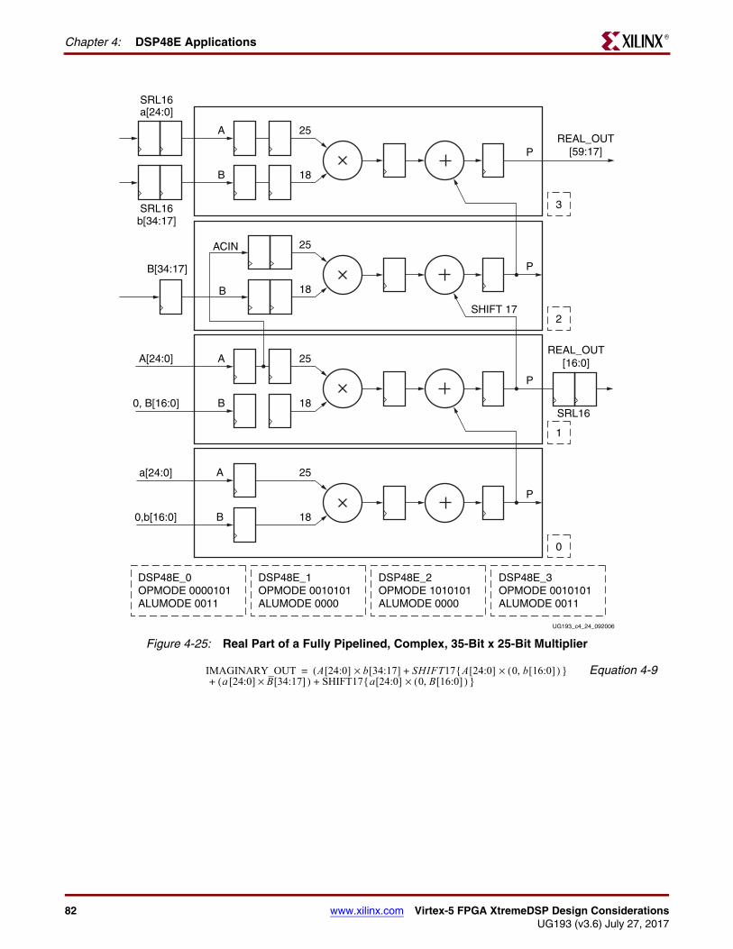
82 www.xilinx.com Virtex-5 FPGA XtremeDSP Design ConsiderationsUG193 (v3.6) July 27, 2017
Chapter 4: DSP48E ApplicationsR
Equation 4-9
Figure 4-25: Real Part of a Fully Pipelined, Complex, 35-Bit x 25-Bit Multiplier
UG193_c4_24_092006
0,b[16:0]
a[24:0]
B
ACIN
P
2
25
18
A
B
P
A[24:0]
0, B[16:0]
B[34:17]
1
25
18
A
B
P
SHIFT 17
a[24:0]
b[34:17]
3
REAL_OUT[59:17]
REAL_OUT[16:0]
25
18
A
B
P
0
DSP48E_0OPMODE 0000101ALUMODE 0011
DSP48E_1OPMODE 0010101ALUMODE 0000
DSP48E_2OPMODE 1010101ALUMODE 0000
DSP48E_3OPMODE 0010101ALUMODE 0011
25
18
SRL16
SRL16
SRL16
IMAGINARY_OUT A[24:0]( b[34:17] SHIFT17 A[24:0]{ 0 b[16:0] ) },(×+×a( [24:0] B[34:17] )× SHIFT17 a[24:0]{ 0 B[16:0] ) },(×+ +
=
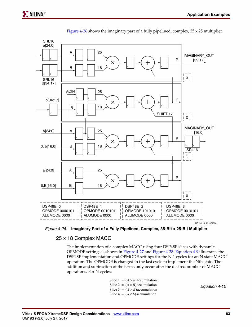
Virtex-5 FPGA XtremeDSP Design Considerations www.xilinx.com 83UG193 (v3.6) July 27, 2017
Application ExamplesR
Figure 4-26 shows the imaginary part of a fully pipelined, complex, 35 x 25 multiplier.
25 x 18 Complex MACC
The implementation of a complex MACC using four DSP48E slices with dynamic OPMODE settings is shown in Figure 4-27 and Figure 4-28. Equation 4-9 illustrates the DSP48E implementation and OPMODE settings for the N-1 cycles for an N state MACC operation. The OPMODE is changed in the last cycle to implement the Nth state. The addition and subtraction of the terms only occur after the desired number of MACC operations. For N cycles:
Equation 4-10
Figure 4-26: Imaginary Part of a Fully Pipelined, Complex, 35-Bit x 25-Bit Multiplier
UG193_c4_25_071006
0,B[16:0]
a[24:0]
B
ACIN
P
2
25
18
A
B
P
A[24:0]
0, b[16:0]
b[34:17]
1
25
18
A
B
P
SHIFT 17
B[34:17]3
25
18
A
B
P
0
DSP48E_0OPMODE 0000101ALUMODE 0000
DSP48E_1OPMODE 0010101ALUMODE 0000
DSP48E_2OPMODE 1010101ALUMODE 0000
DSP48E_3OPMODE 0010101ALUMODE 0000
25
18
IMAGINARY_OUT[59:17]
IMAGINARY_OUT[16:0]
a[24:0]SRL16
SRL16
SRL16
Slice 2 a B×( )accumulation=Slice 3 A B×( )accumulation=Slice 4 a b×( )accumulation=
Slice 1 A b×( )accumulation=
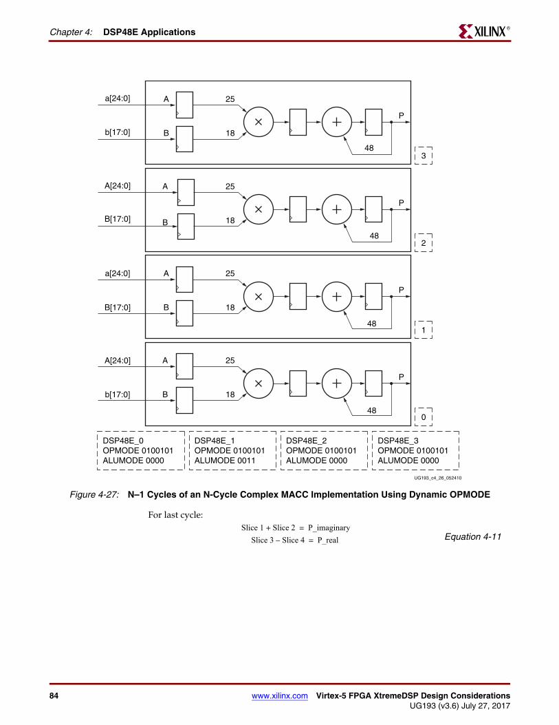
84 www.xilinx.com Virtex-5 FPGA XtremeDSP Design ConsiderationsUG193 (v3.6) July 27, 2017
Chapter 4: DSP48E ApplicationsR
For last cycle:
Equation 4-11
Figure 4-27: N–1 Cycles of an N-Cycle Complex MACC Implementation Using Dynamic OPMODE
UG193_c4_26_052410
b[17:0]
A[24:0]
A
B
P
2
25
18
A
B
P
48
a[24:0]
B[17:0]
B[17:0]
A[24:0]
1
48
25
18
A
B
P
48
48
a[24:0]
b[17:0]
3
25
18
A
B
P
0
DSP48E_0OPMODE 0100101ALUMODE 0000
DSP48E_1OPMODE 0100101ALUMODE 0011
DSP48E_2OPMODE 0100101ALUMODE 0000
DSP48E_3OPMODE 0100101ALUMODE 0000
25
18
Slice 1 Slice 2+ P_imaginary=
Slice 3 Slice 4– P_real=

Virtex-5 FPGA XtremeDSP Design Considerations www.xilinx.com 85UG193 (v3.6) July 27, 2017
Application ExamplesR
During the last cycle, the input data must stall while the final terms are added. To avoid having to stall the data, the complex multiply implementation, shown in Figure 4-29, should be used (instead of using the complex multiply implementation shown in Figure 4-27 and Figure 4-28).
Figure 4-28: Nth Cycle of an N-Cycle Complex MACC Implementation Using Dynamic OPMODE
UG193_c4_27_022806
DSP48E_0OPMODE 0000000ALUMODE 0000
DSP48E_1OPMODE 0011110ALUMODE 0000
DSP48E_2OPMODE 0000000ALUMODE 0000
DSP48E_3OPMODE 0011110ALUMODE 0000
48 48
P
48CRound
3
P
2
48 48
PREAL_OUT
[47:0]
48CRound
1
P
0
IMAGINARY_OUT[47:0]

86 www.xilinx.com Virtex-5 FPGA XtremeDSP Design ConsiderationsUG193 (v3.6) July 27, 2017
Chapter 4: DSP48E ApplicationsR
Figure 4-29: Complex MACC Implementation
48 48
P
48CRound
IMAGINARY_OUT[47:0]
REAL_OUT[47:0]
5
A
B
P
a[24:0]
B[17:0]
4
25
18
b[17:0]
A[24:0] A
B
P
3
25
18
48 48
P
48CRound
2
A
B
P
a[24:0]
b[17:0]
1
25
18
B[17:0]
A[24:0] A
B
P
0
25
18
UG193_c4_28_020508
DSP48E_0OPMODE 0000101ALUMODE 0000
DSP48E_1OPMODE 0010101ALUMODE 0011
DSP48E_2OPMODE 0011110ALUMODE 0000
DSP48E_3OPMODE 0000101ALUMODE 0000
DSP48E_4OPMODE 0010101ALUMODE 0000
DSP48E_5OPMODE 0011110ALUMODE 0000
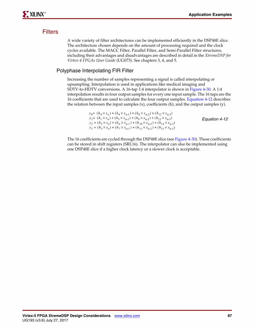
Virtex-5 FPGA XtremeDSP Design Considerations www.xilinx.com 87UG193 (v3.6) July 27, 2017
Application ExamplesR
FiltersA wide variety of filter architectures can be implemented efficiently in the DSP48E slice. The architecture chosen depends on the amount of processing required and the clock cycles available. The MACC Filter, Parallel Filter, and Semi-Parallel Filter structures, including their advantages and disadvantages are described in detail in the XtremeDSP for Virtex-4 FPGAs User Guide (UG073). See chapters 3, 4, and 5.
Polyphase Interpolating FIR Filter
Increasing the number of samples representing a signal is called interpolating or upsampling. Interpolation is used in applications like medical imaging and SDTV-to-HDTV conversions. A 16-tap 1:4 interpolator is shown in Figure 4-30. A 1:4 interpolation results in four output samples for every one input sample. The 16 taps are the 16 coefficients that are used to calculate the four output samples. Equation 4-12 describes the relation between the input samples (x), coefficients (h), and the output samples (y).
Equation 4-12
The 16 coefficients are cycled through the DSP48E slice (see Figure 4-30). These coefficients can be stored in shift registers (SRL16). The interpolator can also be implemented using one DSP48E slice if a higher clock latency or a slower clock is acceptable.
y0 h( 0 xn× ) h4 xn-1×( ) h8 xn-2×( ) h12 xn-3×( )y1 h1 xn×( ) h5 xn-1×( ) h9 xn-2×( ) h13 xn-3×( )y2 h2 xn×( ) h( 6 xn-1 ) h( 10 xn-2 ) h14 xn-3×( )+×+×y3 h3 xn×( )= h( 7 xn-1 ) h( 11 xn-2 ) h15 xn-3×( )+×+×
++
=+ + +=+ + +=

88 www.xilinx.com Virtex-5 FPGA XtremeDSP Design ConsiderationsUG193 (v3.6) July 27, 2017
Chapter 4: DSP48E ApplicationsR
Included in the reference design files for this chapter is PolyIntrpFilter.zip, which provides examples of portable, parameterized, design, and simulation VHDL files that infer DSP48E slices when creating Polyphase Interpolating FIR filters in Virtex®-5 devices. The number of filter taps, interpolation factors, and data bit widths are parameterizable. Synplify 8.1 was used to synthesize this portable, RTL VHDL code with generics for parameterization. The reference design files associated with this user guide can be found on the Virtex-5 FPGA page on xilinx.com.
Polyphase Decimating FIR Filter
Decimating is the process of reducing the number of samples representing a signal. Decimation is used in video applications like 4:4:4-to-4:2:2 conversions and HDTV-to-SDTV conversions. Figure 4-31 shows a 16-tap 4:1 decimator implemented using four parallel filters. For every four input sample, the decimator produces one output sample.
Figure 4-30: 16-Tap 1:4 Interpolator
B
y[-4]43SRL16h(14)h(15)h(12)h(13) 3
25
18
ACIN
ACIN
ACIN
B
P
2
25
18
B
P
1
25
18
A
B
P
0
25
18
UG193_c4_29_092206
DSP48E_1OPMODE 0010101ALUMODE 0000
DSP48E_2OPMODE 0010101ALUMODE 0000
DSP48E_3OPMODE 0010101ALUMODE 0000
DSP48E_0OPMODE 0000101ALUMODE 0000
SRL16h(11)h(8)h(9)h(10)
SRL16h(4)h(5)h(6)h(7)
SRL16h(3)h(2)h(1)h(0)
x[n+2]
43
43
43

Virtex-5 FPGA XtremeDSP Design Considerations www.xilinx.com 89UG193 (v3.6) July 27, 2017
Application ExamplesR
For the 16-tap filter, the output sample (y) is the weighted average of 16 input samples (x) multiplied by 16 coefficients (h) as described in Equation 4-13.
Equation 4-13
The input signals to each DSP48E slice are delayed by (M+1) clocks from the previous slice. Shift registers are used to achieve this delay. After an initial latency, the four tap filter output is obtained at the fourth DSP48E slice. This output is accumulated with the previous values in the final DSP48E slice. This final slice is in the accumulation mode for
y0 h0 xn×( ) h1 xn-1×( ) h2 xn-2×( ) h3 xn-3×( ) h4 xn-4×( )h5 xn-5×( ) h6 xn-6×( ) h7 xn-7×( ) h8 xn-8×( ) h9 xn-9×( ) h10 xn-10×( )h11 xn-11×( ) h12 xn-12×( ) h13 xn-13×( ) h14 xn-14×( ) h15 xn-15×( )
+ + + + ++ + + + +
+ + + + +
=
Figure 4-31: 16-Tap 1:4 Decimator
B
43
43
43
43
SRL16h(14)h(13)h(12)h(15)
M+1FIFO
M+1FIFO
M+1FIFO
25
18
B
P
25
18
B
P
25
18
A
A
A
A
B
P
25
18
UG193_c4_30_032806
DSP48E_1OPMODE 0010101ALUMODE 0000
DSP48E_2OPMODE 0010101ALUMODE 0000
DSP48E_3OPMODE 0010101ALUMODE 0000
DSP48E_4OPMODE 0010101ALUMODE 0000
DSP48E_0OPMODE 0000101ALUMODE 0000
ce 1/m
P
48
SRL16h(9)h(8)h(11)h(10)
SRL16h(4)h(7)h(6)h(5)
SRL16h(3)h(2)h(1)h(0)
M+1FIFO
x[n+1]
y[-2]
0
1
2
3
4

90 www.xilinx.com Virtex-5 FPGA XtremeDSP Design ConsiderationsUG193 (v3.6) July 27, 2017
Chapter 4: DSP48E ApplicationsR
four cycles. This filter structure (see Figure 4-31) can also be used as a folded single-rate 16-tap filter.
Included in the reference design files for this chapter is PolyDecFilter.zip,which provides examples of portable, parameterized, design, and simulation VHDL files that infer DSP48E slices when creating Polyphase Decimating FIR filters in Virtex-5 devices. The number of filter taps, decimation factors, and data bit widths are parameterizable. Synplify 8.1 was used to synthesize this portable, RTL VHDL code with generics for parameterization. The reference design files associated with this user guide can be found on the Virtex-5 FPGA page on xilinx.com.
Multichannel FIR
Multichannel filtering is used in applications like wireless communication, image processing, and multimedia applications. In a typical multichannel filtering scenario, multiple input channels are filtered using a separate digital filter for each channel. Due to the high performance of the DSP48E slice, time division multiplexing can be used to filter up to N separate channels using one DSP48E slice. The number of channels N is calculated by:
N x channel frequency ≤ maximum frequency of the DSP48E slice
Each DSP48E slice is clocked using an NX clock. The N input streams are converted to one parallel, interleaved stream using the N to one multiplexer. The multiplexer is designed so that the maximum delay is equal to one LUT delay. This ensures the best performance. The N parallel interleaved streams are stored in an N+1 FIFO. This implementation uses 1/Nth of the total FPGA resource as compared to implementing each channel separately. Figure 4-32 shows a four-tap, four-channel filter implementation. Refer to the XtremeDSP for Virtex-4 FPGAs User Guide, Chapter 6, for a detailed multichannel filter application note.

Virtex-5 FPGA XtremeDSP Design Considerations www.xilinx.com 91UG193 (v3.6) July 27, 2017
Application ExamplesR
Preloading Filter Coefficients
A filter can be preloaded with a new set of coefficients while a previous set of coefficients are being actively used in the circuit. This is done using the separate clock enables on the two pipeline registers in the A and B datapaths, shown in Figure 4-33.
After loading a set of coefficients into the B input of all four DSP48E slices, the clock enable of the shaded register is set to zero. This, in effect, holds the coefficient values on this register. A new set of coefficients can then be loaded through the same B input with the clock enable on the unshaded B input register set to a one. After four clocks, the new B input value will have cascaded through all four DSP48E slices. This new value can then be propagated to the multiplier by driving the shaded register clock enable to a 1.
Figure 4-32: Multichannel FIR Filter
B
43
43
43
43
N+1FIFO
N+1FIFO
N+1FIFO
25
18
B
P
25
18
B
P
25
18
A
A
A
A
B
P
25
18
UG193_c4_31_041106
DSP48E_1OPMODE 0010101ALUMODE 0000
DSP48E_2OPMODE 0010101ALUMODE 0000
DSP48E_3OPMODE 0010101ALUMODE 0000
DSP48E_0OPMODE 0000101ALUMODE 0000
N+1FIFO
H0
SRL16
H1
H2
H3M
UX
XX
Xm
DE
MU
X
Y1
Y0P
0
1
2
3
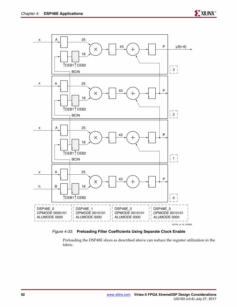
92 www.xilinx.com Virtex-5 FPGA XtremeDSP Design ConsiderationsUG193 (v3.6) July 27, 2017
Chapter 4: DSP48E ApplicationsR
Preloading the DSP48E slices as described above can reduce the register utilization in the fabric.
Figure 4-33: Preloading Filter Coefficients Using Separate Clock Enable
UG193_c4_32_032806
h
x
A
P
25
18
A
P
x
x
25
18
A
P43
x
y3[n-6]
25
18
CEB2CEB1
CEB2CEB1
CEB2
BCIN
BCIN
BCIN
CEB1
CEB2CEB1
A
B
P
DSP48E_0OPMODE 0000101ALUMODE 0000
DSP48E_1OPMODE 0010101ALUMODE 0000
DSP48E_2OPMODE 0010101ALUMODE 0000
DSP48E_3OPMODE 0010101ALUMODE 0000
25
18
P
43
43
43
0
1
2
3

Virtex-5 FPGA XtremeDSP Design Considerations www.xilinx.com 93UG193 (v3.6) July 27, 2017
Application ExamplesR
Pattern Detect ApplicationsThe pattern detector is used to find a perfect match between the DSP48E output and a specified pattern or its complement. A mask field can be used to mask out certain bit locations in the pattern detector. The pattern field and the mask field are 48 bits wide.
The pattern detector allows the DSP48E slice to support convergent rounding and counter auto reset when a count value has been reached and support overflow/underflow/saturation in accumulators. In conjunction with the logic unit, the pattern detector can be extended to a 48-bit dynamic comparison of two 48-bit fields, e.g., (A:B NAND C == Pattern). Another use of the pattern detect circuit is in packet processing and payload matching in networking applications. The following section describes how these applications are implemented in the DSP48E slice.
The following attributes should be set when the pattern detector is being used.
The use of the pattern detector leads to a moderate speed reduction on the pattern detect path. The PD output comes out on the same clock cycle as the DSP48E slice output P.
Table 4-3: Attribute Settings for Pattern Detector Use
PATTERN 48-bit field (48'h000000000000)
Pattern to be used for pattern detector.
MASK 48-bit field (48'h3fffffffffff)
Mask to be used for pattern detector. Sets overflow threshold when overflow feature is used.
SEL_PATTERN PATTERN, C (PATTERN) Selects pattern to be used for pattern detector.
SEL_MASK MASK, C (MASK) Selects mask to be used for pattern detector.
USE_PATTERN_DETECT PATDET Attribute determines if the pattern detector is being used (PATDET) or not (NO_PATDET). This attribute is used for speed specification and simulation model purposes only.
SEL_ROUNDING_MASK SEL_MASK, MODE1,
MODE2 (SEL_MASK)
Selects special masks that can be used for symmetric or convergent rounding uses of the pattern detector. This attribute takes precedence over the SEL_MASK attribute.
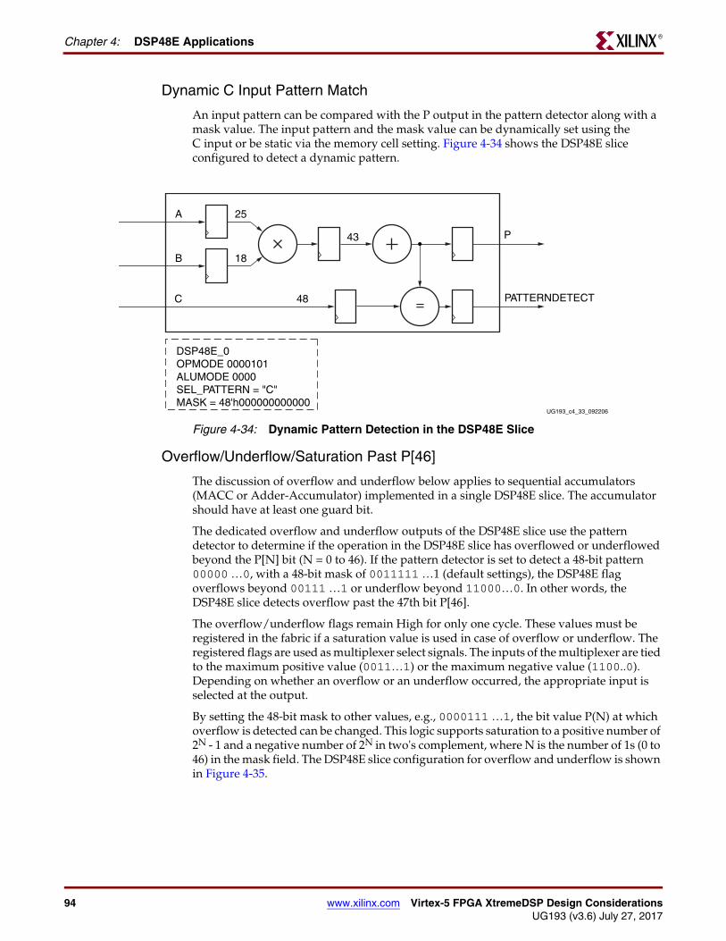
94 www.xilinx.com Virtex-5 FPGA XtremeDSP Design ConsiderationsUG193 (v3.6) July 27, 2017
Chapter 4: DSP48E ApplicationsR
Dynamic C Input Pattern Match
An input pattern can be compared with the P output in the pattern detector along with a mask value. The input pattern and the mask value can be dynamically set using the C input or be static via the memory cell setting. Figure 4-34 shows the DSP48E slice configured to detect a dynamic pattern.
Overflow/Underflow/Saturation Past P[46]
The discussion of overflow and underflow below applies to sequential accumulators (MACC or Adder-Accumulator) implemented in a single DSP48E slice. The accumulator should have at least one guard bit.
The dedicated overflow and underflow outputs of the DSP48E slice use the pattern detector to determine if the operation in the DSP48E slice has overflowed or underflowed beyond the P[N] bit (N = 0 to 46). If the pattern detector is set to detect a 48-bit pattern 00000 …0, with a 48-bit mask of 0011111 …1 (default settings), the DSP48E flag overflows beyond 00111 …1 or underflow beyond 11000…0. In other words, the DSP48E slice detects overflow past the 47th bit P[46].
The overflow/underflow flags remain High for only one cycle. These values must be registered in the fabric if a saturation value is used in case of overflow or underflow. The registered flags are used as multiplexer select signals. The inputs of the multiplexer are tied to the maximum positive value (0011…1) or the maximum negative value (1100..0). Depending on whether an overflow or an underflow occurred, the appropriate input is selected at the output.
By setting the 48-bit mask to other values, e.g., 0000111 …1, the bit value P(N) at which overflow is detected can be changed. This logic supports saturation to a positive number of 2N - 1 and a negative number of 2N in two's complement, where N is the number of 1s (0 to 46) in the mask field. The DSP48E slice configuration for overflow and underflow is shown in Figure 4-35.
Figure 4-34: Dynamic Pattern Detection in the DSP48E Slice
UG193_c4_33_092206
A
B
25
43 P
DSP48E_0OPMODE 0000101ALUMODE 0000SEL_PATTERN = "C"MASK = 48'h000000000000
18
48C =PATTERNDETECT

Virtex-5 FPGA XtremeDSP Design Considerations www.xilinx.com 95UG193 (v3.6) July 27, 2017
Application ExamplesR
Overflow/Underflow/Saturation Past P[47]
Overflow and underflow on the 48th bit can be determined by using the pattern detector and a single LUT in the fabric. The maximum value of a multiply operation in the DSP48E slice is a 43-bit value. A pattern detector can be used to detect OVERFLOW/UNDERFLOW by setting the pattern to be 01111XXX… X (largest positive number) or 10000XXXX …X (largest negative number). Detection of these two numbers is a strong indication that the DSP48E slice could overflow/underflow in the next cycle. Thus, if 01111XXX…X is detected by the pattern_detect and the sign bit of the next computation is 1, then the DSP48E slice has overflowed. Similarly, if 10000XXX…X is detected by the pattern_b_detect and the sign bit of the next computation is 0, the DSP48E slice has underflowed. The pattern_detect output and the sign bit of the next computation is used in the fabric to determine the overflow/underflow status of the DSP48E slice past the 48th bit. The DSP48E configuration is the same as in Figure 4-35.
Overflow/underflow calculations for add-accumulate operations can also be implemented in the same way, provided the bit size of the add is less than that of the accumulate function. For a 36-bit add (sign extended to 48 on the input side) accumulated with a 48-bit accumulate value, the pattern detector is set to simultaneously search for 011111111111XXXX…X and its complement. This implementation does not use the dedicated OVERLOW/UNDERFLOW pins.
Logic Unit and Pattern Detect
The logic unit used in conjunction with the pattern detector has a variety of possible applications. The pattern detector can be used to detect whether a function implemented in the logic unit matches a pattern. If the pattern detector is set to detect a 48-bit pattern 00…0 with a 48-bit mask of 00…0, the pattern detector can detect if all of the results of the logic unit operations are zeros. The pattern_detect logic searches for the all 0s case, and the pattern_b_detect looks for the all 1s case. So (A:B fxn C) == 1 and (A:B fxn C) == 0 can be detected using pattern_detect and pattern_b_detect, e.g., A:B NAND C == 0, A:B OR C == 0, etc.
If the logic unit itself is programmed to perform an XNOR function then the pattern_detect output is effectively the single bit result of a 48-bit match operation between two dynamic 48-bit inputs: C and A:B. This is an alternative implementation of the dynamic pattern match.
Figure 4-35: Overflow/Underflow Detection Using Pattern Detector
UG193_c4_34_092106
A
B
25
43 P
DSP48E_0OPMODE 0100101ALUMODE 0000
18
=
PATTERNDETECT/OVERFLOW/UNDERFLOW

96 www.xilinx.com Virtex-5 FPGA XtremeDSP Design ConsiderationsUG193 (v3.6) July 27, 2017
Chapter 4: DSP48E ApplicationsR
The C input can feed into the pattern detector. When the C input is fed into the pattern detector, any function between the Z multiplexer output and the X multiplexer output can be compared with the dynamic C input value.
With C input connected to the pattern detector, PCIN XNOR A:B == C is implemented, as in Figure 4-36.
If the DSP48E slice is configured to do a subtraction and the pattern detector is used, then C > A:B and C == A:B can be simultaneously detected. The sign bit of the P output indicates if A:B is > or < than C. The PD output indicates if A:B – C == 0. See Figure 4-37.
The pattern detector can be used to check overflow and underflow conditions for 12-bit and 24-bit adders in the SIMD mode. If the logic unit is used in a four 12-bit SIMD mode, a pattern such as 00x…x00x….x00x….x00x….x can detect if any of the 12-bit adders has overflowed or underflowed beyond its respective 11th bit. The pattern detector in this case can only identify if any one of the adders caused an overflow/underflow flag. It cannot identify which one of the four adders caused this flag.
Figure 4-36: PCIN fxn A:B ==C Implementation Using Pattern Detector
Figure 4-37: Comparator Implementation Using Pattern Detector
UG193_c4_35_091806
A
B
30
48XNOR
A:B P
DSP48E_0OPMODE 0010011ALUMODE 0101
48C
PCIN
PD=
UG193_c4_36_010609
A
B
30
48A:B P
DSP48E_0OPMODE 0110011ALUMODE 0011
48C = PATTERNDETECT
18
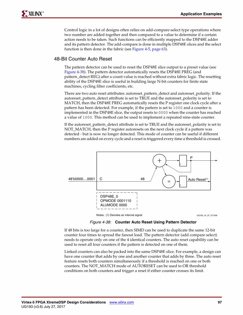
Virtex-5 FPGA XtremeDSP Design Considerations www.xilinx.com 97UG193 (v3.6) July 27, 2017
Application ExamplesR
Control logic in a lot of designs often relies on add-compare-select type operations where two number are added together and then compared to a value to determine if a certain action needs to be taken. Such functions can be efficiently mapped to the DSP48E adder and its pattern detector. The add-compare is done in multiple DSP48E slices and the select function is then done in the fabric (see Figure 4-5, page 63).
48-Bit Counter Auto Reset
The pattern detector can be used to reset the DSP48E slice output to a preset value (see Figure 4-38). The pattern detector automatically resets the DSP48E PREG (and pattern_detect REG) after a count value is reached without extra fabric logic. The resetting ability of the DSP48E slice is useful in building large N-bit counters for finite state machines, cycling filter coefficients, etc.
There are two auto reset attributes: autoreset_pattern_detect and autoreset_polarity. If the autoreset_pattern_detect attribute is set to TRUE and the autoreset_polarity is set to MATCH, then the DSP48E PREG automatically resets the P register one clock cycle after a pattern has been detected. For example, if the pattern is set to 1000 and a counter is implemented in the DSP48E slice, the output resets to 0000 when the counter has reached a value of 1000. This method can be used to implement a repeated nine-state counter.
If the autoreset_pattern_detect attribute is set to TRUE and the autoreset_polarity is set to NOT_MATCH, then the P register autoresets on the next clock cycle if a pattern was detected - but is now no longer detected. This mode of counter can be useful if different numbers are added on every cycle and a reset is triggered every time a threshold is crossed.
If 48 bits is too large for a counter, then SIMD can be used to duplicate the same 12-bit counter four times to spread the fanout load. The pattern detector (add compare select) needs to operate only on one of the 4 identical counters. The auto reset capability can be used to reset all four counters if the pattern is detected on one of them.
Linked counters can also be packed into the same DSP48E slice. For example, a design can have one counter that adds by one and another counter that adds by three. The auto reset feature resets both counters simultaneously if a threshold is reached on one or both counters. The NOT_MATCH mode of AUTORESET can be used to OR threshold conditions on both counters and trigger a reset if either counter crosses its limit.
Figure 4-38: Counter Auto Reset Using Pattern Detector
UG193_c4_37_071006
P
Auto Reset(1)
DSP48E_0OPMODE 0001110ALUMODE 0000
48C48’b0000....0001=
Notes: (1) Denotes an internal signal

98 www.xilinx.com Virtex-5 FPGA XtremeDSP Design ConsiderationsUG193 (v3.6) July 27, 2017
Chapter 4: DSP48E ApplicationsR
Rounding ApplicationsDifferent styles of rounding can be done efficiently in the DSP48E slice. The C port in the DSP48E slice is used to mark the location of the decimal point. For example, if C = 000...00111, this indicates that there are four digits after the decimal point. In other words, the number of continuous ones in the C port bus plus 1 indicates the number of decimal places in the original number.
The CARRYIN input can be used to determine which rounding technique is implemented. If CARRYIN is 1, then C + CARRYIN = 0.5 or 0.1000 in binary. If CARRYIN is zero, then C + CARRYIN = 0.4999... or 0.0111 in binary. Thus, the CARRYIN bit decides if the number is rounded up or rounded down.
The CARRYIN bit and the C input bus can change dynamically. After the round is performed by adding C and CARRYIN to the result, the bits to the right of the decimal point should be discarded.
For convergent rounding, the pattern detector can be used to determine whether a midpoint number is rounded up or down. Truncation is performed after adding C and CARRYIN to the data.
Rounding Decisions
There are different factors to consider while implementing a rounding function:
• Dynamic or static decimal point
• Symmetric or Random or Convergent
• LSB Correction or Carrybit Correction (if convergent rounding was chosen)
Dynamic or Static Decimal Point
This refers to whether the decimal point is fixed in every computation or changes from clock cycle to clock cycle. Most of the techniques described in this section are for static decimal points. These techniques can easily be used for dynamically moving decimal point cases.
Symmetric Rounding
In symmetric rounding towards infinity, the CARRYIN bit is set to the sign bit bar of the result. This ensures that the midpoint negative and positive numbers are both rounded away from zero. For example, 2.5 rounds to 3 and -2.5 rounds to -3. In symmetric rounding towards zero, the CARRYIN bit is set to the sign bit of the result. Positive and negative numbers at the midpoint are rounded towards zero. For example, 2.5 rounds to 2 and -2.5 rounds to -2. Although the round towards infinity is the conventional Matlab round, the round towards zero has the advantage of never causing overflow. Table 4-4 and Table 4-5 shows examples of symmetric rounding.

Virtex-5 FPGA XtremeDSP Design Considerations www.xilinx.com 99UG193 (v3.6) July 27, 2017
Application ExamplesR
The multiply rounding towards infinity is built into the DSP48E slice where the sign bit bar can be chosen by setting CARRYINSEL to 110 (see Table 1-10).
For MACC and add accumulate operations, it is difficult to determine the sign of the output ahead of time, so the round might cost an extra clock cycle. This extra cycle can be eliminated by adding the C input on the very first cycle using dynamic OPMODE. The sign bit of the last but one cycle of the accumulator can be used for the final rounding operation done in the final accumulate cycle. This implementation is a practical way to save a clock cycle. There is a rare chance that the final accumulate operation can flip the sign of the output from the previous accumulated value.
Random Round
In random rounding, the result is rounded up or down. In order to randomize the error due to rounding, one can dynamically alternate between symmetric rounding towards infinity and symmetric rounding towards zero by toggling the CARRYIN bit pseudo-randomly. The CARRYIN bit in this case is a random number. The DSP48E slice adds either 0.4999 or 0.50 to the result before truncation. For example, 2.5 can round to 2 or to 3, randomly. Repeatability depends on how the pseudo-random number is generated. If the LFSR/seed is always the same, then results can be repeatable. Otherwise, the results might not be exactly repeatable.
Convergent Rounding
In convergent rounding, the final result is rounded to the nearest even number (or odd number). In conventional implementations, if the midpoint is detected, then the units-placed bit before the round needs to be examined in order to determine whether the number is going to be rounded up or down. The original number before the round can
Table 4-4: Round to Zero (Decimal Place = 4)
Multiplier Output C CARRYIN = Sign Bit Fabric Out = Multiplier Out + C + Sign Bit
0010.1000(2.5) 0000.0111 0 0010.1111 (2 after Truncation)
1101.1000(-2.5) 0000.0111 1 1110.0000(-2 after Truncation)
0011.1000(3.5) 0000.0111 0 0011.1111(3 after Truncation)
Table 4-5: Round to Infinity (Decimal Place = 4)
Multiplier Output CCARRYIN = Sign Bit
ComplementFabric Out = Multiplier Out + C + Sign Bit
Complement
0010.1000(2.5) 0000.0111 1 0011.1111 (3 after Truncation)
1101.1000(-2.5) 0000.0111 0 1101.1111(-3 after Truncation)
0011.1000(3.5) 0000.0111 1 0100.0000 (4 after Truncation)

100 www.xilinx.com Virtex-5 FPGA XtremeDSP Design ConsiderationsUG193 (v3.6) July 27, 2017
Chapter 4: DSP48E ApplicationsR
change between even/odd from cycle to cycle, so the CARRYIN value cannot be determined ahead of time.
In convergent rounding towards even, the final result is rounded toward the closest even number, for example:
2.5 rounds to 2 and -2.5 rounds to -2, but 1.5 rounds to 2 and -1.5 rounds to -2.
In convergent rounding towards odd, the final result is rounded toward the closest odd number, for example:
2.5 rounds to 3 and -2.5 rounds to -3, but 1.5 rounds to 1 and -1.5 rounds to -1.
The convergent rounding techniques require the use of fabric in addition to the DSP48E slice. There are two ways of implementing a convergent rounding scheme.
• LSB Correction Technique: In the LSB correction technique, a logic gate is needed in fabric to compute the final LSB after rounding.
• Carry Correction Technique: In the carry correction technique, an extra bit is produced by the pattern detector that needs to be added to the truncated output of the DSP48E slice in order to determine the final rounded number. If a series of computations are being performed, then this carry bit can be added in a subsequent fabric add or DSP48E add on the flowing datapath.
The bits after the multiplier should not be rounded because the DSP48E MACC is 48 bits. Even though fabric designs round to allow a 36-bit fabric ACC, this style of coding is inefficient when using the DSP48E slice.
A saturate (SAT) and round (RND) function can be provided by adding a single DSP48E slice and using the PatternDetector of the preceding DSP48E slice to detect the SAT condition. The new extra DSP48E slice should then be used to multiplex maximum positive/negative numbers when a SAT occurs. The extra DSP48E slice PatternDetect should be used as described in “Convergent Rounding: LSB Correction Technique,” page 101 to perform the RND function. This combination never overflows due to rounding because the SAT function takes priority over RND.
When either the FIR filter cascade or MACC precision is 36 bits, PatternDetector and PatternBarDetector can be used instead of the Overflow/Underflow signals. This allows for the full 48-bit precision to be maintained in the Acumulator/P-cascade with sign-extension even if only 36-bit precision is used. For 36-bit precision, the user sets the MASK and PATTERN values as:
MASK = 0x0007 FFFF FFFF
PATTERN = 0x0000 0000 0000
For a 36-bit signed number, the 36th bit is the sign bit which is sign-extended to a full 48-bit word. Therefore, PatternDetector or PATTERNBDETECT (PBD) should always be asserted because the upper 13 bits should be all 1s or all 0s. If the upper 13 bits are not all 1s or all 0s, an underflow or overflow condition has occurred. The SAT signal is defined as:
SAT = (~(PatternDetector) AND ~(PatternBarDetector))
If SAT is asserted and P(47)=1, an underflow has occurred. If SAT is asserted and P(47)=0, an overflow has occurred.
P(47:0) must be routed in fabric to the A:B(47:0) input to provide a pipeline stage because full speed is only possible when the OPMODE and CARRYIN registers are used. The OPMODE of the SAT/RND DSP48E slice is:
OPMODE(7:0)=(0 SAT SAT 0 0 ~SAT ~SAT)

Virtex-5 FPGA XtremeDSP Design Considerations www.xilinx.com 101UG193 (v3.6) July 27, 2017
Application ExamplesR
Thus, the A:B path is selected if there is no SAT condition, while the C port is selected if there is a SAT condition. The C port provides the maximum positive number for saturation.
C = 0x0007 FFFF FFFF
CarryIn = (~(PatternDetector) AND ~(PatternBarDetector)) AND P(47)
Therefore, the most positive SAT number is changed to the most negative SAT number if it is an underflow via the CarryIn path.
MAX Positive = 0x0007 FFFF FFFF
MAX Negative = 0x0008 0000 0000
These are the PatternDetector parameters for the SAT/RND DSP slice for this 36-bit example where the final result is a 12-bit number after rounding:
PATTERN = 0x0000 0000 0000
MASK = 0xFFFF FF00 0000
The convergent round to even constant for 12-bit (Decimal 24) data from 36-bit data input is:
RND CNST = 0x0000 0080 0000
This constant includes the CarryIn listed in Table 4-6, page 103 so that the CarryIn can be used for negative maximum number operation. This constant must be input at the start of an FIR filter cascade or at the beginning of a MACC FIR filter.
The LSB correction method uses the gate described in Figure 4-40, page 102 which is fed by PSAT(24) of the SAT/RND DSP slice. Thus, the 12-bit MSB is PSAT(35).
Convergent Rounding: LSB Correction Technique
For static convergent rounding, the pattern detector can be used to detect the midpoint case. For example, in an 8-bit round, if the deicmal pace is set at 4, the C input should be set to “0000.0111.” Round to odd rounding should use CARRYIN = "0" and check for PATTERN "XXXX.1111" and then replace the units place bit with 1 if the pattern is matched. Round to even rounding should use CARRYIN = "1," check for PATTERN "XXXX.0000," and replace the units place with 0 if the pattern is matched. The DSP48E configuration to implement the convergent rounding is shown in Figure 4-39.

102 www.xilinx.com Virtex-5 FPGA XtremeDSP Design ConsiderationsUG193 (v3.6) July 27, 2017
Chapter 4: DSP48E ApplicationsR
For dynamic convergent rounding, the SEL_PATTERN attribute should be set to PATTERN, and the PATTERN attribute should be set to all zeros. The SEL_ROUNDING_MASK attribute should be set to MODE1 (see Table 1-3). MODE1 sets the pattern detector to look at the decimal fraction. This attribute sets the mask to left shift by 1 of C complement. This makes the mask change dynamically with the C input decimal point. So when the C input is 0000.0111, the mask is 1111.0000.
If the CARRYIN bit is set to a static '1', dynamic convergent round to even can be performed by forcing the LSB of the final value to '0' whenever the PATTERNDETECT output is High. If the CARRYIN bit is set to a static '0', dynamic convergent round to odd can be performed by forcing the LSB of the final value to '1' whenever the PATTERNBDETECT output is High. This is shown in Figure 4-40.
Note that while the PATTERNDETECT searches for XXXX.0000, the PATTERNBDETECT searches for a match with XXXX.1111. The pattern detector is used here to detect the midpoint (special case where decimal fraction is 0.5).
Examples of Dynamic Round to Even and Round to Odd are shown in Table 4-6 and Table 4-7.
Figure 4-39: Convergent Rounding: LSB Correction
Figure 4-40: A: Round to Even and B: Round to Odd
UG193_c4_38_092206
A
B
25
43 P
Use PD toFORCE_LSB
in fabricDSP48E_0OPMODE 0110101ALUMODE 0000
18
C = PD
UG193_c4_39_052306
LSB in from DSP48E Slice
PDLSB
A
LSB in from DSP48E Slice
PBDLSB
B
A: Round to Even B: Round to Odd

Virtex-5 FPGA XtremeDSP Design Considerations www.xilinx.com 103UG193 (v3.6) July 27, 2017
Application ExamplesR
Dynamic Convergent Rounding: Carry Correction Technique
Convergent rounding using carry correction technique requires a check on the units place bit as well as the decimal fraction in order to make the correct decision. The pattern detector is set to detect xxxx0.1111 for the round to odd case. For round to even, the pattern detector detects xxxx1.1111. For the static case, whenever a pattern is detected, a '1' should be added to the P output of the DSP48E slice. This addition can be done in the fabric or another DSP48E slice. If the user has a chain of computations to be done on the data stream, the carry correction style might fit into the flow better than the LSB correction style. The DSP48E implementation is shown in Figure 4-41.
Table 4-6: Round to Even (Pattern = xxxx.1111, Decimal Place = 4)
Multiplier Output C CARRYINMultiplier Out
+ C + CARRYIN
PATTERNDETECT(PD)
Fabric Out (LSB replaced by 0)
0010.1000(2.5) 0000.0111 1 0011.0000 1 0010.0000
(2 after Truncation)
1101.1000(-2.5) 0000.0111 1 1110.0000 1 1110.0000
(-2 after Truncation)
0011.1000(3.5) 0000.0111 1 0100.0000 1 0100.0000
(4 after Truncation)
1110.1000(-1.5) 0000.0111 1 1111.0000 1 1110.0000
(-2 after Truncation)
Table 4-7: Round to Odd (Pattern = xxxx.0000, Decimal Place = 4)
Multiplier Output C CARRYINMultiplier Out + C
+ CARRYINPATTERNBDETECT
(PBD)Fabric Out (LSB replaced by 1)
0010.1000(2.5) 0000.0111 0 0010.1111 1 0011.1111 (3 after Truncation)
1101.1000(-2.5) 0000.0111 0 1101.1111 1 1101.1111 (-3 after Truncation)
0011.1000(3.5) 0000.0111 0 0011.1111 1 0011.1111 (3 after Truncation)
1100.1000(-3.5) 0000.0111 0 1100.1111 1 1101.1111 (-3 after Truncation)

104 www.xilinx.com Virtex-5 FPGA XtremeDSP Design ConsiderationsUG193 (v3.6) July 27, 2017
Chapter 4: DSP48E ApplicationsR
For dynamic rounding using carry correction, the implementation is different for round to odd and round to even.
In the dynamic round to even case, when XXX1.1111 is detected, a carry should be generated. The SEL_ROUNDING_MASK should be set to MODE2 (see Table 1-3). MODE2 looks at the units place bit as well as the decimal fraction. This attribute sets the mask to left shift by 2 of C complement. This makes the mask change dynamically with the C input decimal point. So when the C input is 0000.0111, the mask is 1110.0000. If the PATTERN is set to all ones, then the PATTERNDETECT is a '1' whenever XXX1.1111 is detected. The carry correction bit is the PATTERNDETECT output. The PATTERNDETECT should be added to the truncated P output of the next stage DSP48E slice in order to complete the rounding operation.
Examples of dynamic round to even are shown in Table 4-8.
In the dynamic round to odd case, a carry should be generated whenever XXX0.1111 is detected. SEL_ROUNDING_MASK is set to MODE1 (see Table 1-3). This attribute sets the mask to left shift by 1 of C complement. This makes the mask change dynamically with the C input decimal point. So when the C input is 0000.0111, the mask is 1111.0000. If the PATTERN is set to all ones, then the PATTERNDETECT is a '1' whenever XXXX.1111 is detected. The carry correction bit needs to be computed in fabric, depending on the units place bit of the truncated DSP48E output and the PATTERNDETECT signal. The units
Figure 4-41: Convergent Rounding: Carry Correction
UG193_c4_40_092206
A
B
25
43 P
PD used as rounding correction carry bit to next operation
DSP48E_0OPMODE 0110101ALUMODE 0000
18
48C=
PD
Table 4-8: Round to Even (Pattern = xxx1.1111, Decimal Place = 4)
Multiplier Output C P = MultOut + CPATTERNDETECT
(PD) Fabric Out = P + PD
0010.1000(2.5) 0000.0111 0010.1111 0 0010.1111(2 after Truncation)
1101.1000(-2.5) 0000.0111 1101.1111 1 1110.0000(-2 after Truncation)
0001.1000(1.5) 0000.0111 0001.1111 1 0010.0000(2 after Truncation)
1110.1000(-1.5) 0000.0111 1110.1111 0 1110.1111 (-2 after Truncation)

Virtex-5 FPGA XtremeDSP Design Considerations www.xilinx.com 105UG193 (v3.6) July 27, 2017
Reference Design FilesR
place bit after truncation should be a '0' and the PATTERNDETECT should be a '1' in order for the carry correction bit to be a '1'. This carry correction bit should then be added to the truncated P output of the DSP48E slice in order to complete the round.
Examples of static round to odd are shown in Table 4-9.
Reference Design FilesThe reference design files associated with this user guide can be found on the Virtex-5 FPGA page on xilinx.com.
Table 4-9: Static Round to Odd (Pattern = xxx0.1111, Decimal Place = 4
Multiplier Output C P= Mult Out + CPATTERNDETECT
(PD)Fabric Out = P + PD
0010.1000(2.5) 0000.0111 0010.1111 1 0011.1111 (3 after Truncation)
1101.1000(-2.5) 0000.0111 1101.1111 0 1101.1111 (-3 after Truncation)
0011.1000(3.5) 0000.0111 0011.1111 0 0011.1111 (3 after Truncation)
1100.1000(-3.5) 0000.0111 1100.1111 1 1101.1111 (-3 after Truncation)

106 www.xilinx.com Virtex-5 FPGA XtremeDSP Design ConsiderationsUG193 (v3.6) July 27, 2017
Chapter 4: DSP48E ApplicationsR

Virtex-5 FPGA XtremeDSP Design Considerations www.xilinx.com 107UG193 (v3.6) July 27, 2017
R
Chapter 5
DSP48E Software and Tool Support Overview
IntroductionThis chapter summarizes the different software tools available when designing with the DSP48E slice. The following general coding guidelines should be implemented when designing with DSP48E to maximize efficiency and performance:
• All registers in the DSP48E datapath should be used in order to increase performance.
• Avoid asynchronous resets in your design. All the registers in the DSP48E slice are synchronous. Synchronous resets take precedence over clock enables in the DSP registers.
• Instantiate the DSP48E primitive if a synthesis tool can not infer a desired function.
This chapter contains the following sections:
• “DSP48E Instantiation Templates”
• “DSP48E Software Tools”
DSP48E Instantiation TemplatesThe DSP48E slices can be instantiated in a design using Verilog and VHDL.
The Virtex-5 Libraries Guide for HDL Designs includes the Verilog and VHDL instantiation templates for the DSP48E block.
DSP48E Software Tools
Synthesis ToolsGeneral information on DSP48E inference can be found in the “Coding for FPGA Device Flow” chapter of UG626: Synthesis and Simulation Design Guide for the ISE tools, or in the ISE HDL Language templates. In the Arithmetic Support section, there are VHDL and Verilog examples. For information on XST, see UG627: XST User Guide for Virtex-4, Virtex-5, Spartan-3, and New CPLD Devices.
DSP IPAvailable DSP IPs are listed here:
• Multiplier

108 www.xilinx.com Virtex-5 FPGA XtremeDSP Design ConsiderationsUG193 (v3.6) July 27, 2017
Chapter 5: DSP48E Software and Tool Support OverviewR
• Divider
• FIR Filter Compiler
• Floating Point Operators
• FFT
• Turbo Decoder
More information on Xilinx DSP IP can be found on the DSP IP Core web page.
System Generator for DSPSystem Generator for DSP, shown in Figure 5-1, is a system level design tool that is a Blockset for Matlab Simulink. It has different levels of support for the DSP48E slice. You can use DSP IP with DSP48E support, use the DSP48E slice to build custom functions, or use the DSP48E macro to simplify sequential instructions. More information on using the System Generator tool is available in UG640: System Generator for DSP User Guide.
Architecture WizardThe architecture wizard is a GUI design tool in ISE that supports many single DSP48E slice functions. In some cases, these single DSP48E slice functions can be used to create cascaded DSP48E slice functions. The architecture wizard is accessible through the ISE tools and supports the following configurable blocks:
• Accumulator
• Adder/Subtracter
• Multiplier
• Multiplier and Adder/Accumulator
Many of these functions can also be implemented by using Synthesis Inference, which is the preferred method of using the DSP48E slice.
For information on the Architecture Wizard, please see the Architecture Wizard User Guide in the ISE Software Manuals.
Figure 5-1: System Generator for DSP
UG193_c5_01_032806

Virtex-5 FPGA XtremeDSP Design Considerations www.xilinx.com 109UG193 (v3.6) July 27, 2017
DSP48E Software ToolsR
Retargeting Designs from Virtex-4 DSP48 to Virtex-5 DSP48E SlicesThe software implements most of the retargeting needs automatically. The list provided here is for reference:
• The bit width of the A input has been increased to 30. The key impact of this is sign extension.
• In a Virtex-4 device that is being retargeted, a 36 + 48 signed addition using A:B as a 36-bit adder input should sign extend the A[29:0] all the way to the 30th bit in the Virtex-5 device.
• The multiplier size has been increased to 25 x 18 multiplies. The most important retargeting change is that the A input to the DSP48E slice needs to be sign extended at least up to A[24]. In other words, the sign bit A[17] also needs to be connected to multiple pins A [24:18]. Pins A[29:25] are “don't cares” for the multiply operations.
• Designs in Virtex-4 devices that use a 25 x 25 signed or a 24 x 24 multiply of unsigned operands now only require two DSP48E slices, instead of four DSP48 slices. The asymmetrical multiply also offers advantages for FFT and single precision floating point multiplies.
• The shared C input in Virtex-4 devices has been replaced with a unique C input and C register per DSP48E in Virtex-5 devices. Each DSP48E slice has a unique clock enable (CEC) and reset (RSTC).
• The CARRYINSEL signal is three bits wide in the Virtex-5 FPGA. This signal was two bits wide in Virtex-4 devices.
• Retargeting Virtex-4 FPGA designs to Virtex-5 FPGA designs requires changes in the CARRYINSEL signal. When Virtex-4 CARRYINSEL[1:0] is connected GND or VCC, software can perform this retargeting:
• If CARRYINSEL[1:0] = "00"
• If CARRYINSEL[1:0] = "10”
• If CARRYINSEL[1:0] = "11"
• If CARRYINSEL[1:0] = "01"
• If CARRYINSEL [1:0] signal is dynamic, it is not possible to retarget in software. However, every operation in the Virtex-4 device is supported in the Virtex-5 device. A dynamic CARRYINSEL function in the Virtex-4 device can be implemented in the Virtex-5 device, with the user making the necessary changes to the code.
• The SUBTRACT input in the Virtex-4 device has been replaced with four ALUMODE signals. Designs that use a SUBTRACT = 1 in Virtex-4 devices need to be retargeted accordingly by setting all four ALUMODE bits to 4'b0011. Similarly SUBTRACT = 0 in Virtex-4 devices correspond to ALUMODE = 4'b0000.
• BCASCREG is a new attribute in Virtex-5 devices. In Virtex-4 devices, the number of registers in the B cascade path was the same as the number of registers in the B direct path. So when retargeting Virtex-4 designs to Virtex-5 designs, the BCASCREG attribute should be set to the same value as the BREG attribute (refer to Table 1-11, page 36 in for more details on BCASCREG and BREG attributes). Note that this is different than the default setting of BCASCREG and so retargeting needs to specifically set the BCASCREG attribute. The A input cascade path did not exist in the Virtex-4 FPGA, so the retargeting issue does not exist for ACASCREG attribute.
• The pattern detector is a new feature and so older designs should have the USE_PATTERN_DETECT set to NO_PATDET (which is the default).

110 www.xilinx.com Virtex-5 FPGA XtremeDSP Design ConsiderationsUG193 (v3.6) July 27, 2017
Chapter 5: DSP48E Software and Tool Support OverviewR
• Designs that do not use the multiplier should set the USE_MULT attribute to “NONE” in order to save power by shutting down the multiplier. The USE_MULT is a new attribute in the Virtex-5 device that replaces the LEGACY_MODE attribute in Virtex-4 device.
• Subtractreg in the Virtex-4 device should map to Alumodereg - similarly CECINSUB (in the Virtex-4 device) should map to both CEALUMODE (in the Virtex-5 device) and CECARRYIN (in the Virtex-5 device).
• RSTCTRL (in the Virtex-4 device) should map to both RSTCTRL and RSTALUMODE in the Virtex-5 device.
• The “CECARRYIN” signal for the Virtex-5 DSP48E slice has a completely different meaning than the Virtex-4 device. Virtex-4 designs should retarget Virtex-4 DSP48's CECARRYIN onto the Virtex-5 device’s CEMULTCARRYIN and should retarget Virtex-4 device’s CECINSUB onto both the CECARRYIN and the CEALUMODE in the Virtex-5 device.
Education CoursesXilinx Education Services offers comprehensive, flexible training solutions designed to help you get your product to market quickly and efficiently. The following classes contain information about using the Virtex-5 DSP48E XtremeDSP slice.
• DSP Design Flows
• DSP Implementation Techniques
• Achieving Breakthrough Performance in Virtex-4 FPGAs
Education Home page:http://www.xilinx.com/training/index.htm
Application NotesFor application examples targeted to Virtex-5 devices, refer to Chapter 2, “DSP48E Design Considerations.”

Virtex-5 FPGA XtremeDSP Design Considerations www.xilinx.com 111UG193 (v3.6) July 27, 2017
R
Appendix A
CARRYOUT, CARRYCASCOUT, and MULTSIGNOUT
CARRYOUT/CARRYCASCOUTThe DSP48E slice and the fabric carry chain use a different implementation style for subtract functions. The carry chain implementation in the CLB slices requires the fabric carry input pin to be connected to a constant 1 during subtract operations. The standard subtract operation with ALUMODE = 0011 in the DSP48E slice does not require the CARRYIN pin to be set to 1.
In two's complement notation, negative values are obtained by performing a bitwise inversion and adding one, e.g., -B = ((not B) + 1). The CLB implements A-B as (A + (not B) + 1), as shown in Figure A-1. An alternate implementation of a two-input subtracter is [not (B + (not A))], as shown in Figure A-2. The alternate implementation allows the carry inputs to the adder/subtracter to still be available for normal use.
Figure A-1: Fabric-based Adder/Subtracter
+A
B
0
Carry Input
A + B
UG193_A_01_092107
0
1
+A
B
Sub/Add = 1/0
(Carry input must be 1 for a subtract operation, so it is not available for other uses.)
A ± B
0
1

112 www.xilinx.com Virtex-5 FPGA XtremeDSP Design ConsiderationsUG193 (v3.6) July 27, 2017
Appendix A: CARRYOUT, CARRYCASCOUT, and MULTSIGNOUTR
The DSP48E slice uses the second implementation extended to 3-input adders with a CARRYIN input as shown in Figure A-3. This allows DSP48E SIMD operations to perform subtract operations without a carryin for each smaller add/sub unit.
ALUMODE 0000/0011 implements Z ± (CIN + X + Y). ALUMODE = 0011 corresponds to Virtex®-4 DSP48 Subtract=1.ALUMODE = 0000 corresponds to Virtex-4 DSP48 Subtract=0.
Virtex-5 ALUMODE supports additional subtract operations:
ALUMODE 0001 implements (-Z + (X + Y + CIN) – 1).
• For most uses, CIN is set to 1 to cancel out the -1.
Figure A-2: Adder/Subtracter with Optional Carry Inputs
Figure A-3: DSP48E Slice Three-Input Adder
UG193_A_02_091607
+B
A
Sub/add
Opt. carry input
(Carryin available as an input even for subtract operations)
A +/– (B + optional carry input)
0
1
0
1
UG193_A_03_092107
+Y
X
Z
ALUMODE[0]
CIN
ALUMODE[1]
DSP48E Slice Add/Subtract
0
1
0
1

Virtex-5 FPGA XtremeDSP Design Considerations www.xilinx.com 113UG193 (v3.6) July 27, 2017
MULTSIGNOUT and CARRYCASCOUTR
ALUMODE 0010 actually implements -(Z + X + Y + CIN) – 1.
• This inversion of the P output obtained by using ALUMODE 0010 can be cascaded to another slice to implement a two’s complement subtract.
For add operations, CARRYOUT[3] and CARRYCASCOUT are identical, but the convention used to indicate a borrow (for subtract operations) is different. CARRYOUT[3] matches the convention for fabric subtractions. The matched convention allows a fabric add-sub function to use the CARRYOUT[3] pin directly to extend two-input DSP48E slice subtract operations in the fabric. The CARRYCASCOUT, however, follows the subtract convention of DSP slices and is, therefore, ideal for cascading up vertically to another DSP slice.
These CARRYOUT[3] and CARRYCASCOUT signals enable the construction of higher precision add/sub functions using multiple DSP48E slices or using a hybrid approach with both a DSP48E slice and a fabric adder/subtracter.
MULTSIGNOUT and CARRYCASCOUTCARRYOUT[3] should not be used for multiply operations because the first stage multiplier generates two partial products, which are added together in the second stage of the DSP48E slice.
All DSP three-input add operations (including Multiply-Add and Multiply Accumulate) actually produce two carryout bits for retaining full precision. This is shown in Figure A-3.
MULTSIGNOUT and CARRYCASCOUT serve as the two carry bits for MACC_EXTEND operations. If MULTSIGNOUT is the multiplier sign bit and CARRYCASCOUT is the cascaded carryout bit, the result is the software/Unisim model abstraction, shown in Figure A-4.
MULTSIGNOUT and CARRYCASCOUT in the simulation model do not match the hardware, but the output P bits do match for supported functions, such as MACC_EXTEND. For example, routing CARRYCASCOUT to the fabric by using all zeroes in the upper DSP slice does not match the CARRYOUT[3] of the lower DSP slice. Similarly, MULTSIGNOUT routed out to fabric is not actually the sign of the multiply result.
These MULTSIGNOUT and CARRYCASCOUT signals enable the construction of higher precision multiply-accumulate (MACC_EXTEND) functions, such as a 25x18 multiply accumulated for up to 96 bits of accumulator precision and running at the maximum DSP48E slice frequency.
It is also necessary to set the OPMODEREG and CARRYINSEL to 1 when building large accumulators such as the 96-bit Multiply Accumulate. This prevents the simulation model from propagating unknowns to the upper DSP48E slice when a reset occurs.
Figure A-4: DSP48E Slice Three-Input Adder
UG193_A_04_092107
+Y
X
Z P[47:0]
CIN
One Bit Carry Out to FabricCARRYOUT[3]
Two bits of carryout are produced in the hardware and are labeled as MULTSIGNOUT and CARRYCASCOUT in the simulation model.

114 www.xilinx.com Virtex-5 FPGA XtremeDSP Design ConsiderationsUG193 (v3.6) July 27, 2017
Appendix A: CARRYOUT, CARRYCASCOUT, and MULTSIGNOUTR
Summary of Appendix A
Adder/Subtracter-only OperationCARRYOUT[3]: Hardware and software match.
CARRYCASCOUT: Hardware and software match when ALUMODE=0000 and inverted when ALUMODE=0011. The mismatch happens because the DSP48E slice performs the subtract operation using a different algorithm from the fabric; thus, the DSP48E slice requires an inverted carryout from the fabric.
MULTSIGNOUT is invalid in adder-only operation.
MACC OperationCARRYOUT[3] is invalid in the MACC operation.
CARRYCASCOUT and MULTSIGNOUT: Hardware and software do not match due to modeling difference. The software simulation model is an abstraction of the hardware model. The software views of CARRYCASCOUT and MULTSIGNOUT enable higher-precision MACC functions to be built in the Unisim model. They are not logically equivalent to hardware CARRYCASCOUT and MULTSIGNOUT. Only the hardware and software results (P output) are logically equivalent. The internal signals (CARRYCASCOUT and MULTSIGNOUT) are not. See Figure A-5.
Figure A-5: MACC Software and Hardware Models
UG193_A_05_100207
+A
B
Partial products from the multiply operation are added together in the second stage ternary adder.
CARRYCASCOUT
MULTSIGNOUT
x
Hardware Implementation
Software Model
+A
B
CARRYIN
Zmux (e.g., C, P, PCIN)
CARRYCASCOUT
MULTSIGNOUT
x
CARRYIN
Zmux (e.g., C, P, PCIN)
P[47:0]
P[47:0]