Embed Size (px)
Citation preview
1
Wafer-scale, full-coverage, acoustic self-limiting assembly of
particles on flexible substrates
Liang Zhao1,2, Bchara Sidnawi1,3#, Jichao Fan4#, Ruiyang Chen4, Thomas Scully1,2, Scott
Dietrich5, Weilu Gao4, Qianhong Wu1,3, Bo Li1,2,*
1 Department of Mechanical Engineering, Villanova University, Villanova, PA 19085, USA.
2 Hybrid Nano-Architectures and Advanced Manufacturing Laboratory, Villanova University,
Villanova, PA, 19085, USA
3 Cellular Biomechanics and Sports Science Laboratory, Villanova University, Villanova, PA,
19085, USA
4 Department of Electrical and Computer Engineering, University of Utah, Salt Lake City UT,
84112, USA
5 Department of Physics, Villanova University, Villanova, PA, 19085, USA
# These authors contributed equally to this work.
* Corresponding author: [email protected]
2
Self-limiting assembly of particles represents the state-of-the-art controllability in
nanomanufacturing processes where the assembly stops at a designated stage1,2,
providing a desirable platform for applications requiring delicate thickness
control3-5. Most successes in self-limiting assembly are limited to self-assembled
monolayers (SAM) of small molecules on inorganic, chemically homogeneous rigid
substrates (e.g., Au and SiO2) through surface-interaction mechanisms6,7. Similar
mechanisms, however, cannot achieve uniform assembly of particles on flexible
polymer substrates8,9. The complex configurations and conformations of polymer
chains create a surface with non-uniform distributions of chemical groups and
phases. In addition, most assembly mechanisms require good solvent wettability,
where many desirable but hard-to-wet particles and polymer substrates are
excluded. Here, we demonstrate an acoustic self-limiting assembly of particles
(ASAP) method to achieve wafer-scale, full-coverage, close-packed monolayers of
hydrophobic particles on hydrophobic polymer substrates in aqueous solutions.
We envision many applications in functional coatings and showcase its feasibility
in structural coloration.
Self-assembled monolayers (SAM) of molecules and particles show significant potentials in
applications such as molecular junctions10-12, ultrathin dielectrics13,14, chemical and biosensors15,16,
adjustable wetting/protection coatings17-19, and medicine20. SAM was originally developed for
molecules based on the self-limiting chemisorption process, which involves an accurate chemical
design to create the buffer layer as a bridge between the substrate and SAM-molecules21,22. When
nano- or micro-particles are decorated with the SAM-molecules, self-limiting assembly of
particles on target substrates can be achieved23. To achieve high-quality assembly with densely
3
packed structures, a molecular-level chemically uniform surface of the substrate is required24.
However, for polymers with complex configurations and conformations, it is extremely difficult
to control the distribution of chemical groups or phases (e.g., amorphous and crystalline region for
semicrystalline polymers)25. To improve the chemical uniformity, mechanical stretching has been
utilized9. Unfortunately, high-density and low-defect assembly on flexible polymer substrates is
yet to be achieved for both molecules8,9 and molecule-decorated particles25,26. Although chemical
treatments can be used to modify the surface properties of particles and polymer substrates, a
uniform chemical treatment for polymers remains a significant challenge. In contrast to previous
“chemical” strategies, our ASAP method explores a physical-process-based self-limiting strategy,
utilizing interfacial energy design and viscoelastic energy dissipation in flexible polymers, where
the assembly process is facilitated by acoustic and flow fields to realize high-rate, close-packed
assembly of nano-/microparticles on polymer substrates.
The assembly process is outlined in Fig. 1a. In contrast to the SAM created by chemisorption
of molecules with head groups interacting with the substrate27, ASAP represents a new assembly
mechanism based on physical interactions. The hydrophobic monodisperse silica (SiO2) particles
with a very narrow size distribution are dispersed and agitated by the acoustic field (frequency =
40 kHz, power density = 0.3 W cm-2) in water solution to collide with a moving
poly(dimethylsiloxane) (PDMS, Sylgard 184) substrate driven by a customized dipping system to
provide cyclic dipping (Supplementary Fig. 1). The viscoelastic polymer substrate will attenuate
the particle’s kinetic energy upon collision, after which hydrophobic particles tend to stay on the
hydrophobic substrate to minimize their surface energy in the water solution. Once the first particle
layer forms, it becomes a hard shell on the substrate and prevents further deposition, leading to a
self-limiting monolayer assembly. Such a mechanism relies on hard-to-wet surface energy design,
4
acoustic-field-induced particle dispersion and energization, the fluid shearing at the substrate’s
surface, and viscoelastic polymer substrate dissipating the kinetic energy of particles. The
functions of acoustic and shear fields will be discussed separately in the following section. A
representative hard-to-wet assembly system is designed: de-ionized water as solvent, hydrophobic
PDMS as the substrate, and hydrophobic monodisperse SiO2 particles (three diameters: d = 487±10
nm, 761±25 nm, and 1007±29 nm). The characterization of particle sizes by scanning electron
microscope (SEM) and atomic force microscope (AFM) can be found in Supplementary
Information Fig. 2. The hydrophobicity of the particles enables them to adhere to the soft PDMS
substrate due to the lower surface energy between their surface and the substrate. This is
corroborated by our previous assembly work on a wide range of hydrophobic nanomaterials (e.g.,
graphene, h-BN, carbon black, and carbon nanotube) on hydrophobic polymer substrates (e.g.,
PDMS and thermoplastic polyurethan). It was demonstrated that nanomaterials with a wide size
distribution can only achieve multilayer assembly28,29. Here, we use monodispersed SiO2 particles
to achieve uniform monolayer assembly. The as-received SiO2 particles are hydrophilic. They are
later modified with (3-aminopropyl) triethoxysilane (APTES) to create a hydrophobic surface (See
surface chemistry and wettability characterization in Supplementary Figs. 3 and 4). Figs. 1b and c
demonstrate a close-packed monolayer of SiO2 particles (d = 761 nm) on a flat PDMS substrate
and the coverage (𝛿) of the assembly can reach 98.35%. Note that a patch on which particles are
closely packed is considered fully covered, since no further material can fill the residual voids
dictated by the particles’ spherical geometry. The concentration (𝐶0) of particle suspension is 10
mg ml-1 and the assembly time (t) is 900 seconds. Note, the pristine hydrophilic SiO2 particles can
achieve little assembly following identical procedures (Supplementary Fig. 5). The same principles
can be extended to organic particles such as poly (methyl methacrylate) (PMMA) particles (d = 5
5
μm) (Supplementary Fig. 6a). Such self-limiting mechanism is not sensitive to the geometry of the
substrate. We have demonstrated the conformal coating of SiO2 particles (d = 761 nm) on a PDMS
microfiber (d = 6 µm) (Fig. 1d) and PMMA particles (d = 5 μm) on microtrenched PDMS
(Supplementary Fig. 6b). Importantly, ASAP can be implemented within a roll-to-roll process to
enable wafer-scale manufacturing as shown in Fig. 1e, Supplementary Fig. 7, and Supplementary
Video 1. The assembled monolayer of SiO2 particles (d = 761 nm) shows a uniform orange color
(Fig. 1f) when illuminated with white light from the background, highlighting its potential for
structural coloration.
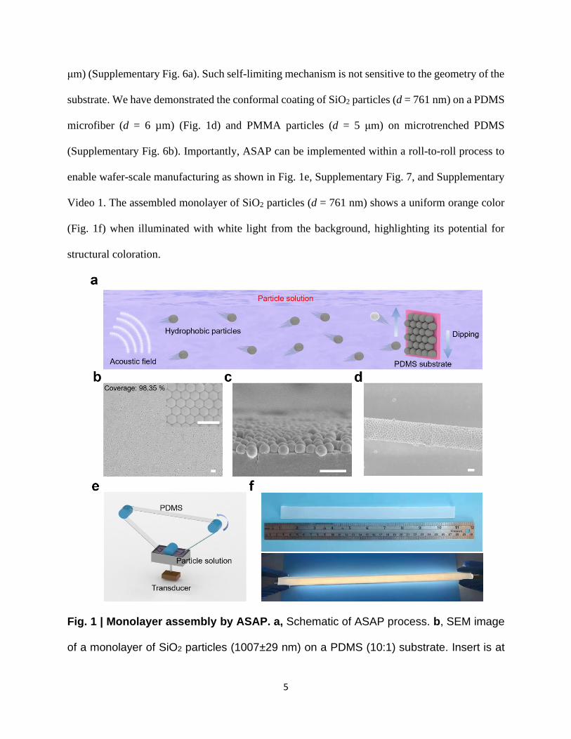
Fig. 1 | Monolayer assembly by ASAP. a, Schematic of ASAP process. b, SEM image
of a monolayer of SiO2 particles (1007±29 nm) on a PDMS (10:1) substrate. Insert is at
6
high-magnification and displays the local hexagonal structure of the particles. c, The
cross-sectional view of monolayer SiO2 particles. d, Monolayer SiO2 particles assembled
on PDMS (10:1) fiber. All scale bars, 2 μm. e, Schematic of large-scale manufacturing of
monolayer SiO2 particles on PDMS substrate. f, Photo of resulting large-area monolayer
of SiO2 particles on a PDMS substrate (top) and the produced orange color from a white
light source (bottom).
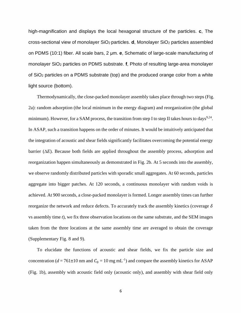
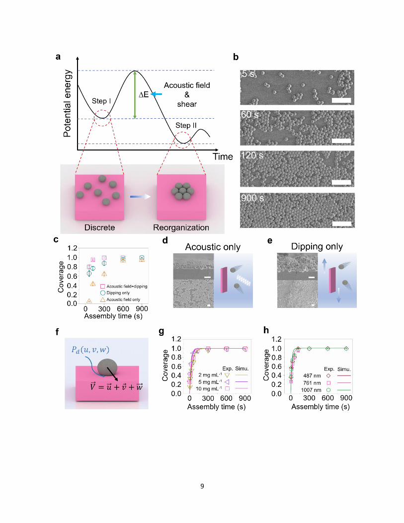
Thermodynamically, the close-packed monolayer assembly takes place through two steps (Fig.
2a): random adsorption (the local minimum in the energy diagram) and reorganization (the global
minimum). However, for a SAM process, the transition from step I to step II takes hours to days9,24.
In ASAP, such a transition happens on the order of minutes. It would be intuitively anticipated that
the integration of acoustic and shear fields significantly facilitates overcoming the potential energy
barrier (∆E). Because both fields are applied throughout the assembly process, adsorption and
reorganization happen simultaneously as demonstrated in Fig. 2b. At 5 seconds into the assembly,
we observe randomly distributed particles with sporadic small aggregates. At 60 seconds, particles
aggregate into bigger patches. At 120 seconds, a continuous monolayer with random voids is
achieved. At 900 seconds, a close-packed monolayer is formed. Longer assembly times can further
reorganize the network and reduce defects. To accurately track the assembly kinetics (coverage 𝛿
vs assembly time t), we fix three observation locations on the same substrate, and the SEM images
taken from the three locations at the same assembly time are averaged to obtain the coverage
(Supplementary Fig. 8 and 9).
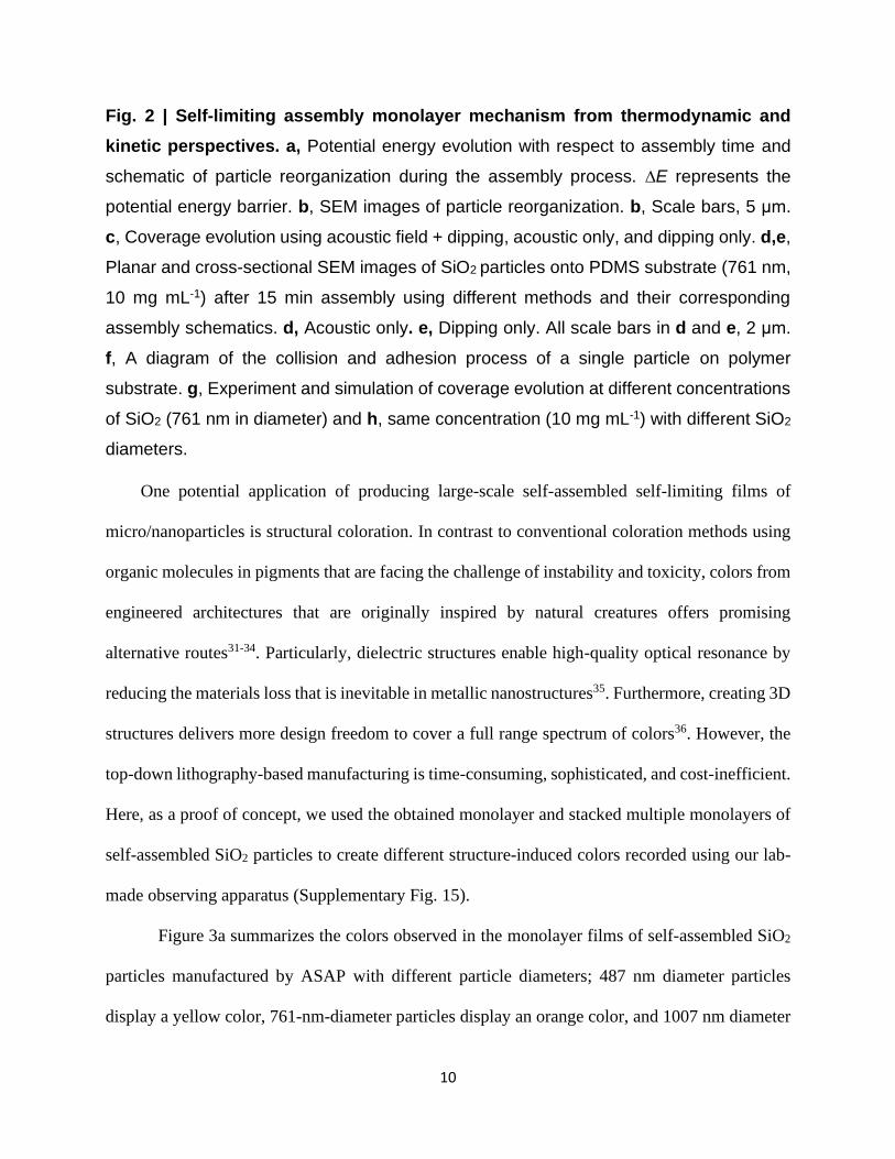
To elucidate the functions of acoustic and shear fields, we fix the particle size and
concentration (d = 761±10 nm and 𝐶0 = 10 mg mL-1) and compare the assembly kinetics for ASAP
(Fig. 1b), assembly with acoustic field only (acoustic only), and assembly with shear field only
7
(dipping only) (Fig. 2c-2e and Supplementary Fig. 8 and 9c). The other assembly parameters are
similar among the three while we simply turn off the dipping motor (acoustic only) or acoustic
transducer (dipping only). The comparison suggests that ASAP, combining both acoustic and shear
fields, leads to the fastest assembly (Fig. 2c). For morphology comparison at the same assembly
time (t = 900 seconds), ASAP leads to a close-packed assembly (Fig. 1b), while acoustic-only
process results in partial coverage (Fig. 2d) and dipping-only process leads to multilayer assembly
(Fig. 2e). The acoustic effect prevents particle aggregation in the solution, and therefore keeps
them from stacking up as clumps on the substrate (top image, Fig. 2d). Coverage, however, is
abated by the absence of the shear that would have been provided by cyclic dipping. The shear on
the substrate’s surface helps the particles penetrate the thinning water film separating from the
substrate during their collision with it, therefore enhancing the coverage as shown in Fig. 2e.
However, a monolayer can be hardly observed (top image, Fig. 2e). Combining cyclic dipping
with acoustic actuation not only leads to a monolayer covering the entire surface, but also ensures
a faster assembly than one that is driven by either an acoustic field or dipping only.
Figure 2f elaborates the mechanism of ASAP on a polymer substrate. A particle heading
towards the substrate at a velocity vector �⃗⃗� , consisting of a normal component, �⃗⃗� , and in-plane
components �⃗� and 𝑣 , will induce a deformation on the flexible surface upon collision. 𝑔(𝑢, 𝑣, 𝑤)
describes the particles’ velocity distribution prior to surface impact while 𝑃𝑑(𝑢, 𝑣, 𝑤) describes
the particle deposition probability. Another striking particle is much more likely to bounce off an
already assembled monolayer, due to both the hard collision and the acoustic field maintaining
dispersion. The time evolution of the substrate’s covered fraction30, 𝛿(𝑡) = 1 − 𝑒−𝛼𝐶0𝑎𝑝𝑡, depends
on the single particle’s occupied area on the substrate, 𝑎𝑝, the particles’ mass concentration 𝐶0,
and 𝛼 =1
𝑚∫ ∫ ∫ 𝑤𝑔(𝑢, 𝑣, 𝑤)𝑃𝑑(𝑢, 𝑣, 𝑤)𝑑𝑤 𝑑𝑢 𝑑𝑣
∞
0
∞
−∞
∞
−∞, where 𝑚 is the single particle mass. Fig.
8
2g shows representative fitting results of the equation for 𝛿(𝑡), for a particle size of 761 nm at
different concentrations while Fig. 2h shows the same analysis as the one illustrated in Fig. 2g, but
for different particle sizes. All coverage evolution conforms to the expected exponential trend.
The authors note that higher concentrations do not necessarily ensure faster assembly and that an
optimal concentration may exist. Supplemental Figures 11-14 and their associated discussion can
provide some clarification, but a detailed interdependence of the parameters 𝛼, 𝐶0, and 𝑎𝑝 requires
further study. We hypothesize that higher concentrations eventually become detrimental to
𝑔(𝑢, 𝑣, 𝑤) (See expression of 𝛼), thereby slowing down the assembly process. Nevertheless, the
ASAP method achieves monolayer assembly regardless of particle concentration and size within
the testing range.
9
10
Fig. 2 | Self-limiting assembly monolayer mechanism from thermodynamic and
kinetic perspectives. a, Potential energy evolution with respect to assembly time and
schematic of particle reorganization during the assembly process. ∆E represents the
potential energy barrier. b, SEM images of particle reorganization. b, Scale bars, 5 μm.
c, Coverage evolution using acoustic field + dipping, acoustic only, and dipping only. d,e,
Planar and cross-sectional SEM images of SiO2 particles onto PDMS substrate (761 nm,
10 mg mL-1) after 15 min assembly using different methods and their corresponding
assembly schematics. d, Acoustic only. e, Dipping only. All scale bars in d and e, 2 μm.
f, A diagram of the collision and adhesion process of a single particle on polymer
substrate. g, Experiment and simulation of coverage evolution at different concentrations
of SiO2 (761 nm in diameter) and h, same concentration (10 mg mL-1) with different SiO2
diameters.
One potential application of producing large-scale self-assembled self-limiting films of
micro/nanoparticles is structural coloration. In contrast to conventional coloration methods using
organic molecules in pigments that are facing the challenge of instability and toxicity, colors from
engineered architectures that are originally inspired by natural creatures offers promising
alternative routes31-34. Particularly, dielectric structures enable high-quality optical resonance by
reducing the materials loss that is inevitable in metallic nanostructures35. Furthermore, creating 3D
structures delivers more design freedom to cover a full range spectrum of colors36. However, the
top-down lithography-based manufacturing is time-consuming, sophisticated, and cost-inefficient.
Here, as a proof of concept, we used the obtained monolayer and stacked multiple monolayers of
self-assembled SiO2 particles to create different structure-induced colors recorded using our lab-
made observing apparatus (Supplementary Fig. 15).
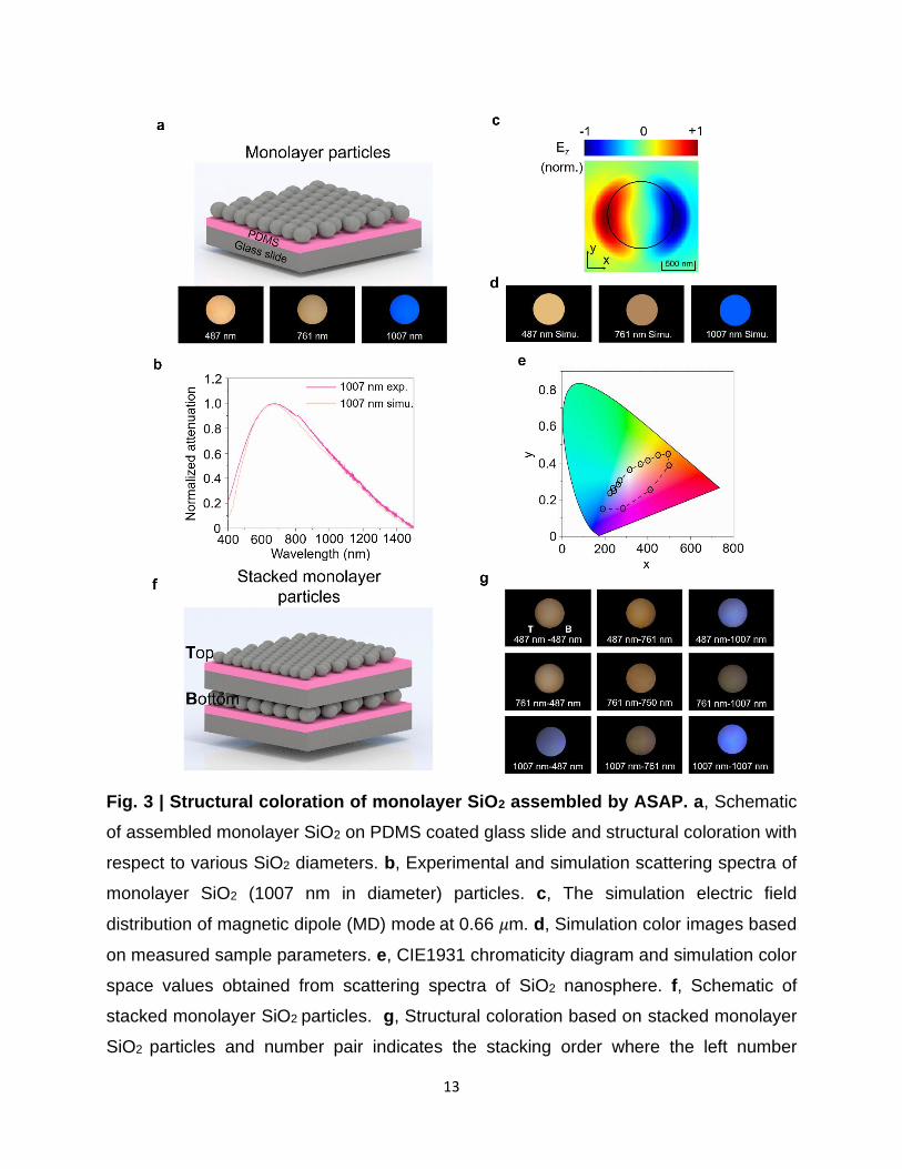
Figure 3a summarizes the colors observed in the monolayer films of self-assembled SiO2
particles manufactured by ASAP with different particle diameters; 487 nm diameter particles
display a yellow color, 761-nm-diameter particles display an orange color, and 1007 nm diameter
11
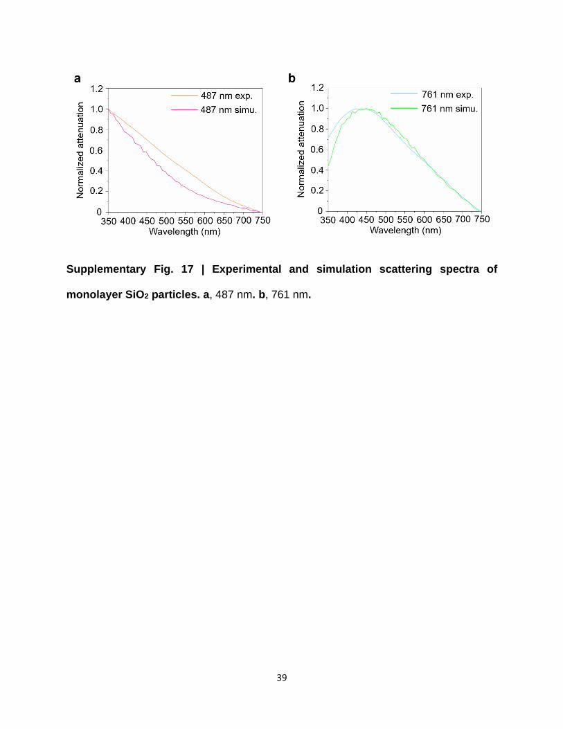
particles display a blue color. The corresponding attenuation spectrum for 1007-nm-diameter
particles is shown in Fig. 3b, where a clear resonance feature is observed. Fig. 3b displays excellent
agreement between finite-difference-time-domain (FDTD) simulation and experimental scattering
spectra of our SiO2 (1007 nm) monolayer particles. The scattering spectra of the other SiO2
monolayer particles with different diameters can be found in Supplementary Fig. 17. Furthermore,
the FDTD-simulated Ez-field profile in x-y plane shown in Fig. 3c when the electromagnetic wave
propagates along z-axis suggests that the structural coloration derives from the magnetic dipole
Mie resonance in the visible range. According to Mie theory37, the resonance peak depends on the
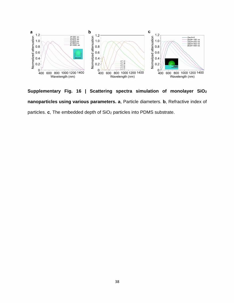
refractive index of materials and scatterer dimensions. In Supplementary Figs. 16a and b, it is clear
that the resonance peak shifts to red with an increasing diameter of nanospheres and refractive
index of materials. During the ASAP assembly process, the particles are accelerated by the acoustic
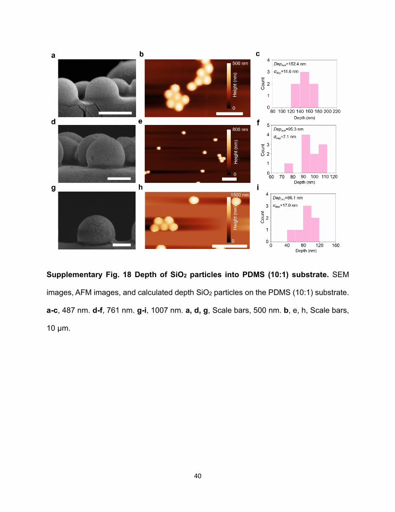
wave and slammed onto the substrate. Considering the viscoelastic elasticity of PDMS substrates,
the particles would get partially embedded inside the substrate (Supplementary Fig. 18). As the
refractive index of SiO2 is close to PDMS, the embedment reduces the effective scattering volume
of particles. Thus, we calculate the depth of SiO2 particles (Ddep) inside the PDMS substrate
(Supplementary Fig. 18). As demonstrated in Supplementary Fig. 16c, the simulated Mie
scattering spectra as a function of Ddep indicate that larger Ddep causes blue shifting of the resonance
peak.
Based on the parameters that can influence the transmission spectra mentioned above, we
measured those parameters by AFM and SEM (Supplementary Fig. 17) and did the calculations of
converting measured and FDTD-simulated transmission spectra to colors. From Fig. 3d, the
calculation results display excellent agreement with experimental structural coloration under white
light illuminiation. Furthermore, we calculate colors for a group of particles with different
12
diameters and plot their color coordinates in CIE 1931 color space; see Fig. 3e. The results show
the color range of monolayer films of particles whose diameters range from 200 nm to 1500 nm.
In addition, we stacked the monolayer samples (Fig. 3f), and experimental colors of different
combinations are summarized in Fig. 3g. The results show that the stacked monolayers can
significantly enrich the color map and the potential to create a full range of coloration.
13
Fig. 3 | Structural coloration of monolayer SiO2 assembled by ASAP. a, Schematic
of assembled monolayer SiO2 on PDMS coated glass slide and structural coloration with
respect to various SiO2 diameters. b, Experimental and simulation scattering spectra of
monolayer SiO2 (1007 nm in diameter) particles. c, The simulation electric field
distribution of magnetic dipole (MD) mode at 0.66 𝜇m. d, Simulation color images based
on measured sample parameters. e, CIE1931 chromaticity diagram and simulation color
space values obtained from scattering spectra of SiO2 nanosphere. f, Schematic of
stacked monolayer SiO2 particles. g, Structural coloration based on stacked monolayer
SiO2 particles and number pair indicates the stacking order where the left number
14
indicates the diameter of the particle on the bottom layer and right number indicates the
diameter of the particle on the top layer. Note, here B and T represent the bottom layer
and top layer with different or same particle sizes according to the stacking sequence.
In summary, ASAP represents a high-quality and scalable self-limiting assembly method to
achieve monolayer particles on flexible polymer substrates. Unlike chemisorption mechanisms for
SAM, ASAP highlights a new assembly mechanism in which physical collision and surface
adhesion between particle and viscoelastic polymer substrates are modulated by acoustic and flow
fields. Such new mechanism is independent of the chemical heterogeneity of polymer substrates
and enables close-packed monolayer particles on polymer. ASAP also unlocks a wide range of
hard-to-wet systems that are desirable but extremely challenging to manufacture. The capability
of accurately controlling the layer numbers of assemblies in wafer scale with full coverage paves
the way towards next-generation flexible optics and wearable electronics.
Author contributions
B. L. conceived, initiated, and supervised the project. L. Z. conceived the experiment and
performed the assembly, structural characterization including all SEM imaging, contact angle
measurement and part of AFM measurement, and structural coloration characterization. B. S.
performed the coverage of assembly and analysis and simulation of the assembly data. J. F.
performed the analysis and simulation of structural coloration. R. C. performed the measurement
of scattering spectra. T. S. constructed the roll-to-roll set-up and performed part of the assembly.
S. D. performed part of AFM measurement. W. G. designed and supervised the optical
measurement and data analysis. Q. W. supervised physics-based modeling. All authors contributed
to writing and revising the manuscript.
Acknowledgments
L.Z., B.S., Q.W. and B.L. were partially supported by the National Science Foundation CMMI
Advanced Manufacturing Program under Award # 2003077. L.Z., and B.L. acknowledge the
startup fund of Villanova University. J. F., R. C., and W. G. acknowledge the startup fund of the
15
University of Utah.
Competing interests
B. L., B. S. and Q. W. have a U.S. Provisional Patent Application on the topic of this paper
(63/135,872, 2021). The other authors declare no competing interests.
References
1 Xia, Y. et al. Self-assembly of self-limiting monodisperse supraparticles from polydisperse
nanoparticles. Nat. Nanotechnol. 6, 580-587 (2011).
2 Hagan, M. F. & Grason, G. M. Equilibrium mechanisms of self-limiting assembly. Rev.
Mod. Phys. 93, 025008 (2021).
3 Wang, J.-L., Lu, Y.-R., Li, H.-H., Liu, J.-W. & Yu, S.-H. Large area co-assembly of
nanowires for flexible transparent smart windows. J. Am. Chem. Soc. 139, 9921-9926
(2017).
4 Lee, T. et al. Controlling the dimension of the quantum resonance in CdTe quantum dot
superlattices fabricated via layer-by-layer assembly. Nat. Commun. 11, 5471 (2020).
5 Kang, K. et al. Layer-by-layer assembly of two-dimensional materials into wafer-scale
heterostructures. Nature 550, 229-233 (2017).
6 Ho, J. C. et al. Controlled nanoscale doping of semiconductors via molecular monolayers.
Nat. Mater. 7, 62-67 (2008).
7 Inayeh, A. et al. Self-assembly of N-heterocyclic carbenes on Au (111). Nat. Commun. 12,
4034 (2021).
8 Gholamrezaie, F. et al. Ordered semiconducting self-assembled monolayers on polymeric
surfaces utilized in organic integrated circuits. Nano Lett. 10, 1998-2002 (2010).
9 Genzer, J. & Efimenko, K. Creating long-lived superhydrophobic polymer surfaces
through mechanically assembled monolayers. Science 290, 2130-2133 (2000).
10 Akkerman, H. B., Blom, P. W., De Leeuw, D. M. & De Boer, B. Towards molecular
electronics with large-area molecular junctions. Nature 441, 69-72 (2006).
11 Tao, N. J. Electron transport in molecular junctions. Nanoscience And Technology: A
Collection of Reviews from Nature Journals, 185-193 (2010).
16
12 Carnegie, C. et al. Flickering nanometre-scale disorder in a crystal lattice tracked by
plasmonic flare light emission. Nat.Commun. 11, 682 (2020).
13 Sekitani, T., Zschieschang, U., Klauk, H. & Someya, T. Flexible organic transistors and
circuits with extreme bending stability. Nat. Mater. 9, 1015-1022 (2010).
14 Klauk, H., Zschieschang, U., Pflaum, J. & Halik, M. Ultralow-power organic
complementary circuits. Nature 445, 745-748 (2007).
15 Calhoun, M., Sanchez, J., Olaya, D., Gershenson, M. & Podzorov, V. Electronic
functionalization of the surface of organic semiconductors with self-assembled monolayers.
Nat. Mater. 7, 84-89 (2008).
16 Litke, J. L. & Jaffrey, S. R. Highly efficient expression of circular RNA aptamers in cells
using autocatalytic transcripts. Nat. Biotechnol. 37, 667-675 (2019).
17 Ren, S. et al. Friction and wear studies of octadecyltrichlorosilane SAM on silicon. Tribol.
Lett. 13, 233-239 (2002).
18 Yu, J. et al. Adaptive hydrophobic and hydrophilic interactions of mussel foot proteins
with organic thin films. Proc. Natl. Acad. Sci. USA 110, 15680-15685 (2013).
19 Horinek, D. & Netz, R. R. Specific ion adsorption at hydrophobic solid surfaces. Phys. Rev.
Lett. 99, 226104 (2007).
20 Ohya, Y. et al. Formation of 1D and 2D gold nanoparticle arrays by divalent DNA-gold
nanoparticle conjugates. Small 8, 2335-2340 (2012).
21 Xiang, J., Zhu, P., Masuda, Y. & Koumoto, K. Fabrication of self-assembled monolayers
(SAMs) and inorganic micropattern on flexible polymer substrate. Langmuir 20, 3278-
3283 (2004).
22 Bain, C. D. & Whitesides, G. M. Molecular-level control over surface order in self-
assembled monolayer films of thiols on gold. Science 240, 62-63 (1988).
23 Park, J. S., Lee, Y.-J. & Yoon, K. B. Marked increase in the binding strength between the
substrate and the covalently attached monolayers of zeolite microcrystals by lateral
molecular cross-linking between the neighboring microcrystals. J. Am. Chem. Soc.126,
1934-1935 (2004).
24 Bigioni, T. P. et al. Kinetically driven self assembly of highly ordered nanoparticle
monolayers. Nat. Mater. 5, 265-270 (2006).
17
25 Freeman, R. G. et al. Self-assembled metal colloid monolayers: an approach to SERS
substrates. Science 267, 1629-1632 (1995).
26 Zhang, B., Zhou, M. & Liu, X. Monolayer assembly of oriented zeolite crystals on α‐Al2O3
supported polymer thin films. Adv. Mater. 20, 2183-2189 (2008).
27 Puebla-Hellmann, G., Venkatesan, K., Mayor, M. & Lörtscher, E. Metallic nanoparticle
contacts for high-yield, ambient-stable molecular-monolayer devices. Nature 559, 232-235
(2018).
28 Zhou, D. et al. Sono-assisted surface energy driven assembly of 2D materials on flexible
polymer substrates: A green assembly method using water. ACS Appl. Mater. Interfaces
11, 33458-33464 (2019).
29 Zhou, D. et al. Ultrafast assembly and healing of nanomaterial networks on polymer
substrates for flexible hybrid electronics. Appl. Mater. Today 22, 100956 (2021).
30 Sidnawi, B., Zhou, D., Li, B. & Wu, Q. A physics-based statistical model for nanoparticle
deposition. J. Appl. Phys. 129, 065303 (2021).
31 Zhao, Y., Xie, Z., Gu, H., Zhu, C. & Gu, Z. Bio-inspired variable structural color materials.
Chem. Soc. Rev. 41, 3297-3317 (2012).
32 Kinoshita, S. & Yoshioka, S. Structural colors in nature: the role of regularity and
irregularity in the structure. ChemPhysChem 6, 1442-1459 (2005).
33 Vukusic, P. & Sambles, J. R. Photonic structures in biology. Nature 424, 852-855 (2003).
34 Kim, H. et al. Structural colour printing using a magnetically tunable and lithographically
fixable photonic crystal. Nat. Photonics 3, 534-540 (2009).
35 Song, M. et al. Colors with plasmonic nanostructures: A full-spectrum review. Appl. Phys.
Rev. 6, 041308 (2019).
36 Iwata, M., Teshima, M., Seki, T., Yoshioka, S. & Takeoka, Y. Bio‐inspired bright
structurally colored colloidal amorphous array enhanced by controlling thickness and black
background. Adv. Mater. 29, 1605050 (2017).
37 Hergert, W. & Wriedt, T. The Mie theory: basics and applications. Vol. 169 (Springer,
2012).
18
Supplementary Information
Wafer-scale, full-coverage, acoustic self-limiting assembly of
particles on flexible substrates
Liang Zhao1,2, Bchara Sidnawi1,3#, Jichao Fan4#, Ruiyang Chen4, Thomas Scully1,2, Scott Dietrich5,
Weilu Gao4, Qianhong Wu1,3, Bo Li1,2,*
1 Department of Mechanical Engineering, Villanova University, Villanova, PA 19085, USA.
2 Hybrid Nano-Architectures and Advanced Manufacturing Laboratory, Villanova University,
Villanova, PA, 19085, USA
3 Cellular Biomechanics and Sports Science Laboratory, Villanova University, Villanova, PA,
19085, USA
4 Department of Electrical and Computer Engineering, University of Utah, Salt Lake City UT,
84112, USA
5 Department of Physics, Villanova University, Villanova, PA, 19085, USA
# These authors contributed equally to this work.
* Corresponding author: [email protected]
19
Methods:
Modification of SiO2 particles
Three kinds of monodisperse silicon dioxide (SiO2) spheres (Sigma; 500 nm, 750 nm, 1000 nm)
are employed in this work. The diameters are further precisely determined by SEM images. The
results show that the average diameters are 487±10 nm, 761±25 nm, and 1007±29 nm, respectively.
Because of the intrinsic hydrophilicity of SiO2, we use (3-aminopropyl)triethoxysilane to modify
it and transfer it into hydrophobicity. Briefly, 100 mg SiO2 particles are added into10 mL ethanol,
followed by sonication for 5 min. Then the solution is heated in an oil bath at 60 ℃ for 48 h. The
resulted solution finally is centrifuged for 5 times (each time for 5 min).
Self-limiting assembly of monolayer
Polydimethylsiloxane film (PDMS) is fabricated on the surface of glass slide (1 inch × 1 inch)
using spin-coating method. The ratio of monomer and cross-linking agent is adjusted to 10:1 in
volume. Note, this is for the assembly of SiO2 particles, but 20:1 for PMMA particle assembly.
The PDMS fiber is prepared by stretching the uncured PDMS on a glass slide (heated to 100 ℃).
The patterned PDMS is made in a patterned Si wafer mold. Before assembly, the as-prepared
hydrophobic particle solution is heated to 50 ℃ and kept in a sonicator. The spin-coated PDMS
substrate then is held in the holder of a lab-made dip coater. During the dipping process, the
sonication is applied, and the sample is immersed in the solution all the time.
Structural coloration simulation
To reveal the origin of the structural coloration produced by our ASAP sample, we employed
finite-difference time-domain method to fit experimental spectra of monolayer nanoparticles. To
20
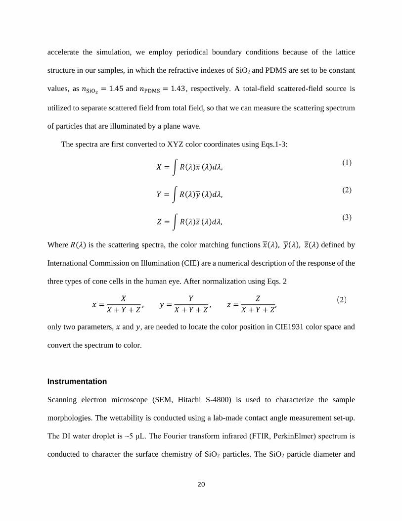
accelerate the simulation, we employ periodical boundary conditions because of the lattice
structure in our samples, in which the refractive indexes of SiO2 and PDMS are set to be constant
values, as 𝑛SiO2= 1.45 and 𝑛PDMS = 1.43, respectively. A total-field scattered-field source is
utilized to separate scattered field from total field, so that we can measure the scattering spectrum
of particles that are illuminated by a plane wave.
The spectra are first converted to XYZ color coordinates using Eqs.1-3:
𝑋 = ∫𝑅(𝜆)𝑥 (𝜆)𝑑𝜆,
(1)
𝑌 = ∫𝑅(𝜆)𝑦 (𝜆)𝑑𝜆,
(2)
𝑍 = ∫𝑅(𝜆)𝑧 (𝜆)𝑑𝜆,
(3)
Where 𝑅(𝜆) is the scattering spectra, the color matching functions 𝑥(𝜆), 𝑦(𝜆), 𝑧(𝜆) defined by
International Commission on Illumination (CIE) are a numerical description of the response of the
three types of cone cells in the human eye. After normalization using Eqs. 2
𝑥 =
𝑋
𝑋 + 𝑌 + 𝑍, 𝑦 =
𝑌
𝑋 + 𝑌 + 𝑍, 𝑧 =
𝑍
𝑋 + 𝑌 + 𝑍,
(2)
only two parameters, 𝑥 and 𝑦, are needed to locate the color position in CIE1931 color space and
convert the spectrum to color.
Instrumentation
Scanning electron microscope (SEM, Hitachi S-4800) is used to characterize the sample
morphologies. The wettability is conducted using a lab-made contact angle measurement set-up.
The DI water droplet is ~5 μL. The Fourier transform infrared (FTIR, PerkinElmer) spectrum is
conducted to character the surface chemistry of SiO2 particles. The SiO2 particle diameter and

21
depth into PDMS are obtained by atomic force microscopy (AFM, Agilent 5500). The scattering
spectra of monolayer SiO2 particles are conducted by Hitachi U4100 UV-Vis-NIR spectrometer.
22
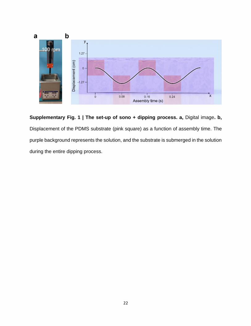
Supplementary Fig. 1 | The set-up of sono + dipping process. a, Digital image. b,
Displacement of the PDMS substrate (pink square) as a function of assembly time. The
purple background represents the solution, and the substrate is submerged in the solution
during the entire dipping process.
23
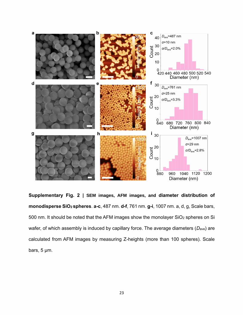
Supplementary Fig. 2 | SEM images, AFM images, and diameter distribution of
monodisperse SiO2 spheres. a-c, 487 nm. d-f, 761 nm. g-i, 1007 nm. a, d, g, Scale bars,
500 nm. It should be noted that the AFM images show the monolayer SiO2 spheres on Si
wafer, of which assembly is induced by capillary force. The average diameters (Dave) are
calculated from AFM images by measuring Z-heights (more than 100 spheres). Scale
bars, 5 μm.
24
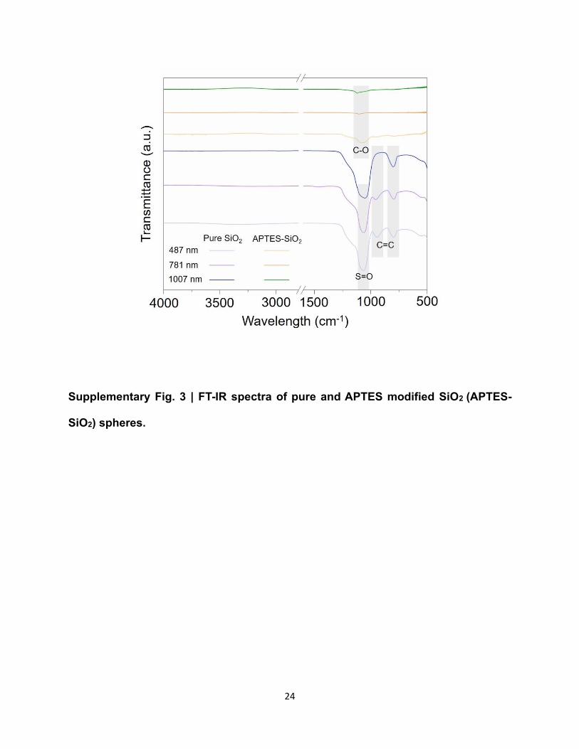
Supplementary Fig. 3 | FT-IR spectra of pure and APTES modified SiO2 (APTES-
SiO2) spheres.
25
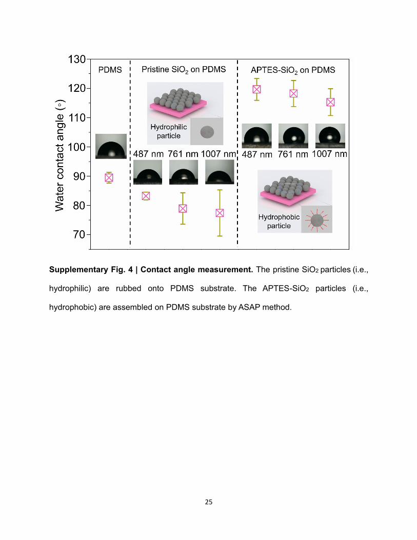
Supplementary Fig. 4 | Contact angle measurement. The pristine SiO2 particles (i.e.,
hydrophilic) are rubbed onto PDMS substrate. The APTES-SiO2 particles (i.e.,
hydrophobic) are assembled on PDMS substrate by ASAP method.
26
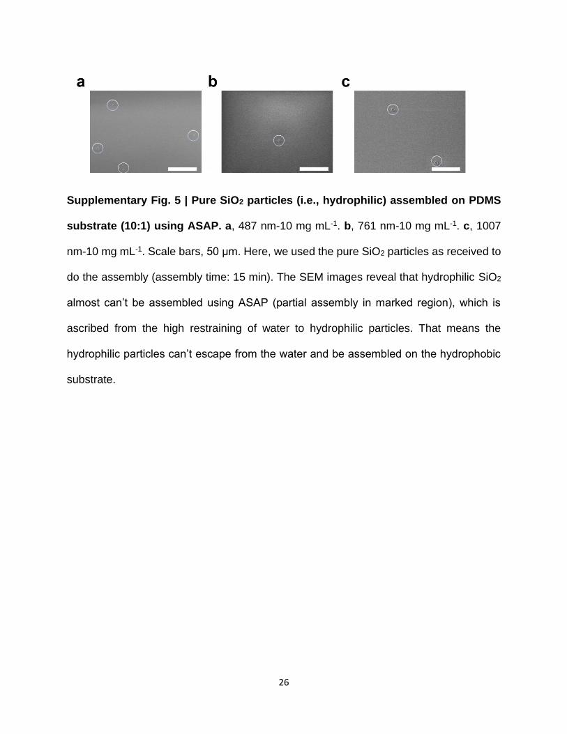
Supplementary Fig. 5 | Pure SiO2 particles (i.e., hydrophilic) assembled on PDMS
substrate (10:1) using ASAP. a, 487 nm-10 mg mL-1. b, 761 nm-10 mg mL-1. c, 1007
nm-10 mg mL-1. Scale bars, 50 μm. Here, we used the pure SiO2 particles as received to
do the assembly (assembly time: 15 min). The SEM images reveal that hydrophilic SiO2
almost can’t be assembled using ASAP (partial assembly in marked region), which is
ascribed from the high restraining of water to hydrophilic particles. That means the
hydrophilic particles can’t escape from the water and be assembled on the hydrophobic
substrate.
27
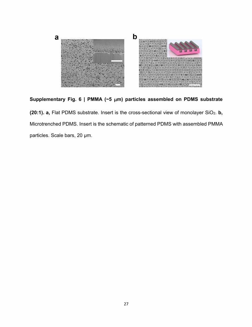
Supplementary Fig. 6 | PMMA (~5 μm) particles assembled on PDMS substrate
(20:1). a, Flat PDMS substrate. Insert is the cross-sectional view of monolayer SiO2. b,
Microtrenched PDMS. Insert is the schematic of patterned PDMS with assembled PMMA
particles. Scale bars, 20 μm.
28
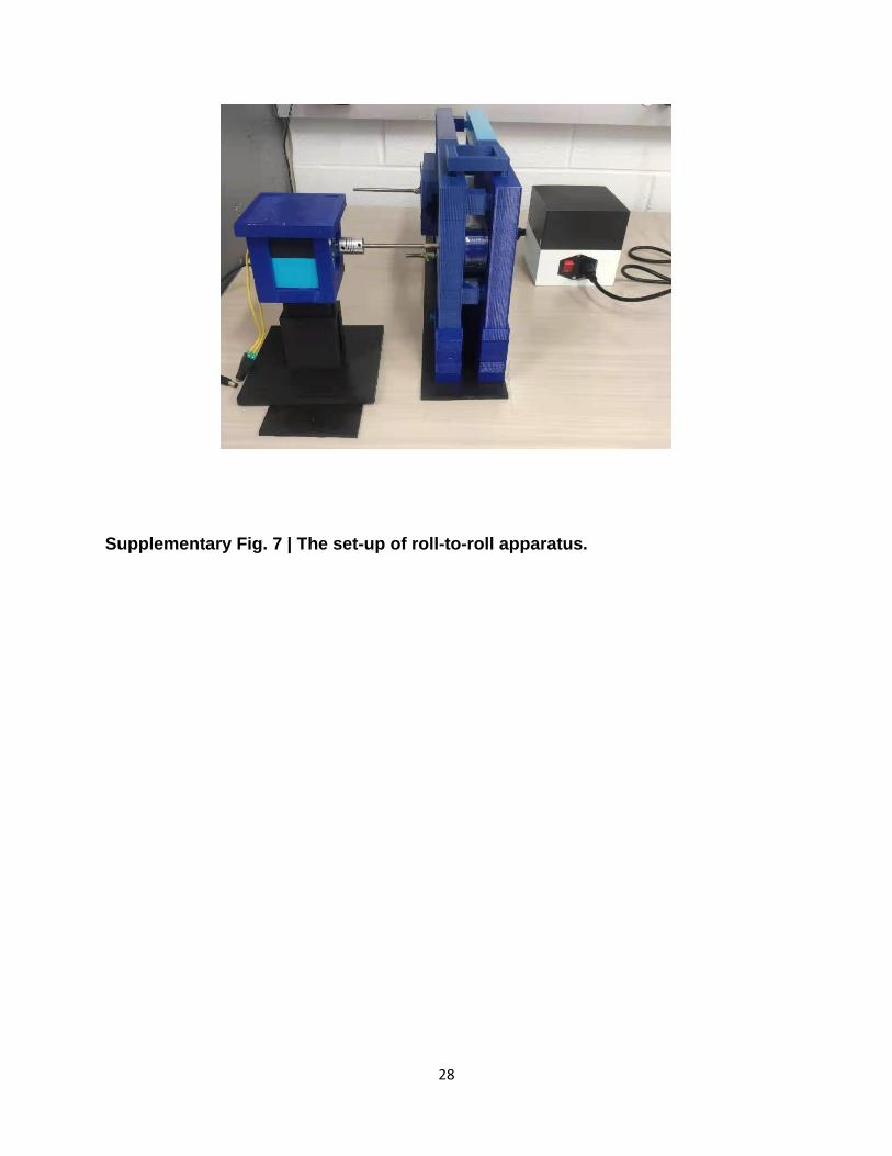
Supplementary Fig. 7 | The set-up of roll-to-roll apparatus.
29
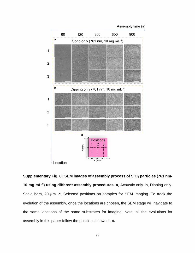
Supplementary Fig. 8 | SEM images of assembly process of SiO2 particles (761 nm-
10 mg mL-1) using different assembly procedures. a, Acoustic only. b, Dipping only.
Scale bars, 20 m. c, Selected positions on samples for SEM imaging. To track the
evolution of the assembly, once the locations are chosen, the SEM stage will navigate to
the same locations of the same substrates for imaging. Note, all the evolutions for
assembly in this paper follow the positions shown in c.
30
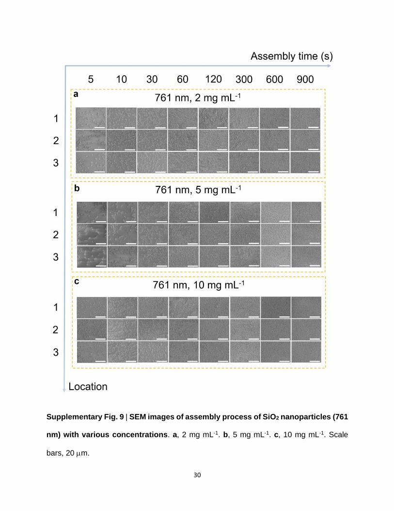
Supplementary Fig. 9 | SEM images of assembly process of SiO2 nanoparticles (761
nm) with various concentrations. a, 2 mg mL-1. b, 5 mg mL-1. c, 10 mg mL-1. Scale
bars, 20 m.
31
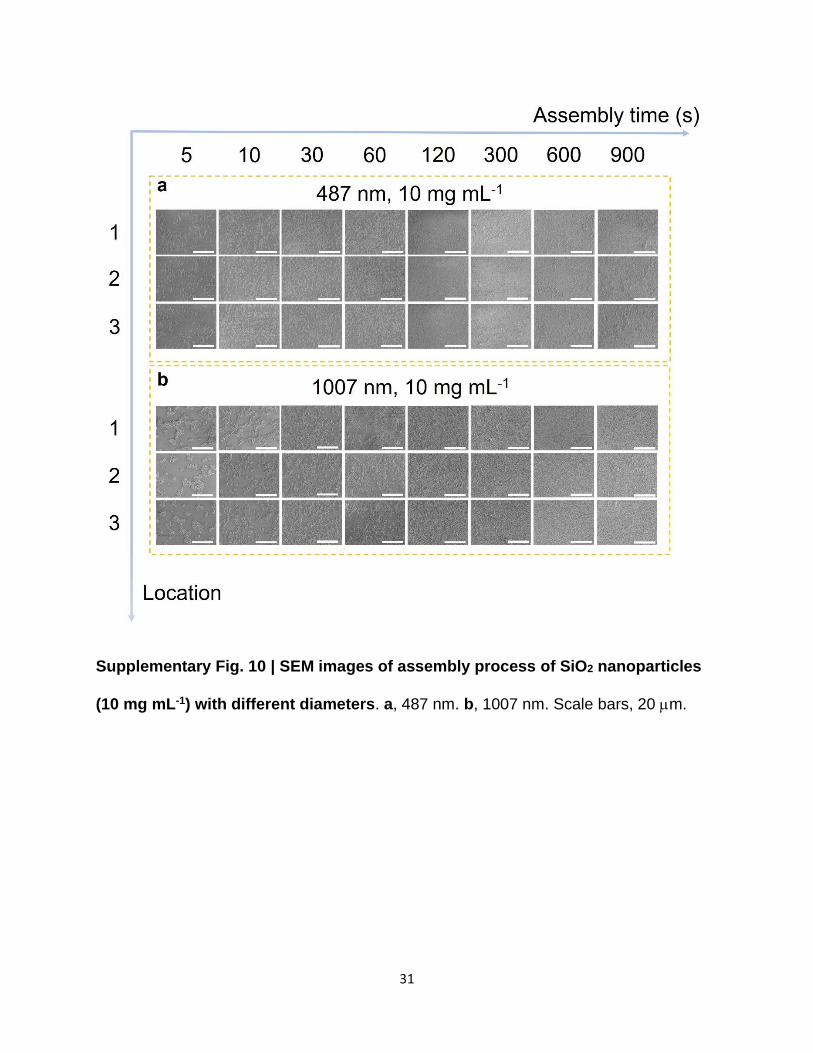
Supplementary Fig. 10 | SEM images of assembly process of SiO2 nanoparticles
(10 mg mL-1) with different diameters. a, 487 nm. b, 1007 nm. Scale bars, 20 m.
32
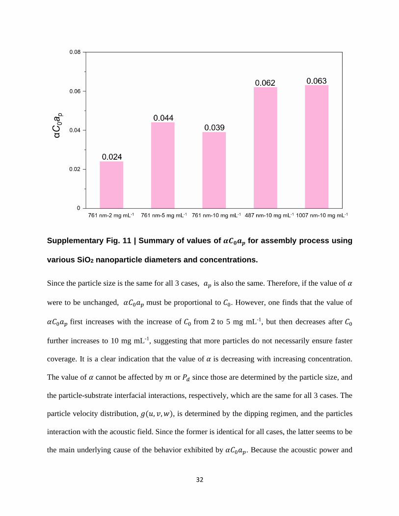
Supplementary Fig. 11 | Summary of values of 𝜶𝑪𝟎𝒂𝒑 for assembly process using
various SiO2 nanoparticle diameters and concentrations.
Since the particle size is the same for all 3 cases, 𝑎𝑝 is also the same. Therefore, if the value of 𝛼
were to be unchanged, 𝛼𝐶0𝑎𝑝 must be proportional to 𝐶0. However, one finds that the value of
𝛼𝐶0𝑎𝑝 first increases with the increase of 𝐶0 from 2 to 5 mg mL-1, but then decreases after 𝐶0
further increases to 10 mg mL-1, suggesting that more particles do not necessarily ensure faster
coverage. It is a clear indication that the value of 𝛼 is decreasing with increasing concentration.
The value of 𝛼 cannot be affected by 𝑚 or 𝑃𝑑 since those are determined by the particle size, and
the particle-substrate interfacial interactions, respectively, which are the same for all 3 cases. The
particle velocity distribution, 𝑔(𝑢, 𝑣, 𝑤), is determined by the dipping regimen, and the particles
interaction with the acoustic field. Since the former is identical for all cases, the latter seems to be
the main underlying cause of the behavior exhibited by 𝛼𝐶0𝑎𝑝. Because the acoustic power and
33
frequency settings were the same for the 3 cases, a quite plausible explanation for this behavior is
the increased dispersion of acoustic energy at higher concentrations. Therefore, for a given particle
size, acoustic settings, and dipping regimen, an optimal concentration that elicits the fastest
assembly, exists. Fig. 2h shows the intermediate particle size of 761 nm leads to the poorest
coverage performance, compared to those corresponding to the other two sizes. Systematic control
of vectorial acoustic field in future experiments will offer more insights into revealing the effect
of particle size. In addition to 𝑎𝑝 being different, different particle sizes imply different values of
𝑚 and 𝑃𝑑 in the expression of 𝛼. Also, it is worth noting that the particle size relative to the
wavelength of the sound waves is crucial to its interaction with the acoustic field, which affects
𝑔(𝑢, 𝑣, 𝑤). Therefore, future experiments, in which the acoustic field is systematically controlled,
where frequencies may be such that wavelengths are of comparable size to the particle’s, are
essential to achieve a clear understanding of the size effect.
34
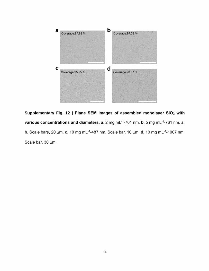
Supplementary Fig. 12 | Plane SEM images of assembled monolayer SiO2 with
various concentrations and diameters. a, 2 mg mL-1-761 nm. b, 5 mg mL-1-761 nm. a,
b, Scale bars, 20 m. c, 10 mg mL-1-487 nm. Scale bar, 10 m. d, 10 mg mL-1-1007 nm.
Scale bar, 30 m.
35
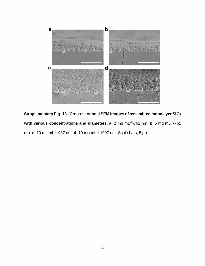
Supplementary Fig. 13 | Cross-sectional SEM images of assembled monolayer SiO2
with various concentrations and diameters. a, 2 mg mL-1-761 nm. b, 5 mg mL-1-761
nm. c, 10 mg mL-1-487 nm. d, 10 mg mL-1-1007 nm. Scale bars, 5 m.
36
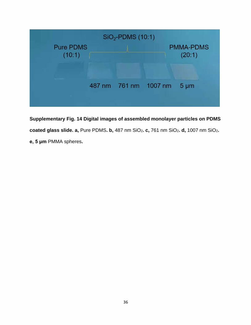
Supplementary Fig. 14 Digital images of assembled monolayer particles on PDMS
coated glass slide. a, Pure PDMS. b, 487 nm SiO2. c, 761 nm SiO2. d, 1007 nm SiO2.
e, 5 μm PMMA spheres.
37
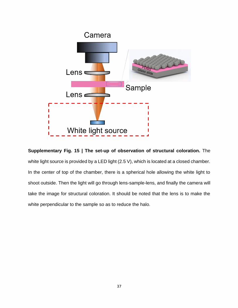
Supplementary Fig. 15 | The set-up of observation of structural coloration. The
white light source is provided by a LED light (2.5 V), which is located at a closed chamber.
In the center of top of the chamber, there is a spherical hole allowing the white light to
shoot outside. Then the light will go through lens-sample-lens, and finally the camera will
take the image for structural coloration. It should be noted that the lens is to make the
white perpendicular to the sample so as to reduce the halo.
38
Supplementary Fig. 16 | Scattering spectra simulation of monolayer SiO2
nanoparticles using various parameters. a, Particle diameters. b, Refractive index of
particles. c, The embedded depth of SiO2 particles into PDMS substrate.
39
Supplementary Fig. 17 | Experimental and simulation scattering spectra of
monolayer SiO2 particles. a, 487 nm. b, 761 nm.
40
Supplementary Fig. 18 Depth of SiO2 particles into PDMS (10:1) substrate. SEM
images, AFM images, and calculated depth SiO2 particles on the PDMS (10:1) substrate.
a-c, 487 nm. d-f, 761 nm. g-i, 1007 nm. a, d, g, Scale bars, 500 nm. b, e, h, Scale bars,
10 μm.