Embed Size (px)
Citation preview
SwitchingStage
SamplingComparator (SC)
OPA615
Biasing
OTA
HoldControl
Emitter2
Collector(IOUT)
12
1S/HIn+
S/HIn−
∞
+VCC −VCC
IQ AdjustSOTA
BaseCHOLDGround
349
7
10
11
13 5
OPA615
www.ti.com...................................................................................................................................... SBOS299E –FEBRUARY 2004–REVISED SEPTEMBER 2009
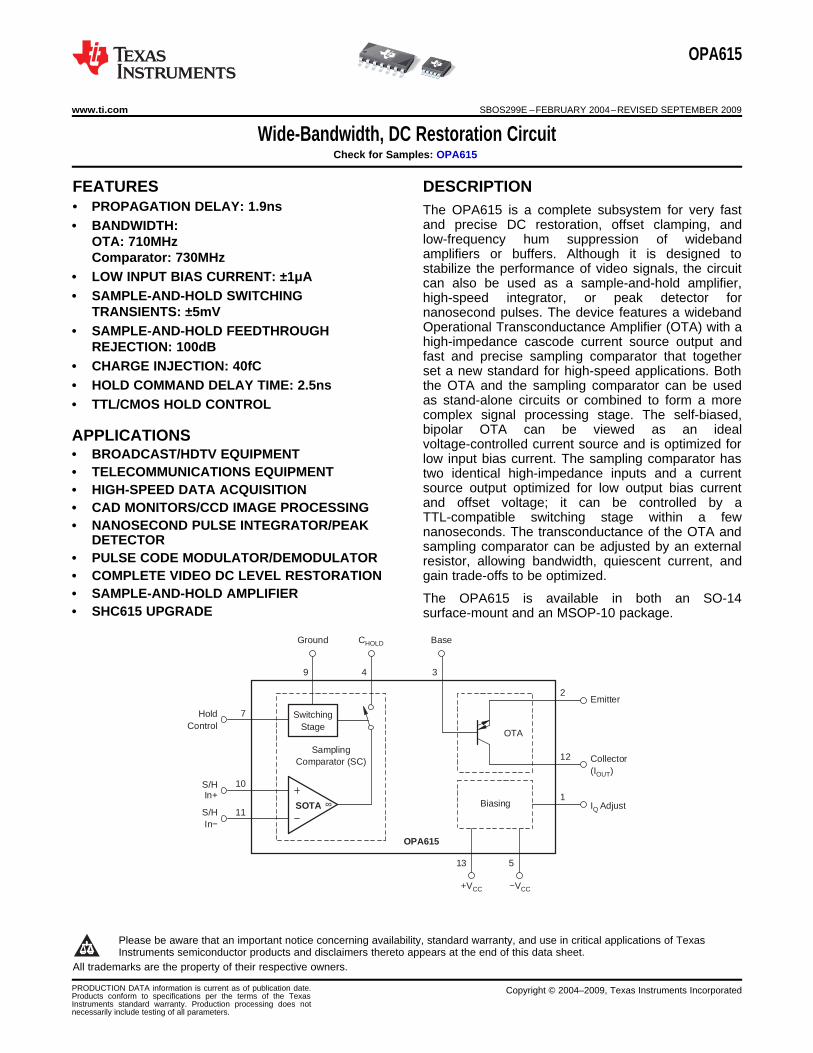
Wide-Bandwidth, DC Restoration CircuitCheck for Samples: OPA615
1FEATURES DESCRIPTION2• PROPAGATION DELAY: 1.9ns The OPA615 is a complete subsystem for very fast
and precise DC restoration, offset clamping, and• BANDWIDTH:low-frequency hum suppression of widebandOTA: 710MHzamplifiers or buffers. Although it is designed toComparator: 730MHzstabilize the performance of video signals, the circuit
• LOW INPUT BIAS CURRENT: ±1μA can also be used as a sample-and-hold amplifier,• SAMPLE-AND-HOLD SWITCHING high-speed integrator, or peak detector for
TRANSIENTS: ±5mV nanosecond pulses. The device features a widebandOperational Transconductance Amplifier (OTA) with a• SAMPLE-AND-HOLD FEEDTHROUGHhigh-impedance cascode current source output andREJECTION: 100dBfast and precise sampling comparator that together
• CHARGE INJECTION: 40fC set a new standard for high-speed applications. Both• HOLD COMMAND DELAY TIME: 2.5ns the OTA and the sampling comparator can be used
as stand-alone circuits or combined to form a more• TTL/CMOS HOLD CONTROLcomplex signal processing stage. The self-biased,bipolar OTA can be viewed as an idealAPPLICATIONSvoltage-controlled current source and is optimized for
• BROADCAST/HDTV EQUIPMENT low input bias current. The sampling comparator has• TELECOMMUNICATIONS EQUIPMENT two identical high-impedance inputs and a current
source output optimized for low output bias current• HIGH-SPEED DATA ACQUISITIONand offset voltage; it can be controlled by a• CAD MONITORS/CCD IMAGE PROCESSINGTTL-compatible switching stage within a few
• NANOSECOND PULSE INTEGRATOR/PEAK nanoseconds. The transconductance of the OTA andDETECTOR sampling comparator can be adjusted by an external
• PULSE CODE MODULATOR/DEMODULATOR resistor, allowing bandwidth, quiescent current, and• COMPLETE VIDEO DC LEVEL RESTORATION gain trade-offs to be optimized.• SAMPLE-AND-HOLD AMPLIFIER The OPA615 is available in both an SO-14• SHC615 UPGRADE surface-mount and an MSOP-10 package.
1
Please be aware that an important notice concerning availability, standard warranty, and use in critical applications of TexasInstruments semiconductor products and disclaimers thereto appears at the end of this data sheet.
2All trademarks are the property of their respective owners.
PRODUCTION DATA information is current as of publication date. Copyright © 2004–2009, Texas Instruments IncorporatedProducts conform to specifications per the terms of the TexasInstruments standard warranty. Production processing does notnecessarily include testing of all parameters.
OPA615
SBOS299E –FEBRUARY 2004–REVISED SEPTEMBER 2009...................................................................................................................................... www.ti.com
This integrated circuit can be damaged by ESD. Texas Instruments recommends that all integrated circuits be handled withappropriate precautions. Failure to observe proper handling and installation procedures can cause damage.
ESD damage can range from subtle performance degradation to complete device failure. Precision integrated circuits may be moresusceptible to damage because very small parametric changes could cause the device not to meet its published specifications.
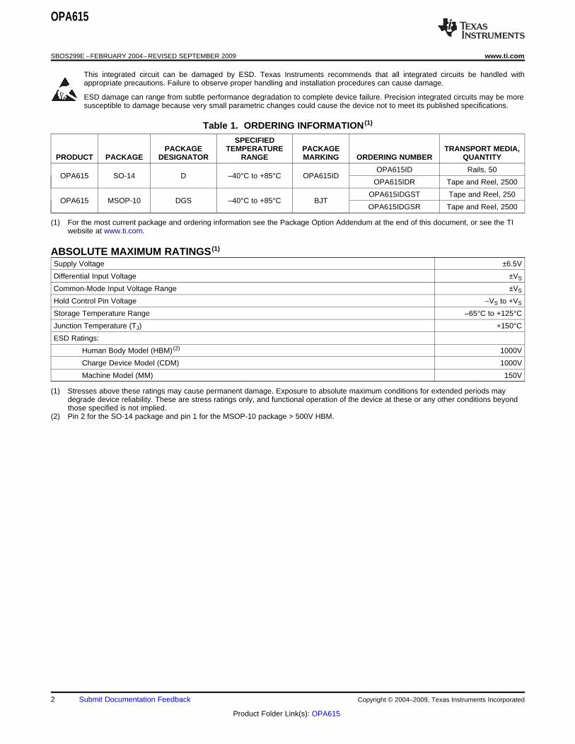
Table 1. ORDERING INFORMATION (1)
SPECIFIEDPACKAGE TEMPERATURE PACKAGE TRANSPORT MEDIA,
PRODUCT PACKAGE DESIGNATOR RANGE MARKING ORDERING NUMBER QUANTITY
OPA615ID Rails, 50OPA615 SO-14 D –40°C to +85°C OPA615ID
OPA615IDR Tape and Reel, 2500
OPA615IDGST Tape and Reel, 250OPA615 MSOP-10 DGS –40°C to +85°C BJT
OPA615IDGSR Tape and Reel, 2500
(1) For the most current package and ordering information see the Package Option Addendum at the end of this document, or see the TIwebsite at www.ti.com.
ABSOLUTE MAXIMUM RATINGS (1)
Supply Voltage ±6.5V
Differential Input Voltage ±VS
Common-Mode Input Voltage Range ±VS
Hold Control Pin Voltage –VS to +VS
Storage Temperature Range –65°C to +125°C
Junction Temperature (TJ) +150°C
ESD Ratings:
Human Body Model (HBM) (2) 1000V
Charge Device Model (CDM) 1000V
Machine Model (MM) 150V
(1) Stresses above these ratings may cause permanent damage. Exposure to absolute maximum conditions for extended periods maydegrade device reliability. These are stress ratings only, and functional operation of the device at these or any other conditions beyondthose specified is not implied.
(2) Pin 2 for the SO-14 package and pin 1 for the MSOP-10 package > 500V HBM.
2 Submit Documentation Feedback Copyright © 2004–2009, Texas Instruments Incorporated
Product Folder Link(s): OPA615
SwitchingStage
SamplingComparator (SC)
OPA615
Biasing
OTA
HoldControl
Emitter2
Collector(IOUT)
12
1S/HIn+
S/HIn−
∞
+VCC −VC C
IQ AdjustSOTA
BaseCHO LDGround
349
7
10
11
13 5
SwitchingStage
SamplingComparator (SC)
OPA615
Biasing
OTA
HoldControl
Emitter1
Collector(IOU T)
9
S/HIn+
S/HIn−
∞
+VCC −VC C
SOTA
BaseCHOLDGround
236
5
7
8
10 4
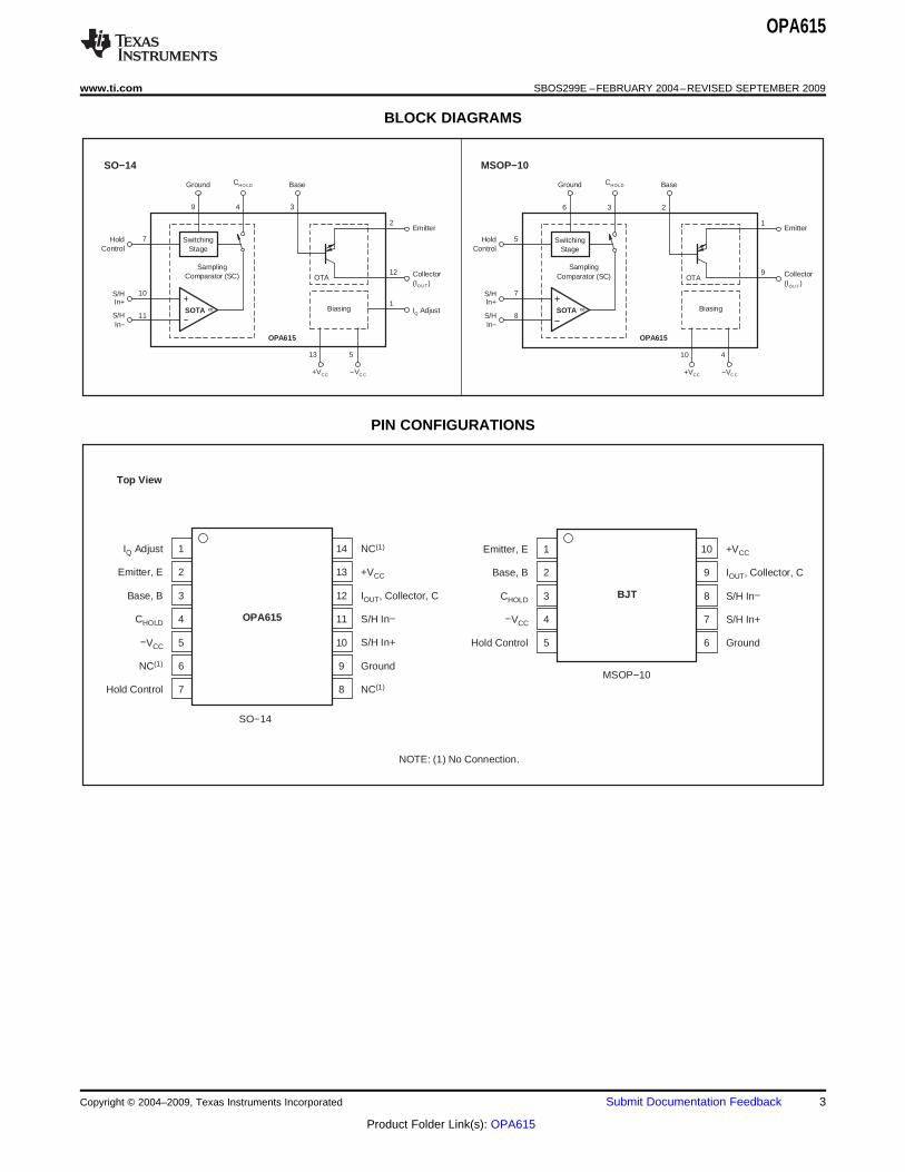
MSOP−10SO−14
1
2
3
4
5
10
9
8
7
6
+VCC
IOUT, Collector, C
S/H In−
S/H In+
Ground
Emitter, E
Base, B
CHOLD
−VCC
Hold Control
BJT
MSOP−10
NOTE: (1) No Connection.
1
2
3
4
5
6
7
14
13
12
11
10
9
8
NC(1)
+VCC
IOUT, Collector, C
S/H In−
S/H In+
Ground
NC(1)
IQ Adjust
Emitter, E
Base, B
CHOLD
−VCC
NC(1)
Hold Control
OPA615
SO−14
Top View
OPA615
www.ti.com...................................................................................................................................... SBOS299E –FEBRUARY 2004–REVISED SEPTEMBER 2009
BLOCK DIAGRAMS
PIN CONFIGURATIONS
Copyright © 2004–2009, Texas Instruments Incorporated Submit Documentation Feedback 3
Product Folder Link(s): OPA615

OPA615
SBOS299E –FEBRUARY 2004–REVISED SEPTEMBER 2009...................................................................................................................................... www.ti.com
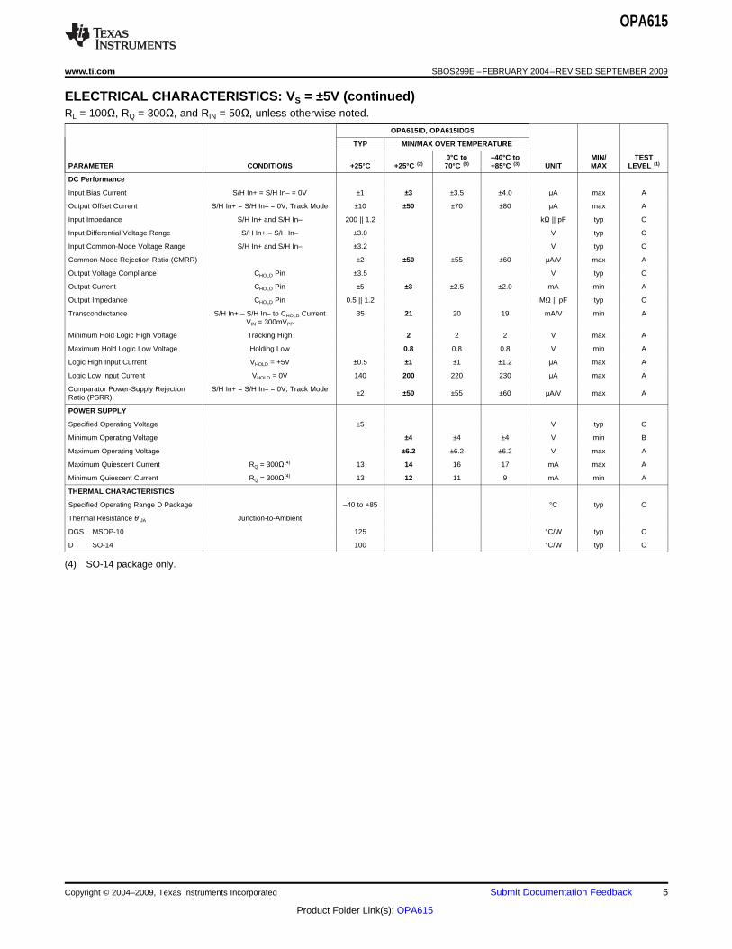
ELECTRICAL CHARACTERISTICS: VS = ±5VRL = 100Ω, RQ = 300Ω, and RIN = 50Ω, unless otherwise noted.
OPA615ID, OPA615IDGS
TYP MIN/MAX OVER TEMPERATURE
0°C to –40°C to MIN/ TESTPARAMETER CONDITIONS +25°C +25°C (2) 70°C (3) +85°C (3) UNIT MAX LEVEL (1)
AC PERFORMANCE (OTA) See Figure 36b
Small-Signal Bandwidth (B to E) VO = 200mVPP, RL = 500Ω 710 MHz min C
VO = 1.4VPP, RL = 500Ω 770 MHz min C
VO = 2.8VPP, RL = 500Ω 230 MHz min C
Large-Signal Bandwidth (B to E) VO = 5VPP, RL = 500Ω 200 MHz min C
Small-Signal Bandwidth (B to C) G = +1, VO = 200mVPP, RL = 100Ω 440 MHz min C
G = +1, VO = 1.4VPP, RL = 100Ω 475 MHz min C
G = +1, VO = 2.8VPP, RL = 100Ω 230 MHz min C
Large-Signal Bandwidth (B to C) G = +1, VO = 5VPP, RL = 100Ω 230 MHz min C
Rise-and-Fall Time (B to E) VO = 2VPP, RL = 500Ω 2 ns max C
Rise-and-Fall Time (B to C) G = +1, VO = 2VPP, RL = 100Ω 2 ns max C
Harmonic Distortion (B to E) RE = 100Ω
2nd-Harmonic VO = 1.4VPP, f = 30MHz –62 –50 –48 –47 dBc min B
3rd-Harmonic VO = 1.4VPP, f = 30MHz –47 –40 –35 –33 dBc min B
Input Voltage Noise Base Input, f > 100kHz 4.6 6.2 6.9 7.4 nV/√Hz max B
Input Current Noise Base Input, f > 100kHz 2.5 3.1 3.6 3.9 pA/√Hz max B
Input Current Noise Emitter Input, f > 100kHz 21 23 25 27 pA/√Hz max B
DC PERFORMANCE (OTA) See Figure 37b
Transconductance (V-base to I-collector) VB = ±5mVPP, RC = 0Ω, RE = 0Ω 72 65 63 58 mA/V min A
B-Input Offset Voltage VB = 0V, RC = 0V, RE = 100Ω ±4 ±40 ±47 ±50 mV max A
B-Input Offset Voltage Drift VB = 0V, RC = 0V, RE = 100Ω ±160 ±160 μV/°C max B
B-Input Bias Current VB = 0V, RC = 0V, RE = 100Ω ±0.5 ±0.9 ±1.5 ±1.7 μA max A
B-Input Bias Current Drift VB = 0V, RC = 0V, RE = 100Ω ±12 ±12 nA/°C max B
E-Input Bias Current VB = 0V, VC = 0V ±35 ±110 ±120 ±135 μA min A
E-Input Bias Current Drift VB = 0V, VC = 0V ±200 ±250 nA/°C max B
C-Output Bias Current VB = 0V, VC = 0V ±35 ±100 ±110 ±125 μA max A
C-Output Bias Current VB = 0V, VC = 0V ±200 ±250 nA/°C max B
INPUT (OTA Base) See Figure 37b
Input Voltage Range RE = 100Ω ±3.4 ±3.2 ±3.1 ±3.0 V min B
Input Impedance B-Input 7 || 1.5 MΩ || pF typ C
OTA Power-Supply Rejection Ratio±VS to VIO at E-Input 54 49 47 46 dB min A
(–PSRR)
OUTPUT (OTA Collector) See Figure 37b
Output Voltage Compliance IE = 2mA ±3.5 ±3.4 ±3.4 ±3.4 V min A
Output Current VC = 0V ±20 ±18 ±17 ±17 mA min A
Output Impedance VC = 0V 1.2 || 2 MΩ || pF typ C
COMPARATOR PERFORMANCE
AC Performance
Output Current Bandwidth IO < 4mAPP 730 520 480 400 MHz min B
Output Current Rise and Fall Time IIO = ±2mAPP, RL = 50Ω at CHOLD 1.4 1.5 1.7 2 ns max B
Control Propagation Delay Time Hold ≥ Track and Track ≥ Hold 2.5 ns typ C
Signal Propagation Delay Time S/H In+ – S/H In– to CHOLD Current 1.9 ns typ C
Input Differential Voltage Noise S/H In+ – S/H In– 6 7.5 8 9 nV/√Hz max B
Charge Injection Track-to-Hold 40 fC typ C
Feedthrough Rejection Hold Mode, VIN = 1VPP, f < 20MHz 100 dB typ C
(1) Test levels: (A) 100% tested at +25°C. Over temperature limits set by characterization and simulation. (B) Limits set by characterizationand simulation. (C) Typical value only for information.
(2) Junction temperature = ambient for +25°C tested specifications.(3) Junction temperature = ambient at low temperature limit; junction temperature = ambient +23°C at high temperature limit for over
temperature specifications.
4 Submit Documentation Feedback Copyright © 2004–2009, Texas Instruments Incorporated
Product Folder Link(s): OPA615
OPA615
www.ti.com...................................................................................................................................... SBOS299E –FEBRUARY 2004–REVISED SEPTEMBER 2009
ELECTRICAL CHARACTERISTICS: VS = ±5V (continued)RL = 100Ω, RQ = 300Ω, and RIN = 50Ω, unless otherwise noted.
OPA615ID, OPA615IDGS
TYP MIN/MAX OVER TEMPERATURE
0°C to –40°C to MIN/ TESTPARAMETER CONDITIONS +25°C +25°C (2) 70°C (3) +85°C (3) UNIT MAX LEVEL (1)
DC Performance
Input Bias Current S/H In+ = S/H In– = 0V ±1 ±3 ±3.5 ±4.0 μA max A
Output Offset Current S/H In+ = S/H In– = 0V, Track Mode ±10 ±50 ±70 ±80 μA max A
Input Impedance S/H In+ and S/H In– 200 || 1.2 kΩ || pF typ C
Input Differential Voltage Range S/H In+ – S/H In– ±3.0 V typ C
Input Common-Mode Voltage Range S/H In+ and S/H In– ±3.2 V typ C
Common-Mode Rejection Ratio (CMRR) ±2 ±50 ±55 ±60 μA/V max A
Output Voltage Compliance CHOLD Pin ±3.5 V typ C
Output Current CHOLD Pin ±5 ±3 ±2.5 ±2.0 mA min A
Output Impedance CHOLD Pin 0.5 || 1.2 MΩ || pF typ C
Transconductance S/H In+ – S/H In– to CHOLD Current 35 21 20 19 mA/V min AVIN = 300mVPP
Minimum Hold Logic High Voltage Tracking High 2 2 2 V max A
Maximum Hold Logic Low Voltage Holding Low 0.8 0.8 0.8 V min A
Logic High Input Current VHOLD = +5V ±0.5 ±1 ±1 ±1.2 μA max A
Logic Low Input Current VHOLD = 0V 140 200 220 230 μA max A
Comparator Power-Supply Rejection S/H In+ = S/H In– = 0V, Track Mode±2 ±50 ±55 ±60 μA/V max A
Ratio (PSRR)
POWER SUPPLY
Specified Operating Voltage ±5 V typ C
Minimum Operating Voltage ±4 ±4 ±4 V min B
Maximum Operating Voltage ±6.2 ±6.2 ±6.2 V max A
Maximum Quiescent Current RQ = 300Ω(4) 13 14 16 17 mA max A
Minimum Quiescent Current RQ = 300Ω(4) 13 12 11 9 mA min A
THERMAL CHARACTERISTICS
Specified Operating Range D Package –40 to +85 °C typ C
Thermal Resistance θ JA Junction-to-Ambient
DGS MSOP-10 125 °C/W typ C
D SO-14 100 °C/W typ C
(4) SO-14 package only.
Copyright © 2004–2009, Texas Instruments Incorporated Submit Documentation Feedback 5
Product Folder Link(s): OPA615
120
100
80
60
40
20
0
Frequency (Hz)
Tra
nsc
ond
uct
anc
e(m
A/V
)
10k 1M 10M 100M 1G
IOUT
VIN
50Ω50Ω
IQ = 14.3mA (89mA/V), RQ = 0Ω
IQ = 13mA (72mA/V), RQ = 300Ω
IQ = 9.6mA (28mA/V), RQ = 2kΩ
VIN = 10mVPP
120
100
80
60
40
30
0
Quiescent Current (mA)
Tra
nsco
ndu
ctan
ce(m
A/V
)
8 9 10 11 12 13 14 15
VIN = 100mVPP
IOUT
VIN
50Ω50Ω
100
90
80
70
60
50
40
30
20
Input Voltage (mV)
Tra
nsco
ndu
ctan
ce(m
A/V
)
−50 −40 −30 −20 −10 0 10 20 30 40 50
Small−Signal Around Input Voltage
IQ = 9.6mA
IQ = 14.3mA
IQ = 13mA
20
15
10
5
0
−5
−10
−15
−20
OTA Input Voltage (mV)
OT
AO
utp
utC
urre
nt(m
A)
−200 0 200−150 −100 −50 50 100 150
IQ = 9.6mA
IQ = 14.3mA
IQ = 13mA
IOUT
VIN
50Ω50Ω
0.15
0.10
0.05
0
−0.05
−0.10
−0.15Time (10ns/div)
Out
put
Vo
ltage
(V)
fIN = 10MHzG = +1V/VVIN = 0.2VPP
3
2
1
0
−1
−2
−3Time (10ns/div)
Out
put
Vo
ltage
(V)
fIN = 10MHzG = +1V/VVIN = 4VPP
OPA615
SBOS299E –FEBRUARY 2004–REVISED SEPTEMBER 2009...................................................................................................................................... www.ti.com
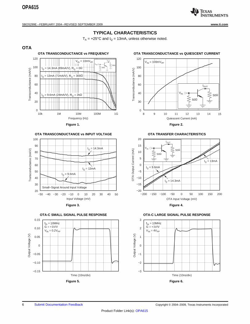
TYPICAL CHARACTERISTICSTA = +25°C and IQ = 13mA, unless otherwise noted.
OTAOTA TRANSCONDUCTANCE vs FREQUENCY OTA TRANSCONDUCTANCE vs QUIESCENT CURRENT
Figure 1. Figure 2.
OTA TRANSCONDUCTANCE vs INPUT VOLTAGE OTA TRANSFER CHARACTERISTICS
Figure 3. Figure 4.
OTA-C SMALL SIGNAL PULSE RESPONSE OTA-C LARGE SIGNAL PULSE RESPONSE
Figure 5. Figure 6.
6 Submit Documentation Feedback Copyright © 2004–2009, Texas Instruments Incorporated
Product Folder Link(s): OPA615
140
120
100
80
60
40
20
0
Quiescent Current (mA)
OT
AB
−In
put
Res
ista
nce
(MΩ
)
8 9 10 1211 13 14 15
18
16
14
12
10
8
6
4
2
0
Quiescent Current (mA)
OT
AC
−O
utpu
tRes
ista
nce
(MΩ
)
8 9 10 11 12 13 14 15
180
160
140
120
100
80
60
40
20
0
Quiescent Current (mA)
OT
AE
−O
utp
utR
esis
tan
ce(Ω
)
8 9 10 11 12 13 14 15
100
10
1
Frequency (Hz)
Vol
tage
Noi
seD
ens
ity(n
V/√
Hz)
Cu
rren
tN
oise
De
nsity
(pA
/√H
z)
100 1k 10k 100k 1M 10M
B−Input Current Noise (2.5pA/√Hz)
B−Input Voltage Noise (4.6nV/√Hz)
E−Input Current Noise (21.0pA/√Hz)
2.0
1.5
1.0
0.5
0
−0.5
−1.0
−1.5
−2.0
Ambient Temperature (C)
B−
Inp
utO
ffse
tVo
ltag
e(m
V)
0.10
0.05
0
−0.05
−0.10
B−
Inp
utB
ias
Cur
rent
(µV
)
−40 −20 1200 20 40 60 80 100
B−Input Bias Current
B−Input Offset Voltage
35302520151050
−5−10−15−20−25−30−35
OTA−B Input Voltage (mV)
OT
A−
CO
utp
utC
urr
ent(
mA
)
−3.5 −3 −2.5 −2 −1.5 −1 −0.5 0 0.5 1 1.5 2 2.5 3 3.5
IO UT
VIN
Degenerated E−InputRE = RL = 100Ω
100Ω
100Ω
IQ = 14.3mA
IQ = 13mA
IQ = 9.6mA
OPA615
www.ti.com...................................................................................................................................... SBOS299E –FEBRUARY 2004–REVISED SEPTEMBER 2009
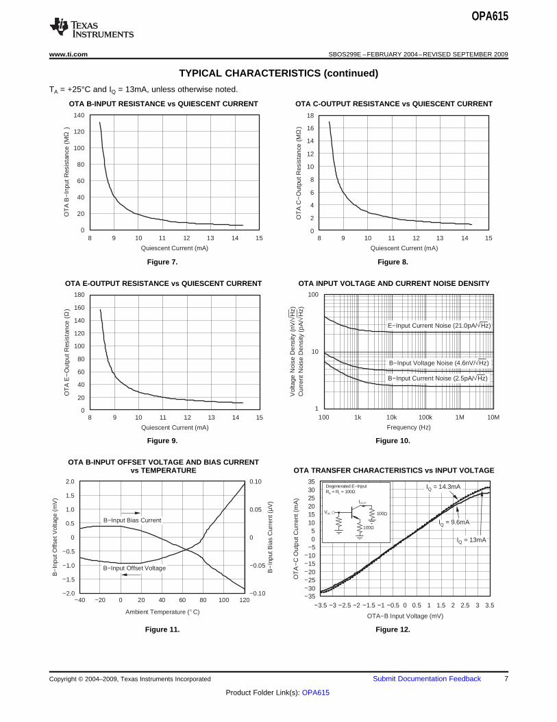
TYPICAL CHARACTERISTICS (continued)
TA = +25°C and IQ = 13mA, unless otherwise noted.
OTA B-INPUT RESISTANCE vs QUIESCENT CURRENT OTA C-OUTPUT RESISTANCE vs QUIESCENT CURRENT
Figure 7. Figure 8.
OTA E-OUTPUT RESISTANCE vs QUIESCENT CURRENT OTA INPUT VOLTAGE AND CURRENT NOISE DENSITY
Figure 9. Figure 10.
OTA B-INPUT OFFSET VOLTAGE AND BIAS CURRENTvs TEMPERATURE OTA TRANSFER CHARACTERISTICS vs INPUT VOLTAGE
Figure 11. Figure 12.
Copyright © 2004–2009, Texas Instruments Incorporated Submit Documentation Feedback 7
Product Folder Link(s): OPA615
200
160
120
80
40
0
−40
−80
−120
−160
−200Time (20ns/div)
Ou
tput
Vol
tage
(mV
)
2.0
1.6
1.2
0.8
0.4
0
−0.4
−0.8
−1.2
−1.6
−2.0
Out
put
Vol
tage
(V)
VIN
VO50Ω
100Ω
500Ω
Small−Signal±80mVLeft Scale
Large−Signal±1.6V
Right Scale
3
0
−3
−6
−9
−12
−15
Frequency (Hz)
Ga
in(d
B)
1M 10M 100M 1G
VIN
VO50Ω
100Ω
500Ω
VO = 0.6VPP
VO = 1.4VPP
VO = 5VPP
VO = 2.8VPP
VO = 0.2VPP
−40
−45
−50
−55
−60
−65
−70
Frequency (MHz)
Ha
rmon
icD
isto
rtio
n(d
Bc)
1 10 100
VOUT = 1.4VPP
2nd−Harmonic
3rd−Harmonic
VIN
VOUT50Ω
100Ω
3
0
−3
−6
−9
−12
−15
Frequency (Hz)
Gai
n(d
B)
1M 10M 100M 1G
VO = 0.6VPP
VO = 1.4VPP
VO = 0.2VPP
VO = 2.8VPP
VO = 5VPP
VIN
VO
50Ω
100Ω
100Ω
−20
−25
−30
−35
−40
−45
−50
−55
−60
Frequency (MHz)
Har
mon
icD
isto
rtio
n(d
Bc)
1 10 100
VOUT = 1.4VPPVOU T
VIN
50Ω100Ω
100Ω
3rd−Harmonic
2nd−Harmonic
16
15
14
13
12
11
10
9
8
Qui
esc
ent
Cur
rent
(mA
)
0.1 1 10 100 1k 10k 100k
RQ (Ω)
+IQ
−IQ
OPA615
SBOS299E –FEBRUARY 2004–REVISED SEPTEMBER 2009...................................................................................................................................... www.ti.com
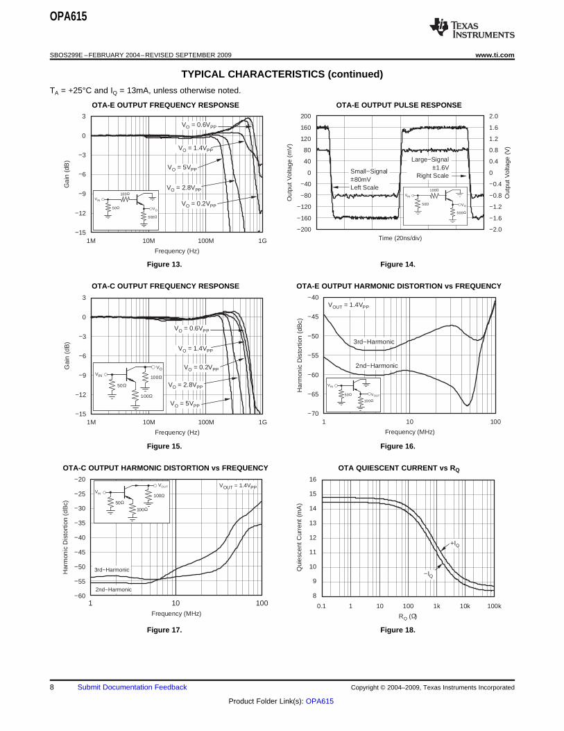
TYPICAL CHARACTERISTICS (continued)
TA = +25°C and IQ = 13mA, unless otherwise noted.
OTA-E OUTPUT FREQUENCY RESPONSE OTA-E OUTPUT PULSE RESPONSE
Figure 13. Figure 14.
OTA-C OUTPUT FREQUENCY RESPONSE OTA-E OUTPUT HARMONIC DISTORTION vs FREQUENCY
Figure 15. Figure 16.
OTA-C OUTPUT HARMONIC DISTORTION vs FREQUENCY OTA QUIESCENT CURRENT vs RQ
Figure 17. Figure 18.
8 Submit Documentation Feedback Copyright © 2004–2009, Texas Instruments Incorporated
Product Folder Link(s): OPA615
40
30
20
10
0
Frequency (Hz)
Tra
nsco
nduc
tanc
e(m
A/V
)
1M 10M 100M 1G
VIN
50Ω
IO UT
+5V
SOTA
Hold Control
50Ω
∞
VIN = 10mVPP
40
30
20
10
0
Quiescent Current (mA)
Tra
nsc
ond
ucta
nce
(mA
/V)
8 9 10 11 12 13 14 15
RQ Adjusted
45
40
35
30
25
20
15
10
5
0
Input Voltage (mV)
Tra
nsc
ondu
ctan
ce(m
A/V
)
−100 −80 −60 −40 −20 0 20 40 60 80 100
Small−Signal Around Input Voltage
8
6
4
2
0
−2
−4
−6
−8
SOTA Input Voltage (mV)
SO
TA
Out
putC
urre
nt(m
A)
−200 −150 −100 −50 0 50 100 150 200
150
100
50
0
−50
−100
−150Time (10ns/div)
Ou
tput
Vol
tage
(mV
)
fIN = 20MHzRL = 50ΩIOUT = 4mAPPtRISE = 2ns
Hold Control = +5V
150
100
50
0
−50
−100
−150Time (10ns/div)
Ou
tput
Vol
tage
(mV
)
fIN = 20MHzRL = 50ΩIOUT = 4mAPPtRISE = 10ns
Hold Control = +5V
OPA615
www.ti.com...................................................................................................................................... SBOS299E –FEBRUARY 2004–REVISED SEPTEMBER 2009
TYPICAL CHARACTERISTICS (continued)
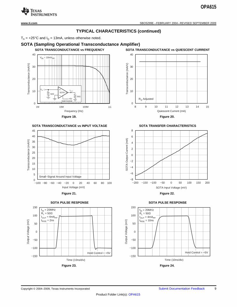
TA = +25°C and IQ = 13mA, unless otherwise noted.
SOTA (Sampling Operational Transconductance Amplifier)SOTA TRANSCONDUCTANCE vs FREQUENCY SOTA TRANSCONDUCTANCE vs QUIESCENT CURRENT
Figure 19. Figure 20.
SOTA TRANSCONDUCTANCE vs INPUT VOLTAGE SOTA TRANSFER CHARACTERISTICS
Figure 21. Figure 22.
SOTA PULSE RESPONSE SOTA PULSE RESPONSE
Figure 23. Figure 24.
Copyright © 2004–2009, Texas Instruments Incorporated Submit Documentation Feedback 9
Product Folder Link(s): OPA615
1.3
1.2
1.1
1.0
0.9
0.8
Input Voltage (mV)
Pro
pagation D
ela
y (
ns)
0 400 600200 800 1000 1200
Negative
Positive
VOD
100W
100W
VOD
GNDSOTA
VOD
2.0
1.8
1.6
1.4
1.2
1.0
0.8
0.6
0.4
0.2
0
Temperature (C)
Pro
paga
tion
Del
ay(n
s)
−40 −20 1200 20 40 60 80 100
Falling Edge
Rising Edge
10
5
0
−5
−10Time (10ns/div)
Sw
itchi
ng
Tra
nsi
ent(
mV
)100Ω
100Ω
TTL
50Ω
VOUT
ON −OFF
OFF −ON
1.4
1.3
1.2
1.1
1.0
0.9
0.8
Rise Time (ns)
Pro
paga
tion
Del
ay(n
s)
0 3 4 51 2 6 7 8 9 10
Positive
Negative
VIN = 1.2Vpp
−0.6V
+0.6V
0V
150
100
50
0
−50
−100
−150Time (10ns/div)
Out
put
Vo
ltage
(mV
)
2.5
2.0
1.5
1.0
0.5
0
−50
Ho
ldC
omm
and
(V) 6
3
0
−3
−6
−9
−12
−15
Frequency (Hz)
Gai
n(d
B)
1M 10M 100M 2G1G
IOUT = 0.5mAPP
IOUT = 4mAPP
IOUT = 2mAPP
OPA615
SBOS299E –FEBRUARY 2004–REVISED SEPTEMBER 2009...................................................................................................................................... www.ti.com
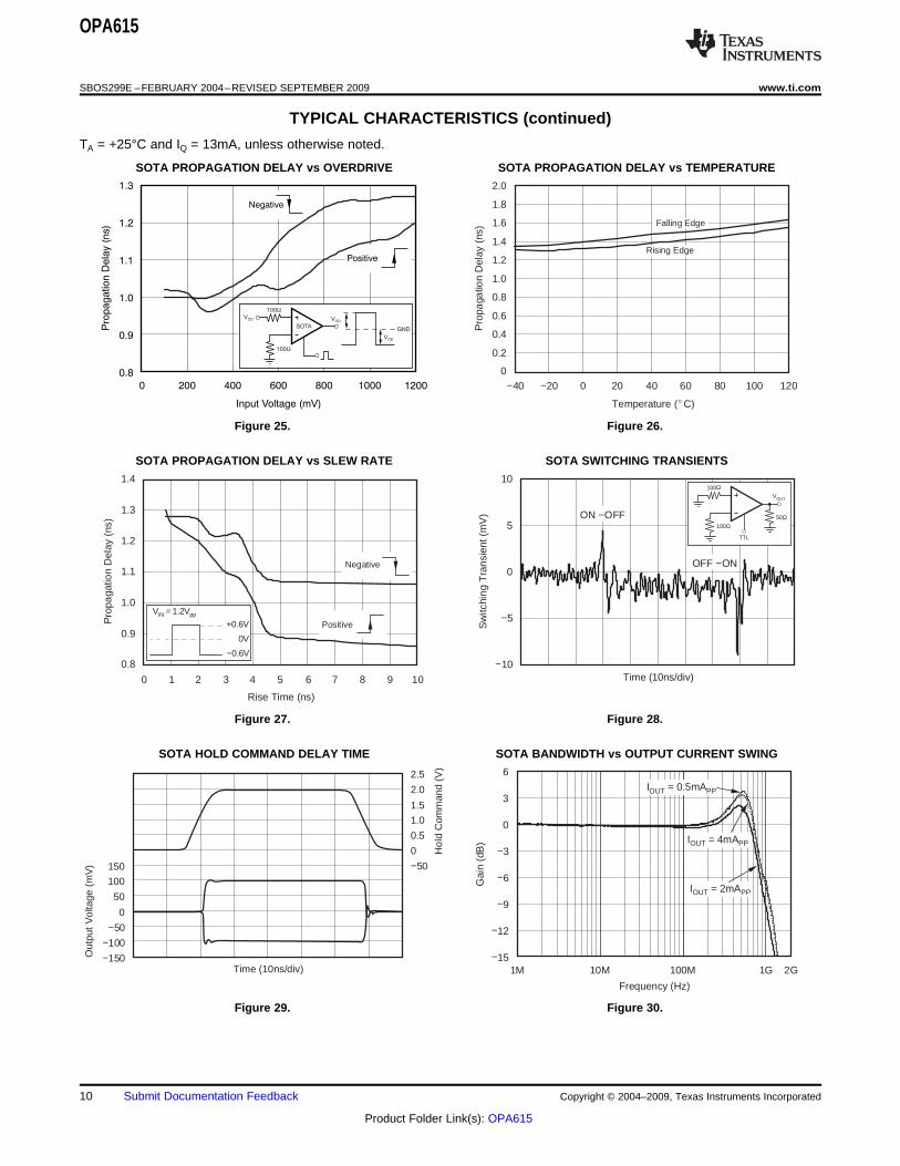
TYPICAL CHARACTERISTICS (continued)
TA = +25°C and IQ = 13mA, unless otherwise noted.
SOTA PROPAGATION DELAY vs OVERDRIVE SOTA PROPAGATION DELAY vs TEMPERATURE
Figure 25. Figure 26.
SOTA PROPAGATION DELAY vs SLEW RATE SOTA SWITCHING TRANSIENTS
Figure 27. Figure 28.
SOTA HOLD COMMAND DELAY TIME SOTA BANDWIDTH vs OUTPUT CURRENT SWING
Figure 29. Figure 30.
10 Submit Documentation Feedback Copyright © 2004–2009, Texas Instruments Incorporated
Product Folder Link(s): OPA615
0
−20
−40
−60
−80
−100
−120
Frequency (Hz)
Fee
dthr
oug
hR
ejec
tion
(dB
)
1M 10M 100M 1G
Hold Control = 0V(Off−Isolation)
0
−20
−40
−60
−80
−100
−120
Frequency (Hz)
Com
mo
n−M
ode
Rej
ectio
n(d
B)
100k 1M 10M 1G100M
Hold Control = 5VV+ = V−
50
40
30
20
10
0
−10
−20
−30
−40
−50
Temperature (C)
Out
putB
ias
Cur
rent
(µA
)
−40 −20 1200 20 40 60 80 100
Hold Control = 5VV+ = V− = 0V
0.40
0.35
0.30
0.25
0.20
0.15
0.10
0.05
0
Temperature (C)
Inp
utB
ias
Cur
rent
(µA
)
−40 −20 1200 20 40 60 80 100
Positive Input
Negative Input
OPA615
www.ti.com...................................................................................................................................... SBOS299E –FEBRUARY 2004–REVISED SEPTEMBER 2009
TYPICAL CHARACTERISTICS (continued)
TA = +25°C and IQ = 13mA, unless otherwise noted.
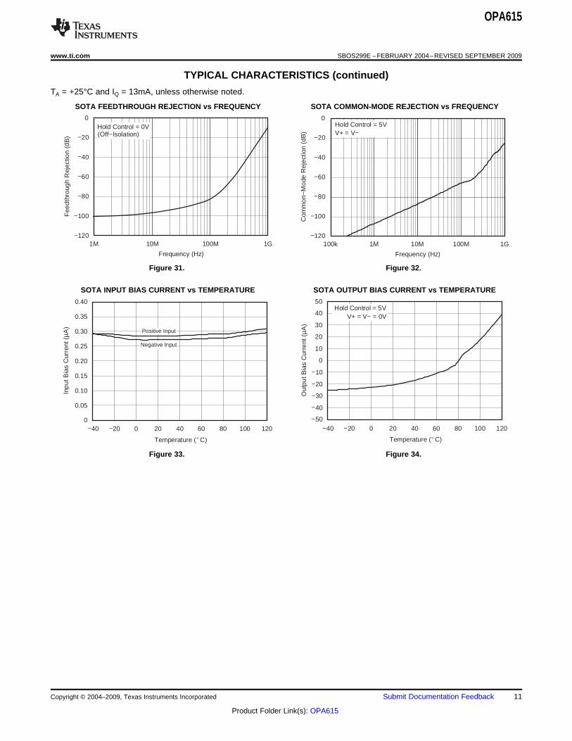
SOTA FEEDTHROUGH REJECTION vs FREQUENCY SOTA COMMON-MODE REJECTION vs FREQUENCY
Figure 31. Figure 32.
SOTA INPUT BIAS CURRENT vs TEMPERATURE SOTA OUTPUT BIAS CURRENT vs TEMPERATURE
Figure 33. Figure 34.
Copyright © 2004–2009, Texas Instruments Incorporated Submit Documentation Feedback 11
Product Folder Link(s): OPA615

IC VIN
rE REor RE
VIN
IC rE
OPA615
SBOS299E –FEBRUARY 2004–REVISED SEPTEMBER 2009...................................................................................................................................... www.ti.com
DISCUSSION OF PERFORMANCE
The OPA615, which contains a wideband Operational OPERATIONAL TRANSCONDUCTANCETransconductance Amplifier (OTA) and a fast AMPLIFIER (OTA) SECTIONsampling comparator (SOTA), represents a completesubsystem for very fast and precise DC restoration,
OVERVIEWoffset clamping and correction to GND or to anadjustable reference voltage, and low frequency hum The symbol for the OTA section is similar to that of asuppression of wideband operational or buffer bipolar transistor, and the self-biased OTA can beamplifiers. viewed as either a quasi-ideal transistor or as a
voltage-controlled current source. Application circuitsAlthough the IC was designed to improve or stabilizefor the OTA look and operate much like transistorthe performance of complex, wideband video signals,circuits—the bipolar transistor is also ait can also be used as a sample-and-hold amplifier,voltage-controlled current source. Like a transistor, ithigh-speed integrator, peak detector for nanosecondhas three terminals: a high-impedance input (base)pulses, or as part of a correlated double samplingoptimized for a low input bias current of 0.3μA, asystem. A wideband Operational Transconductancelow-impedance input/output (emitter), and theAmplifier (OTA) with a high-impedance cascodehigh-impedance current output (collector).current source output and a fast and precise
sampling comparator sets a new standard for The OTA consists of a complementary bufferhigh-speed sampling applications. amplifier and a subsequent complementary current
mirror. The buffer amplifier features a DarlingtonBoth the OTA and the sampling comparator can beoutput stage and the current mirror has a cascodedused as stand-alone circuits or combined to createoutput. The addition of this cascode circuitrymore complex signal processing stages such asincreases the current source output resistance tosample-and-hold amplifiers. The OPA615 simplifies1.2MΩ. This feature improves the OTA linearity andthe design of input amplifiers with high humdrive capabilities. Any bipolar input voltage at thesuppression; clamping or DC-restoration stages inhigh impedance base has the same polarity andprofessional broadcast equipment, high-resolutionsignal level at the low impedance buffer or emitterCAD monitors and information terminals; and signaloutput. For the open-loop diagrams, the emitter isprocessing stages for the energy and peak value ofconnected to GND; the collector current is thennanoseconds pulses. This device also eases thedetermined by the voltage between base and emitterdesign of high-speed data acquisition systems behindtimes the transconductance. In application circuitsa CCD sensor or in front of an analog-to-digital(Figure 36b), a resistor RE between the emitter andconverter (ADC).GND is used to set the OTA transfer characteristics.
An external resistor on the SO-14 package, RQ,The following formulas describe the most importantallows the user to set the quiescent current. RQ isrelationships. re is the output impedance of the bufferconnected from Pin 1 (IQ adjust) to –VCC. Itamplifier (emitter) or the reciprocal of the OTAdetermines the operating currents of the OTA sectiontransconductance. Above ±5mA, the collector current,and controls the bandwidth and AC behavior as wellIC, will be slightly less than indicated by the formula.as the transconductance of the OTA.
Besides the quiescent current setting feature, a(1)Proportional-to-Absolute-Temperature (PTAT) supply
current control will increase the quiescent current The RE resistor may be bypassed by a relatively largeversus temperature. This variation holds the capacitor to maintain high AC gain. The paralleltransconductance (gm) of the OTA and comparator combination of RE and this large capacitor form arelatively constant versus temperature. The circuit high-pass filter, enhancing the high frequency gain.parameters listed in the specification table are Other cases may require an RC compensationmeasured with RQ set to 300Ω, giving a nominal network in parallel to RE to optimize thequiescent current at 13mA. While not always shown high-frequency response. The large-signal bandwidthin the application circuits, this RQ = 300Ω is required (VO = 1.4VPP) measured at the emitter achievesto get the 13mA quiescent operating current. 770MHz. The frequency response of the collector is
directly related to the resistor value between thecollector and GND; it decreases with increasingresistor values, because of the low-pass filter formedwith the OTA C-output capacitance.
12 Submit Documentation Feedback Copyright © 2004–2009, Texas Instruments Incorporated
Product Folder Link(s): OPA615
+VCC(13)
+VCC(5)
C(12)
B(3)
E(2)
+1
RB RL
RB RE
V−Single Transistor
V+
VI
VO
(a) Common Emitter Amplifier
VO
100ΩOTAVI
B
ERL
RE
NoninvertingGain
(b) Common−E Amplifier for OTA
Inverting GainV several voltsOS ≈
3
2
C12
Transconductance varies over temperature. Transconductance remains constant over temperature.
VOS ≈ 0
OPA615
www.ti.com...................................................................................................................................... SBOS299E –FEBRUARY 2004–REVISED SEPTEMBER 2009
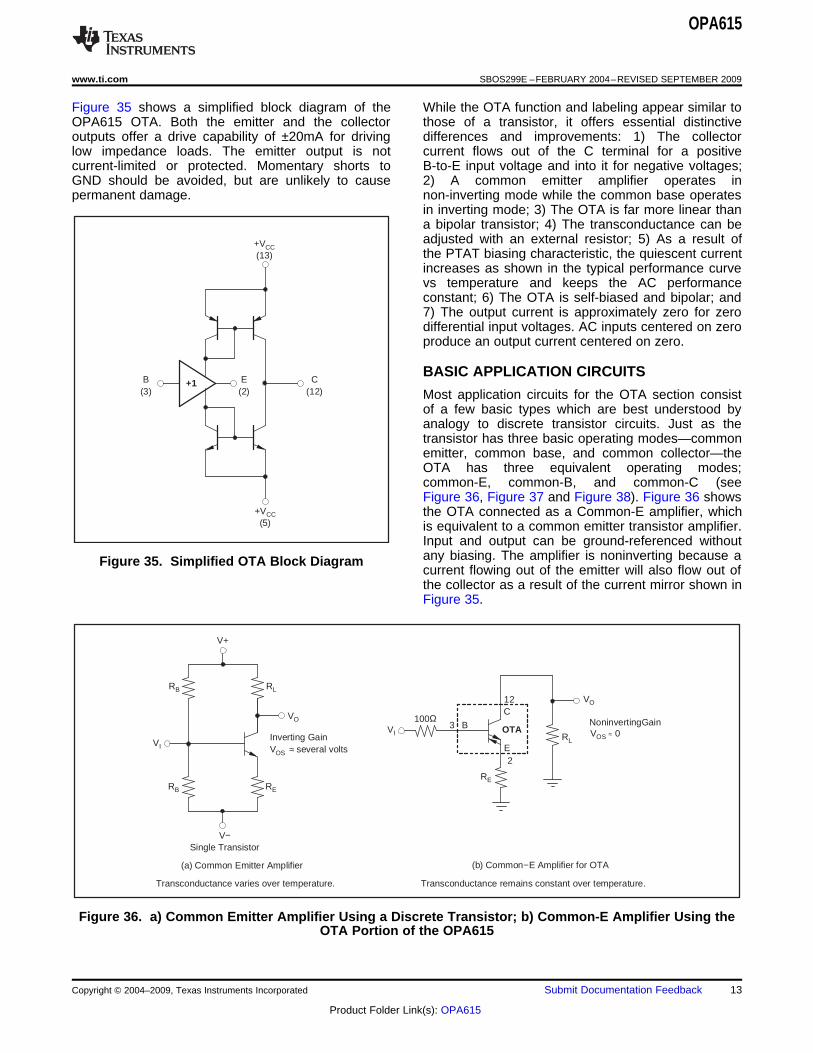
Figure 35 shows a simplified block diagram of the While the OTA function and labeling appear similar toOPA615 OTA. Both the emitter and the collector those of a transistor, it offers essential distinctiveoutputs offer a drive capability of ±20mA for driving differences and improvements: 1) The collectorlow impedance loads. The emitter output is not current flows out of the C terminal for a positivecurrent-limited or protected. Momentary shorts to B-to-E input voltage and into it for negative voltages;GND should be avoided, but are unlikely to cause 2) A common emitter amplifier operates inpermanent damage. non-inverting mode while the common base operates
in inverting mode; 3) The OTA is far more linear thana bipolar transistor; 4) The transconductance can beadjusted with an external resistor; 5) As a result ofthe PTAT biasing characteristic, the quiescent currentincreases as shown in the typical performance curvevs temperature and keeps the AC performanceconstant; 6) The OTA is self-biased and bipolar; and7) The output current is approximately zero for zerodifferential input voltages. AC inputs centered on zeroproduce an output current centered on zero.
BASIC APPLICATION CIRCUITS
Most application circuits for the OTA section consistof a few basic types which are best understood byanalogy to discrete transistor circuits. Just as thetransistor has three basic operating modes—commonemitter, common base, and common collector—theOTA has three equivalent operating modes;common-E, common-B, and common-C (seeFigure 36, Figure 37 and Figure 38). Figure 36 showsthe OTA connected as a Common-E amplifier, whichis equivalent to a common emitter transistor amplifier.Input and output can be ground-referenced withoutany biasing. The amplifier is noninverting because aFigure 35. Simplified OTA Block Diagramcurrent flowing out of the emitter will also flow out ofthe collector as a result of the current mirror shown inFigure 35.
Figure 36. a) Common Emitter Amplifier Using a Discrete Transistor; b) Common-E Amplifier Using theOTA Portion of the OPA615
Copyright © 2004–2009, Texas Instruments Incorporated Submit Documentation Feedback 13
Product Folder Link(s): OPA615
V−Single Transistor
V+
VI
VO
(a) Common Collector Amplifier(Emitter Follower)
VO
100ΩOTAVI
(b) Common−C Amplifier for OTA(Buffer)
≈OS
G 1V 0.7V≈
≈OS
G 1V 0≈
B3C12
RE
RE
RO = 1gm
G = ≈ 11 + 1
gm x RE
1
E2
Inverting Gain
VI
VO
Single Transistor(a) Common−Base
Amplifier
OTA
VI
(b) Common−B Amplifier for OTA
OS
RL
Noninverting GainV several volts
RE
VO
RL
RE
≈
B
E
3
2
C12
G = − ≈ −RL
RE +gm
1
RL
RE
VOS ≈ 0
V+
100Ω
OPA615
SBOS299E –FEBRUARY 2004–REVISED SEPTEMBER 2009...................................................................................................................................... www.ti.com
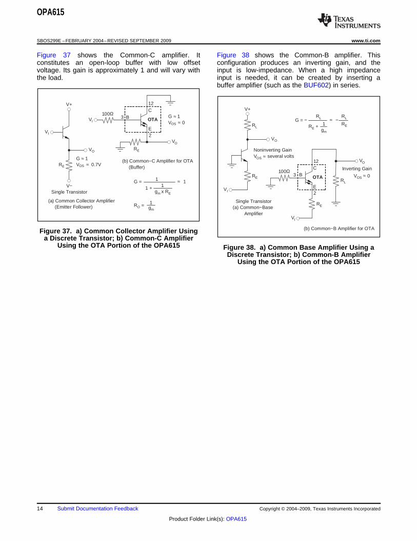
Figure 37 shows the Common-C amplifier. It Figure 38 shows the Common-B amplifier. Thisconstitutes an open-loop buffer with low offset configuration produces an inverting gain, and thevoltage. Its gain is approximately 1 and will vary with input is low-impedance. When a high impedancethe load. input is needed, it can be created by inserting a
buffer amplifier (such as the BUF602) in series.
Figure 37. a) Common Collector Amplifier Usinga Discrete Transistor; b) Common-C Amplifier
Using the OTA Portion of the OPA615 Figure 38. a) Common Base Amplifier Using aDiscrete Transistor; b) Common-B Amplifier
Using the OTA Portion of the OPA615
14 Submit Documentation Feedback Copyright © 2004–2009, Texas Instruments Incorporated
Product Folder Link(s): OPA615
Offset (V) Charge (pC)CHTotal (pF)
OPA615
www.ti.com...................................................................................................................................... SBOS299E –FEBRUARY 2004–REVISED SEPTEMBER 2009
SAMPLING COMPARATOR The additional offset voltage or switching transientinduced on a capacitor at the current source output
The OPA615 sampling comparator features a very by the switching charge can be determined by theshort switching (2.5ns) propagation delay and utilizes following formula:a new switching circuit architecture to achieveexcellent speed and precision.
(2)It provides high impedance inverting and noninvertinganalog inputs, a high-impedance current source The switching stage input is insensitive to the lowoutput and a TTL-CMOS-compatible Hold Control slew rate performance of the hold control commandInput. and compatible with TTL/CMOS logic levels. With
TTL logic high, the comparator is active, comparingThe sampling comparator consists of an operational the two input voltages and varying the output currenttransconductance amplifier (OTA), a buffer amplifier, accordingly. With TTL logic low, the comparatorand a subsequent switching circuit. This combination output is switched off, showing a very highis subsequently referred to as the Sampling impedance to the hold capacitor.Operational Transconductance Amplifier (SOTA). TheOTA and buffer amplifier are directly tied together at DESIGN-IN TOOLSthe buffer outputs to provide the two identicalhigh-impedance inputs and high open-loop
Demonstration Fixturetransconductance. Even a small differential inputvoltage multiplied with the high transconductance Two printed circuit boards (PCBs) are available toresults in an output current—positive or assist in the initial evaluation of circuit performancenegative—depending upon the input polarity. This using the OPA615. The demonstration fixture ischaracteristic is similar to the low or high status of a offered free of charge as an unpopulated PCB,conventional comparator. The current source output delivered with a user's guide. The summaryfeatures high output impedance, output bias current information for this fixture is shown in Table 2.compensation, and is optimized for charging acapacitor in DC restoration, nanosecond integrators, Table 2. OPA615 Demonstration Fixturespeak detectors and S/H circuits. The typical
ORDERING LITERATUREcomparator output current is ±5mA and the outputPRODUCT PACKAGE NUMBER NUMBERbias current is minimized to typically ±10μA in theOPA615ID SO-14 DEM-OPA-SO-1C SBOU039sampling mode.
OPA615IDGS MSOP-10 DEM-OPA-MSOP-1A SBOU042This innovative circuit achieves the high slew raterepresentative of an open-loop design. In addition, The demonstration fixture can be requested at thethe acquisition slew current for a hold or storage Texas Instruments web site (www.ti.com) through thecapacitor is higher than standard diode bridge and OPA615 product folder.switch configurations, removing a main contributor tothe limits of maximum sampling rate and input Macromodel and Applications Supportfrequency.
Computer simulation of circuit performance usingThe switching circuits in the OPA615 use current SPICE is often a quick way to analyze thesteering (versus voltage switching) to provide performance of analog circuits and systems. This isimproved isolation between the switch and analog particularly true for video and RF amplifier circuitssections. This design results in low aperture time where parasitic capacitance and inductance can havesensitivity to the analog input signal, reduced power a major effect on circuit performance. A SPICE modelsupply and analog switching noise. Sample-to-hold for the OPA615 is available through the TI web pagepeak switching charge injection is 40fC. (www.ti.com). This model predicts typical small-signal
AC, transient steps, DC performance, and noiseunder a wide variety of operating conditions. Themodel includes the noise terms found in the electricalspecifications of the data sheet. However, the modeldoes not attempt to distinguish between packagetypes in their small-signal AC performance. Theapplications department is also available for designassistance.
Copyright © 2004–2009, Texas Instruments Incorporated Submit Documentation Feedback 15
Product Folder Link(s): OPA615
SOTA
OTA
RQRQ
GND9 34
Switching Stage
Sampling Comparator(SC)
7
10
11
S/H In+
S/H In−
HoldControl
CHOLD
Base
RB(25Ω to 200Ω)
2
12
Biasing
513−VCC+VCC−5V+5V
1
2.2µF 10nF 470pF 10nF 2.2µF470pF
Solid Tantalum
+
+
RQ
IQ Adjust
Collector
Emitter
RQ = 300Ωsets approximatelyIQ = 13mA
(20Ωto
200Ω)
∞
OPA615
SBOS299E –FEBRUARY 2004–REVISED SEPTEMBER 2009...................................................................................................................................... www.ti.com
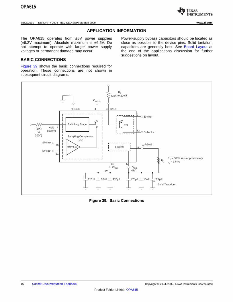
APPLICATION INFORMATION
The OPA615 operates from ±5V power supplies Power-supply bypass capacitors should be located as(±6.2V maximum). Absolute maximum is ±6.5V. Do close as possible to the device pins. Solid tantalumnot attempt to operate with larger power supply capacitors are generally best. See Board Layout atvoltages or permanent damage may occur. the end of the applications discussion for further
suggestions on layout.BASIC CONNECTIONS
Figure 39 shows the basic connections required foroperation. These connections are not shown insubsequent circuit diagrams.
Figure 39. Basic Connections
16 Submit Documentation Feedback Copyright © 2004–2009, Texas Instruments Incorporated
Product Folder Link(s): OPA615
HCL
VIN
CHOLD
VOUT
OTA
OPA615
10
11
7
4
2
3
12100Ω
100Ω
SOTA
100Ω
SOTA
HCL
VIN
CHOLD
VOUT
OTA
R1 R2
R2
R1
= VIN x
OPA615
3
12
2
47 10
11
100Ω
100Ω
100Ω
G R2
R1
7.5
BLANKING
BACK PORCH
100 89 70 59 41 30 11 0
W Y CY GRN MAG R BLU BLK
FRONT PORCH
SYNC TIP
BREEZEWAY
COLOR BURST
LUMINANCE + CHROMINANCE
100
80
60
40
2010
0
−20
−40
IRE
UN
ITS
40
IRE
1VP
P
OPA615
www.ti.com...................................................................................................................................... SBOS299E –FEBRUARY 2004–REVISED SEPTEMBER 2009
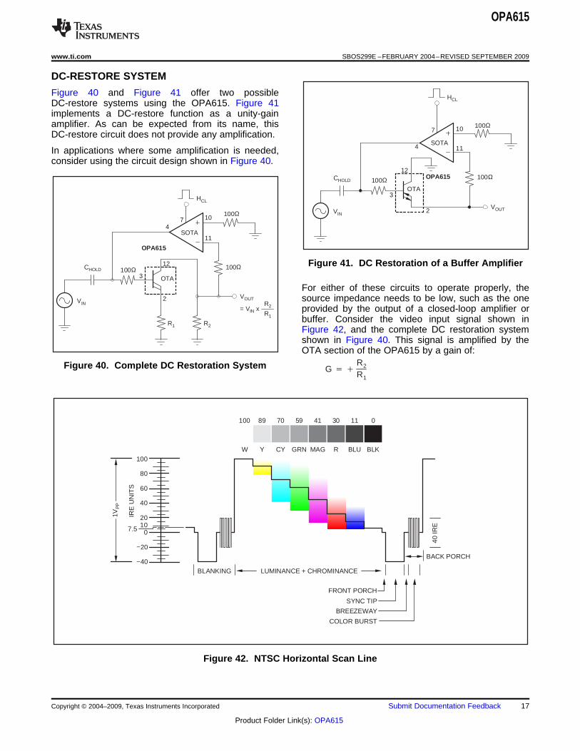
DC-RESTORE SYSTEM
Figure 40 and Figure 41 offer two possibleDC-restore systems using the OPA615. Figure 41implements a DC-restore function as a unity-gainamplifier. As can be expected from its name, thisDC-restore circuit does not provide any amplification.
In applications where some amplification is needed,consider using the circuit design shown in Figure 40.
Figure 41. DC Restoration of a Buffer Amplifier
For either of these circuits to operate properly, thesource impedance needs to be low, such as the oneprovided by the output of a closed-loop amplifier orbuffer. Consider the video input signal shown inFigure 42, and the complete DC restoration systemshown in Figure 40. This signal is amplified by theOTA section of the OPA615 by a gain of:
Figure 40. Complete DC Restoration System
Figure 42. NTSC Horizontal Scan Line
Copyright © 2004–2009, Texas Instruments Incorporated Submit Documentation Feedback 17
Product Folder Link(s): OPA615
Sample
0V
7.5
100
80
60
40
2010
0
−20
−40
0V
Hold
HC
L
Out
putV
olta
geIn
putV
olta
ge
IRE
UN
ITS
7.5
100
80
60
40
2010
0
−20
−40
IRE
UN
ITS
OPA615
SBOS299E –FEBRUARY 2004–REVISED SEPTEMBER 2009...................................................................................................................................... www.ti.com
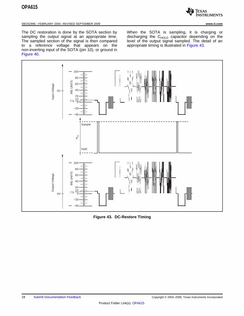
The DC restoration is done by the SOTA section by When the SOTA is sampling, it is charging orsampling the output signal at an appropriate time. discharging the CHOLD capacitor depending on theThe sampled section of the signal is then compared level of the output signal sampled. The detail of anto a reference voltage that appears on the appropriate timing is illustrated in Figure 43.non-inverting input of the SOTA (pin 10), or ground inFigure 40.
Figure 43. DC-Restore Timing
18 Submit Documentation Feedback Copyright © 2004–2009, Texas Instruments Incorporated
Product Folder Link(s): OPA615

OPA656
R2
300Ω
RE
OTA
VIN RB
VOUT
HCL
CHOLD
• Current Control
• Non−Inverting
OPA615
100Ω
2
34
7
11
10
12
100ΩVREF
100Ω
R1
300Ω
SOTA
CB
Hold /Track
50Ω
100Ω
150Ω100Ω
OTA
2
12
34
300Ω
50ΩCHOLD22pF
VIN
10
11
7
300Ω
VOUT
SOTA
OPA615
+2.5
+1.5
+0.5
−0.5
−1.5
−2.5
1MHz SAMPLE−AND−HOLD OF A 100kHz SINEWAVE
Time (1µs/div)
Ou
tput
Vo
ltag
e(V
)
5
4
3
2
1
0
Ho
ld−
an
d−
Tra
ckS
ign
al(
V)
OPA615
www.ti.com...................................................................................................................................... SBOS299E –FEBRUARY 2004–REVISED SEPTEMBER 2009
CLAMPED VIDEO/RF AMPLIFIER The external capacitor (CHOLD) allows for a widerange of flexibility. By choosing small values, theAnother circuit example for the preamplifier and thecircuit can be optimized for a short clamping period orclamp circuit is shown in Figure 44. The preamplifierwith high values for a low droop rate. Anotheruses the wideband, low noise OPA656, againadvantage of this circuit is that small clamp peaks atconfigured in a gain of +2V/V. Here, the OPA656 hasthe output of the switching comparator are integrateda typical bandwidth of 200MHz with a settling time ofand do not cause glitches in the signal path.about 21ns (0.02%) and offers a low bias current
JFET input stage.SAMPLE-AND-HOLD AMPLIFIER
With a control propagation delay of 2.5ns and730MHz bandwidth, the OPA615 can be usedadvantageously in a high-speed sample-and-holdamplifier. Figure 45 illustrates this configuration.
Figure 44. Clamped Video/RF Amplifier Figure 45. Sample-and-Hold Amplifier
The video signal passes through the capacitor CB, To illustrate how the digitization is realized in theblocking the DC component. To restore the DC level Figure 45 circuit, Figure 46 shows a 100kHzto the desired baseline, the OPA615 is used. The sinewave being sampled at a rate of 1MHz. Theinverting input (pin 11) is connected to a reference output signal used here is the IOUT output driving avoltage. During the high time of the clamp pulse, the 50Ω load.switching comparator (SOTA) will compare the outputof the op amp to the reference level. Any voltagedifference between those pins will result in an outputcurrent that either charges or discharges the holdcapacitor, CHOLD. This charge creates a voltageacross the capacitor, which is buffered by the OTA.Multiplied by the transconductance, the voltage willcause a current flow in the collector, C, terminal ofthe OTA. This current will level-shift the OPA656 upto the point where its output voltage is equal to thereference voltage. This level-shift also closes thecontrol loop. Because of the buffer, the voltageacross the CHOLD stays constant and maintains thebaseline correction during the off-time of the clamppulse.
Figure 46. 1MHz Sample-and-Hold of a 100kHzSine Wave
Copyright © 2004–2009, Texas Instruments Incorporated Submit Documentation Feedback 19
Product Folder Link(s): OPA615
150Ω
50Ω
VIN
Hold Control
27pF
100Ω
820Ω
1µF
620Ω
50Ω
OTA
VOUT
12
2
34
11
10 7
SOTASOTA
fREF
fIN
CINT
+5V
VOUT
fREF
fIN
fOUT
fOUT = fREF x N
VOUT
fIN
fREF
IOUT
VOU T
75Ω
√N
Phase
VCO
OTA
OPA615
75Ω75Ω
11
10 3
2
12
4
100Ω
7
Hold Control
+VOUT
50Ω
100Ω
150Ω100Ω
100Ω 50Ω+1
OTA
84
2
12
34
−VOUT
300Ω
50Ω
27pF
27pF
VIN
10
11
7
BUF602
OPA615
SOTA
OPA615
SBOS299E –FEBRUARY 2004–REVISED SEPTEMBER 2009...................................................................................................................................... www.ti.com
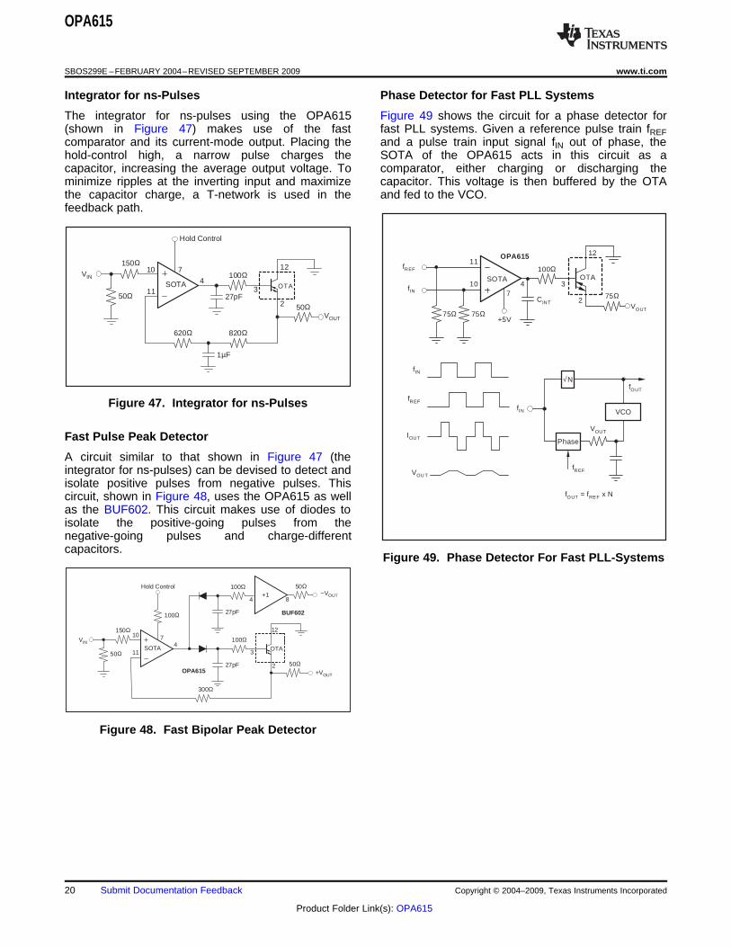
Integrator for ns-Pulses Phase Detector for Fast PLL Systems
The integrator for ns-pulses using the OPA615 Figure 49 shows the circuit for a phase detector for(shown in Figure 47) makes use of the fast fast PLL systems. Given a reference pulse train fREFcomparator and its current-mode output. Placing the and a pulse train input signal fIN out of phase, thehold-control high, a narrow pulse charges the SOTA of the OPA615 acts in this circuit as acapacitor, increasing the average output voltage. To comparator, either charging or discharging theminimize ripples at the inverting input and maximize capacitor. This voltage is then buffered by the OTAthe capacitor charge, a T-network is used in the and fed to the VCO.feedback path.
Figure 47. Integrator for ns-Pulses
Fast Pulse Peak Detector
A circuit similar to that shown in Figure 47 (theintegrator for ns-pulses) can be devised to detect andisolate positive pulses from negative pulses. Thiscircuit, shown in Figure 48, uses the OPA615 as wellas the BUF602. This circuit makes use of diodes toisolate the positive-going pulses from thenegative-going pulses and charge-differentcapacitors.
Figure 49. Phase Detector For Fast PLL-Systems
Figure 48. Fast Bipolar Peak Detector
20 Submit Documentation Feedback Copyright © 2004–2009, Texas Instruments Incorporated
Product Folder Link(s): OPA615

VOUT
VIN1
OPA694
SOTA
710
11 4
VHOLD1
27pF402Ω
50Ω
100Ω
100Ω
300Ω
300Ω
402Ω
402Ω
402Ω
OTA
12
2
3
VIN2
SOTA
710
11 4
VHOLD2
27pF50Ω
100Ω
100Ω
300Ω
300Ω
OTA
12
2
3
OPA615
www.ti.com...................................................................................................................................... SBOS299E –FEBRUARY 2004–REVISED SEPTEMBER 2009
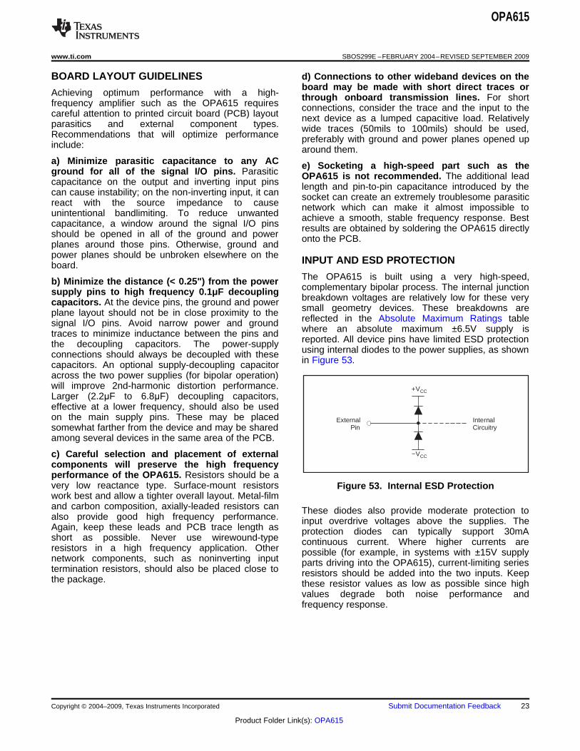
CORRELATED DOUBLE SAMPLER The signal coming from the CCD is applied to the twosample-and-hold amplifiers, with their outputs
Noise is the limiting factor for the resolution in a CCD connected to the difference amplifier. The timingsystem, where the kT/C noise is dominant (see diagram clarifies the operation (see Figure 52). AtFigure 51). To reduce this noise, imaging systems time t1, the sample and hold (S/H1) goes into the holduse a circuit called a Correlated Double Sampler mode, taking a sample of the reset level including the(CDS). The name comes from the double sampling noise. This voltage (VRESET) is applied to thetechnique of the CCD charge signal. A CDS using noninverting input of the difference amplifier. At timetwo OPA615s and one OPA694 is shown in t2, the sample-and-hold (S/H2) will take a sample ofFigure 50. The first sample (S1) is taken at the end of the video level, which is VRESET – VVIDEO. The outputthe reset period. When the reset switch opens again, voltage of the difference amplifier is defined by thethe effective noise bandwidth changes because of the equation VOUT = VIN+ – VIN–. The sample of the resetlarge difference in the switch RON and ROFF voltage contains the kT/C noise, which is eliminatedresistance. This difference causes the dominating by the subtraction of the difference amplifier.kT/C noise essentially to freeze in its last point.
The double sampling technique also reduces theThe other sample (S2) is taken during the video white noise. The white noise is part of the resetportion of the signal. Ideally, the two samples differ voltage (VRESET) as well as of the video amplitudeonly by a voltage corresponding to the transferred (VRESET – VVIDEO). With the assumption that the noisecharge signal. This is the video level minus the noise of the noise of the second sample was unchanged(ΔV). from the instant of the first sample, the noise
amplitudes are the same and are correlated in time.The CDS function will eliminate the kT/C noise asTherefore, the noise can be reduced by the CDSwell as much of the 1/f and white noise.function.
Figure 52 is a block diagram of a CDS circuit. Twosample-and-hold amplifiers and one differenceamplifier constitute the correlated double sampler.
Figure 50. Correlated Double Sampler
Copyright © 2004–2009, Texas Instruments Incorporated Submit Documentation Feedback 21
Product Folder Link(s): OPA615
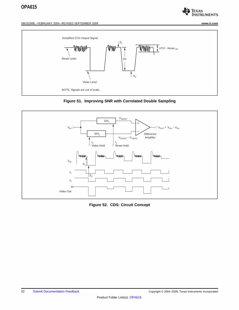
Reset Level
Simplified CCD Output Signal
NOTE: Signals are out of scale.
Video Level
S2
S1
∆V
kT/C −Noise PP
S/H1
VIN
t2Video Hold
S2
S1
VIN
t1
t2
Video Out
0V
S/H2
VRESET
VRESET − VVIDEO
DifferenceAmplifier
VOUT = VIN+ − VIN−
t1Reset Hold
OPA615
SBOS299E –FEBRUARY 2004–REVISED SEPTEMBER 2009...................................................................................................................................... www.ti.com
Figure 51. Improving SNR with Correlated Double Sampling
Figure 52. CDS: Circuit Concept
22 Submit Documentation Feedback Copyright © 2004–2009, Texas Instruments Incorporated
Product Folder Link(s): OPA615
ExternalPin
+VCC
−VCC
InternalCircuitry
OPA615
www.ti.com...................................................................................................................................... SBOS299E –FEBRUARY 2004–REVISED SEPTEMBER 2009
BOARD LAYOUT GUIDELINES d) Connections to other wideband devices on theboard may be made with short direct traces or
Achieving optimum performance with a high- through onboard transmission lines. For shortfrequency amplifier such as the OPA615 requires connections, consider the trace and the input to thecareful attention to printed circuit board (PCB) layout next device as a lumped capacitive load. Relativelyparasitics and external component types. wide traces (50mils to 100mils) should be used,Recommendations that will optimize performance preferably with ground and power planes opened upinclude: around them.a) Minimize parasitic capacitance to any AC e) Socketing a high-speed part such as theground for all of the signal I/O pins. Parasitic OPA615 is not recommended. The additional leadcapacitance on the output and inverting input pins length and pin-to-pin capacitance introduced by thecan cause instability; on the non-inverting input, it can socket can create an extremely troublesome parasiticreact with the source impedance to cause network which can make it almost impossible tounintentional bandlimiting. To reduce unwanted achieve a smooth, stable frequency response. Bestcapacitance, a window around the signal I/O pins results are obtained by soldering the OPA615 directlyshould be opened in all of the ground and power onto the PCB.planes around those pins. Otherwise, ground andpower planes should be unbroken elsewhere on the INPUT AND ESD PROTECTIONboard.
The OPA615 is built using a very high-speed,b) Minimize the distance (< 0.25") from the powercomplementary bipolar process. The internal junctionsupply pins to high frequency 0.1μF decouplingbreakdown voltages are relatively low for these verycapacitors. At the device pins, the ground and powersmall geometry devices. These breakdowns areplane layout should not be in close proximity to thereflected in the Absolute Maximum Ratings tablesignal I/O pins. Avoid narrow power and groundwhere an absolute maximum ±6.5V supply istraces to minimize inductance between the pins andreported. All device pins have limited ESD protectionthe decoupling capacitors. The power-supplyusing internal diodes to the power supplies, as shownconnections should always be decoupled with thesein Figure 53.capacitors. An optional supply-decoupling capacitor
across the two power supplies (for bipolar operation)will improve 2nd-harmonic distortion performance.Larger (2.2μF to 6.8μF) decoupling capacitors,effective at a lower frequency, should also be usedon the main supply pins. These may be placedsomewhat farther from the device and may be sharedamong several devices in the same area of the PCB.
c) Careful selection and placement of externalcomponents will preserve the high frequencyperformance of the OPA615. Resistors should be avery low reactance type. Surface-mount resistors Figure 53. Internal ESD Protectionwork best and allow a tighter overall layout. Metal-filmand carbon composition, axially-leaded resistors can These diodes also provide moderate protection toalso provide good high frequency performance. input overdrive voltages above the supplies. TheAgain, keep these leads and PCB trace length as protection diodes can typically support 30mAshort as possible. Never use wirewound-type continuous current. Where higher currents areresistors in a high frequency application. Other possible (for example, in systems with ±15V supplynetwork components, such as noninverting input parts driving into the OPA615), current-limiting seriestermination resistors, should also be placed close to resistors should be added into the two inputs. Keepthe package. these resistor values as low as possible since high
values degrade both noise performance andfrequency response.
Copyright © 2004–2009, Texas Instruments Incorporated Submit Documentation Feedback 23
Product Folder Link(s): OPA615
OPA615
SBOS299E –FEBRUARY 2004–REVISED SEPTEMBER 2009...................................................................................................................................... www.ti.com
REVISION HISTORY
NOTE: Page numbers for previous revisions may differ from page numbers in the current version.
Changes from Revision D (August 2008) to Revision E ................................................................................................ Page
• Corrected y-axis title of Figure 25 ....................................................................................................................................... 10
Changes from Revision C (October 2006) to Revision D ............................................................................................... Page
• Changed rating for storage temperature range in Absolute Maximum Ratings table from –40°C to +125°C to –65°Cto +125°C .............................................................................................................................................................................. 2
• Clarified hold control pin voltage rating in Absolute Maximum Ratings table ....................................................................... 2
24 Submit Documentation Feedback Copyright © 2004–2009, Texas Instruments Incorporated
Product Folder Link(s): OPA615
PACKAGE OPTION ADDENDUM
www.ti.com 7-Apr-2016
Addendum-Page 1
PACKAGING INFORMATION
Orderable Device Status(1)
Package Type PackageDrawing
Pins PackageQty
Eco Plan(2)
Lead/Ball Finish(6)
MSL Peak Temp(3)
Op Temp (°C) Device Marking(4/5)
Samples
OPA615ID ACTIVE SOIC D 14 50 Green (RoHS& no Sb/Br)
CU NIPDAU Level-2-260C-1 YEAR -40 to 85 OPA615ID
OPA615IDGSR ACTIVE VSSOP DGS 10 2500 Green (RoHS& no Sb/Br)
CU NIPDAUAG Level-2-260C-1 YEAR -40 to 85 BJT
OPA615IDGST ACTIVE VSSOP DGS 10 250 Green (RoHS& no Sb/Br)
CU NIPDAUAG Level-2-260C-1 YEAR -40 to 85 BJT
OPA615IDR ACTIVE SOIC D 14 2500 Green (RoHS& no Sb/Br)
CU NIPDAU Level-2-260C-1 YEAR -40 to 85 OPA615ID
OPA615IDRG4 ACTIVE SOIC D 14 2500 Green (RoHS& no Sb/Br)
CU NIPDAU Level-2-260C-1 YEAR -40 to 85 OPA615ID
(1) The marketing status values are defined as follows:ACTIVE: Product device recommended for new designs.LIFEBUY: TI has announced that the device will be discontinued, and a lifetime-buy period is in effect.NRND: Not recommended for new designs. Device is in production to support existing customers, but TI does not recommend using this part in a new design.PREVIEW: Device has been announced but is not in production. Samples may or may not be available.OBSOLETE: TI has discontinued the production of the device.
(2) Eco Plan - The planned eco-friendly classification: Pb-Free (RoHS), Pb-Free (RoHS Exempt), or Green (RoHS & no Sb/Br) - please check http://www.ti.com/productcontent for the latest availabilityinformation and additional product content details.TBD: The Pb-Free/Green conversion plan has not been defined.Pb-Free (RoHS): TI's terms "Lead-Free" or "Pb-Free" mean semiconductor products that are compatible with the current RoHS requirements for all 6 substances, including the requirement thatlead not exceed 0.1% by weight in homogeneous materials. Where designed to be soldered at high temperatures, TI Pb-Free products are suitable for use in specified lead-free processes.Pb-Free (RoHS Exempt): This component has a RoHS exemption for either 1) lead-based flip-chip solder bumps used between the die and package, or 2) lead-based die adhesive used betweenthe die and leadframe. The component is otherwise considered Pb-Free (RoHS compatible) as defined above.Green (RoHS & no Sb/Br): TI defines "Green" to mean Pb-Free (RoHS compatible), and free of Bromine (Br) and Antimony (Sb) based flame retardants (Br or Sb do not exceed 0.1% by weightin homogeneous material)
(3) MSL, Peak Temp. - The Moisture Sensitivity Level rating according to the JEDEC industry standard classifications, and peak solder temperature.
(4) There may be additional marking, which relates to the logo, the lot trace code information, or the environmental category on the device.
(5) Multiple Device Markings will be inside parentheses. Only one Device Marking contained in parentheses and separated by a "~" will appear on a device. If a line is indented then it is a continuationof the previous line and the two combined represent the entire Device Marking for that device.
PACKAGE OPTION ADDENDUM
www.ti.com 7-Apr-2016
Addendum-Page 2
(6) Lead/Ball Finish - Orderable Devices may have multiple material finish options. Finish options are separated by a vertical ruled line. Lead/Ball Finish values may wrap to two lines if the finishvalue exceeds the maximum column width.
Important Information and Disclaimer:The information provided on this page represents TI's knowledge and belief as of the date that it is provided. TI bases its knowledge and belief on informationprovided by third parties, and makes no representation or warranty as to the accuracy of such information. Efforts are underway to better integrate information from third parties. TI has taken andcontinues to take reasonable steps to provide representative and accurate information but may not have conducted destructive testing or chemical analysis on incoming materials and chemicals.TI and TI suppliers consider certain information to be proprietary, and thus CAS numbers and other limited information may not be available for release.
In no event shall TI's liability arising out of such information exceed the total purchase price of the TI part(s) at issue in this document sold by TI to Customer on an annual basis.
TAPE AND REEL INFORMATION
*All dimensions are nominal
Device PackageType
PackageDrawing
Pins SPQ ReelDiameter
(mm)
ReelWidth
W1 (mm)
A0(mm)
B0(mm)
K0(mm)
P1(mm)
W(mm)
Pin1Quadrant
OPA615IDGSR VSSOP DGS 10 2500 330.0 12.4 5.3 3.4 1.4 8.0 12.0 Q1
OPA615IDGST VSSOP DGS 10 250 180.0 12.4 5.3 3.4 1.4 8.0 12.0 Q1
OPA615IDR SOIC D 14 2500 330.0 16.4 6.5 9.0 2.1 8.0 16.0 Q1
PACKAGE MATERIALS INFORMATION
www.ti.com 2-Sep-2013
Pack Materials-Page 1
*All dimensions are nominal
Device Package Type Package Drawing Pins SPQ Length (mm) Width (mm) Height (mm)
OPA615IDGSR VSSOP DGS 10 2500 367.0 367.0 35.0
OPA615IDGST VSSOP DGS 10 250 210.0 185.0 35.0
OPA615IDR SOIC D 14 2500 367.0 367.0 38.0
PACKAGE MATERIALS INFORMATION
www.ti.com 2-Sep-2013
Pack Materials-Page 2


IMPORTANT NOTICE
Texas Instruments Incorporated and its subsidiaries (TI) reserve the right to make corrections, enhancements, improvements and otherchanges to its semiconductor products and services per JESD46, latest issue, and to discontinue any product or service per JESD48, latestissue. Buyers should obtain the latest relevant information before placing orders and should verify that such information is current andcomplete. All semiconductor products (also referred to herein as “components”) are sold subject to TI’s terms and conditions of salesupplied at the time of order acknowledgment.TI warrants performance of its components to the specifications applicable at the time of sale, in accordance with the warranty in TI’s termsand conditions of sale of semiconductor products. Testing and other quality control techniques are used to the extent TI deems necessaryto support this warranty. Except where mandated by applicable law, testing of all parameters of each component is not necessarilyperformed.TI assumes no liability for applications assistance or the design of Buyers’ products. Buyers are responsible for their products andapplications using TI components. To minimize the risks associated with Buyers’ products and applications, Buyers should provideadequate design and operating safeguards.TI does not warrant or represent that any license, either express or implied, is granted under any patent right, copyright, mask work right, orother intellectual property right relating to any combination, machine, or process in which TI components or services are used. Informationpublished by TI regarding third-party products or services does not constitute a license to use such products or services or a warranty orendorsement thereof. Use of such information may require a license from a third party under the patents or other intellectual property of thethird party, or a license from TI under the patents or other intellectual property of TI.Reproduction of significant portions of TI information in TI data books or data sheets is permissible only if reproduction is without alterationand is accompanied by all associated warranties, conditions, limitations, and notices. TI is not responsible or liable for such altereddocumentation. Information of third parties may be subject to additional restrictions.Resale of TI components or services with statements different from or beyond the parameters stated by TI for that component or servicevoids all express and any implied warranties for the associated TI component or service and is an unfair and deceptive business practice.TI is not responsible or liable for any such statements.Buyer acknowledges and agrees that it is solely responsible for compliance with all legal, regulatory and safety-related requirementsconcerning its products, and any use of TI components in its applications, notwithstanding any applications-related information or supportthat may be provided by TI. Buyer represents and agrees that it has all the necessary expertise to create and implement safeguards whichanticipate dangerous consequences of failures, monitor failures and their consequences, lessen the likelihood of failures that might causeharm and take appropriate remedial actions. Buyer will fully indemnify TI and its representatives against any damages arising out of the useof any TI components in safety-critical applications.In some cases, TI components may be promoted specifically to facilitate safety-related applications. With such components, TI’s goal is tohelp enable customers to design and create their own end-product solutions that meet applicable functional safety standards andrequirements. Nonetheless, such components are subject to these terms.No TI components are authorized for use in FDA Class III (or similar life-critical medical equipment) unless authorized officers of the partieshave executed a special agreement specifically governing such use.Only those TI components which TI has specifically designated as military grade or “enhanced plastic” are designed and intended for use inmilitary/aerospace applications or environments. Buyer acknowledges and agrees that any military or aerospace use of TI componentswhich have not been so designated is solely at the Buyer's risk, and that Buyer is solely responsible for compliance with all legal andregulatory requirements in connection with such use.TI has specifically designated certain components as meeting ISO/TS16949 requirements, mainly for automotive use. In any case of use ofnon-designated products, TI will not be responsible for any failure to meet ISO/TS16949.
Products ApplicationsAudio www.ti.com/audio Automotive and Transportation www.ti.com/automotiveAmplifiers amplifier.ti.com Communications and Telecom www.ti.com/communicationsData Converters dataconverter.ti.com Computers and Peripherals www.ti.com/computersDLP® Products www.dlp.com Consumer Electronics www.ti.com/consumer-appsDSP dsp.ti.com Energy and Lighting www.ti.com/energyClocks and Timers www.ti.com/clocks Industrial www.ti.com/industrialInterface interface.ti.com Medical www.ti.com/medicalLogic logic.ti.com Security www.ti.com/securityPower Mgmt power.ti.com Space, Avionics and Defense www.ti.com/space-avionics-defenseMicrocontrollers microcontroller.ti.com Video and Imaging www.ti.com/videoRFID www.ti-rfid.comOMAP Applications Processors www.ti.com/omap TI E2E Community e2e.ti.comWireless Connectivity www.ti.com/wirelessconnectivity
Mailing Address: Texas Instruments, Post Office Box 655303, Dallas, Texas 75265Copyright © 2016, Texas Instruments Incorporated