Embed Size (px)
Citation preview
+
William Stallings
Computer Organization
and Architecture
10th Edition
© 2016 Pearson Education, Inc., Hoboken,
NJ. All rights reserved.
+ Chapter 5Internal Memory
© 2016 Pearson Education, Inc., Hoboken, NJ. All rights reserved.
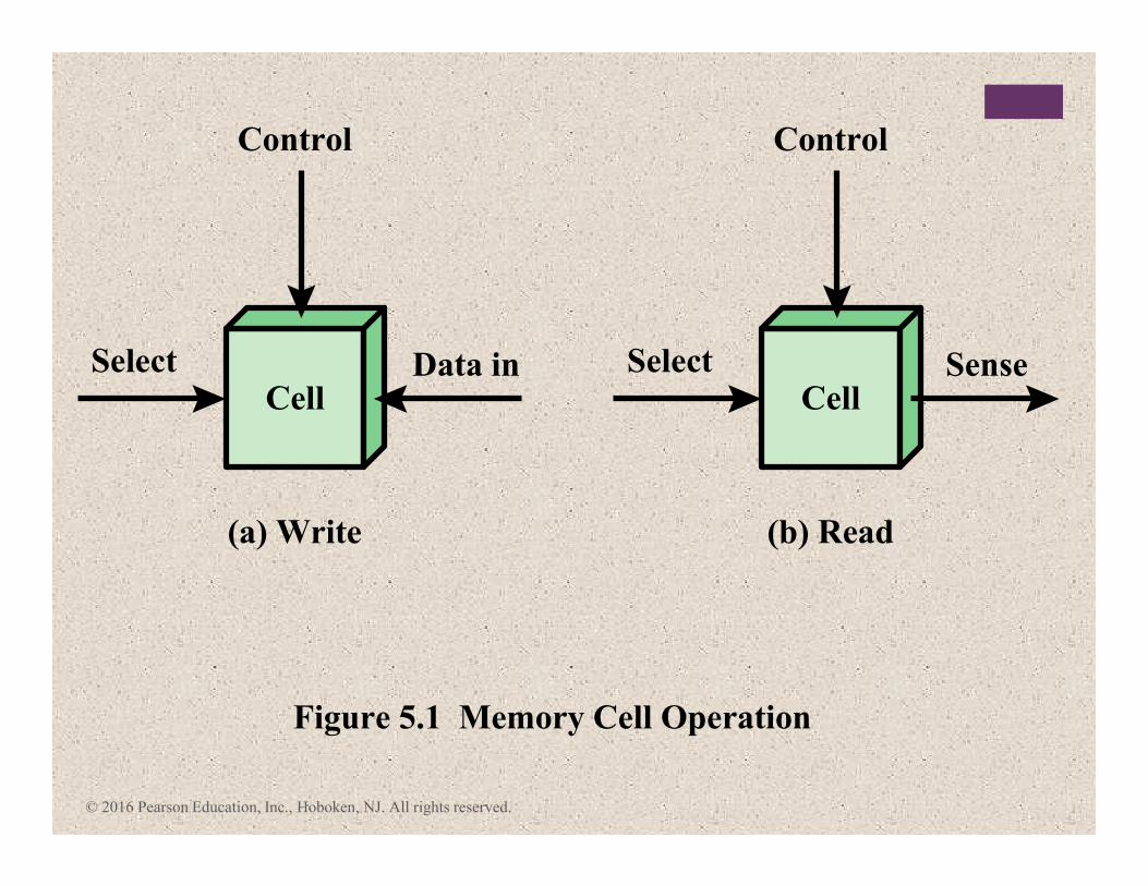
CellSelect Data in
Control
(a) Write
CellSelect Sense
Figure 5.1 Memory Cell Operation
Control
(b) Read
© 2016 Pearson Education, Inc., Hoboken, NJ. All rights reserved.
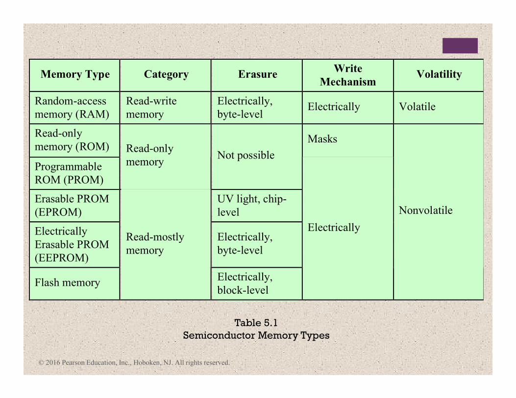
Table 5.1
Semiconductor Memory Types
Memory Type Category Erasure Write
Mechanism Volatility
Random-access
memory (RAM)
Read-write
memory
Electrically,
byte-level Electrically Volatile
Read-only
memory (ROM) Masks
Programmable
ROM (PROM)
Read-only
memory Not possible
Erasable PROM
(EPROM)
UV light, chip-
level
Electrically
Erasable PROM
(EEPROM)
Electrically,
byte-level
Flash memory
Read-mostly
memory
Electrically,
block-level
Electrically
Nonvolatile
© 2016 Pearson Education, Inc., Hoboken, NJ. All rights reserved.
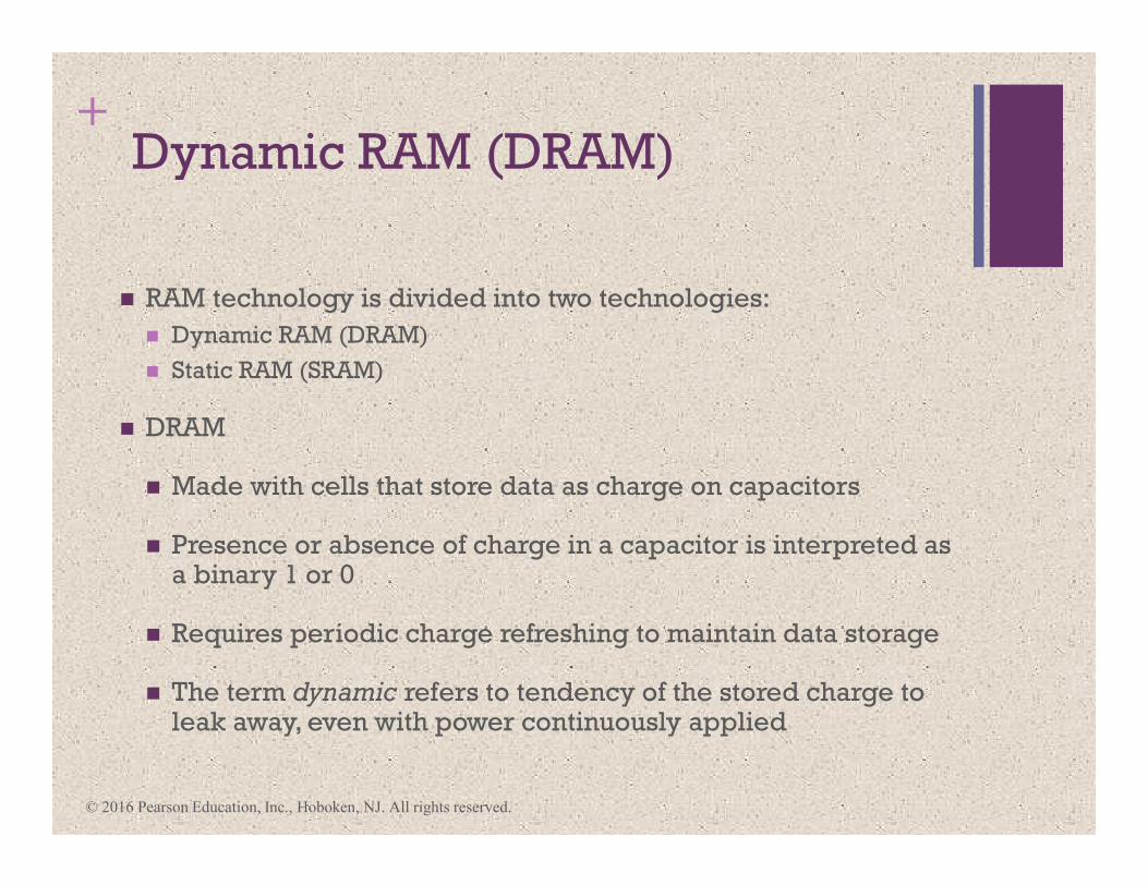
+Dynamic RAM (DRAM)
� RAM technology is divided into two technologies:
� Dynamic RAM (DRAM)
� Static RAM (SRAM)
� DRAM
� Made with cells that store data as charge on capacitors
� Presence or absence of charge in a capacitor is interpreted as a binary 1 or 0
� Requires periodic charge refreshing to maintain data storage
� The term dynamic refers to tendency of the stored charge to leak away, even with power continuously applied
© 2016 Pearson Education, Inc., Hoboken, NJ. All rights reserved.
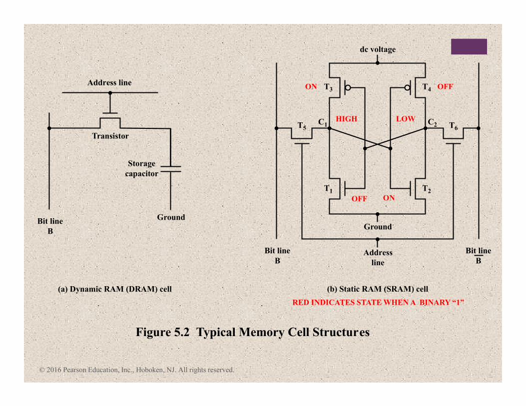
Address line
Ground
dc voltage
Address
line
(b) Static RAM (SRAM) cell
Figure 5.2 Typical Memory Cell Structures
(a) Dynamic RAM (DRAM) cell
Bit line
B
C1
T1 T2
T3
T5 T6
T4
C2
Bit line
B
Bit line
B
Transistor
Ground
Storage
capacitor
© 2016 Pearson Education, Inc., Hoboken, NJ. All rights reserved.
HIGH LOW
OFF
OFFON
ON
RED INDICATES STATE WHEN A BINARY “1”
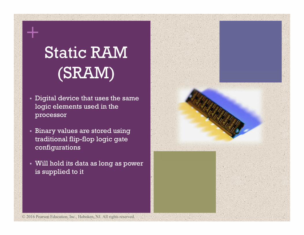
+Static RAM
(SRAM)
� Digital device that uses the same
logic elements used in the
processor
� Binary values are stored using
traditional flip-flop logic gate
configurations
� Will hold its data as long as power
is supplied to it
© 2016 Pearson Education, Inc., Hoboken, NJ. All rights reserved.
+
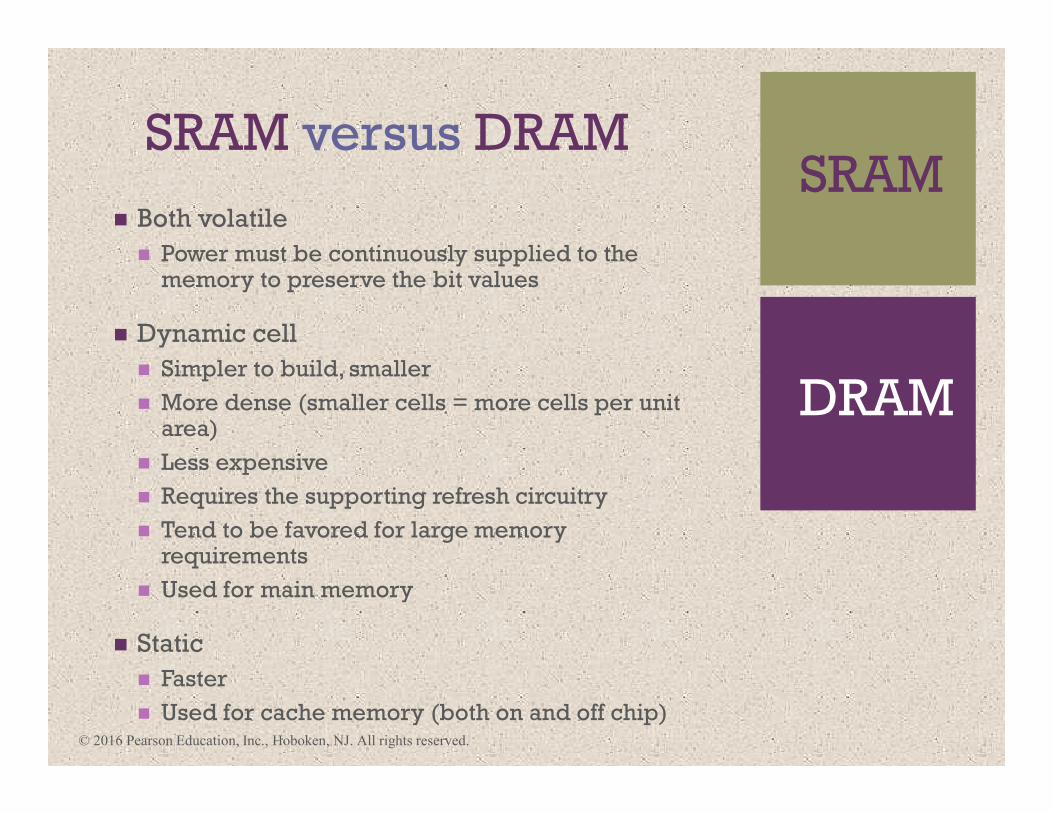
SRAM versus DRAM
� Both volatile
� Power must be continuously supplied to the memory to preserve the bit values
� Dynamic cell
� Simpler to build, smaller
� More dense (smaller cells = more cells per unit area)
� Less expensive
� Requires the supporting refresh circuitry
� Tend to be favored for large memory requirements
� Used for main memory
� Static
� Faster
� Used for cache memory (both on and off chip)
SRAM
DRAM
© 2016 Pearson Education, Inc., Hoboken, NJ. All rights reserved.
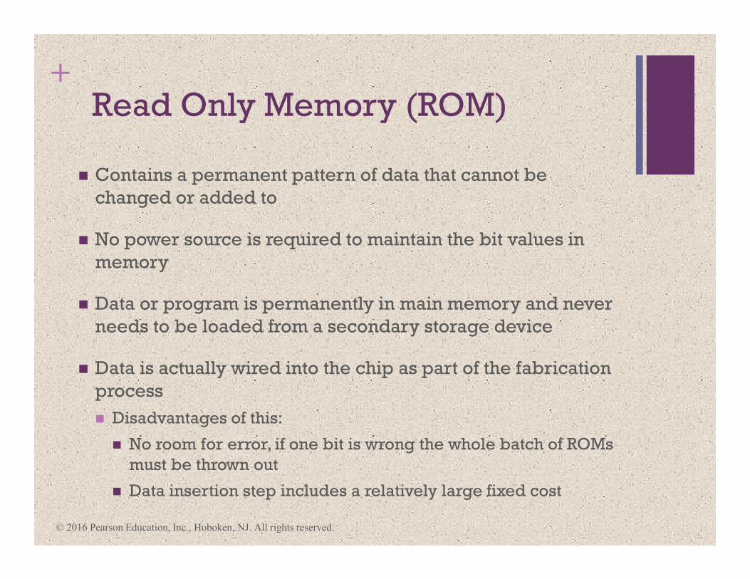
+Read Only Memory (ROM)
� Contains a permanent pattern of data that cannot be
changed or added to
� No power source is required to maintain the bit values in
memory
� Data or program is permanently in main memory and never
needs to be loaded from a secondary storage device
� Data is actually wired into the chip as part of the fabrication
process
� Disadvantages of this:
� No room for error, if one bit is wrong the whole batch of ROMs
must be thrown out
� Data insertion step includes a relatively large fixed cost
© 2016 Pearson Education, Inc., Hoboken, NJ. All rights reserved.
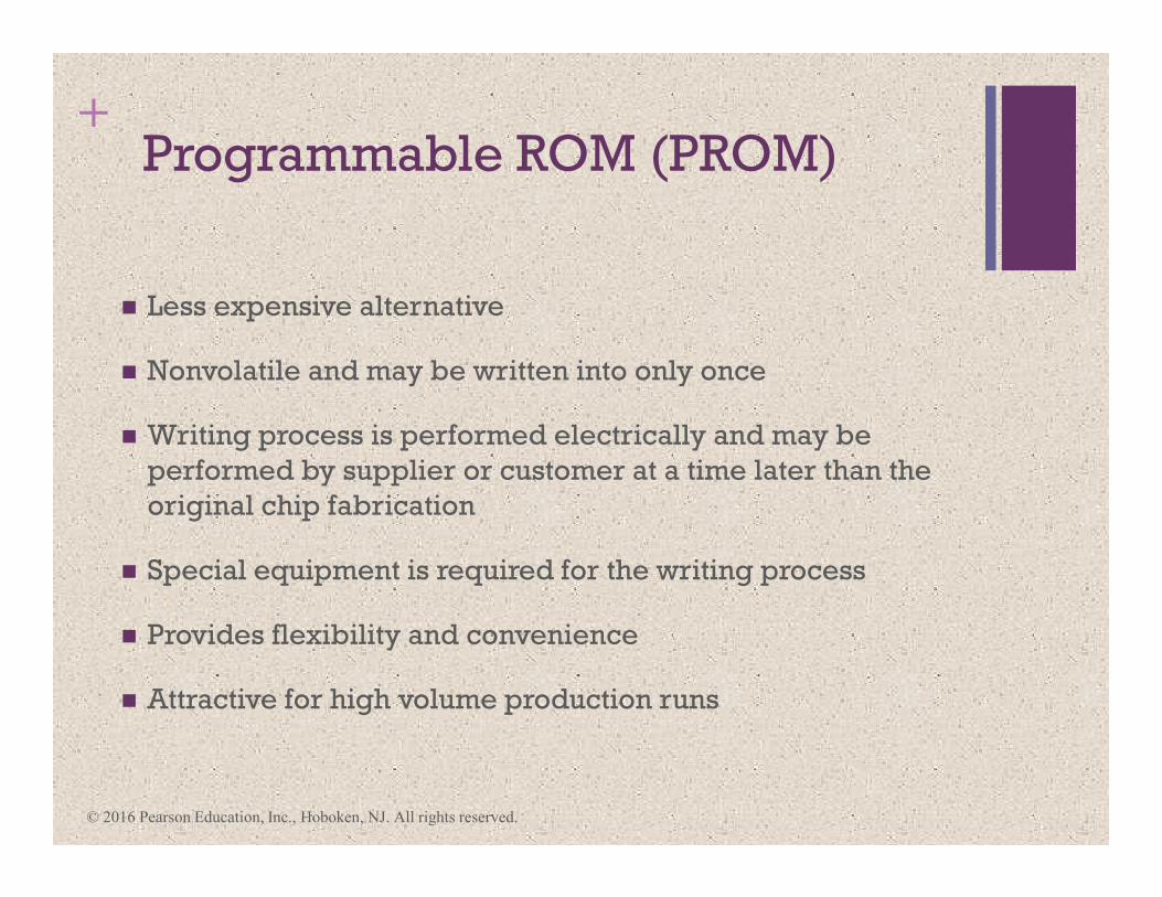
+Programmable ROM (PROM)
� Less expensive alternative
� Nonvolatile and may be written into only once
� Writing process is performed electrically and may be
performed by supplier or customer at a time later than the
original chip fabrication
� Special equipment is required for the writing process
� Provides flexibility and convenience
� Attractive for high volume production runs
© 2016 Pearson Education, Inc., Hoboken, NJ. All rights reserved.
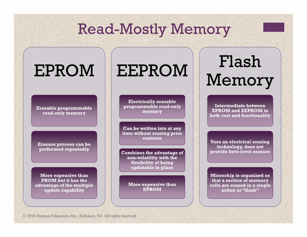
Read-Mostly Memory
EPROM
Erasable programmable read-only memory
Erasure process can be performed repeatedly
More expensive than PROM but it has the
advantage of the multiple update capability
EEPROM
Electrically erasable programmable read-only
memory
Can be written into at any time without erasing prior
contents
Combines the advantage of non-volatility with the
flexibility of being updatable in place
More expensive than EPROM
Flash Memory
Intermediate between EPROM and EEPROM in
both cost and functionality
Uses an electrical erasing technology, does not
provide byte-level erasure
Microchip is organized so that a section of memory
cells are erased in a single action or “flash”
© 2016 Pearson Education, Inc., Hoboken, NJ. All rights reserved.
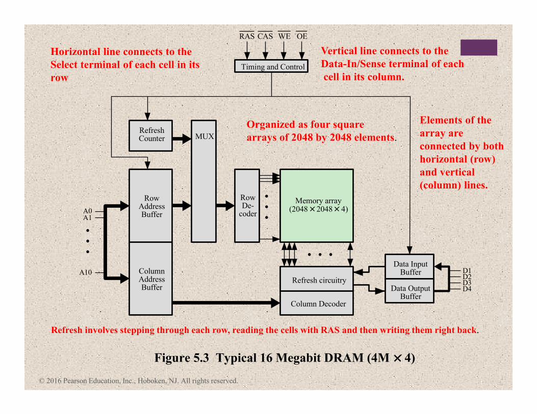
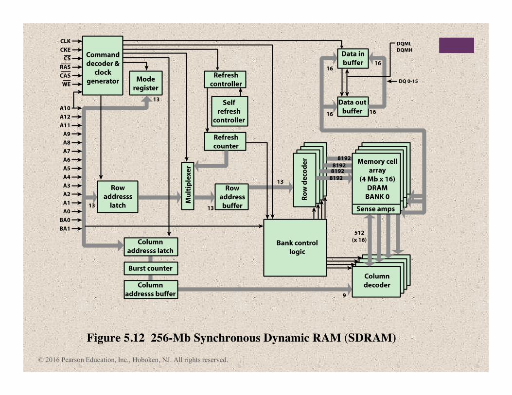
Column Decoder
Refresh circuitry
Memory array(2048 2048 4)
RowDe-
coderA0A1
A10
RowAddressBuffer
ColumnAddressBuffer
Timing and Control
RAS CAS WE OE
MUXRefreshCounter
Data InputBuffer
Data OutputBuffer
D1D2D3D4
Figure 5.3 Typical 16 Megabit DRAM (4M 4)
© 2016 Pearson Education, Inc., Hoboken, NJ. All rights reserved.
Organized as four square
arrays of 2048 by 2048 elements.
Elements of the
array are
connected by both
horizontal (row)
and vertical
(column) lines.
Horizontal line connects to the
Select terminal of each cell in its
row
Vertical line connects to the
Data-In/Sense terminal of each
cell in its column.
Refresh involves stepping through each row, reading the cells with RAS and then writing them right back.
© 2016 Pearson Education, Inc., Hoboken, NJ. All rights reserved.
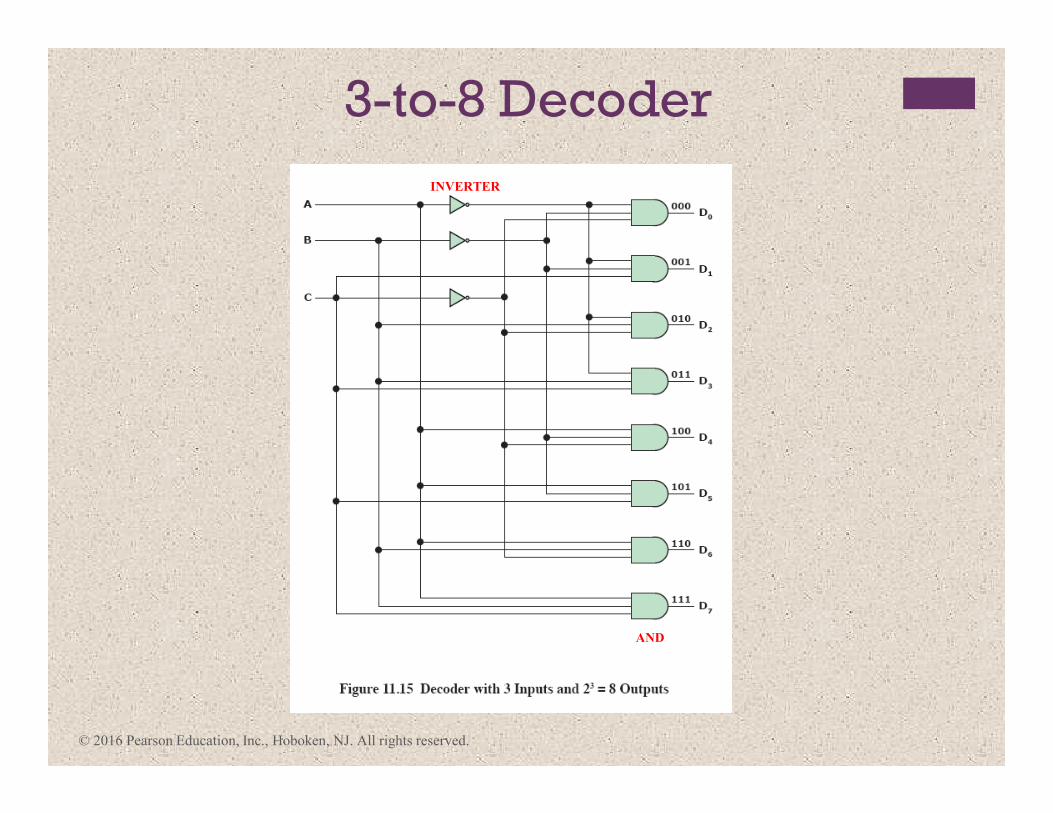
3-to-8 Decoder
INVERTER
AND
© 2016 Pearson Education, Inc., Hoboken, NJ. All rights reserved.
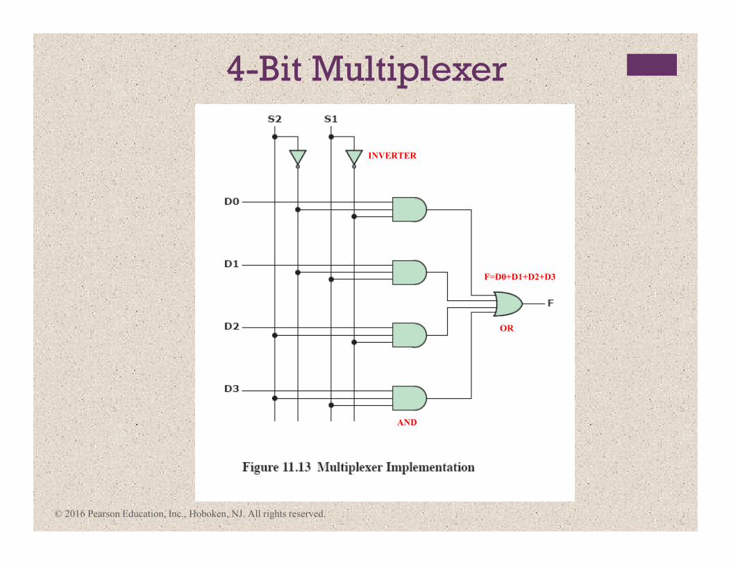
4-Bit Multiplexer
INVERTER
AND
OR
F=D0+D1+D2+D3
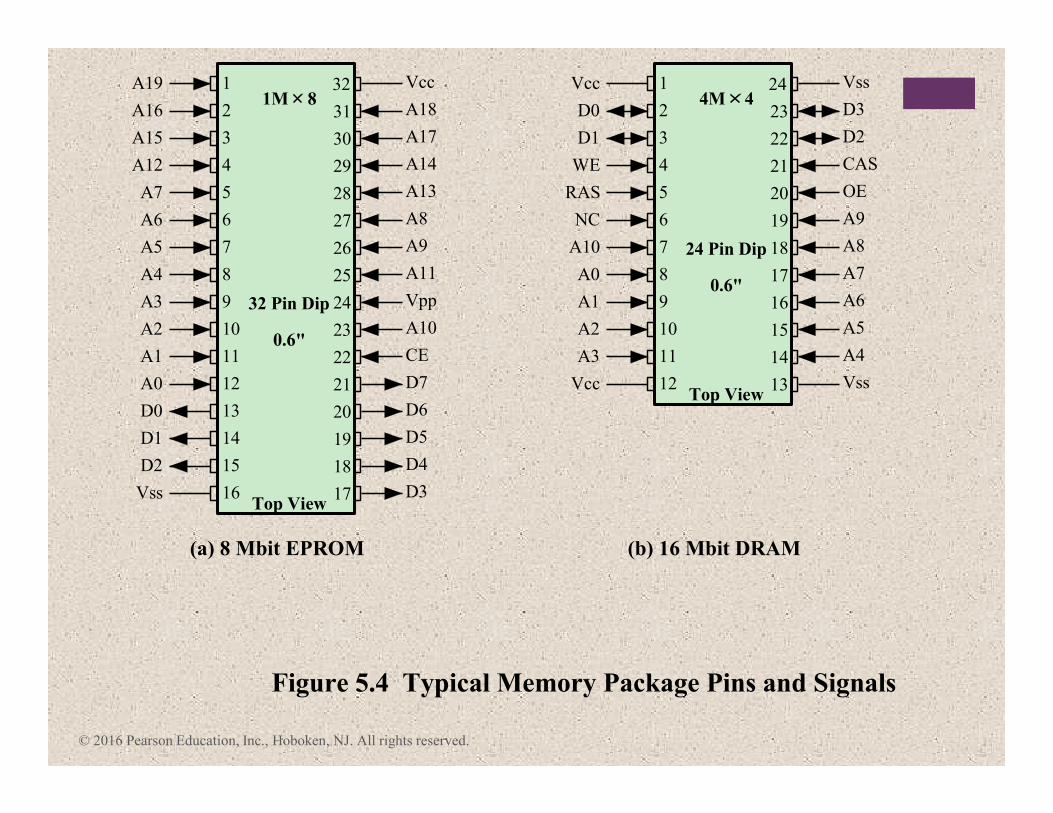
4M 4
24 Pin Dip
0.6"
Top View
Figure 5.4 Typical Memory Package Pins and Signals
32
31
30
29
28
27
26
25
24
23
22
21
20
19
18
17
1
2
3
4
5
6
7
8
9
10
11
12
13
14
15
16
A19
A16
A15
A12
A7
A6
A5
A4
A3
A2
A1
A0
D0
D1
D2
Vss
Vcc
A18
A17
A14
A13
A8
A9
A11
Vpp
A10
CE
D7
D6
D5
D4
D3
32 Pin Dip
0.6"
Top View
1M 824
23
22
21
20
19
18
17
16
15
14
13
1
2
3
4
5
6
7
8
9
10
11
12
Vcc
D0
D1
WE
RAS
NC
A10
A0
A1
A2
A3
Vcc
Vss
D3
D2
CAS
OE
A9
A8
A7
A6
A5
A4
Vss
(a) 8 Mbit EPROM (b) 16 Mbit DRAM
© 2016 Pearson Education, Inc., Hoboken, NJ. All rights reserved.
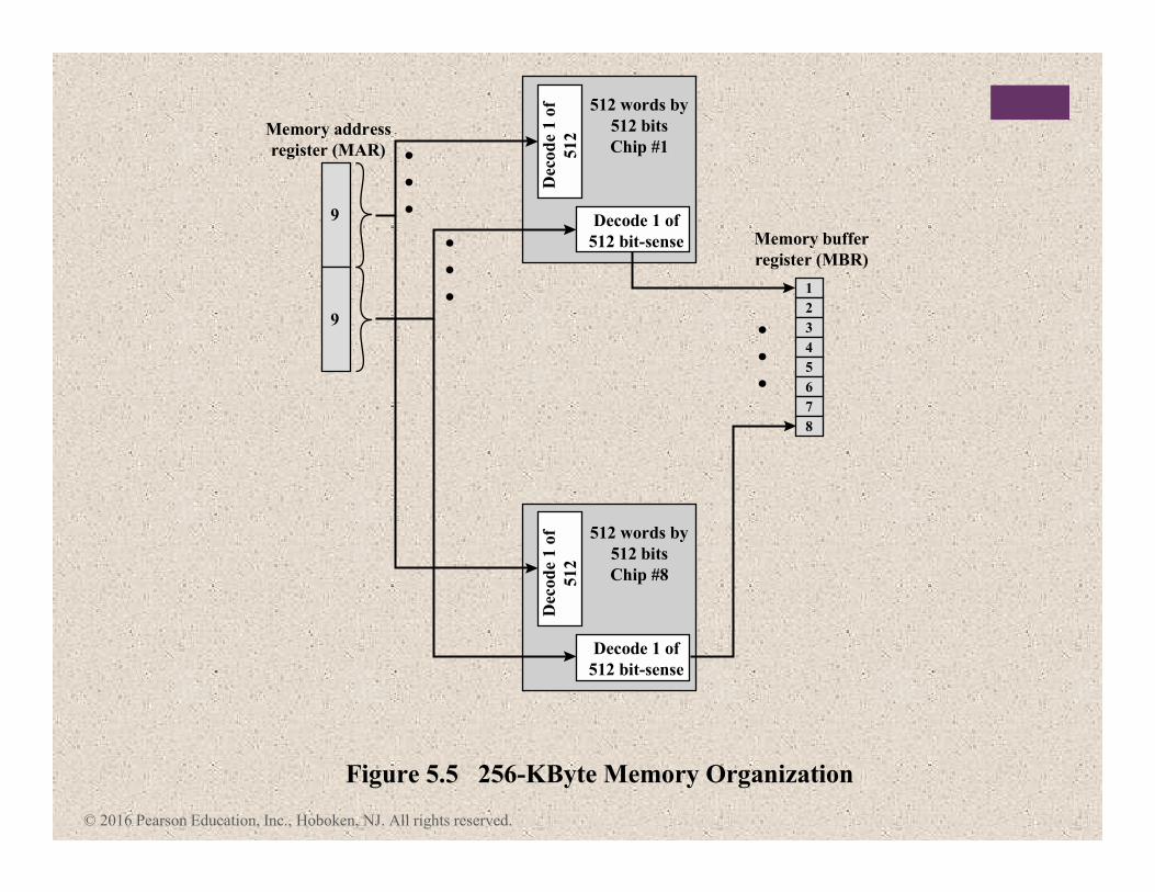
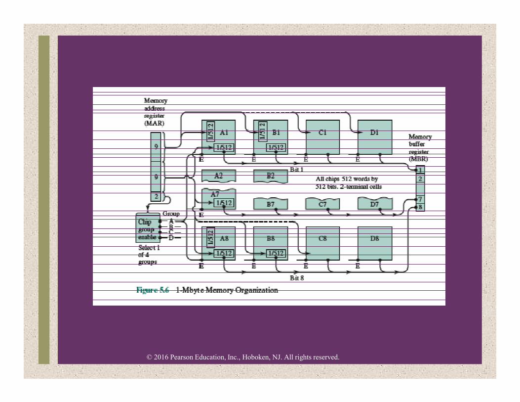
512 words by
512 bits
Chip #1
Memory buffer
register (MBR)
Figure 5.5 256-KByte Memory Organization
Memory address
register (MAR)
Decode 1 of
512 bit-sense
Dec
od
e 1 o
f
512
512 words by
512 bits
Chip #8
Decode 1 of
512 bit-sense
Dec
od
e 1 o
f
51
2
1
9
92
3
4
5
6
7
8
© 2016 Pearson Education, Inc., Hoboken, NJ. All rights reserved.
+
© 2016 Pearson Education, Inc., Hoboken, NJ. All rights reserved.
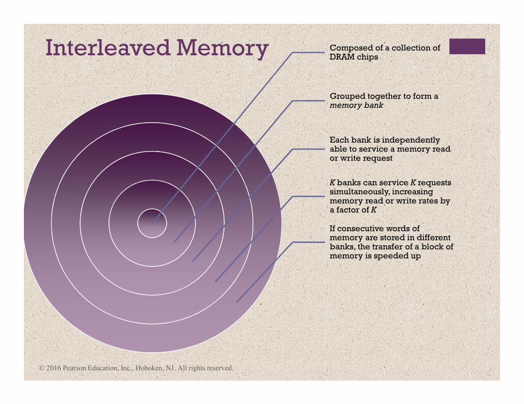
Interleaved Memory Composed of a collection of DRAM chips
Grouped together to form a memory bank
Each bank is independently able to service a memory read or write request
K banks can service K requests simultaneously, increasing memory read or write rates by a factor of K
If consecutive words of memory are stored in different banks, the transfer of a block of memory is speeded up
© 2016 Pearson Education, Inc., Hoboken, NJ. All rights reserved.
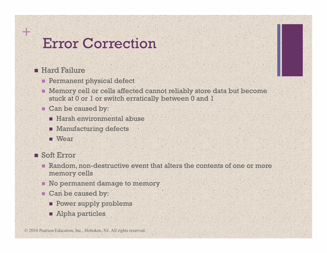
+Error Correction
� Hard Failure
� Permanent physical defect
� Memory cell or cells affected cannot reliably store data but become stuck at 0 or 1 or switch erratically between 0 and 1
� Can be caused by:
� Harsh environmental abuse
� Manufacturing defects
� Wear
� Soft Error
� Random, non-destructive event that alters the contents of one or more memory cells
� No permanent damage to memory
� Can be caused by:
� Power supply problems
� Alpha particles
© 2016 Pearson Education, Inc., Hoboken, NJ. All rights reserved.
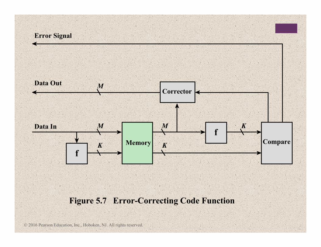
f
fCompare
Corrector
Memory
Figure 5.7 Error-Correcting Code Function
Data In
Data Out
Error Signal
M
K
M
M
K
K
© 2016 Pearson Education, Inc., Hoboken, NJ. All rights reserved.
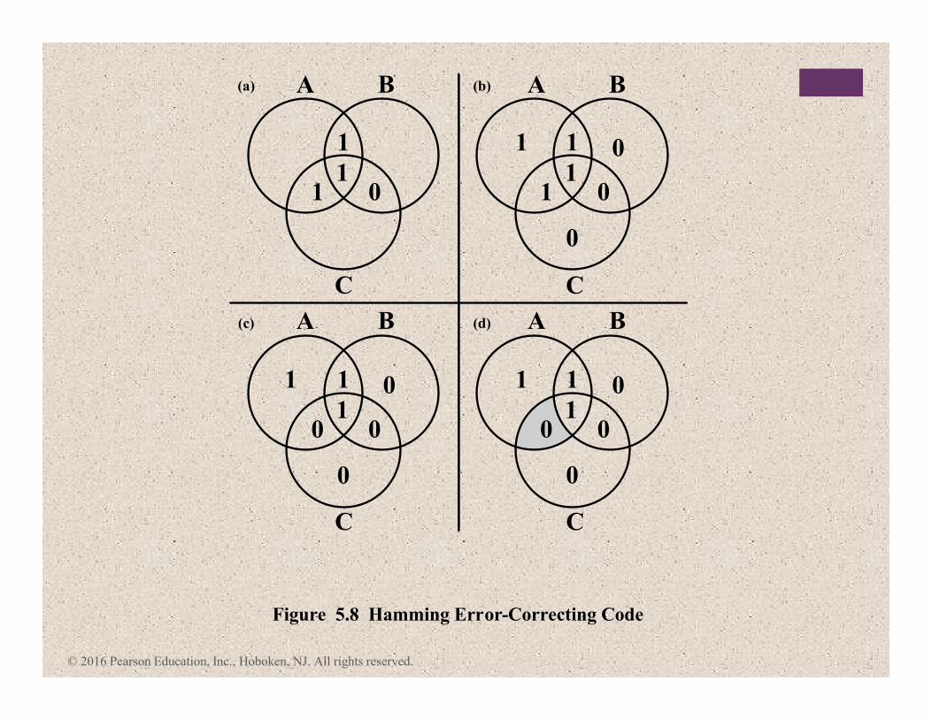
1 1
10
00
(d)(c)
0
1 1
10
00
0
Figure 5.8 Hamming Error-Correcting Code
1 1
10
01
(b)(a)
0
1
A B
C
A B
C
A B
C
A B
C
101
© 2016 Pearson Education, Inc., Hoboken, NJ. All rights reserved.
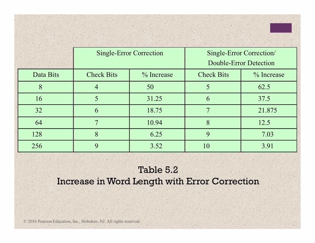
Single-Error Correction Single-Error Correction/
Double-Error Detection
Data Bits Check Bits % Increase Check Bits % Increase
8 4 50 5 62.5
16 5 31.25 6 37.5
32 6 18.75 7 21.875
64 7 10.94 8 12.5
128 8 6.25 9 7.03
256 9 3.52 10 3.91
Table 5.2
Increase in Word Length with Error Correction
© 2016 Pearson Education, Inc., Hoboken, NJ. All rights reserved.
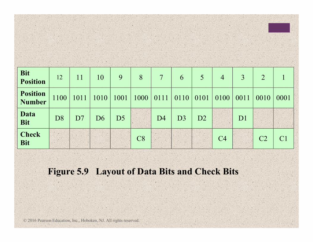
Bit
Position 12 11 10 9 8 7 6 5 4 3 2 1
Position
Number 1100 1011 1010 1001 1000 0111 0110 0101 0100 0011 0010 0001
Data
Bit D8 D7 D6 D5 D4 D3 D2 D1
Check
Bit C8 C4 C2 C1
Figure 5.9 Layout of Data Bits and Check Bits
© 2016 Pearson Education, Inc., Hoboken, NJ. All rights reserved.
© 2016 Pearson Education, Inc., Hoboken, NJ. All rights reserved.
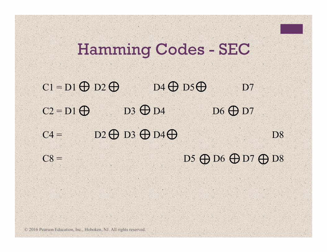
C1 = D1 D2 D4 D5 D7
C2 = D1 D3 D4 D6 D7
C4 = D2 D3 D4 D8
C8 = D5 D6 D7 D8
Hamming Codes - SEC
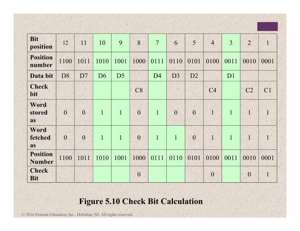
Bit
position 12 11 10 9 8 7 6 5 4 3 2 1
Position
number 1100 1011 1010 1001 1000 0111 0110 0101 0100 0011 0010 0001
Data bit D8 D7 D6 D5 D4 D3 D2 D1
Check
bit C8 C4 C2 C1
Word
stored
as
0 0 1 1 0 1 0 0 1 1 1 1
Word
fetched
as
0 0 1 1 0 1 1 0 1 1 1 1
Position
Number 1100 1011 1010 1001 1000 0111 0110 0101 0100 0011 0010 0001
Check
Bit 0 0 0 1
Figure 5.10 Check Bit Calculation
© 2016 Pearson Education, Inc., Hoboken, NJ. All rights reserved.
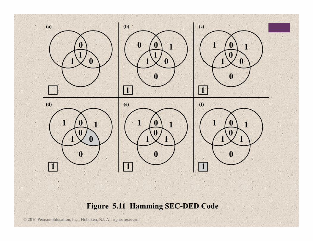
1 0
01
11
(e)(d)
0
Figure 5.11 Hamming SEC-DED Code
0 0
11
01
(b)(a)
0
0
101
1 1
1 1 1
1 0
01
11
(f)
0
1 0
01
01
(c)
0
1 0
01
01
0
© 2016 Pearson Education, Inc., Hoboken, NJ. All rights reserved.
+
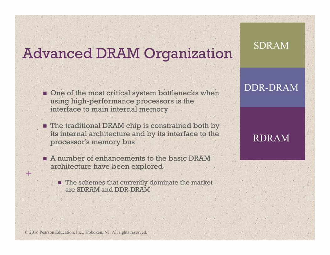
Advanced DRAM Organization
� One of the most critical system bottlenecks when using high-performance processors is the interface to main internal memory
� The traditional DRAM chip is constrained both by its internal architecture and by its interface to the processor’s memory bus
� A number of enhancements to the basic DRAM architecture have been explored
� The schemes that currently dominate the market are SDRAM and DDR-DRAM
SDRAM
RDRAM
DDR-DRAM
© 2016 Pearson Education, Inc., Hoboken, NJ. All rights reserved.
Synchronous DRAM (SDRAM)
One of the most widely used forms of DRAM
Exchanges data with the processor synchronized to an external clock signal and running at the full
speed of the processor/memory bus without imposing wait states
Exchanges data with the processor synchronized to an external clock signal and running at the full
speed of the processor/memory bus without imposing wait states
With synchronous access the DRAM moves data in and out under control of the system clock
• The processor or other master issues the instruction and address information which is latched by the DRAM
• The DRAM then responds after a set number of clock cycles
• Meanwhile the master can safely do other tasks while the SDRAM is processing
© 2016 Pearson Education, Inc., Hoboken, NJ. All rights reserved.
© 2016 Pearson Education, Inc., Hoboken, NJ. All rights reserved.
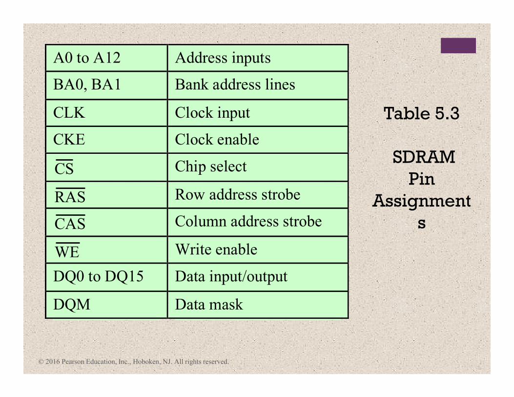
Table 5.3
SDRAM
Pin
Assignment
s
A0 to A12 Address inputs
BA0, BA1 Bank address lines
CLK Clock input
CKE Clock enable
CS Chip select
RAS Row address strobe
CAS Column address strobe
WE Write enable
DQ0 to DQ15 Data input/output
DQM Data mask
© 2016 Pearson Education, Inc., Hoboken, NJ. All rights reserved.
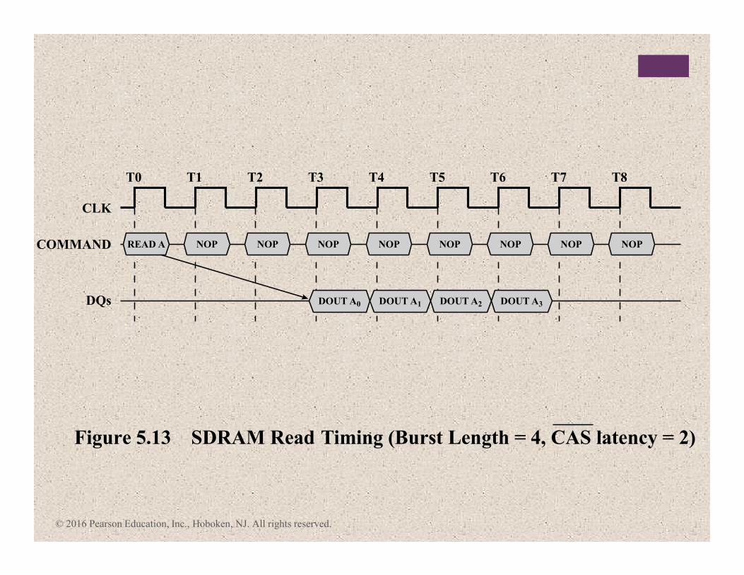
T0
CLK
COMMAND
Figure 5.13 SDRAM Read Timing (Burst Length = 4, CAS latency = 2)
DQs
T1 T2 T3 T4 T5 T6 T7 T8
DOUT A0 DOUT A1 DOUT A2 DOUT A3
READ A NOP NOP NOP NOP NOP NOP NOP NOP
© 2016 Pearson Education, Inc., Hoboken, NJ. All rights reserved.
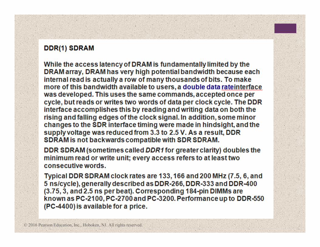
+Double Data Rate SDRAM
(DDR SDRAM)
� Developed by the JEDEC Solid State Technology Association
(Electronic Industries Alliance’s semiconductor-engineering-
standardization body)
� Numerous companies make DDR chips, which are widely
used in desktop computers and servers
� DDR achieves higher data rates in three ways:
� First, the data transfer is synchronized to both the rising and
falling edge of the clock, rather than just the rising edge
� Second, DDR uses higher clock rate on the bus to increase the
transfer rate
� Third, a buffering scheme is used
© 2016 Pearson Education, Inc., Hoboken, NJ. All rights reserved.
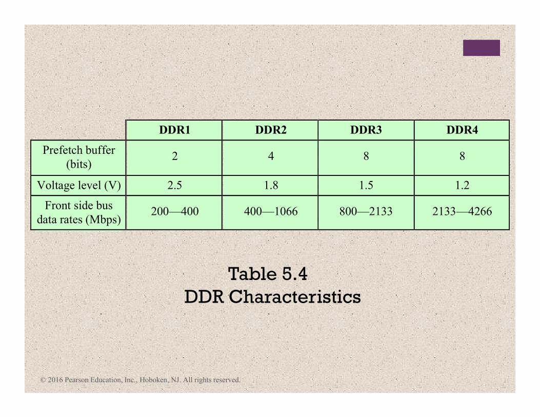
DDR1 DDR2 DDR3 DDR4
Prefetch buffer
(bits) 2 4 8 8
Voltage level (V) 2.5 1.8 1.5 1.2
Front side bus
data rates (Mbps) 200—400 400—1066 800—2133 2133—4266
Table 5.4
DDR Characteristics
© 2016 Pearson Education, Inc., Hoboken, NJ. All rights reserved.
© 2016 Pearson Education, Inc., Hoboken, NJ. All rights reserved.
© 2016 Pearson Education, Inc., Hoboken, NJ. All rights reserved.
© 2016 Pearson Education, Inc., Hoboken, NJ. All rights reserved.
© 2016 Pearson Education, Inc., Hoboken, NJ. All rights reserved.
© 2016 Pearson Education, Inc., Hoboken, NJ. All rights reserved.
© 2016 Pearson Education, Inc., Hoboken, NJ. All rights reserved.
+Flash Memory
� Used both for internal memory and external memory applications
� First introduced in the mid-1980’s
� Is intermediate between EPROM and EEPROM in both cost and functionality
� Uses an electrical erasing technology like EEPROM
� It is possible to erase just blocks of memory rather than an entire chip
� Gets its name because the microchip is organized so that a section of memory cells are erased in a single action
� Does not provide byte-level erasure
� Uses only one transistor per bit so it achieves the high density of EPROM
© 2016 Pearson Education, Inc., Hoboken, NJ. All rights reserved.
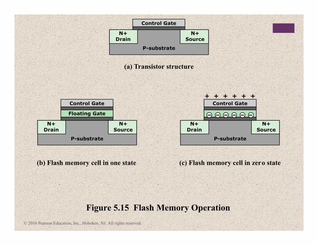
Figure 5.15 Flash Memory Operation
(a) Transistor structure
(b) Flash memory cell in one state (c) Flash memory cell in zero state
Control Gate
N+Drain
N+Source
P-substrate
Control Gate
N+Drain
N+Source
Floating Gate
P-substrate
Control Gate
+ + + + + +
N+Drain
N+Source
P-substrate
– – – – – –
© 2016 Pearson Education, Inc., Hoboken, NJ. All rights reserved.
© 2016 Pearson Education, Inc., Hoboken, NJ. All rights reserved.
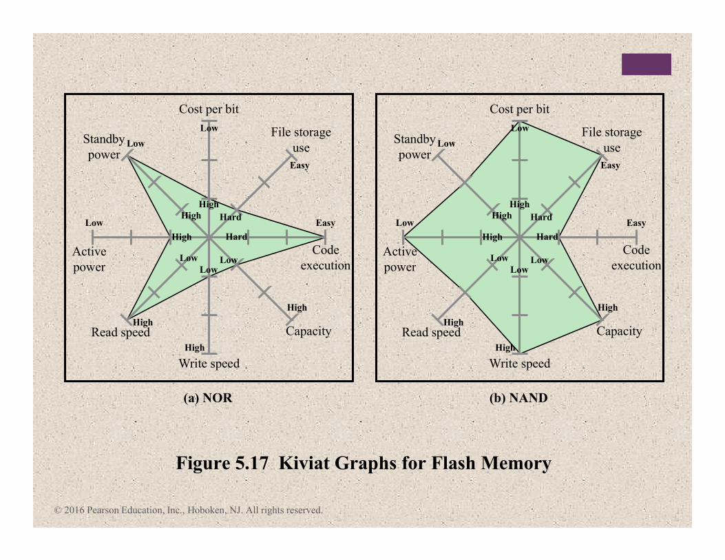
(a) NOR
Figure 5.17 Kiviat Graphs for Flash Memory
Cost per bit
File storage
use
Code
execution
Capacity
Write speed
Read speed
Active
power
Low
Low
Low
Easy
Easy
Standby
power
High
High
High
High
High
High
Hard
Hard
Low
LowLow
(b) NAND
Cost per bit
File storage
use
Code
execution
Capacity
Write speed
Read speed
Active
power
Low
Low
Low
Easy
Easy
Standby
power
High
High
High
High
High
High
Hard
Hard
Low
LowLow
© 2016 Pearson Education, Inc., Hoboken, NJ. All rights reserved.
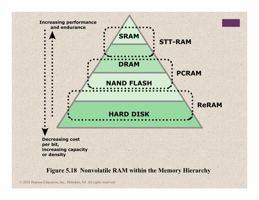
Figure 5.18 Nonvolatile RAM within the Memory Hierarchy
SRAMSTT-RAM
PCRAM
ReRAM
Increasing performanceand endurance
Decreasing costper bit,increasing capacityor density
DRAM
NAND FLASH
HARD DISK
© 2016 Pearson Education, Inc., Hoboken, NJ. All rights reserved.
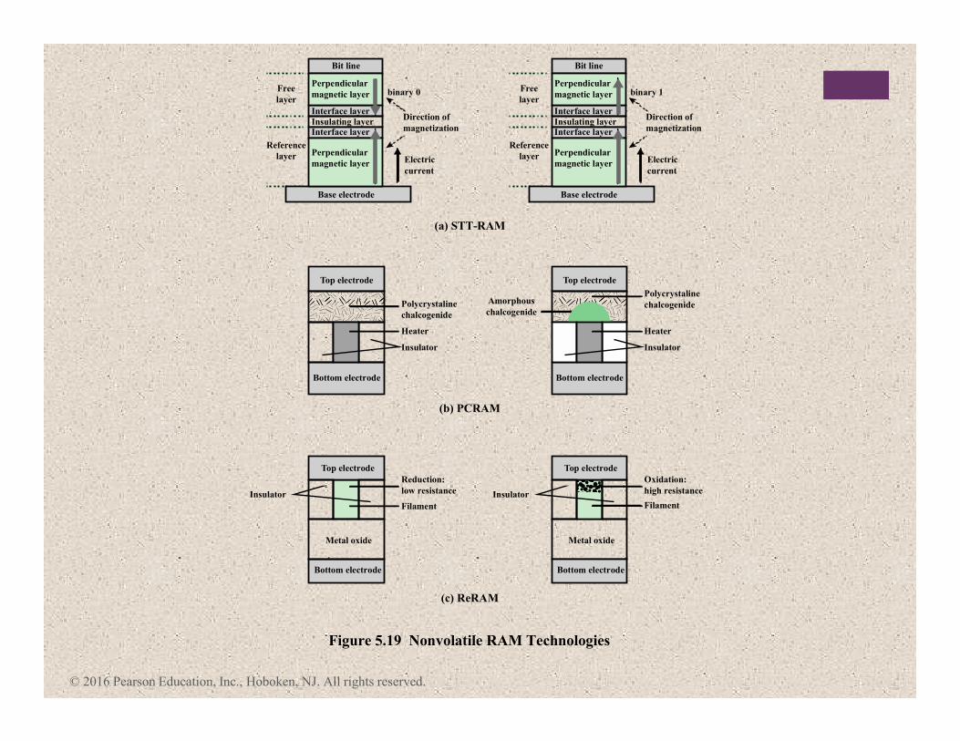
Figure 5.19 Nonvolatile RAM Technologies
(a) STT-RAM
(b) PCRAM
Bit line
Free
layer
Reference
layer
Base electrode
Interface layerDirection of
magnetization
Electric
current
binary 0
Interface layerInsulating layer
Perpendicular
magnetic layer
Perpendicular
magnetic layer
Bit line
Free
layer
Reference
layer
Base electrode
Interface layerDirection of
magnetization
Electric
current
binary 1
Interface layerInsulating layer
Perpendicular
magnetic layer
Perpendicular
magnetic layer
Top electrode
Bottom electrode
Polycrystaline
chalcogenide
Heater
Insulator
Filament
Metal oxide
Insulator
Metal oxide
Insulator
(c) ReRAM
Top electrode
Bottom electrode
Filament
Oxidation:
high resistance
Reduction:
low resistance
Top electrode
Bottom electrode
Top electrode
Bottom electrode
Polycrystaline
chalcogenideAmorphous
chalcogenide
Heater
Insulator
© 2016 Pearson Education, Inc., Hoboken, NJ. All rights reserved.
+ Summary
� Semiconductor main memory
� Organization
� DRAM and SRAM
� Types of ROM
� Chip logic
� Chip packaging
� Module organization
� Interleaved memory
� Error correction
� DDR DRAM
� Synchronous DRAM
� DDR SDRAM
� Flash memory
� Operation
� NOR and NAND flash memory
� Newer nonvolatile solid-state
memory technologies
Chapter 5
Internal
Memory
© 2016 Pearson Education, Inc., Hoboken, NJ. All rights reserved.