Embed Size (px)
Citation preview
www.tescan.comwww.witec.de
RISE MicroscopyCorrelative microscopy on a new level –Complementing ultra-structural SEM with molecular Raman imaging
Raman Imaging and Scanning Electron Microscopy
Materials science, nanotechnology, polymer science, geosciences, life science, pharmaceutical industry etc. … …regardless of the field in which you are working, RISE Microscopy will empower you with its unique imaging capabilities.
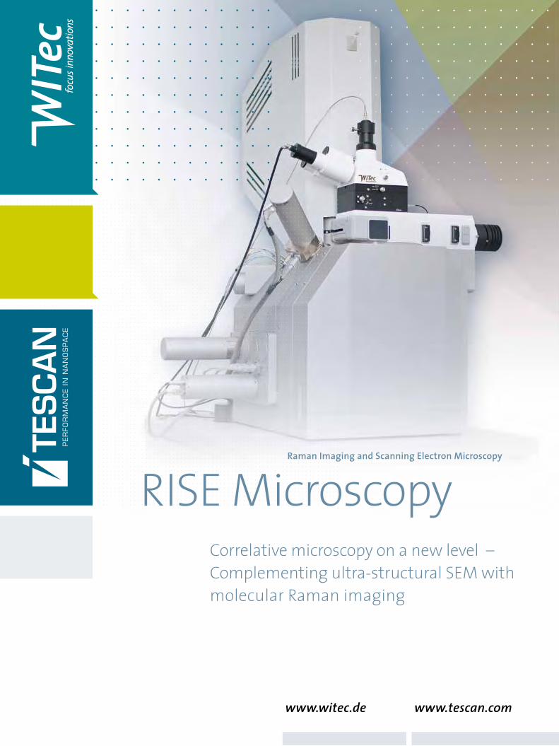
RISE Microscopy
World’s first fully-integrated Raman Imaging and Scanning Electron Microscope
>>>>
>>
Correlative Scanning Electron and confocal Raman Imaging for comprehensive sample analysis
A new dimension in imaging: ultra-structural SEM complemented with chemical compound information and molecular Raman imaging
RisE Microscopy is suitable for you……as a Raman newcomer you will benefit from the ease-of-use and intuitive measurement procedure
…as an experienced user you will appreciate the exceptional correlative microscope performance with the advantages of both techniques included in one instrument
ApplicAtions
carbon
plagioclase (feldspar)
plagioclase (feldspar)
apatite
RAMAnsEM sEM
a
SEM RAMAn-sEMRAMAN
a b c
b c
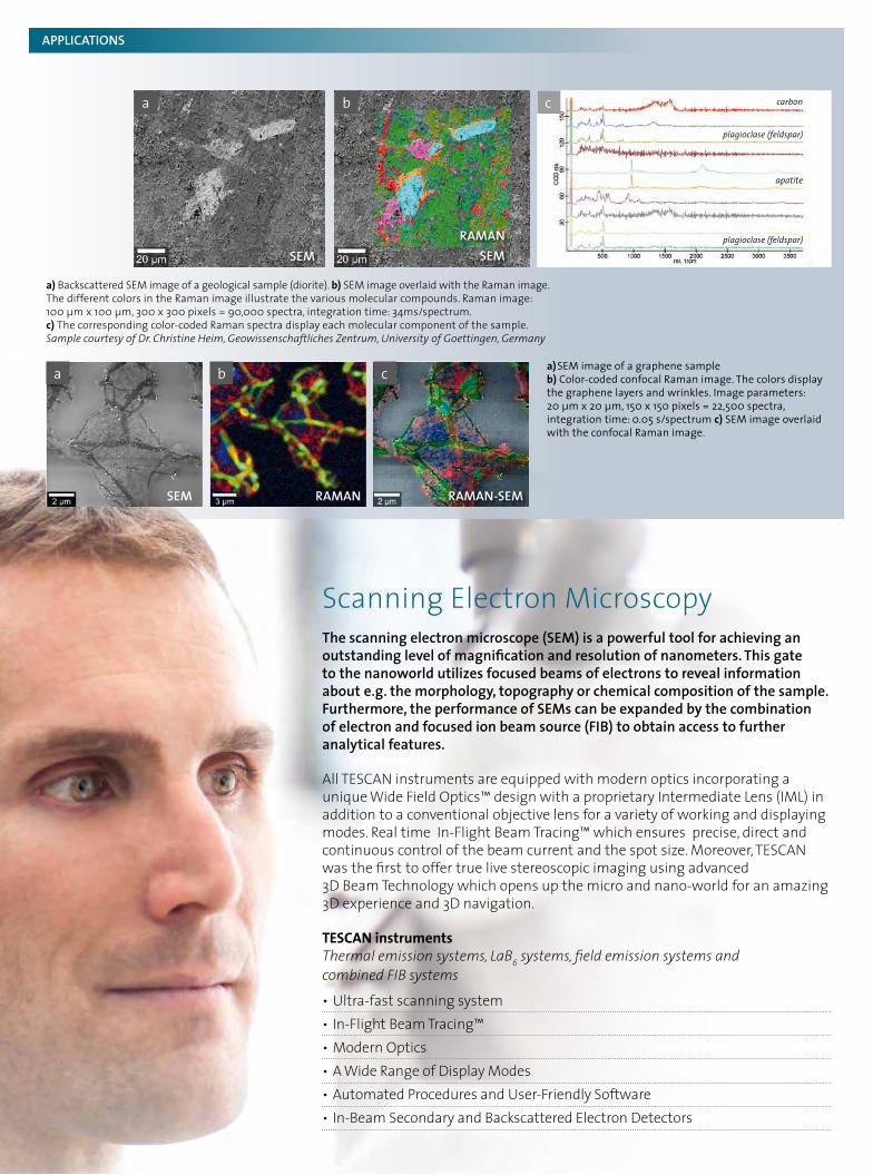
a) Backscattered SEM image of a geological sample (diorite). b) SEM image overlaid with the Raman image. The different colors in the Raman image illustrate the various molecular compounds. Raman image: 100 μm x 100 μm, 300 x 300 pixels = 90,000 spectra, integration time: 34ms/spectrum.c) The corresponding color-coded Raman spectra display each molecular component of the sample. Sample courtesy of Dr. Christine Heim, Geowissenschaftliches Zentrum, University of Goettingen, Germany
a)SEMimageofagraphenesampleb)Color-codedconfocalRamanimage.Thecolorsdisplaythegraphenelayersandwrinkles.Imageparameters:20μmx20μm,150x150pixels=22,500spectra,integrationtime:0.05s/spectrumc) SEMimageoverlaidwiththeconfocalRamanimage.
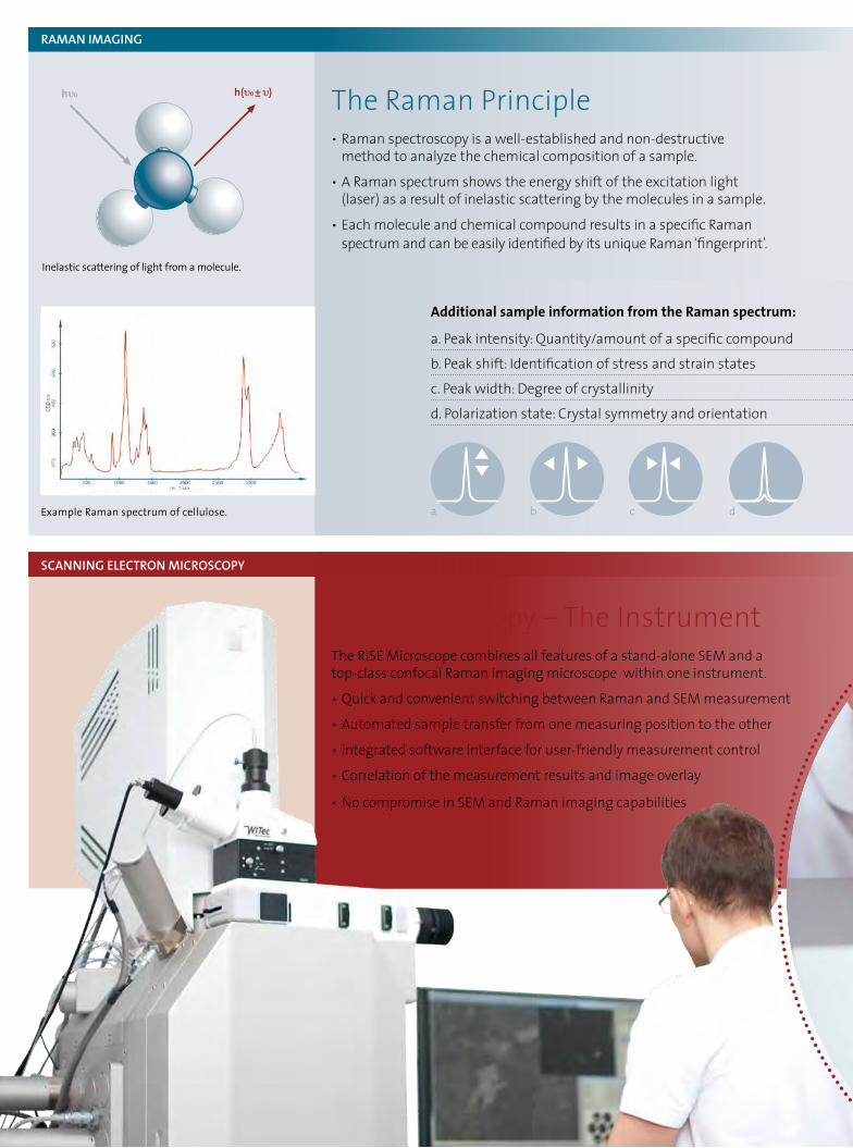
Scanning Electron Microscopythe scanning electron microscope (sEM) is a powerful tool for achieving an outstanding level of magnification and resolution of nanometers. this gate to the nanoworld utilizes focused beams of electrons to reveal information about e.g. the morphology, topography or chemical composition of the sample. Furthermore, the performance of sEMs can be expanded by the combination of electron and focused ion beam source (FiB) to obtain access to further analytical features.
All TESCAN instruments are equipped with modern optics incorporating a unique Wide Field Optics™ design with a proprietary Intermediate Lens (IML) in addition to a conventional objective lens for a variety of working and displaying modes. Real time In-Flight Beam Tracing™ which ensures precise, direct and continuous control of the beam current and the spot size. Moreover, TESCAN was the first to offer true live stereoscopic imaging using advanced 3D Beam Technology which opens up the micro and nano-world for an amazing 3D experience and 3D navigation.
TESCAN instruments Thermal emission systems, LaB6 systems, field emission systems and combined FIB systems
• Ultra-fast scanning system• In-Flight Beam Tracing™• Modern Optics• A Wide Range of Display Modes • Automated Procedures and User-Friendly Software• In-Beam Secondary and Backscattered Electron Detectors
RAMAn iMAGinG
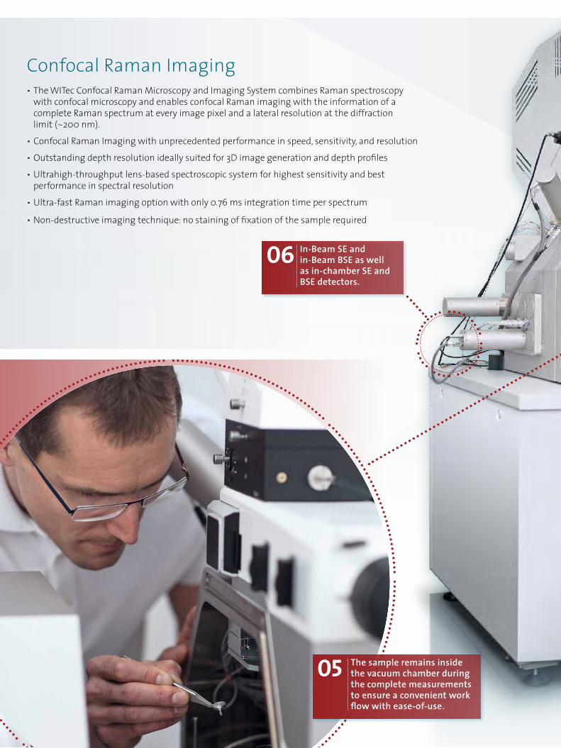
The Raman Principle• Raman spectroscopy is a well-established and non-destructive method to analyze the chemical composition of a sample.
• A Raman spectrum shows the energy shift of the excitation light (laser) as a result of inelastic scattering by the molecules in a sample.
• Each molecule and chemical compound results in a specific Raman spectrum and can be easily identified by its unique Raman ‘fingerprint’.
h�0 h(�0± �)
Inelasticscatteringoflightfromamolecule.
ExampleRamanspectrumofcellulose.
scAnninG ElEctRon MicRoscopY
Additional sample information from the Raman spectrum:
a. Peak intensity: Quantity/amount of a specific compound
b. Peak shift: Identification of stress and strain states
c. Peak width: Degree of crystallinity
d. Polarization state: Crystal symmetry and orientation
a b c d
RISE Microscopy – The InstrumentThe RISE Microscope combines all features of a stand-alone SEM and a top-class confocal Raman imaging microscope within one instrument.
• Quick and convenient switching between Raman and SEM measurement
• Automated sample transfer from one measuring position to the other
• Integrated software interface for user-friendly measurement control
• Correlation of the measurement results and image overlay
• No compromise in SEM and Raman imaging capabilities
in-Beam sE and in-Beam BsE as well as in-chamber sE and BsE detectors.
06
Confocal Raman Imaging• The WITec Confocal Raman Microscopy and Imaging System combines Raman spectroscopy
with confocal microscopy and enables confocal Raman imaging with the information of a complete Raman spectrum at every image pixel and a lateral resolution at the diffraction limit (~200 nm).
• Confocal Raman Imaging with unprecedented performance in speed, sensitivity, and resolution
• Outstanding depth resolution ideally suited for 3D image generation and depth profiles
• Ultrahigh-throughput lens-based spectroscopic system for highest sensitivity and best performance in spectral resolution
• Ultra-fast Raman imaging option with only 0.76 ms integration time per spectrum
• Non-destructive imaging technique: no staining of fixation of the sample required
the sample remains inside the vacuum chamber during the complete measurements to ensure a convenient work flow with ease-of-use.
05
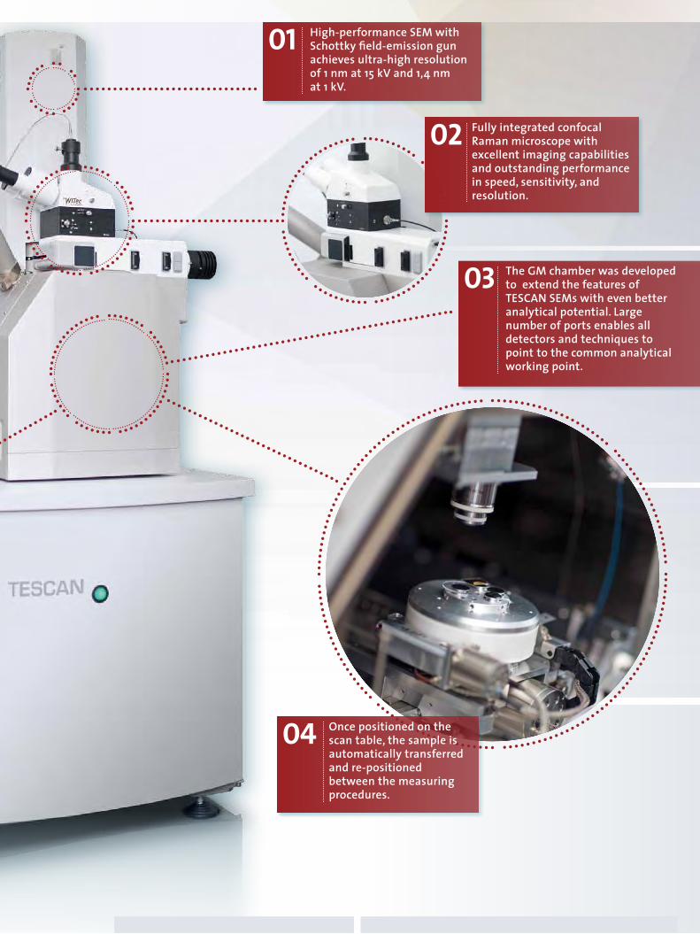
High-performance sEM with schottky field-emission gun achieves ultra-high resolution of 1 nm at 15 kV and 1,4 nm at 1 kV.
01
the GM chamber was developed to extend the features of tEscAn sEMs with even better analytical potential. large number of ports enables all detectors and techniques to point to the common analytical working point.
03
once positioned on the scan table, the sample is automatically transferred and re-positioned between the measuring procedures.
04
Fully integrated confocal Raman microscope with excellent imaging capabilities and outstanding performance in speed, sensitivity, and resolution.
02
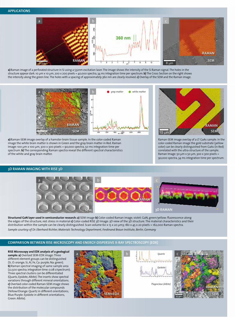
a)RamanimageofaperforatedstructureinSiusinga532nmexcitationlaser.TheimageshowstheintensityoftheSiRamansignal.Theholesinthestructureappeardark.10μmx10μm,200x200pixels=40,000spectra,34msintegrationtimeperspectrum.b)TheCrossSectionontherightshowstheintensityalongthegreenline.Theholeswithaspacingofapproximately360nmareclearlyresolved.c)OverlayoftheSEMandtheRamanimage.
Structured GaN layer used in semiconductor research: a)SEMimageb) Color-codedRamanimage,violet:GaN,green/yellow:fluorescencealongtheedgesofthestructure,red:stressinmaterialc)Color-codedRISE3DImage:3Dviewofthe3Dstructure.Thematerialcharacteristicsandtheirdistributionwithinthesamplecanbeclearlydistinguished.Scan-volume60x15x20μm3;180x45x20pixels=162,000Ramanspectra.Sample courtesy of Dr. Eberhard Richter, Materials Technology Department, Ferdinand Braun Institute, Berlin, Germany
a)Raman-SEMimageoverlayofahamsterbraintissuesample.Inthecolor-codedRamanimagethewhitebrainmatterisshowninGreenandthegraybrainmatterinRed.RamanImage:100μmx100μm,300x300pixels=90,000spectra,50msintegrationtimeperspectrum.b)ThecorrespondingRamanspectrarevealthedifferentspectralcharacteristicsofthewhiteandgraybrainmatter.
Raman-SEMimageoverlayofaLTGaAssample.Inthecolor-codedRamanimagethegoldsubstrate(yellowcolor)canbeclearlydistinguishedfromGaAs(inRed)correlatedwiththeultra-structureofthesample.RamanImage:50μmx50μm,300x300pixels=90,000spectra,34msintegrationtimeperspectrum.
3D RAMAn iMAGinG WitH RisE 3D
coMpARison BEtWEEn RisE MicRoscopY AnD EnERGY-DispERsiVE X-RAY spEctRoscopY (EDX)
ApplicAtions
RAMAn RAMAn
RAMAn
RAMAN
sEM
sEM
sEM+EDX
sEM
sEM
RISE Microscopy and EDX analysis of a geological sample: a) OverlaidSEM-EDXimage:Threedifferentelementgroupscanbedistinguished(Si,O:orange;Si,Al,Fe,Ca:purple;Na:green).b)Ramanspectralimagingofsamesamplearea(22,500spectra;integrationtime:0.08s/spectrum):Threespectralclusterscanbedifferentiated(Quartz,Epidote,Albite).Theinsertsshowspectralvariationsthroughdifferentmineralorientations.c)Overlaidcolor-codedRaman-SEMimageshowsthedistributionofthemolecularcompounds(Yellow/Orange:Quartzindifferentorientations;Blue/Purple:Epidoteindifferentorientations,Green:Albite).
gray matter white matter
RAMAn
3D Raman
a
a
a
a
b
b
b
c
c
Plagioclase (Albite)
Epidote
Quartz
sEM
c
RAMAn
b
TESCAN Brno, s.r.o.The leading provider of scientific instrumentation is well known for its innovation and openness to work with researchers and customizing applications to fit specific analytical needs. TESCAN’s product range includes thermal emission systems, LaB6 systems, field emission systems, FIB and Plasma FIB systems.
The TESCAN brand has, within 23 years of its existence, built a formidable reputation; 1600+ SEMs installed in over 60 countries are a testament to TESCAN´s first-class quality and proven technology.
TESCAN Brno, s.r.o. was established as subsidiary of a multi-national company TESCAN ORSAY HOLDING after the merger (2013) of Czech company TESCAN, a leading global supplier of SEMs and focused ion beam workstations, and the French company ORSAY PHYSICS, a world leader in customized Focused Ion Beam and Electron Beam technology.
WITec GmbHWITec is the leading German manufacturer of confocal and scanning-probe microscopes for state-of-the-art Raman, Atomic Force (AFM), and Scanning Near-Field Optical Microscopy (SNOM). WITec’s headquarters is located in Ulm, Germany, where all WITec products are developed and produced. Branch offices in USA, Japan, Singapore, and Spain ensure a worldwide sales and support network. From the company’s founding in 1997, WITec has been distinguished by its innovative product portfolio and a microscope design that enables combinations of the various imaging techniques within one system.
An example of the company’s breakthrough development is the world’s first integrated Raman-AFM microscope. To this day, WITec’s confocal microscopes are unrivaled in sensitivity, resolution and imaging capabilities. Significant innovation awards document WITec’s enduring success and innovative strength.
tEscAn HeadquartersTESCANBrno,s.r.o.Libusinatr.1.62300Brno–Kohoutovice.CzechRepublicPhone+420530353211.Fax+420530353415info@tescan.cz.www.tescan.com
Witec HeadquartersWITecGmbHLise-Meitner-Straße6.D-89081Ulm.GermanyPhone+49(0)731140700.Fax+49(0)[email protected]
WITecHeadquartersinUlm,Germany TESCANHeadquartersinBrno,CzechRepublic