Embed Size (px)
Citation preview
When (Low) Power Really MattersWhen (Low) Power Really Matters
Yogesh K. Ramadass, AnanthaGroup
Microsystems Technology Laboratory
OutlineOutline
Introduction
Voltage Scaling techniques
Challenges with Low voltage operation
System Examples
Conclusion
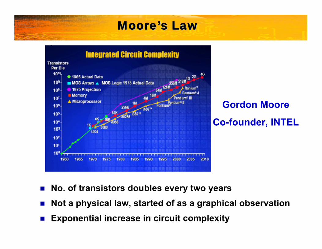
MooreMoore’’s Laws Law
No. of transistors doubles every two yearsNot a physical law, started of as a graphical observationExponential increase in circuit complexity
Gordon Moore
Co-founder, INTEL
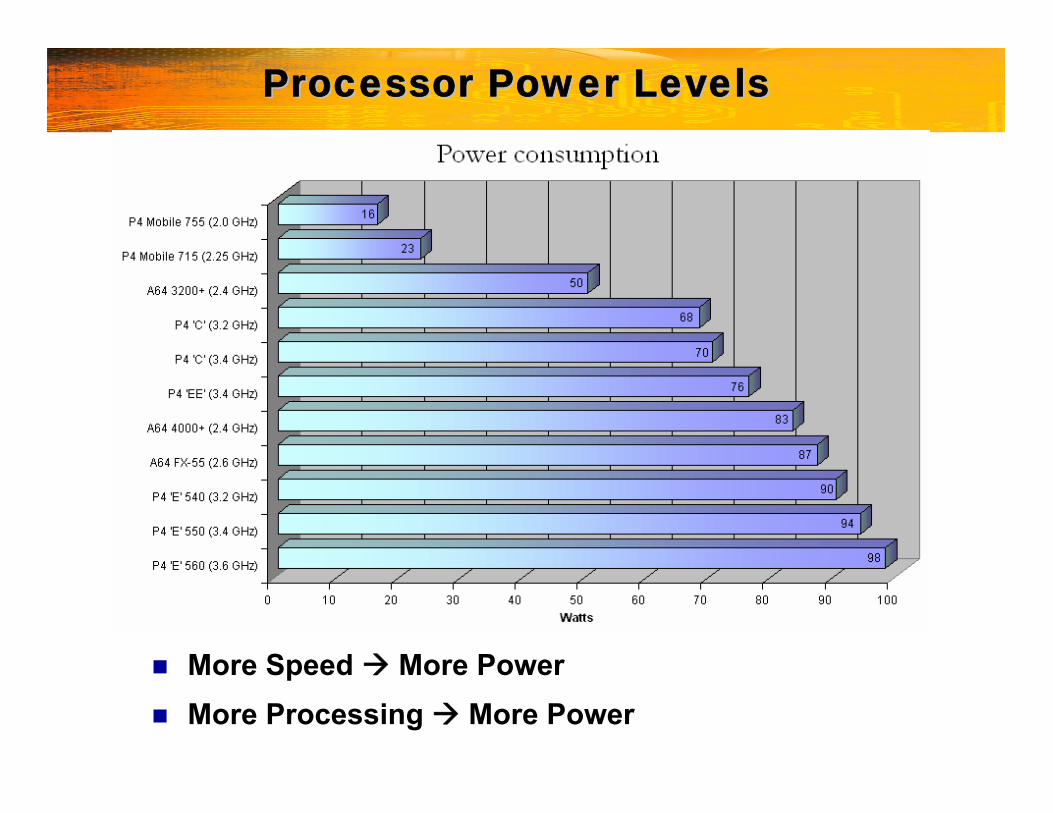
Processor Power LevelsProcessor Power Levels
More Speed More PowerMore Processing More Power
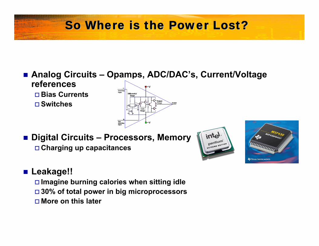
So Where is the Power Lost?So Where is the Power Lost?
Analog Circuits – Opamps, ADC/DAC’s, Current/Voltage references
Bias CurrentsSwitches
Digital Circuits – Processors, Memory Charging up capacitances
Leakage!!Imagine burning calories when sitting idle30% of total power in big microprocessorsMore on this later
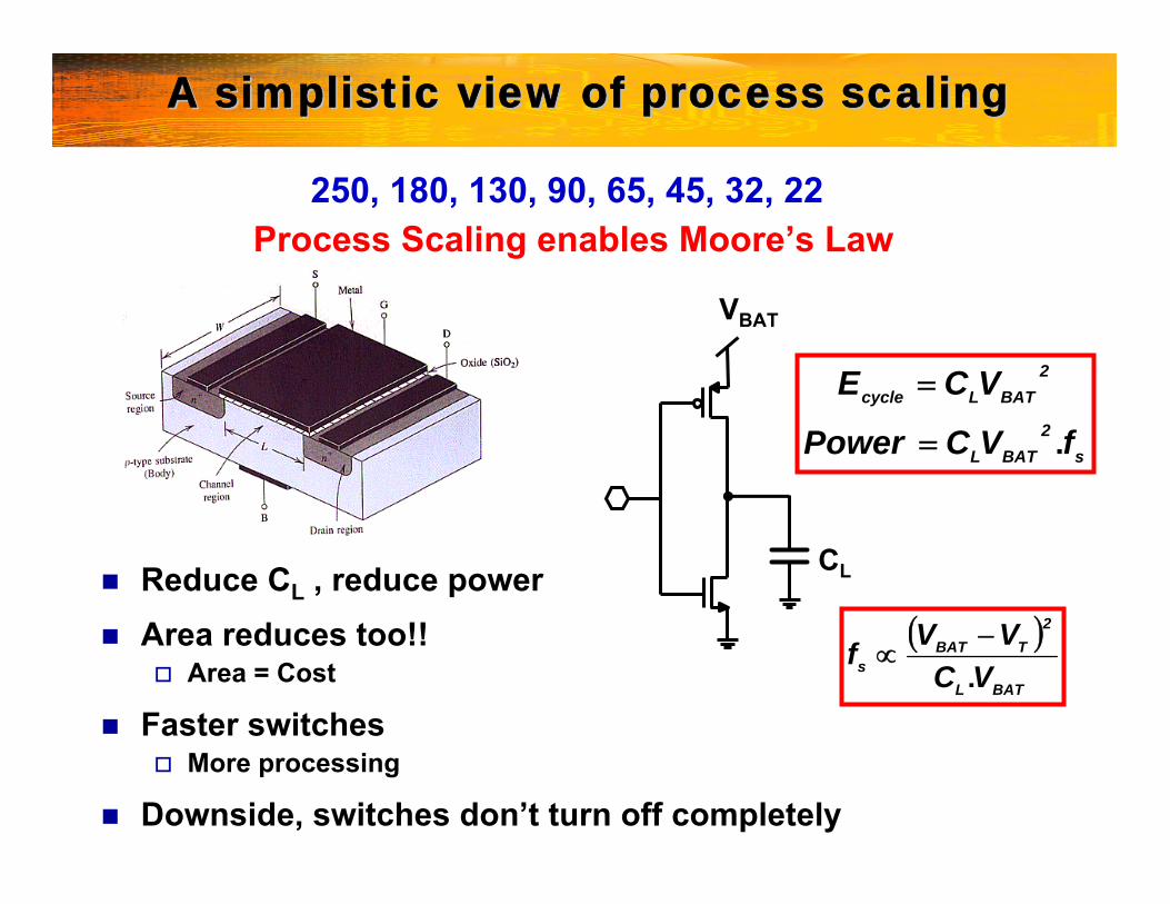
A simplistic view of process scalingA simplistic view of process scaling
VBAT
CLReduce CL , reduce powerArea reduces too!!
Area = Cost
Faster switchesMore processing
Downside, switches don’t turn off completely
250, 180, 130, 90, 65, 45, 32, 22Process Scaling enables Moore’s Law
s2
BATL
2BATLcycle
fVCPower
VCE
.=
=
( )BATL
2TBAT
s VCVVf
.−
∝
OutlineOutline
Introduction
Voltage Scaling techniques
Challenges with Low voltage operation
System Examples
Conclusion
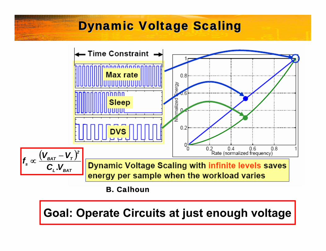
Dynamic Voltage ScalingDynamic Voltage Scaling
Goal: Operate Circuits at just enough voltage
B. Calhoun
( )BATL
2TBAT
s VCVVf
.−
∝
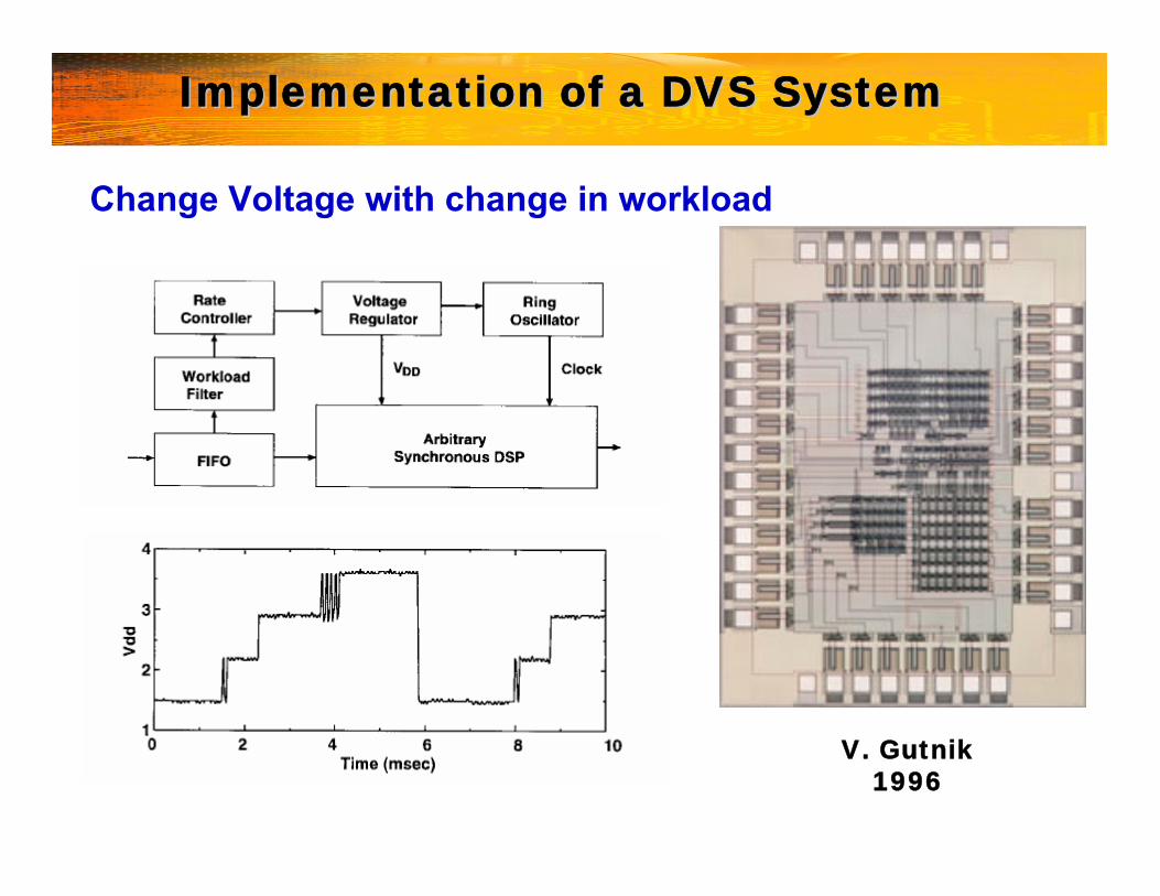
Implementation of a DVS SystemImplementation of a DVS System
V. Gutnik1996
Change Voltage with change in workload
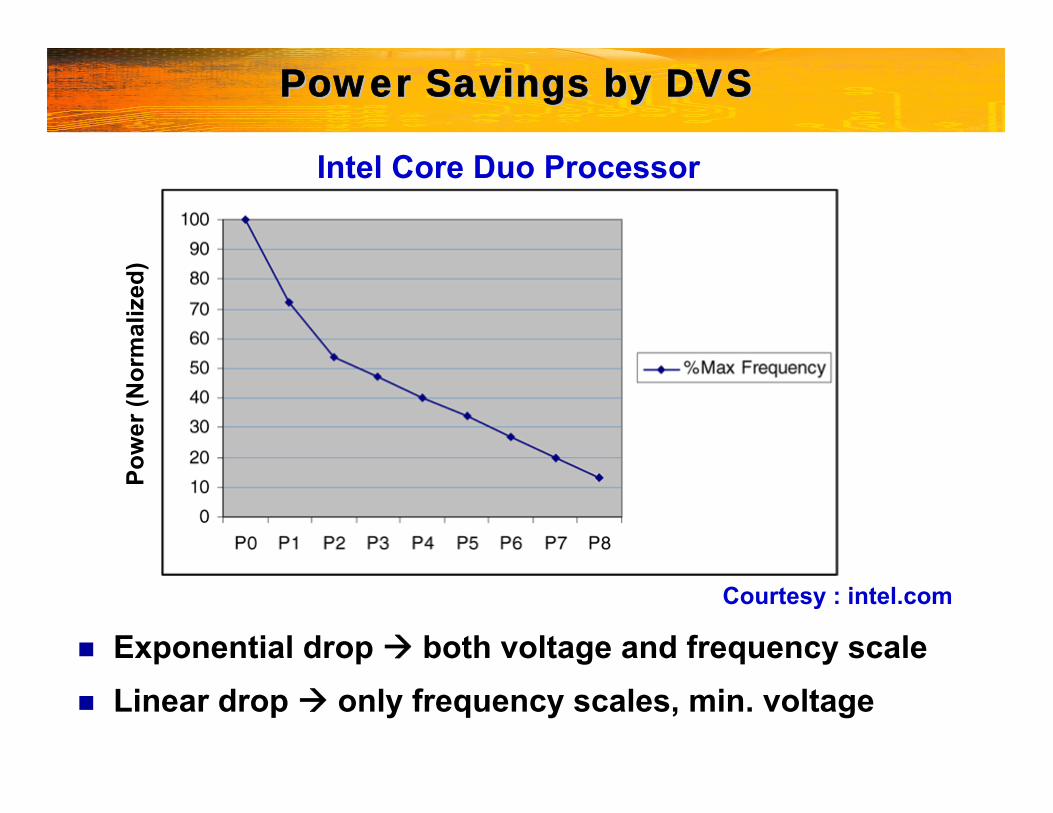
Power Savings by DVSPower Savings by DVS
Courtesy : intel.com
Exponential drop both voltage and frequency scaleLinear drop only frequency scales, min. voltage
Pow
er (N
orm
aliz
ed)
Intel Core Duo Processor
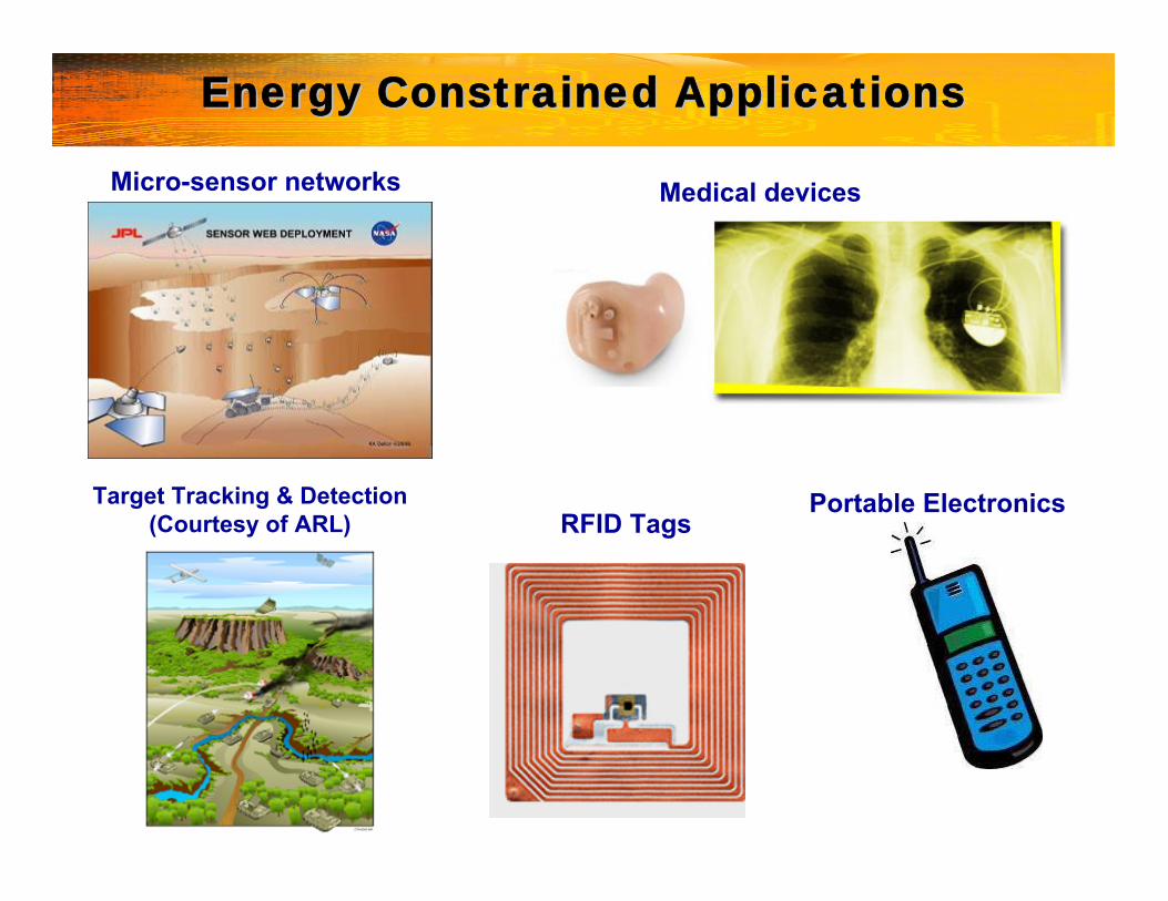
Energy Constrained ApplicationsEnergy Constrained Applications
Micro-sensor networks
RFID Tags
Medical devices
Portable ElectronicsTarget Tracking & Detection(Courtesy of ARL)
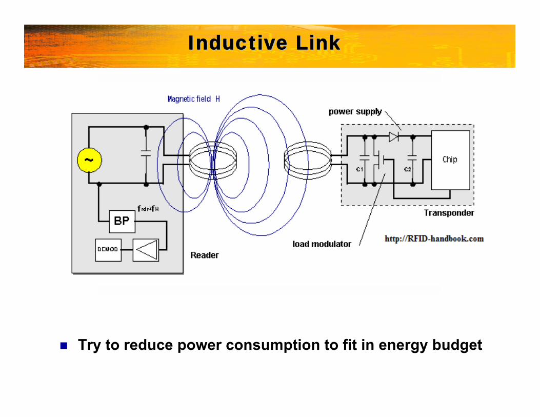
Inductive LinkInductive Link
Try to reduce power consumption to fit in energy budget
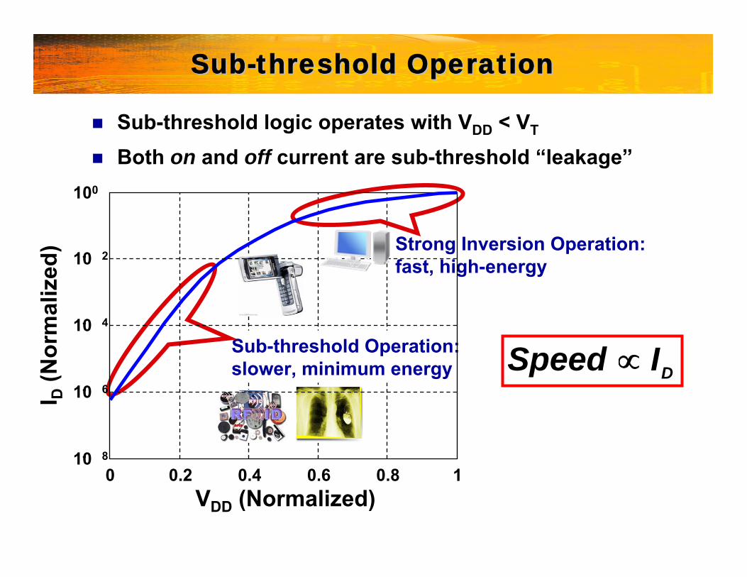
Sub-threshold Operation: slower, minimum energy
Strong Inversion Operation:fast, high-energy
0 0.2 0.4 0.6 0.8 110- 8
10- 6
10- 4
10- 2
100
VDD (Normalized)
I D(N
orm
aliz
ed)
Sub-threshold logic operates with VDD < VT
Both on and off current are sub-threshold “leakage”
SubSub--threshold Operationthreshold Operation
DISpeed ∝
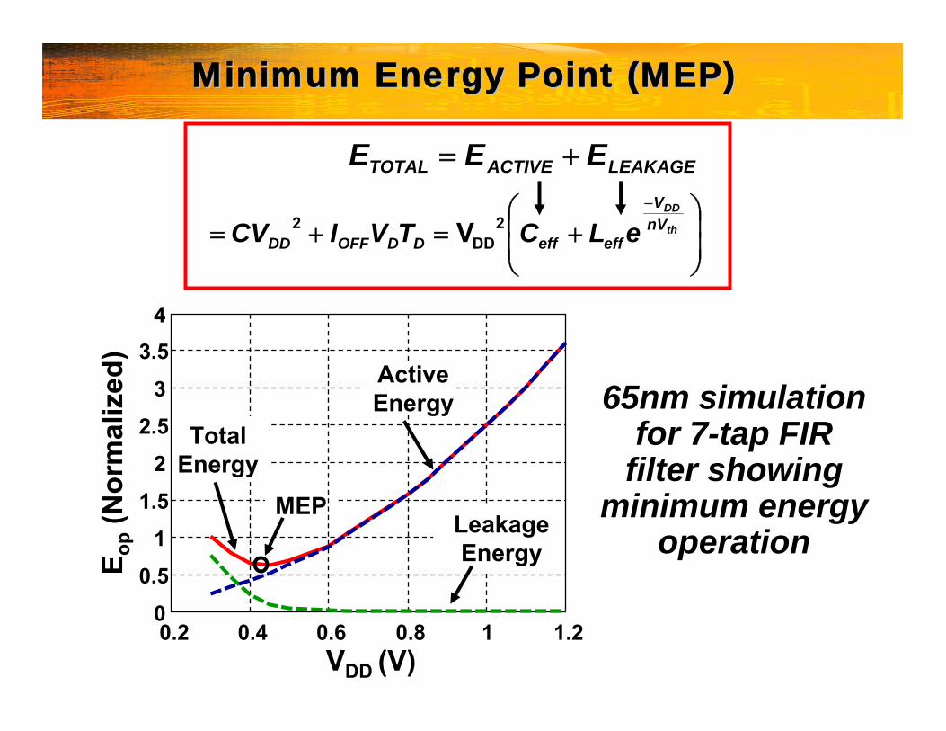
Minimum Energy Point (MEP)Minimum Energy Point (MEP)
LEAKAGEACTIVETOTAL EEE +=
⎟⎟⎠
⎞⎜⎜⎝
⎛+=+=
−
th
DDnVV
effeffDDOFFDD eLCTVICV 2DD
2 V
65nm simulation for 7-tap FIR
filter showing minimum energy
operationLeakage Energy
Total Energy
Active Energy
MEP
0.2 0.4 0.6 0.8 1 1.20
0.5
1
1.5
2
2.5
3
3.54
VDD (V)
E op
(Nor
mal
ized
)
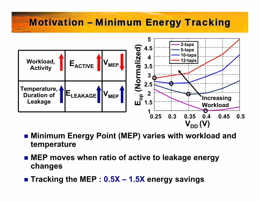
Motivation Motivation –– Minimum Energy TrackingMinimum Energy Tracking
Minimum Energy Point (MEP) varies with workload and temperatureMEP moves when ratio of active to leakage energy changes Tracking the MEP : 0.5X – 1.5X energy savings
Increasing Workload
0.25 0.3 0.35 0.4 0.45 0.51
1.52
2.53
3.54
4.55
2-taps5-taps10-taps12-taps
VDD (V)
E op
(Nor
mal
ized
)
Temperature, Duration of
LeakageELEAKAGE
VMEPEACTIVEWorkload,
Activity
VMEP
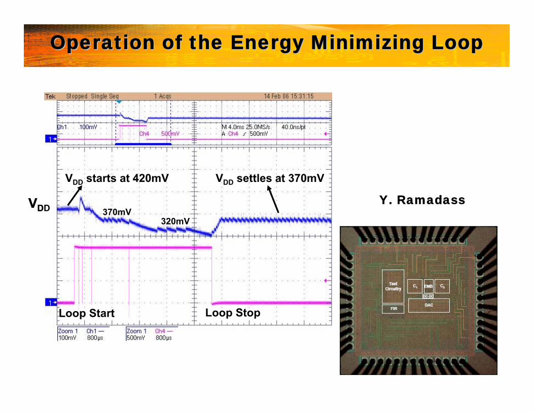
Operation of the Energy Minimizing LoopOperation of the Energy Minimizing Loop
VDD
Loop Start Loop Stop
VDD starts at 420mV VDD settles at 370mV
370mV320mV
VDD
Loop Start Loop Stop
VDD starts at 420mV VDD settles at 370mV
370mV320mV
Y. Ramadass
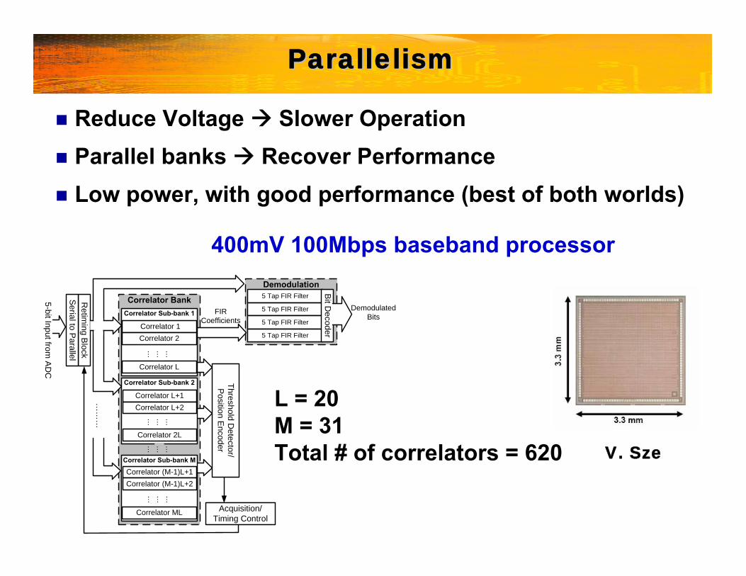
ParallelismParallelism
Correlator Bank
Demodulation
Correlator Sub-bank 1
Correlator 1Correlator 2
Correlator L
Correlator Sub-bank 2
Retim
ing Block
5 Tap FIR Filter
5 Tap FIR Filter
5 Tap FIR Filter
5 Tap FIR Filter
………
……
…
Correlator L+1Correlator L+2
Correlator 2L
Correlator Sub-bank M
Correlator (M-1)L+1Correlator (M-1)L+2
Correlator ML
5-bit Input from A
DC
Serial to P
arallel
Threshold Detector/
Position E
ncoder
Bit D
ecoder
………
………
………
DemodulatedBits
Acquisition/Timing Control
FIRCoefficients
L = 20M = 31Total # of correlators = 620 V. Sze
Reduce Voltage Slower OperationParallel banks Recover PerformanceLow power, with good performance (best of both worlds)
400mV 100Mbps baseband processor
OutlineOutline
Introduction
Voltage Scaling techniques
Challenges with Low voltage operation
System Examples
Conclusion
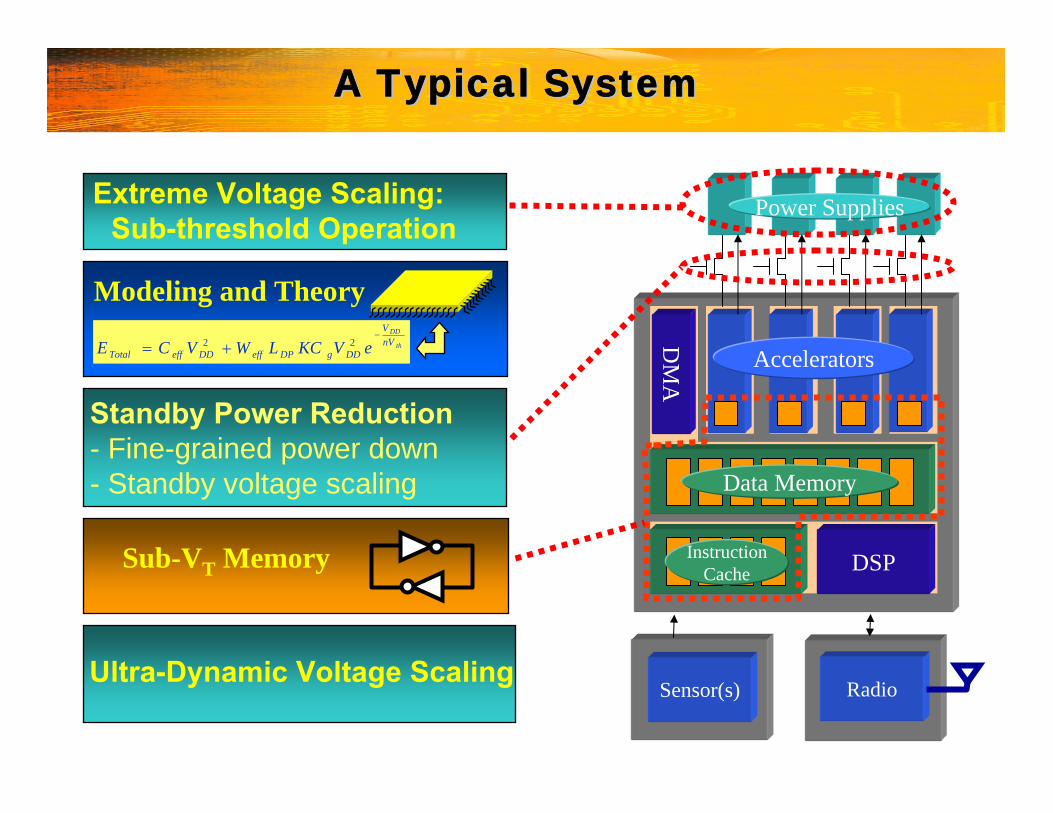
A Typical SystemA Typical System
DSP
DM
AAccelerators
Power Supplies
Data Memory
InstructionCache
Extreme Voltage Scaling: Sub-threshold Operation
Standby Power Reduction - Fine-grained power down- Standby voltage scaling
Sensor(s) Radio
Sub-VT Memory
Modeling and Theoryth
DDnVV
DDgDPeffDDeffTotal eVKCLWVCE−
+= 22
Ultra-Dynamic Voltage Scaling
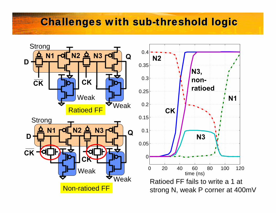
Challenges with subChallenges with sub--threshold logicthreshold logic
WeakWeak 0 20 40 60 80 100 120
0
0.05
0.1
0.15
0.2
0.25
0.3
0.35
0.4
time (ns)
Ratioed FF
Non-ratioed FF
WeakWeak
Strong
Strong
N1 N2 N3
N1 N2 N3
N1
N2
N3
N3, non-ratioed
CK
CK
CK
CK
CK
DQ
D Q
Ratioed FF fails to write a 1 atstrong N, weak P corner at 400mV
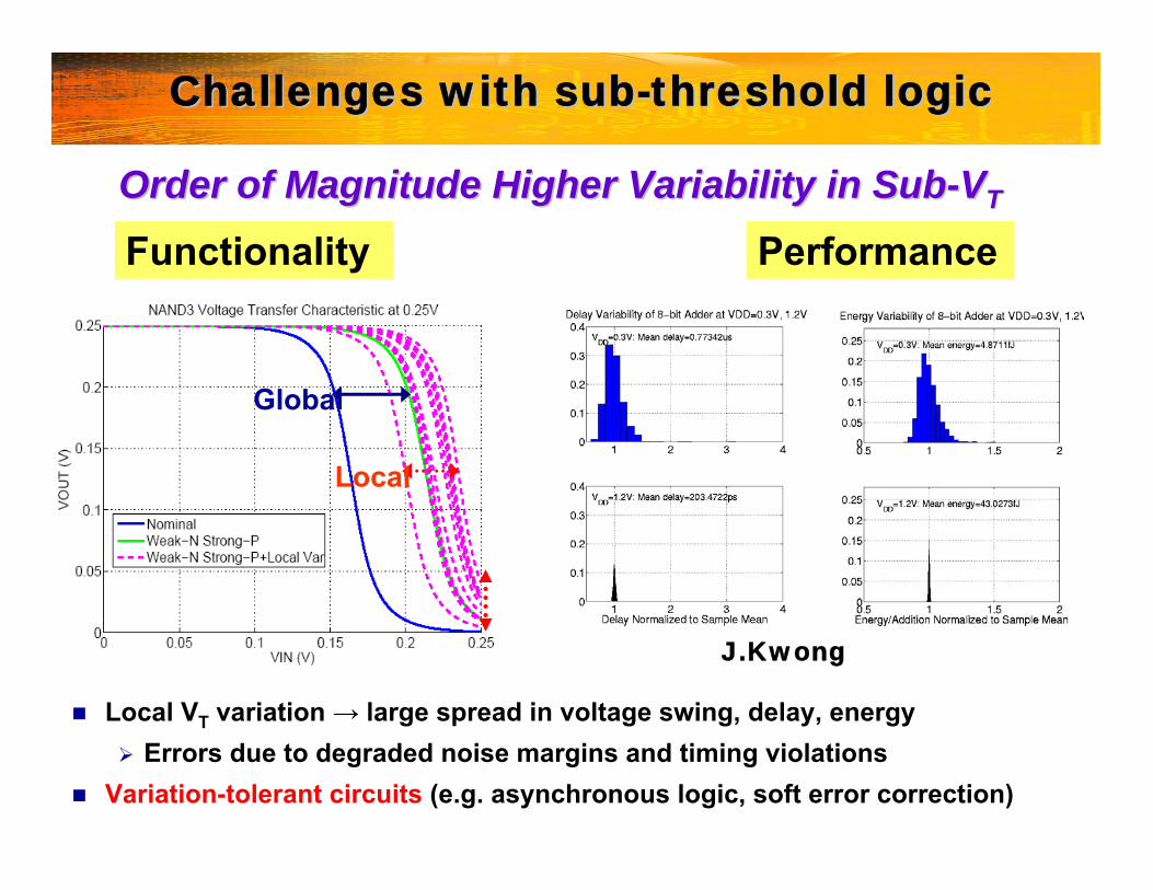
PerformanceOrder of Magnitude Higher Variability in SubOrder of Magnitude Higher Variability in Sub--VVTT
Global
Local
Functionality
Local VT variation → large spread in voltage swing, delay, energyErrors due to degraded noise margins and timing violations
Variation-tolerant circuits (e.g. asynchronous logic, soft error correction)
Challenges with subChallenges with sub--threshold logicthreshold logic
J.Kwong
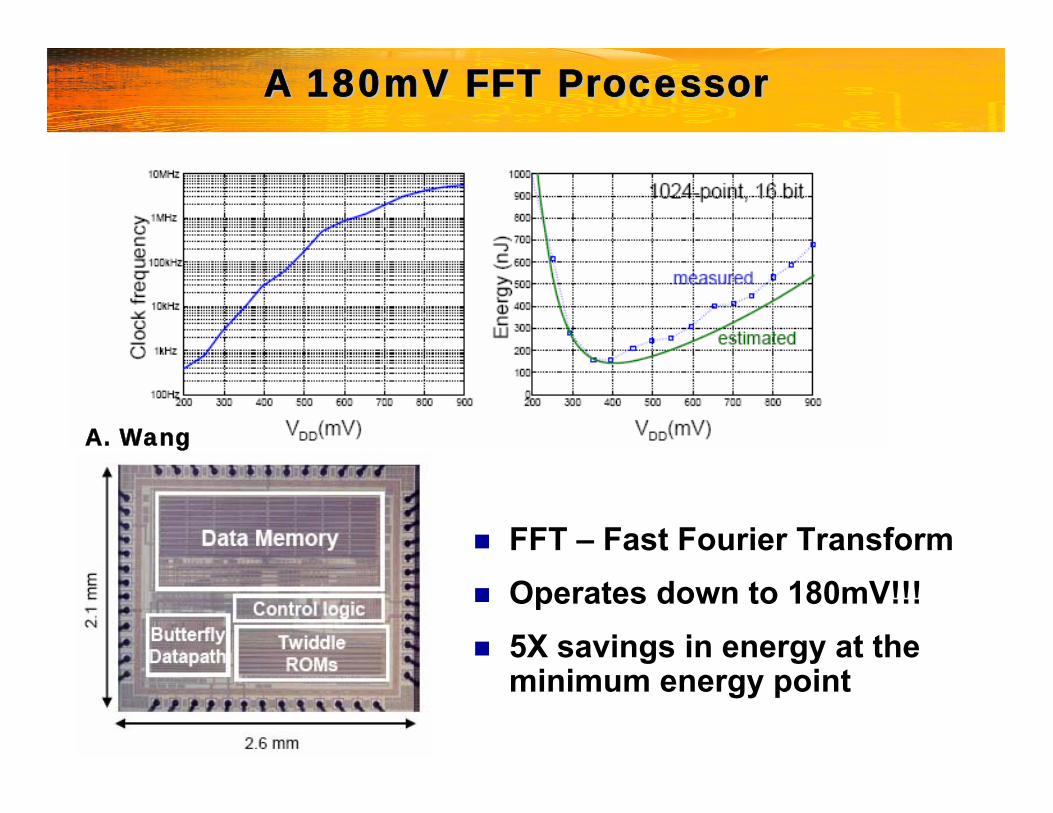
A 180mV FFT ProcessorA 180mV FFT Processor
FFT – Fast Fourier TransformOperates down to 180mV!!!5X savings in energy at the minimum energy point
A. Wang
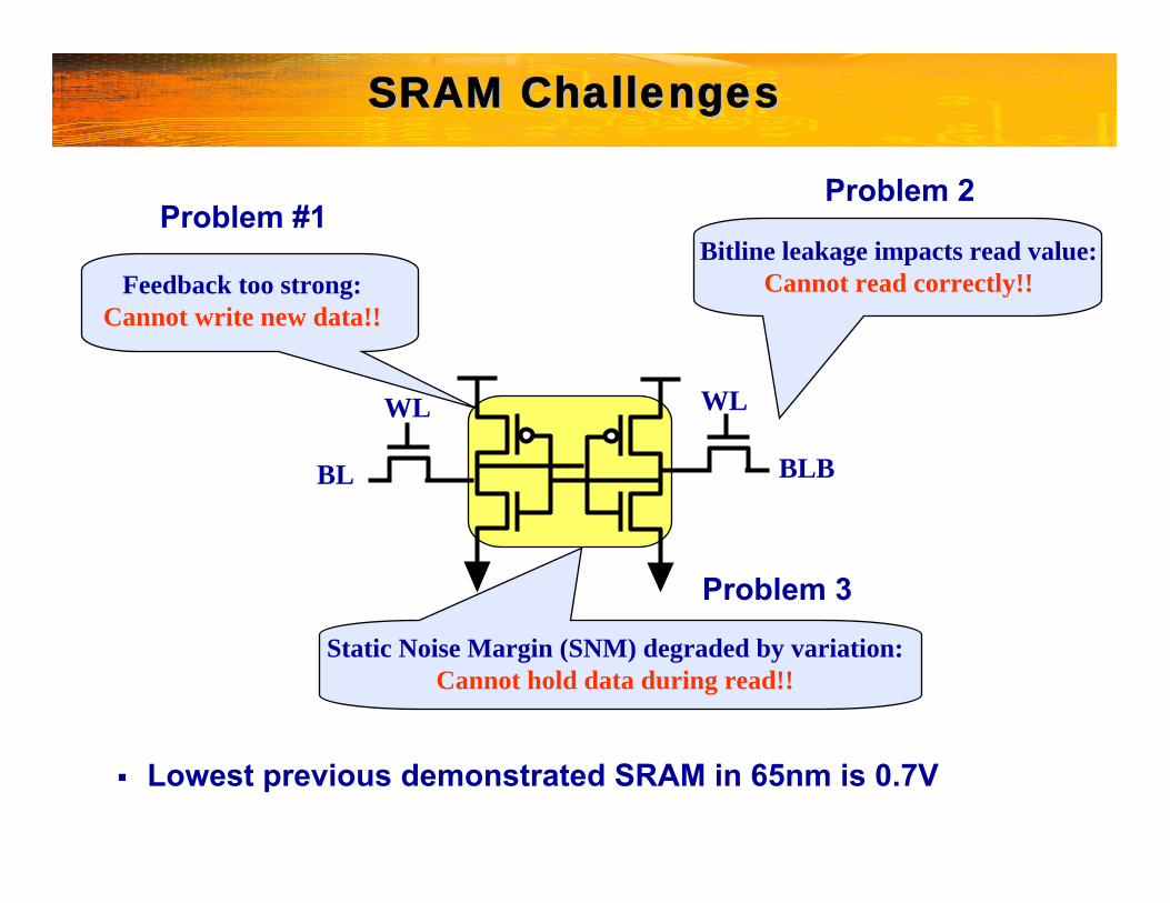
SRAM ChallengesSRAM Challenges
WL
BL BLB
WL
Static Noise Margin (SNM) degraded by variation:Cannot hold data during read!!
Feedback too strong:Cannot write new data!!
Bitline leakage impacts read value:Cannot read correctly!!
Lowest previous demonstrated SRAM in 65nm is 0.7V
Problem #1Problem 2
Problem 3
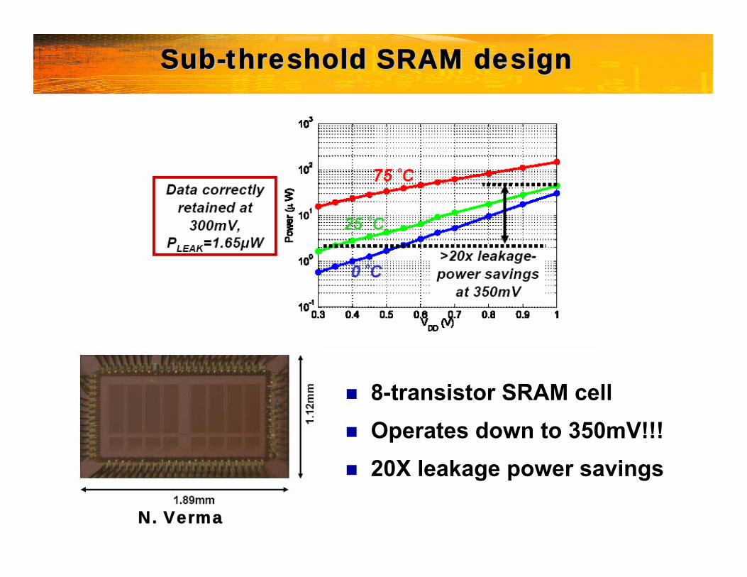
SubSub--threshold SRAM designthreshold SRAM design
N. Verma
8-transistor SRAM cellOperates down to 350mV!!!20X leakage power savings
OutlineOutline
Introduction
Voltage Scaling techniques
Challenges with Low voltage operation
System Examples
Conclusion
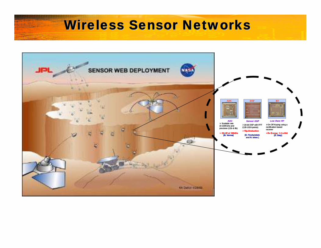
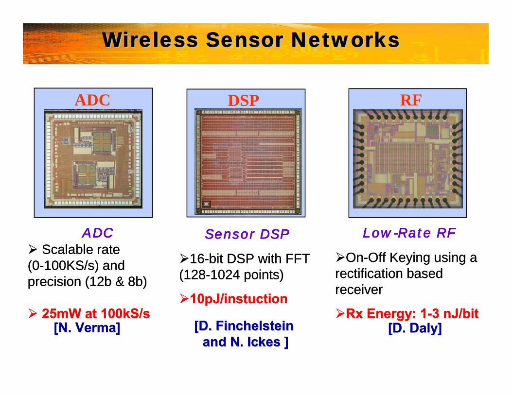
Wireless Sensor NetworksWireless Sensor Networks
ADCScalable rate
(0-100KS/s) and precision (12b & 8b)
25mW at 100kS/s
ADC DSP RF
Low-Rate RF
On-Off Keying using a rectification based receiver
Rx Energy: 1-3 nJ/bit[N. Verma] [D. Daly]
Sensor DSP
16-bit DSP with FFT (128-1024 points)
10pJ/instuction
[D. Finchelstein D. Finchelstein and N. Ickesand N. Ickes ]
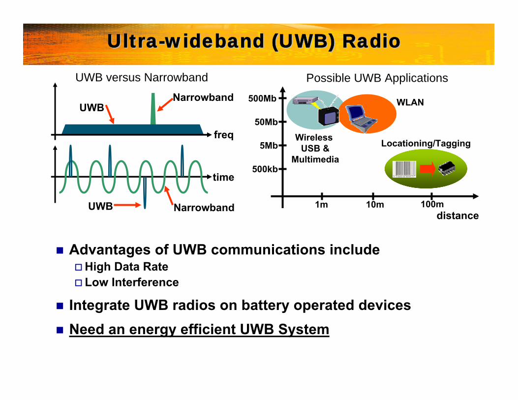
UltraUltra--wideband (UWB) Radiowideband (UWB) Radio
distance1m 10m 100m
500Mb
50Mb
5Mb
500kb
WLAN
Wireless USB &
Multimedia
Locationing/Tagging
Advantages of UWB communications includeHigh Data RateLow Interference
Integrate UWB radios on battery operated devicesNeed an energy efficient UWB System
Narrowband
Narrowband
UWB
UWB
Possible UWB ApplicationsUWB versus Narrowband
freq
time
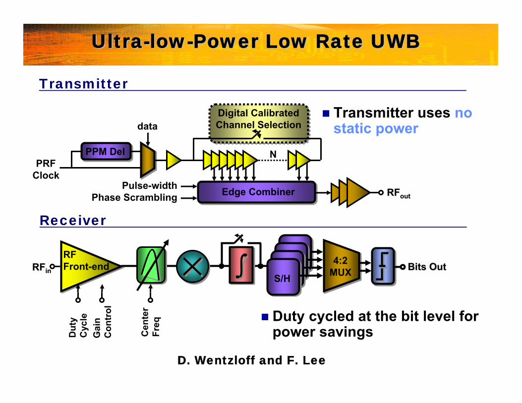
UltraUltra--lowlow--Power Low Rate UWBPower Low Rate UWB
S/HS/HS/HS/H
4:2MUX
RF Front-end Bits OutBits OutRFRFinin
Cen
ter
Freq
Gai
n C
ontr
ol
Dut
yC
ycle
Transmitter
Receiver
Edge Combiner
N
Digital CalibratedChannel Selection
PPM Del
data
PRFClock
RFRFoutoutPulse-width
Phase Scrambling
Transmitter uses no static power
Duty cycled at the bit level for power savings
D. Wentzloff and F. Lee
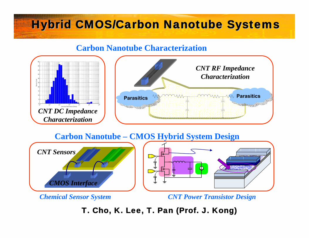
Hybrid CMOS/Carbon Hybrid CMOS/Carbon NanotubeNanotube Systems Systems
Carbon Nanotube Characterization
CNT DC Impedance Characterization
Chemical Sensor System
CNT Sensors
CMOS Interface
ParasiticsParasitics ParasiticsParasitics
CNT RF Impedance Characterization
Carbon Nanotube – CMOS Hybrid System Design
CNT Power Transistor Design
T. Cho, K. Lee, T. Pan (Prof. J. Kong)
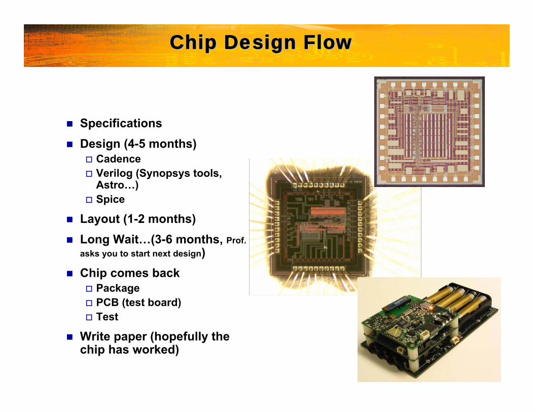
Chip Design FlowChip Design Flow
SpecificationsDesign (4-5 months)
CadenceVerilog (Synopsys tools, Astro…)Spice
Layout (1-2 months)Long Wait…(3-6 months, Prof. asks you to start next design)Chip comes back
PackagePCB (test board)Test
Write paper (hopefully the chip has worked)
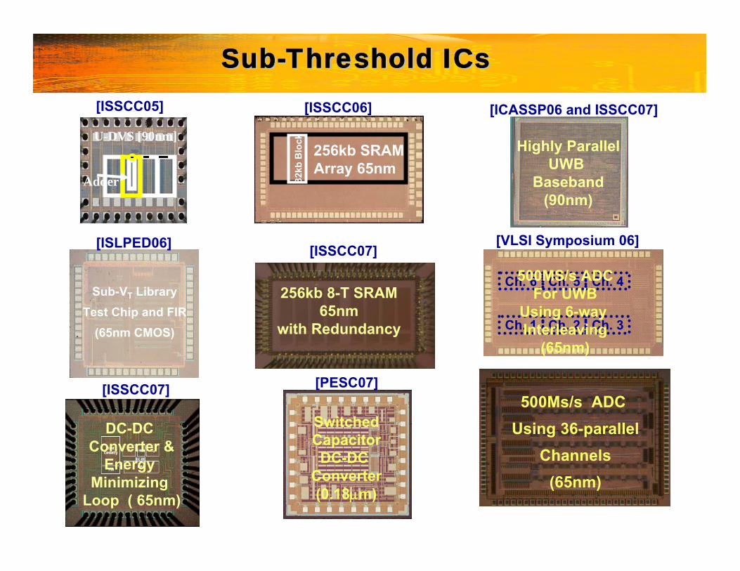
SubSub--Threshold ICsThreshold ICs
Sub-VT LibraryTest Chip and FIR
(65nm CMOS)
256kb 8-T SRAM65nm
with Redundancy
256kb SRAM Array 65nm
32kb
Blo
ck
DC-DC Converter &
Energy Minimizing
Loop ( 65nm)
Highly ParallelUWB
Baseband(90nm)
Ch. 6 Ch. 5 Ch. 4
Ch. 1 Ch. 2 Ch. 3
500MS/s ADCFor UWB
Using 6-way Interleaving
(65nm)
500Ms/s ADC Using 36-parallel
Channels(65nm)
SwitchedCapacitorDC-DC
Converter(0.18µm)
[ISLPED06]
[ISSCC06]
[ISSCC07]
[ISSCC07]
[ICASSP06 and ISSCC07]
[VLSI Symposium 06]
[PESC07]
U-DVS [90nm]
Adder
[ISSCC05]
Helpful ClassesHelpful Classes
Circuits – 6.002, 6.301, 6.374, 6.376, 6.775, 6.776, 6.334
Devices – 6.012, 6.728, 6.730, 6.774
Control Theory – 6.302, 6.331
Signal/Image Processing – 6.003, 6.341, 6.344
Communication – 6.450, 6.451

Groups at MITGroups at MIT
Circuit Design
Prof. Anantha Chandrakasan
Prof. Joel Dawson
Prof. Hae-Seung Lee
Prof. David Perreault
Prof. Michael Perrott
Prof. Rahul Sarpeshkar
Prof. Charles Sodini
Prof. Vladimir Stojanovic
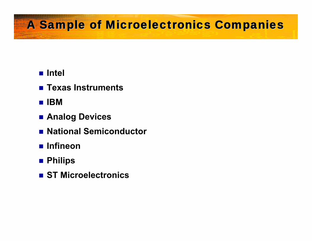
A Sample of Microelectronics CompaniesA Sample of Microelectronics Companies
IntelTexas InstrumentsIBMAnalog DevicesNational SemiconductorInfineonPhilipsST Microelectronics
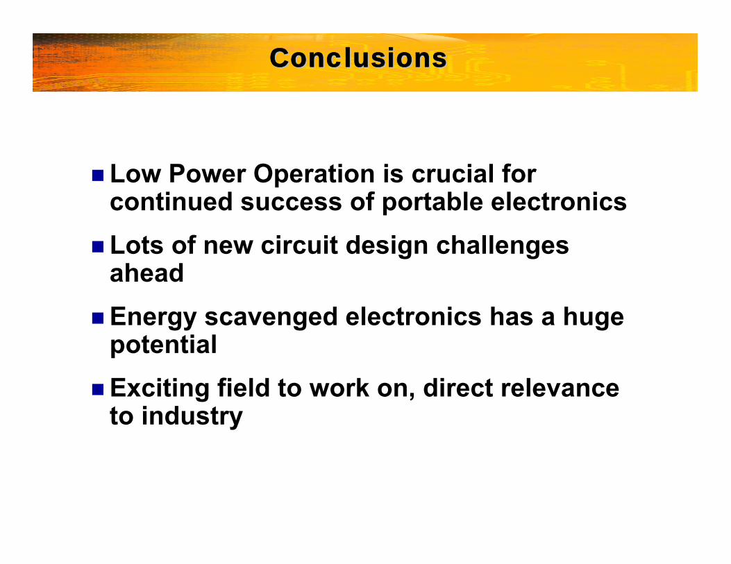
ConclusionsConclusions
Low Power Operation is crucial for continued success of portable electronicsLots of new circuit design challenges ahead Energy scavenged electronics has a huge potentialExciting field to work on, direct relevance to industry