Embed Size (px)
Citation preview

To learn more about ON Semiconductor, please visit our website at www.onsemi.com
Please note: As part of the Fairchild Semiconductor integration, some of the Fairchild orderable part numbers will need to change in order to meet ON Semiconductor’s system requirements. Since the ON Semiconductor product management systems do not have the ability to manage part nomenclature that utilizes an underscore (_), the underscore (_) in the Fairchild part numbers will be changed to a dash (-). This document may contain device numbers with an underscore (_). Please check the ON Semiconductor website to verify the updated device numbers. The most current and up-to-date ordering information can be found at www.onsemi.com. Please email any questions regarding the system integration to [email protected].
Is Now Part of
ON Semiconductor and the ON Semiconductor logo are trademarks of Semiconductor Components Industries, LLC dba ON Semiconductor or its subsidiaries in the United States and/or other countries. ON Semiconductor owns the rights to a number of patents, trademarks, copyrights, trade secrets, and other intellectual property. A listing of ON Semiconductor’s product/patent coverage may be accessed at www.onsemi.com/site/pdf/Patent-Marking.pdf. ON Semiconductor reserves the right to make changes without further notice to any products herein. ON Semiconductor makes no warranty, representation or guarantee regarding the suitability of its products for any particular purpose, nor does ON Semiconductor assume any liability arising out of the application or use of any product or circuit, and specifically disclaims any and all liability, including without limitation special, consequential or incidental damages. Buyer is responsible for its products and applications using ON Semiconductor products, including compliance with all laws, regulations and safety requirements or standards, regardless of any support or applications information provided by ON Semiconductor. “Typical” parameters which may be provided in ON Semiconductor data sheets and/or specifications can and do vary in different applications and actual performance may vary over time. All operating parameters, including “Typicals” must be validated for each customer application by customer’s technical experts. ON Semiconductor does not convey any license under its patent rights nor the rights of others. ON Semiconductor products are not designed, intended, or authorized for use as a critical component in life support systems or any FDA Class 3 medical devices or medical devices with a same or similar classification in a foreign jurisdiction or any devices intended for implantation in the human body. Should Buyer purchase or use ON Semiconductor products for any such unintended or unauthorized application, Buyer shall indemnify and hold ON Semiconductor and its officers, employees, subsidiaries, affiliates, and distributors harmless against all claims, costs, damages, and expenses, and reasonable attorney fees arising out of, directly or indirectly, any claim of personal injury or death associated with such unintended or unauthorized use, even if such claim alleges that ON Semiconductor was negligent regarding the design or manufacture of the part. ON Semiconductor is an Equal Opportunity/Affirmative Action Employer. This literature is subject to all applicable copyright laws and is not for resale in any manner.
April 2014
© 2014 Fairchild Semiconductor Corporation www.fairchildsemi.com FAN501 • Rev. 1.0.0
FA
N5
01
— O
ffline D
CM
/ CC
M F
lyb
ac
k P
WM
Co
ntro
ller fo
r Ch
arg
er A
pp
lica
tion
s
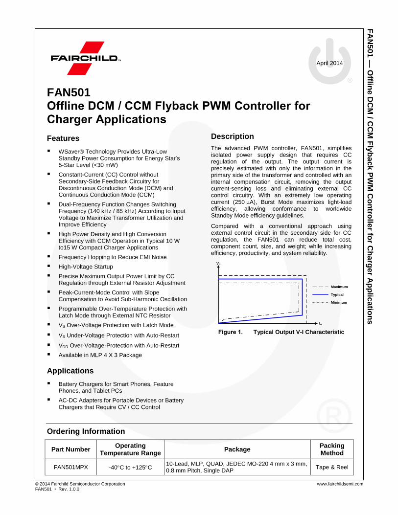
FAN501 Offline DCM / CCM Flyback PWM Controller for Charger Applications
Features
WSaver® Technology Provides Ultra-Low Standby Power Consumption for Energy Star’s 5-Star Level (<30 mW)
Constant-Current (CC) Control without Secondary-Side Feedback Circuitry for Discontinuous Conduction Mode (DCM) and Continuous Conduction Mode (CCM)
Dual-Frequency Function Changes Switching Frequency (140 kHz / 85 kHz) According to Input Voltage to Maximize Transformer Utilization and Improve Efficiency
High Power Density and High Conversion Efficiency with CCM Operation in Typical 10 W to15 W Compact Charger Applications
Frequency Hopping to Reduce EMI Noise
High-Voltage Startup
Precise Maximum Output Power Limit by CC Regulation through External Resistor Adjustment
Peak-Current-Mode Control with Slope Compensation to Avoid Sub-Harmonic Oscillation
Programmable Over-Temperature Protection with Latch Mode through External NTC Resistor
VS Over-Voltage Protection with Latch Mode
VS Under-Voltage Protection with Auto-Restart
VDD Over-Voltage-Protection with Auto-Restart
Available in MLP 4 X 3 Package
Applications
Battery Chargers for Smart Phones, Feature Phones, and Tablet PCs
AC-DC Adapters for Portable Devices or Battery Chargers that Require CV / CC Control
Description
The advanced PWM controller, FAN501, simplifies isolated power supply design that requires CC regulation of the output. The output current is precisely estimated with only the information in the primary side of the transformer and controlled with an internal compensation circuit, removing the output current-sensing loss and eliminating external CC control circuitry. With an extremely low operating current (250 µA), Burst Mode maximizes light-load efficiency, allowing conformance to worldwide Standby Mode efficiency guidelines.
Compared with a conventional approach using external control circuit in the secondary side for CC regulation, the FAN501 can reduce total cost, component count, size, and weight; while increasing efficiency, productivity, and system reliability.
Maximum
Vo
Minimum
Typical
Io Figure 1. Typical Output V-I Characteristic
Ordering Information
Part Number Operating
Temperature Range Package
Packing Method
FAN501MPX -40C to +125C 10-Lead, MLP, QUAD, JEDEC MO-220 4 mm x 3 mm, 0.8 mm Pitch, Single DAP
Tape & Reel
© 2014 Fairchild Semiconductor Corporation www.fairchildsemi.com FAN501 • Rev. 1.0.0 2
FA
N5
01
— O
ffline D
CM
/ CC
M F
lyb
ac
k P
WM
Co
ntro
ller fo
r Ch
arg
er A
pp
lica
tion
s
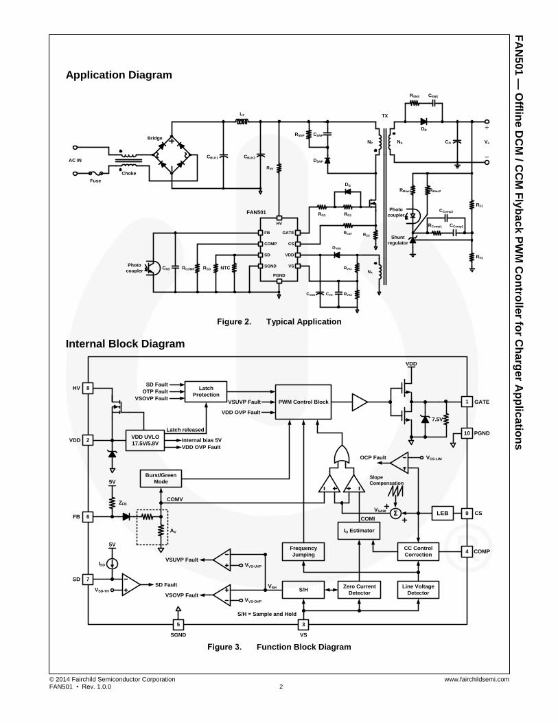
Application Diagram
RSNP CSNP
DSNP
RG1RG2
DG
GATEFB
CS
VDD
VS
COMP
SD
SGND
HV
PGND
RCSRCSF
RVS1
RVS2CVSCVDD
DVDD
CBLK2CBLK1
LF
RHV
NTCRCOMPCFB
Bridge
Choke
Fuse
Photo
coupler
AC IN
FAN501
NP NS
NA
TX
Photo
coupler
RSNS CSNS
DR
CO
RF1
RF2
RBias1 RBias2
Shunt
regulator
CComp2
RComp1 CComp1
Vo
+
-
RSD
Figure 2. Typical Application
Internal Block Diagram
VDD UVLO
17.5V/5.8V
8
LEB
2 Internal bias 5V
VDD OVP Fault
Latch released
1
VDD
3
S/HZero Current
Detector
Line Voltage
Detector
9
4CC Control
Correction
6
ISD
5V
5V
7SD Fault
VSD-TH
ZFB
PWM Control Block
VVS-OVP
Burst/Green
Mode
Σ
Frequency
Jumping
IO Estimator
VCS-LIM
AV
VSOVP Fault
OCP Fault
Latch
Protection
SD Fault
OTP Fault
VSOVP FaultVSUVP Fault
VDD OVP Fault
S/H = Sample and Hold
10
5
GATE
SGND
PGND
CS
COMP
VDD
HV
FB
SD
VS
Slope
Compensation
COMV
COMI
VSH
7.5V
VSAW
VVS-UVP
VSUVP Fault
Figure 3. Function Block Diagram
© 2014 Fairchild Semiconductor Corporation www.fairchildsemi.com FAN501 • Rev. 1.0.0 3
FA
N5
01
— O
ffline D
CM
/ CC
M F
lyb
ac
k P
WM
Co
ntro
ller fo
r Ch
arg
er A
pp
lica
tion
s
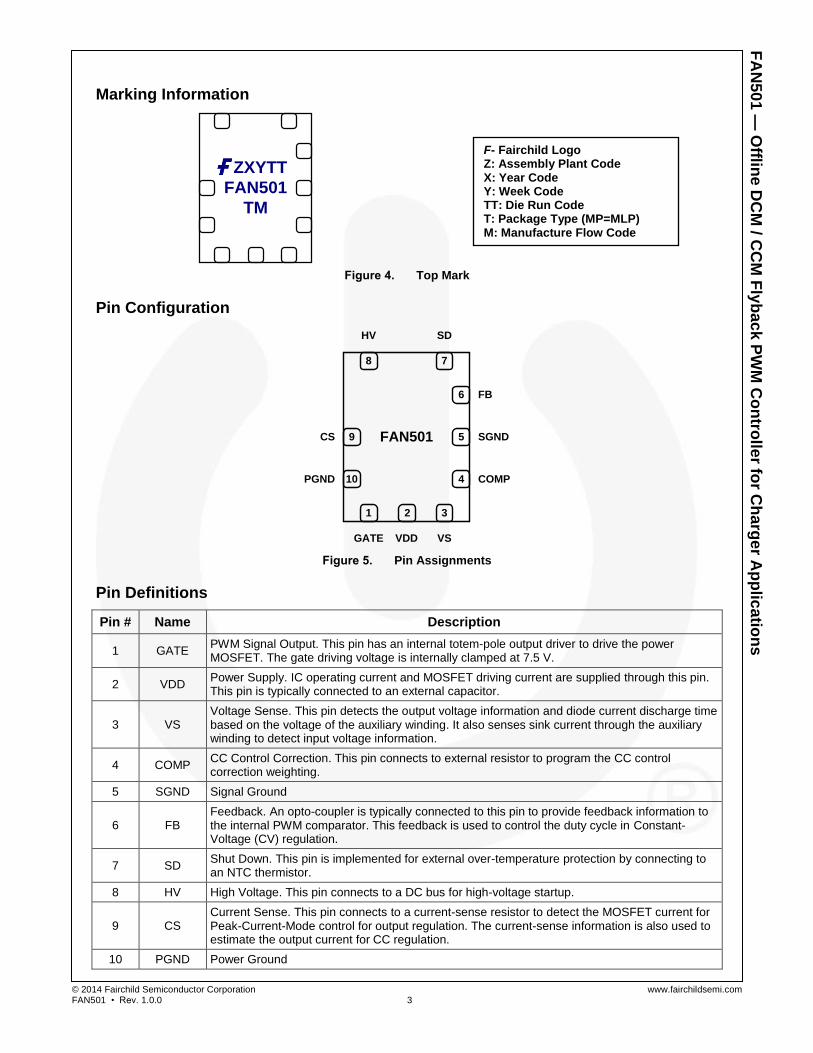
Marking Information
ZXYTT
FAN501
TM
Figure 4. Top Mark
Pin Configuration
GATE
10
9
8 7
5
4
321
6
FAN501
VDD VS
COMP
SGND
FB
HV SD
PGND
CS
Figure 5. Pin Assignments
Pin Definitions
Pin # Name Description
1 GATE PWM Signal Output. This pin has an internal totem-pole output driver to drive the power MOSFET. The gate driving voltage is internally clamped at 7.5 V.
2 VDD Power Supply. IC operating current and MOSFET driving current are supplied through this pin. This pin is typically connected to an external capacitor.
3 VS Voltage Sense. This pin detects the output voltage information and diode current discharge time based on the voltage of the auxiliary winding. It also senses sink current through the auxiliary winding to detect input voltage information.
4 COMP CC Control Correction. This pin connects to external resistor to program the CC control correction weighting.
5 SGND Signal Ground
6 FB Feedback. An opto-coupler is typically connected to this pin to provide feedback information to the internal PWM comparator. This feedback is used to control the duty cycle in Constant-Voltage (CV) regulation.
7 SD Shut Down. This pin is implemented for external over-temperature protection by connecting to an NTC thermistor.
8 HV High Voltage. This pin connects to a DC bus for high-voltage startup.
9 CS Current Sense. This pin connects to a current-sense resistor to detect the MOSFET current for Peak-Current-Mode control for output regulation. The current-sense information is also used to estimate the output current for CC regulation.
10 PGND Power Ground
F- Fairchild Logo Z: Assembly Plant Code X: Year Code Y: Week Code TT: Die Run Code T: Package Type (MP=MLP) M: Manufacture Flow Code
© 2014 Fairchild Semiconductor Corporation www.fairchildsemi.com FAN501 • Rev. 1.0.0 4
FA
N5
01
— O
ffline D
CM
/ CC
M F
lyb
ac
k P
WM
Co
ntro
ller fo
r Ch
arg
er A
pp
lica
tion
s
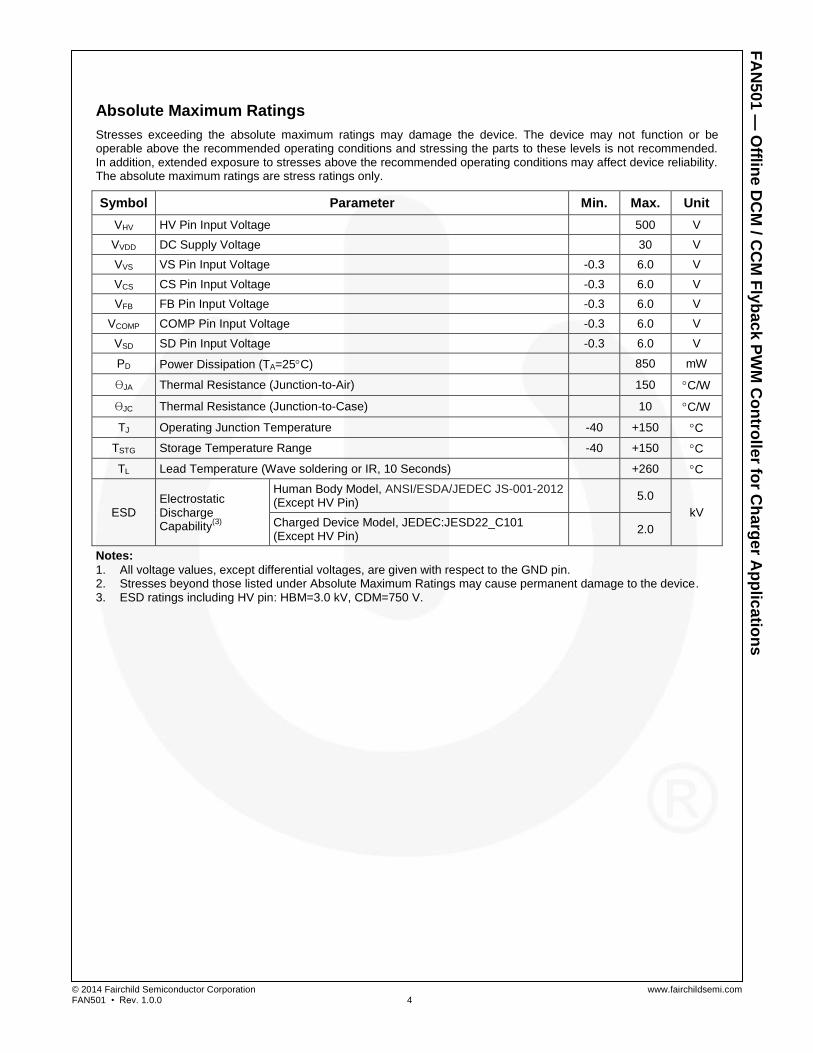
Absolute Maximum Ratings
Stresses exceeding the absolute maximum ratings may damage the device. The device may not function or be operable above the recommended operating conditions and stressing the parts to these levels is not recommended. In addition, extended exposure to stresses above the recommended operating conditions may affect device reliability. The absolute maximum ratings are stress ratings only.
Symbol Parameter Min. Max. Unit
VHV HV Pin Input Voltage 500 V
VVDD DC Supply Voltage 30 V
VVS VS Pin Input Voltage -0.3 6.0 V
VCS CS Pin Input Voltage -0.3 6.0 V
VFB FB Pin Input Voltage -0.3 6.0 V
VCOMP COMP Pin Input Voltage -0.3 6.0 V
VSD SD Pin Input Voltage -0.3 6.0 V
PD Power Dissipation (TA=25C) 850 mW
θJA Thermal Resistance (Junction-to-Air) 150 C/W
θJC Thermal Resistance (Junction-to-Case) 10 C/W
TJ Operating Junction Temperature -40 +150 C
TSTG Storage Temperature Range -40 +150 C
TL Lead Temperature (Wave soldering or IR, 10 Seconds) +260 C
ESD Electrostatic Discharge Capability
(3)
Human Body Model, ANSI/ESDA/JEDEC JS-001-2012 (Except HV Pin)
5.0
kV Charged Device Model, JEDEC:JESD22_C101 (Except HV Pin)
2.0
Notes:
1. All voltage values, except differential voltages, are given with respect to the GND pin. 2. Stresses beyond those listed under Absolute Maximum Ratings may cause permanent damage to the device. 3. ESD ratings including HV pin: HBM=3.0 kV, CDM=750 V.
© 2014 Fairchild Semiconductor Corporation www.fairchildsemi.com FAN501 • Rev. 1.0.0 5
FA
N5
01
— O
ffline D
CM
/ CC
M F
lyb
ac
k P
WM
Co
ntro
ller fo
r Ch
arg
er A
pp
lica
tion
s
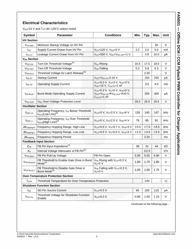
Electrical Characteristics
VDD=15 V and TJ=-40~125C unless noted.
Symbol Parameter Conditions Min. Typ. Max. Unit
HV Section
VHV-MIN Minimum Startup Voltage on HV Pin 30 V
IHV Supply Current Drawn from HV Pin VHV=120 V, VDD=0 V 1.2 2.0 5.0 mA
IHV-LC Leakage Current Drawn from HV Pin VHV=500 V, VDD=VDD-OFF+1 V 0.8 10.0 μA
VDD Section
VDD-ON Turn-On Threshold Voltage(4)
VDD Rising 16.5 17.5 18.5 V
VDD-OFF Turn-Off Threshold Voltage VDD Falling 5.3 5.8 6.3 V
VDD-DLH Threshold Voltage for Latch Release(5)
2.50 V
IDD-ST Startup Current VDD=VDD-ON-0.16 V 150 250 μA
IDD-OP Operating Supply Current VCS=5.0 V, VS=3 V, VFB=3 V, VDD=15 V, CGATE=1 nF
3.5 4.0 mA
IDD-Burst Burst Mode Operating Supply Current VCS=0.3 V, VS=0 V, VFB=0 V, VDD=VDD-ONVDD-OVP10 V, CGATE=1 nF
250 300 μA
VDD-OVP VDD Over-Voltage Protection Level 26.5 28.0 29.5 V
Oscillator Section
fOSC--H Operating Frequency, IVS Below Threshold IVS-L(Low Line)
(4)
VCS=5 V, VS=2.5 V, VFB=6 V 133 140 147 kHz
fOSC--L Operating Frequency, IVS Over Threshold IVS-H(High Line)
(4)
VCS=5 V, VS=2.5 V, VFB=4 V 79 85 91 kHz
ΔfHopping-H Frequency Hopping Range, High Line VCS=0.5 V, VS=0.7 V, VFB=3 V ±5.5 ±7.0 ±8.5 kHz
ΔfHopping-L Frequency Hopping Range, Low Line VCS=0.5 V, VS=0.0 V, VFB=3 V ±2.5 ±4.0 ±5.5 kHz
ΔtHopping Frequency Hopping Period 2.54 ms
Feedback Input Section
ZFB FB Pin Input Impedance(4)
38 41 44 kΩ
AV Internal Voltage Attenuator of FB Pin(5)
1/2.5 V/V
VFB-Open FB Pin Pull-Up Voltage FB Pin Open 5.00 5.50 5.90 V
VFB-Burst-H FB Threshold to Enable Gate Drive in Burst Mode
(4)
VFB Rising with VCS=0.3 V, VS=0 V
1.60 1.70 1.80 V
VFB-Burst-L FB Threshold to Disable Gate Drive in Burst Mode
(4)
VFB Falling with VCS=0.3 V, VS=0 V
1.55 1.65 1.75 V
Over-Temperature Protection Section
TOTP Threshold Temperature for Over-Temperature Protection 140 C
Shutdown Function Section
ISD SD Pin Source Current VCS=0.3 V 85 100 115 μA
VSD-TH Threshold Voltage for Shutdown Function Enable
VCS=0.3 V 0.85 1.00 1.15 V
Continued on the following page…
© 2014 Fairchild Semiconductor Corporation www.fairchildsemi.com FAN501 • Rev. 1.0.0 6
FA
N5
01
— O
ffline D
CM
/ CC
M F
lyb
ac
k P
WM
Co
ntro
ller fo
r Ch
arg
er A
pp
lica
tion
s
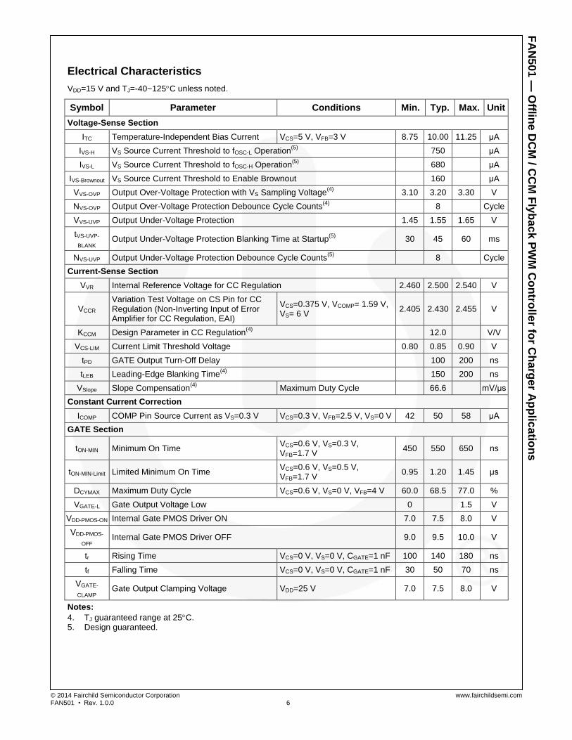
Electrical Characteristics
VDD=15 V and TJ=-40~125C unless noted.
Symbol Parameter Conditions Min. Typ. Max. Unit
Voltage-Sense Section
ITC Temperature-Independent Bias Current VCS=5 V, VFB=3 V 8.75 10.00 11.25 μA
IVS-H VS Source Current Threshold to fOSC-L Operation(5)
750 μA
IVS-L VS Source Current Threshold to fOSC-H Operation(5)
680 μA
IVS-Brownout VS Source Current Threshold to Enable Brownout 160 μA
VVS-OVP Output Over-Voltage Protection with VS Sampling Voltage(4)
3.10 3.20 3.30 V
NVS-OVP Output Over-Voltage Protection Debounce Cycle Counts(4)
8 Cycle
VVS-UVP Output Under-Voltage Protection 1.45 1.55 1.65 V
tVS-UVP-
BLANK Output Under-Voltage Protection Blanking Time at Startup
(5) 30 45 60 ms
NVS-UVP Output Under-Voltage Protection Debounce Cycle Counts(5)
8 Cycle
Current-Sense Section
VVR Internal Reference Voltage for CC Regulation 2.460 2.500 2.540 V
VCCR Variation Test Voltage on CS Pin for CC Regulation (Non-Inverting Input of Error Amplifier for CC Regulation, EAI)
VCS=0.375 V, VCOMP= 1.59 V, VS= 6 V
2.405 2.430 2.455 V
KCCM Design Parameter in CC Regulation(4)
12.0 V/V
VCS-LIM Current Limit Threshold Voltage 0.80 0.85 0.90 V
tPD GATE Output Turn-Off Delay 100 200 ns
tLEB Leading-Edge Blanking Time(4)
150 200 ns
VSlope Slope Compensation(4)
Maximum Duty Cycle 66.6 mV/μs
Constant Current Correction
ICOMP COMP Pin Source Current as VS=0.3 V VCS=0.3 V, VFB=2.5 V, VS=0 V 42 50 58 μA
GATE Section
tON-MIN Minimum On Time VCS=0.6 V, VS=0.3 V, VFB=1.7 V
450 550 650 ns
tON-MIN-Limit Limited Minimum On Time VCS=0.6 V, VS=0.5 V, VFB=1.7 V
0.95 1.20 1.45 μs
DCYMAX Maximum Duty Cycle VCS=0.6 V, VS=0 V, VFB=4 V 60.0 68.5 77.0 %
VGATE-L Gate Output Voltage Low 0 1.5 V
VDD-PMOS-ON Internal Gate PMOS Driver ON 7.0 7.5 8.0 V
VDD-PMOS-
OFF Internal Gate PMOS Driver OFF 9.0 9.5 10.0 V
tr Rising Time VCS=0 V, VS=0 V, CGATE=1 nF 100 140 180 ns
tf Falling Time VCS=0 V, VS=0 V, CGATE=1 nF 30 50 70 ns
VGATE-
CLAMP Gate Output Clamping Voltage VDD=25 V 7.0 7.5 8.0 V
Notes:
4. TJ guaranteed range at 25C. 5. Design guaranteed.
© 2014 Fairchild Semiconductor Corporation www.fairchildsemi.com FAN501 • Rev. 1.0.0 7
FA
N5
01
— O
ffline D
CM
/ CC
M F
lyb
ac
k P
WM
Co
ntro
ller fo
r Ch
arg
er A
pp
lica
tion
s
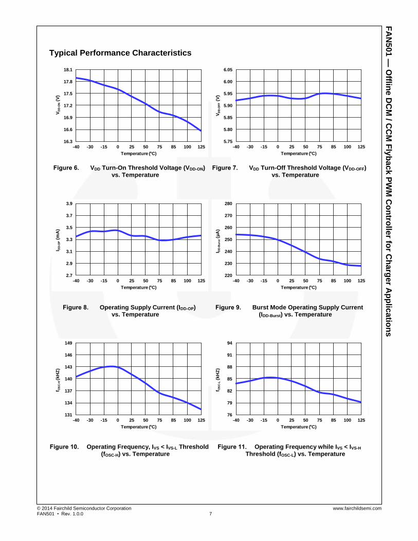
Typical Performance Characteristics
Figure 6. VDD Turn-On Threshold Voltage (VDD-ON) vs. Temperature
Figure 7. VDD Turn-Off Threshold Voltage (VDD-OFF) vs. Temperature
Figure 8. Operating Supply Current (IDD-OP) vs. Temperature
Figure 9. Burst Mode Operating Supply Current (IDD-Burst) vs. Temperature
Figure 10. Operating Frequency, IVS < IVS-L Threshold (fOSC-H) vs. Temperature
Figure 11. Operating Frequency while IVS < IVS-H Threshold (fOSC-L) vs. Temperature
16.3
16.6
16.9
17.2
17.5
17.8
18.1
-40 -30 -15 0 25 50 75 85 100 125
VD
D-O
N(V
)
Temperature ( C)
5.75
5.80
5.85
5.90
5.95
6.00
6.05
-40 -30 -15 0 25 50 75 85 100 125
VD
D-O
FF
(V)
Temperature ( C)
2.7
2.9
3.1
3.3
3.5
3.7
3.9
-40 -30 -15 0 25 50 75 85 100 125
I DD
-OP
(mA
)
Temperature ( C)
220
230
240
250
260
270
280
-40 -30 -15 0 25 50 75 85 100 125
I DD
-Bu
rst(µ
A)
Temperature ( C)
131
134
137
140
143
146
149
-40 -30 -15 0 25 50 75 85 100 125
f OS
C-H
(kH
Z)
Temperature ( C)
76
79
82
85
88
91
94
-40 -30 -15 0 25 50 75 85 100 125
f OS
C-L
(kH
Z)
Temperature ( C)
© 2014 Fairchild Semiconductor Corporation www.fairchildsemi.com FAN501 • Rev. 1.0.0 8
FA
N5
01
— O
ffline D
CM
/ CC
M F
lyb
ac
k P
WM
Co
ntro
ller fo
r Ch
arg
er A
pp
lica
tion
s
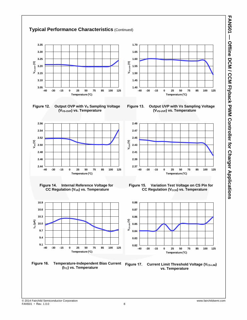
Typical Performance Characteristics (Continued)
Figure 12. Output OVP with VS Sampling Voltage
(VVS-OVP) vs. Temperature
Figure 13. Output UVP with Vs Sampling Voltage (VVS-UVP) vs. Temperature
Figure 14. Internal Reference Voltage for CC Regulation (VVR) vs. Temperature
Figure 15. Variation Test Voltage on CS Pin for CC Regulation (VCCR) vs. Temperature
Figure 16. Temperature-Independent Bias Current (ITC) vs. Temperature
Figure 17. Current Limit Threshold Voltage (VCS-LIM) vs. Temperature
3.05
3.10
3.15
3.20
3.25
3.30
3.35
-40 -30 -15 0 25 50 75 85 100 125
VV
S-O
VP
(V)
Temperature ( C)
1.40
1.45
1.50
1.55
1.60
1.65
1.70
-40 -30 -15 0 25 50 75 85 100 125
VV
S-U
VP
(V)
Temperature ( C)
2.44
2.46
2.48
2.50
2.52
2.54
2.56
-40 -30 -15 0 25 50 75 85 100 125
VV
R(V
)
Temperature ( C)
2.37
2.39
2.41
2.43
2.45
2.47
2.49
-40 -30 -15 0 25 50 75 85 100 125
VC
CR
(V)
Temperature ( C)
9.1
9.4
9.7
10.0
10.3
10.6
10.9
-40 -30 -15 0 25 50 75 85 100 125
I TC
(µA
)
Temperature ( C)
0.82
0.83
0.84
0.85
0.86
0.87
0.88
-40 -30 -15 0 25 50 75 85 100 125
VC
S-L
IM(V
)
Temperature ( C)
© 2014 Fairchild Semiconductor Corporation www.fairchildsemi.com FAN501 • Rev. 1.0.0 9
FA
N5
01
— O
ffline D
CM
/ CC
M F
lyb
ac
k P
WM
Co
ntro
ller fo
r Ch
arg
er A
pp
lica
tion
s
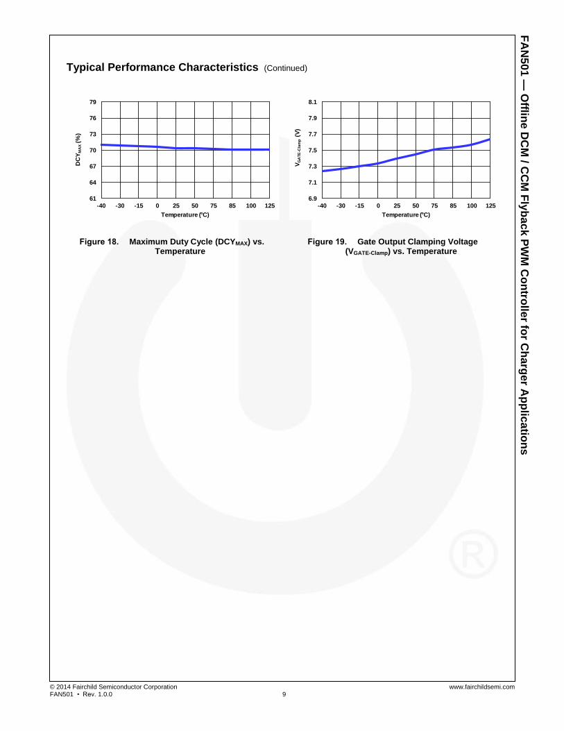
Typical Performance Characteristics (Continued)
Figure 18. Maximum Duty Cycle (DCYMAX) vs. Temperature
Figure 19. Gate Output Clamping Voltage (VGATE-Clamp) vs. Temperature
61
64
67
70
73
76
79
-40 -30 -15 0 25 50 75 85 100 125
DC
YM
AX
(%)
Temperature ( C)
6.9
7.1
7.3
7.5
7.7
7.9
8.1
-40 -30 -15 0 25 50 75 85 100 125
VG
AT
E-C
lam
p(V
)
Temperature ( C)
© 2014 Fairchild Semiconductor Corporation www.fairchildsemi.com FAN501 • Rev. 1.0.0 10
FA
N5
01
— O
ffline D
CM
/ CC
M F
lyb
ac
k P
WM
Co
ntro
ller fo
r Ch
arg
er A
pp
lica
tion
s
Functional Description
FAN501 is an offline flyback converter controller that offers constant output voltage (CV) regulation through opto-coupler feedback circuitry and constant output current (CC) regulation with primary-side control. Advanced output current estimation technology allows stable CC regulation regardless of the power stage operation mode: Continuous Conduction Mode (CCM) or Discontinuous Conduction Mode (DCM).
Dual-switching-frequency operation adaptively selects the operational frequency between 85 kHz and 140 kHz according to the line voltage. As a result, the transformer can be fully utilized and high efficiency is maintained over entire line range. A frequency-hopping function is incorporated to reduce EMI noise.
Line voltage information through transformer auxiliary winding is used for dual-switching frequency selection and CC control correction.
mWSaver® technology, including high-voltage startup and ultra-low operating current in Burst Mode, enables system compliance with Energy Star’s 5-star requirement of <30 mW standby power consumption.
Protections such as VDD Over-Voltage Protection (VDD OVP), VS Over-Voltage Protection (VS OVP), VS Under-Voltage Protection (VS UVP), internal Over-Temperature Protection (OTP), Brownout protection and externally triggered shut-down function improve reliability.
All these innovative technologies allow the FAN501 to offer low total cost, reduced component counts, small size / weight, high conversion efficiency, and high power density for compact charger / adapter applications requiring CV / CC control.
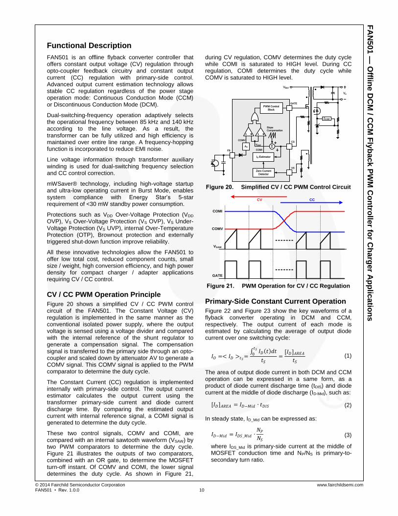
CV / CC PWM Operation Principle
Figure 20 shows a simplified CV / CC PWM control circuit of the FAN501. The Constant Voltage (CV) regulation is implemented in the same manner as the conventional isolated power supply, where the output voltage is sensed using a voltage divider and compared with the internal reference of the shunt regulator to generate a compensation signal. The compensation signal is transferred to the primary side through an opto-coupler and scaled down by attenuator AV to generate a COMV signal. This COMV signal is applied to the PWM comparator to determine the duty cycle.
The Constant Current (CC) regulation is implemented internally with primary-side control. The output current estimator calculates the output current using the transformer primary-side current and diode current discharge time. By comparing the estimated output current with internal reference signal, a COMI signal is generated to determine the duty cycle.
These two control signals, COMV and COMI, are compared with an internal sawtooth waveform (VSAW) by two PWM comparators to determine the duty cycle. Figure 21 illustrates the outputs of two comparators, combined with an OR gate, to determine the MOSFET turn-off instant. Of COMV and COMI, the lower signal determines the duty cycle. As shown in Figure 21,
during CV regulation, COMV determines the duty cycle while COMI is saturated to HIGH level. During CC regulation, COMI determines the duty cycle while COMV is saturated to HIGH level.
Zero Current
Detector
Σ
IO Estimator
PWM Control
Block
AV
Vo
VBLK
Slope
Compenastion
COMV
COMI
VSAW
ZCOMP
GATE
CS
VS
FB
Figure 20. Simplified CV / CC PWM Control Circuit
CV CC
COMV
COMI
VSAW
GATE
Figure 21. PWM Operation for CV / CC Regulation
Primary-Side Constant Current Operation
Figure 22 and Figure 23 show the key waveforms of a flyback converter operating in DCM and CCM, respectively. The output current of each mode is estimated by calculating the average of output diode current over one switching cycle:
𝐼𝑂 =< 𝐼𝐷 >𝑡𝑆= 𝐼𝐷 𝑡 𝑑𝑡𝑡𝑆0
𝑡𝑆=[𝐼𝐷]𝐴𝑅𝐸𝐴
𝑡𝑆 (1)
The area of output diode current in both DCM and CCM operation can be expressed in a same form, as a product of diode current discharge time (tDIS) and diode current at the middle of diode discharge (ID-Mid), such as:
[𝐼𝐷]𝐴𝑅𝐸𝐴 = 𝐼𝐷−𝑀𝑖𝑑 ∙ 𝑡𝐷𝐼𝑆 (2)
In steady state, ID_Mid can be expressed as:
𝐼𝐷−𝑀𝑖𝑑 = 𝐼𝐷𝑆_𝑀𝑖𝑑 ∙𝑁𝑃
𝑁𝑆 (3)
where IDS_Mid is primary-side current at the middle of MOSFET conduction time and NP/NS is primary-to-secondary turn ratio.
© 2014 Fairchild Semiconductor Corporation www.fairchildsemi.com FAN501 • Rev. 1.0.0 11
FA
N5
01
— O
ffline D
CM
/ CC
M F
lyb
ac
k P
WM
Co
ntro
ller fo
r Ch
arg
er A
pp
lica
tion
s
The unified output current equation both for DCM and CCM operation is obtained as:
IO=NPNS
∙IDS_Mid∙tDIStS=NPNS
∙VCS_MidRCS
∙tDIStS
(4)
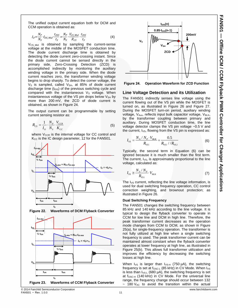
VCS_Mid is obtained by sampling the current-sense voltage at the middle of the MOSFET conduction time. The diode current discharge time is obtained by detecting the diode current zero-crossing instant. Since the diode current cannot be sensed directly in the primary side, Zero-Crossing Detection (ZCD) is accomplished indirectly by monitoring the auxiliary winding voltage in the primary side. When the diode current reaches zero, the transformer winding voltage begins to drop sharply. To detect the corner voltage, the VS is sampled, called VSH, at 85% of diode current discharge time (tDIS) of the previous switching cycle and compared with the instantaneous VS voltage. When instantaneous voltage of the VS pin drops below VSH by more than 200 mV, the ZCD of diode current is obtained, as shown in Figure 24.
The output current can be programmable by setting current sensing resistor as:
1 CCRPCS
O S CC
VNR
I N K (5)
where VCCR is the internal voltage for CC control and KCC is the IC design parameter, 12 for the FAN501.
tON tDIS
tS
IDS
ID
VS
IO = <ID>Ts
ID-Mid = NPS∙IDS-Mid
DCM Waveform
IDS-Mid
½ tON
½ tDIS
Figure 22. Waveforms of DCM Flyback Converter
tON tDIS
tS
IDS
ID
VS
IO = <ID>Ts
ID-Mid = NPS∙IDS-Mid
CCM Waveform
IDS-Mid
½ tON
½ tDIS
Figure 23. Waveforms of CCM Flyback Converter
200mV
0.85∙tDIS(n-1)
tDIS(n)
VS
VSH
ZCD
Figure 24. Operation Waveform for ZCD Function
Line Voltage Detection and its Utilization
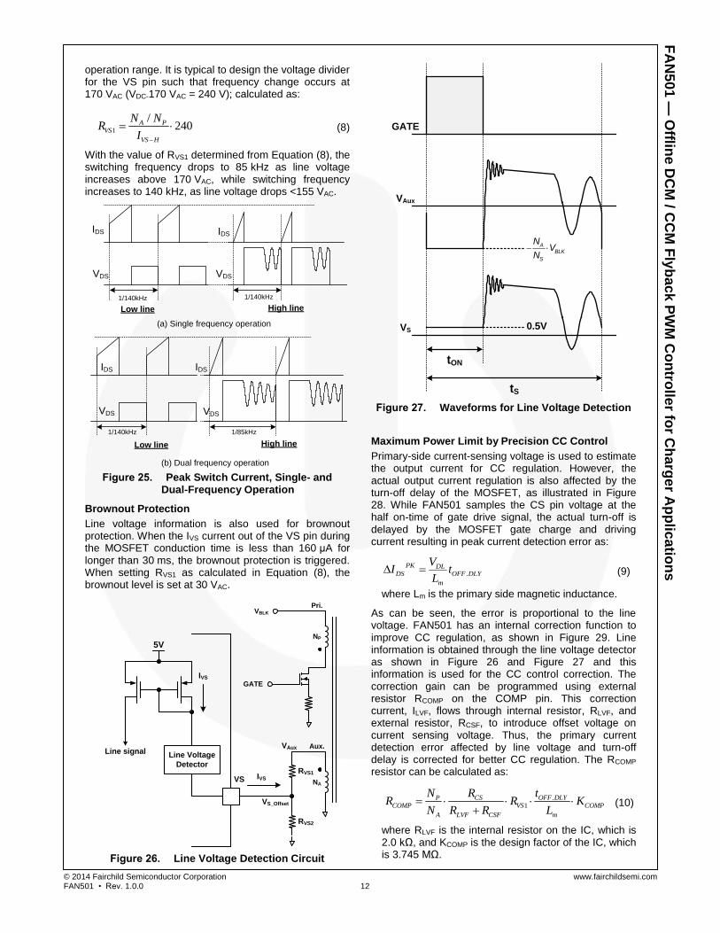
The FAN501 indirectly senses line voltage using the current flowing out of the VS pin while the MOSFET is turned on, as illustrated in Figure 26 and Figure 27. During the MOSFET turn-on period, auxiliary winding voltage, VAux, reflects input bulk capacitor voltage, VBLK, by the transformer coupling between primary and auxiliary. During MOSFET conduction time, the line voltage detector clamps the VS pin voltage ~0.5 V and the current, IVS, flowing from the VS pin is expressed as:
1 1 2
/ 0.5
/ /
A P BLKVS
VS VS VS
N N VI
R R R
+ (6)
Typically, the second term in Equation (6) can be ignored because it is much smaller than the first term. The current, IVS, is approximately proportional to the line voltage, calculated as:
1
/A PVS BLK
VS
N NI V
R
(7)
The IVS current, reflecting the line voltage information, is used for dual switching frequency operation, CC control correction weighting, and brownout protection; as illustrated in Figure 26.
Dual Switching Frequency
The FAN501 changes the switching frequency between 85 kHz and 140 kHz according to the line voltage. It is typical to design the flyback converter to operate in CCM for low line and DCM in high line. Therefore, the peak transformer current decreases as the operation mode changes from CCM to DCM, as shown in Figure 25(a), for single-frequency operation. The transformer is not fully utilized at high line when a single switching frequency is used. The peak transformer current can be maintained almost constant when the flyback converter operates at lower frequency at high line, as illustrated in Figure 25(b). This allows full transformer utilization and improves the efficiency by decreasing the switching losses at high line.
When IVS is larger than IVS-H (750 µA), the switching frequency is set at fOSC-L (85 kHz) in CV Mode. When IVS is less than IVS-L (680 µA), the switching frequency is set at fOSC-H (140 kHz) in CV Mode. For the universal line range, the frequency change should occur between 132 ~ 180 VAC to avoid the transition within the actual
© 2014 Fairchild Semiconductor Corporation www.fairchildsemi.com FAN501 • Rev. 1.0.0 12
FA
N5
01
— O
ffline D
CM
/ CC
M F
lyb
ac
k P
WM
Co
ntro
ller fo
r Ch
arg
er A
pp
lica
tion
s
operation range. It is typical to design the voltage divider for the VS pin such that frequency change occurs at 170 VAC (VDC-170 VAC = 240 V); calculated as:
1
/240A P
VS
VS H
N NR
I -
(8)
With the value of RVS1 determined from Equation (8), the switching frequency drops to 85 kHz as line voltage increases above 170 VAC, while switching frequency increases to 140 kHz, as line voltage drops <155 VAC.
1/140kHz 1/140kHz
Low line High line
IDS IDS
VDS VDS
1/140kHz 1/85kHz
IDS IDS
VDS VDS
Low line High line
(a) Single frequency operation
(b) Dual frequency operation Figure 25. Peak Switch Current, Single- and
Dual-Frequency Operation
Brownout Protection
Line voltage information is also used for brownout protection. When the IVS current out of the VS pin during the MOSFET conduction time is less than 160 μA for longer than 30 ms, the brownout protection is triggered. When setting RVS1 as calculated in Equation (8), the brownout level is set at 30 VAC.
Aux.
VS IVS
Line Voltage
Detector
5V
RVS1
RVS2
IVS
VAux
NA
NP
Pri.VBLK
GATE
Line signal
VS_Offset
Figure 26. Line Voltage Detection Circuit
tON
VAux
VS
GATE
tS
- ABLK
S
NV
N
0.5V
Figure 27. Waveforms for Line Voltage Detection
Maximum Power Limit by Precision CC Control
Primary-side current-sensing voltage is used to estimate the output current for CC regulation. However, the actual output current regulation is also affected by the turn-off delay of the MOSFET, as illustrated in Figure 28. While FAN501 samples the CS pin voltage at the half on-time of gate drive signal, the actual turn-off is delayed by the MOSFET gate charge and driving current resulting in peak current detection error as:
.
PK DLDS OFF DLY
m
VI t
L (9)
where Lm is the primary side magnetic inductance.
As can be seen, the error is proportional to the line voltage. FAN501 has an internal correction function to improve CC regulation, as shown in Figure 29. Line information is obtained through the line voltage detector as shown in Figure 26 and Figure 27 and this information is used for the CC control correction. The correction gain can be programmed using external resistor RCOMP on the COMP pin. This correction current, ILVF, flows through internal resistor, RLVF, and external resistor, RCSF, to introduce offset voltage on current sensing voltage. Thus, the primary current detection error affected by line voltage and turn-off delay is corrected for better CC regulation. The RCOMP resistor can be calculated as:
.
1
CS OFF DLYPCOMP VS COMP
A LVF CSF m
R tNR R K
N R R L
+ (10)
where RLVF is the internal resistor on the IC, which is 2.0 kΩ, and KCOMP is the design factor of the IC, which is 3.745 MΩ.
© 2014 Fairchild Semiconductor Corporation www.fairchildsemi.com FAN501 • Rev. 1.0.0 13
FA
N5
01
— O
ffline D
CM
/ CC
M F
lyb
ac
k P
WM
Co
ntro
ller fo
r Ch
arg
er A
pp
lica
tion
s
The turn-off delay should be obtained by measuring the time between the falling edge and actual turn-off instant of MOSFET, as illustrated in Figure 28.
CS DSR I
.OFF DLYt
DS CSI R
DISt
.DS SH CSI R
.
P
DS SH
S
NI
N
PK
DS CSI R
PK P
D
S
NI
N
(#2)GATE
GSV
Actual diode current
Estimated diode current
Figure 28. CC Control Correction Concept
CC Control
Correction
Line Voltage
DetectorRCSF
CS
COMP
RCS
RCOMPLine Signal
5V
RLVF
ILVF
IO EstimatorZero Current
Detector
VS
RVS1
RVS2
Aux.
Pri.VBLK
GATE
NP
NA
Figure 29. CC Correction Circuit
Pulse-by-Pulse Current Limit
Since the peak transformer current is controlled by a feedback loop, the peak transformer current is not properly controlled when the feedback loop is saturated to HIGH, which typically occurs under startup or overload conditions. To limit the current, a pulse-by-pulse current limit forces the gate drive signal to turn off when the CS pin voltage reaches the current-limit threshold (VCS-LIM) in normal operation.
Burst Mode Operation
The power supply enters Burst Mode at no-load or extremely light-load condition. As shown in Figure 30, when VFB drops below VFB-Burst-L, the PWM output shuts off and the output voltage drops at a rate dependent on load current. This causes the feedback voltage to rise. Once VFB exceeds VFB-Burst-H, the internal circuit starts to provide a switching pulse. The feedback voltage then falls and the process repeats. In this manner, Burst Mode alternately enables and disables switching of the MOSFET to reduce the switching losses in Standby Mode. In Burst Mode, the operating current is reduced from 3.5 mA to 250 μA to minimize power consumption.
VO
VFB
GATE
VFB-Burst-H
VFB-Burst-L
Figure 30. Burst-Mode Operation
Frequency Hopping
EMI reduction is accomplished by frequency hopping, which spreads the energy over a wider frequency range than the bandwidth of the EMI test equipment, allowing compliance with EMI limitations.
Slope Compensation
The sensed voltage across the current-sense resistor is used for current-mode control and pulse-by-pulse current limiting. A synchronized ramp signal with a positive slope is added to the current-sense information at each switching cycle, improving noise immunity during current mode control and avoiding sub-harmonic oscillation during CCM operation.
Leading-Edge Blanking (LEB)
Each time the power MOSFET is switched on, a turn-on spike occurs at the sense resistor. To avoid premature termination of the switching pulse by the spike, a 150 ns leading-edge blanking time is incorporated. Conventional RC filtering can therefore be omitted. During this blanking period, the current-limit comparator is disabled and it cannot switch off the gate driver.
Noise Immunity
Noise from the current sense or the control signal can cause significant pulse-width jitter. Though slope compensation helps alleviate this problem, precautions should be taken to improve the noise immunity. Good placement and layout practices are important. Avoid long PCB traces and component leads and locate bypass capacitor as close to the PWM IC as possible.
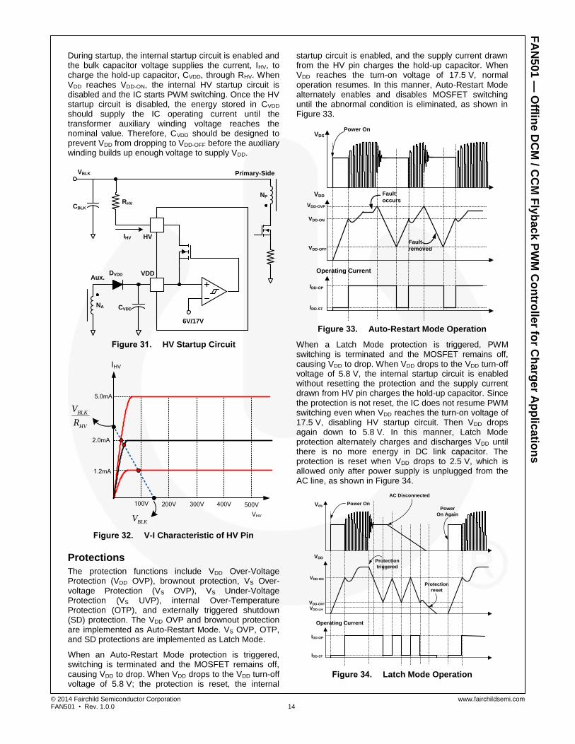
High Voltage (HV) Startup
Figure 31 shows the high-voltage (HV) startup circuit for FAN501 applications. The JFET is used to internally implement the high-voltage current source (see Figure 32 for characteristics). Technically, the HV pin can be directly connected to voltage (VBLK) on an input bulk capacitor. To improve reliability and surge immunity, however, it is typical to use a ~100 kΩ resistor between the HV pin and bulk capacitor voltage. The actual HV current with a given bulk capacitor voltage and startup resistor is determined by the intersection of V-I characteristics line and load line, as shown in Figure 32.
© 2014 Fairchild Semiconductor Corporation www.fairchildsemi.com FAN501 • Rev. 1.0.0 14
FA
N5
01
— O
ffline D
CM
/ CC
M F
lyb
ac
k P
WM
Co
ntro
ller fo
r Ch
arg
er A
pp
lica
tion
s
During startup, the internal startup circuit is enabled and the bulk capacitor voltage supplies the current, IHV, to charge the hold-up capacitor, CVDD, through RHV. When VDD reaches VDD-ON, the internal HV startup circuit is disabled and the IC starts PWM switching. Once the HV startup circuit is disabled, the energy stored in CVDD should supply the IC operating current until the transformer auxiliary winding voltage reaches the nominal value. Therefore, CVDD should be designed to prevent VDD from dropping to VDD-OFF before the auxiliary winding builds up enough voltage to supply VDD.
6V/17V
VDD
RHV
HV
Primary-Side
NP
NA
Aux.
CBLK
VBLK
DVDD
CVDD
IHV
Figure 31. HV Startup Circuit
500V100V 200V 300V 400V
5.0mA
IHV
1.2mA
2.0mA
BLK
HV
V
R
BLKVVHV
Figure 32. V-I Characteristic of HV Pin
Protections
The protection functions include VDD Over-Voltage Protection (VDD OVP), brownout protection, VS Over-voltage Protection (VS OVP), VS Under-Voltage Protection (VS UVP), internal Over-Temperature Protection (OTP), and externally triggered shutdown (SD) protection. The VDD OVP and brownout protection are implemented as Auto-Restart Mode. VS OVP, OTP, and SD protections are implemented as Latch Mode.
When an Auto-Restart Mode protection is triggered, switching is terminated and the MOSFET remains off, causing VDD to drop. When VDD drops to the VDD turn-off voltage of 5.8 V; the protection is reset, the internal
startup circuit is enabled, and the supply current drawn from the HV pin charges the hold-up capacitor. When VDD reaches the turn-on voltage of 17.5 V, normal operation resumes. In this manner, Auto-Restart Mode alternately enables and disables MOSFET switching until the abnormal condition is eliminated, as shown in Figure 33.
VDD-OFF
VDD-ON
VDD
VDS
Power On
Operating Current
IDD-OP
IDD-ST
VDD-OVP
Fault
removed
Fault
occurs
Figure 33. Auto-Restart Mode Operation
When a Latch Mode protection is triggered, PWM switching is terminated and the MOSFET remains off, causing VDD to drop. When VDD drops to the VDD turn-off voltage of 5.8 V, the internal startup circuit is enabled without resetting the protection and the supply current drawn from HV pin charges the hold-up capacitor. Since the protection is not reset, the IC does not resume PWM switching even when VDD reaches the turn-on voltage of 17.5 V, disabling HV startup circuit. Then VDD drops again down to 5.8 V. In this manner, Latch Mode protection alternately charges and discharges VDD until there is no more energy in DC link capacitor. The protection is reset when VDD drops to 2.5 V, which is allowed only after power supply is unplugged from the AC line, as shown in Figure 34.
VDD-OFF
VDD-ON
VDD
Vds Power On
Operating Current
IDD-OP
AC Disconnected
VDD-LH
Power
On Again
IDD-ST
Protection
triggered
Protection
reset
Figure 34. Latch Mode Operation
© 2014 Fairchild Semiconductor Corporation www.fairchildsemi.com FAN501 • Rev. 1.0.0 15
FA
N5
01
— O
ffline D
CM
/ CC
M F
lyb
ac
k P
WM
Co
ntro
ller fo
r Ch
arg
er A
pp
lica
tion
s
VDD Over-Voltage-Protection
VDD over-voltage protection prevents damage from over-voltage exceeding the IC voltage rating. When VDD exceeds 28 V due to an abnormal condition, protection is triggered. This protection is typically caused by an open circuit in the secondary-side feedback network.
Brownout Protection
Brownout protection is implemented through line voltage detection circuit using the auxiliary winding, as shown in Figure 26 and Figure 27. When the current flowing out of the VS pin during the MOSFET conduction time is smaller than 160 μA for longer than 30 ms, the brownout protection is triggered.
Over-Temperature Protection (OTP)
If the junction temperature exceeds 140°C (TOTP), the internal temperature-sensing circuit shuts down PWM output and enters Latch Mode protection.
VS Under-Voltage Protection (VS UVP)
Generally, the fold-back point in CC regulation as output drops is determined by the VDD-OFF level. Thus, the fold-back level mainly depends on the characteristics of the VDD diode and transformer. VS under-voltage protection provides accurate fold-back point control to minimize the effect from the external component tolerance. Figure 35 shows the internal circuit for VS UVP. By sampling the auxiliary winding voltage on the VS pin around the end of diode conduction time, the output voltage is indirectly sensed. When VS sampling voltage is less than VVS-UVP (1.55 V) longer than debounce cycles NVS-UVP, VS UVP is triggered and the FAN501 enters Auto-Restart Mode.
To avoid VS UVP triggering during the startup sequence, a startup blanking time, tVS-UVP-BLANK, (45 ms) in included for system power on. For VS pin voltage divider design, RVS1 is obtained from Equation (11) and RVS2 is determined by VS UVP protection function as:
1
2 1 ( 1)O UVP AVS VS
VS UVP S
V NR R
V N
--
-
- (11)
where VO-UVP is the output under-voltage protection level.
S/HD Q
PWM
Counter
Auto Restart
3
Aux.
NA
RVS1
RVS2
1.55V
VSUVP
Dedounce time
Figure 35. VS UVP Protection Circuit
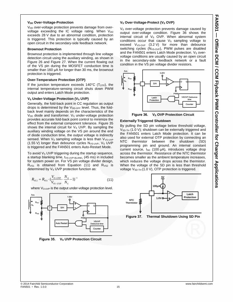
VS Over-Voltage-Protect (VS OVP)
VS over-voltage protection prevents damage caused by output over-voltage condition. Figure 36 shows the internal circuit of VS OVP. When abnormal system conditions occur that cause VS sampling voltage to exceed VVS-OVP (3.2 V) for more than debounce switching cycles (NVS-OVP), PWM pulses are disabled and the FAN501 enters Latch Mode protection. VS over-voltage conditions are usually caused by an open circuit in the secondary-side feedback network or a fault condition in the VS pin voltage divider resistors.
S/HD Q
PWM
Counter
Latch
Protection
Aux.
NA
RVS1
RVS2
3.20V
VSOVP Dedounce
time
Figure 36. VS OVP Protection Circuit
Externally Triggered Shutdown
By pulling the SD pin voltage below threshold voltage, VSD-TH (1.0 V); shutdown can be externally triggered and the FAN501 enters Latch Mode protection. It can be also used for external OTP protection by connecting an NTC thermistor between the shutdown (SD) programming pin and ground. An internal constant current source, ISD (100 µA), introduces voltage drop across the thermistor. Resistance of the NTC thermistor becomes smaller as the ambient temperature increases, which reduces the voltage drops across the thermistor. When the voltage of the SD pin is less than threshold voltage VSD-TH (1.0 V), OTP protection is triggered.
100μA
5V
1.0V
Latch
ProtectionNTC
Thermistor
Figure 37. Thermal Shutdown Using SD Pin
TOP VIEW
AB
4.00
3.00
0.05 C
2X
0.05 C
2X
PIN#1 IDENT
C
0.15±0.05
SEATING
PLANE
0.08 C
0.10 C
0.025±0.025
0.75±0.05
NOTES:
A. DOES NOT FULLY CONFORM TO
JEDEC REGISTRATION, MO-220.
B. DIMENSIONS ARE IN MILLIMETERS.
C. DIMENSIONS AND TOLERANCES PER
ASME Y14.5M, 2009.
D. LAND PATTERN RECOMMENDATION IS
EXISTING INDUSTRY LAND PATTERN.
E. DRAWING FILENAME: MKT-MLP10Hrev2.
1
2
3
4 56
8
7
10 9
FRONT VIEW
SIDE VIEW
SIDE VIEW
BOTTOM VIEW
0.10 C A B
0.05 C
1
2
3
4 56
8
7
10 9
0.80
1.58
1.80
(0.30)
(0.36)
4.60
0.80
1.60
3.60
0.80
0.45
0.40 (10X)
0.65 (10X)
(0.36)
1.58±0.05
0.30(10X)
0.35(10X)
1.80±0.05
0.80
(0.30)
0.80
0.45
CHAMFER 0.25 mm
RECOMMENDED LAND PATTERN
4.00±0.05
3.00±0.05
PIN#1 IDENT
www.onsemi.com1
ON Semiconductor and are trademarks of Semiconductor Components Industries, LLC dba ON Semiconductor or its subsidiaries in the United States and/or other countries.ON Semiconductor owns the rights to a number of patents, trademarks, copyrights, trade secrets, and other intellectual property. A listing of ON Semiconductor’s product/patentcoverage may be accessed at www.onsemi.com/site/pdf/Patent−Marking.pdf. ON Semiconductor reserves the right to make changes without further notice to any products herein.ON Semiconductor makes no warranty, representation or guarantee regarding the suitability of its products for any particular purpose, nor does ON Semiconductor assume any liabilityarising out of the application or use of any product or circuit, and specifically disclaims any and all liability, including without limitation special, consequential or incidental damages.Buyer is responsible for its products and applications using ON Semiconductor products, including compliance with all laws, regulations and safety requirements or standards,regardless of any support or applications information provided by ON Semiconductor. “Typical” parameters which may be provided in ON Semiconductor data sheets and/orspecifications can and do vary in different applications and actual performance may vary over time. All operating parameters, including “Typicals” must be validated for each customerapplication by customer’s technical experts. ON Semiconductor does not convey any license under its patent rights nor the rights of others. ON Semiconductor products are notdesigned, intended, or authorized for use as a critical component in life support systems or any FDA Class 3 medical devices or medical devices with a same or similar classificationin a foreign jurisdiction or any devices intended for implantation in the human body. Should Buyer purchase or use ON Semiconductor products for any such unintended or unauthorizedapplication, Buyer shall indemnify and hold ON Semiconductor and its officers, employees, subsidiaries, affiliates, and distributors harmless against all claims, costs, damages, andexpenses, and reasonable attorney fees arising out of, directly or indirectly, any claim of personal injury or death associated with such unintended or unauthorized use, even if suchclaim alleges that ON Semiconductor was negligent regarding the design or manufacture of the part. ON Semiconductor is an Equal Opportunity/Affirmative Action Employer. Thisliterature is subject to all applicable copyright laws and is not for resale in any manner.
PUBLICATION ORDERING INFORMATIONN. American Technical Support: 800−282−9855 Toll FreeUSA/Canada
Europe, Middle East and Africa Technical Support:Phone: 421 33 790 2910
Japan Customer Focus CenterPhone: 81−3−5817−1050
www.onsemi.com
LITERATURE FULFILLMENT:Literature Distribution Center for ON Semiconductor19521 E. 32nd Pkwy, Aurora, Colorado 80011 USAPhone: 303−675−2175 or 800−344−3860 Toll Free USA/CanadaFax: 303−675−2176 or 800−344−3867 Toll Free USA/CanadaEmail: [email protected]
ON Semiconductor Website: www.onsemi.com
Order Literature: http://www.onsemi.com/orderlit
For additional information, please contact your localSales Representative
© Semiconductor Components Industries, LLC


![Ý Å ï ~X` · iuuqt xxx qsfg gvlvtijnb mh kq tfd g s ðmù d å dy cæ ß ñ a] ñ a¢?: Ê j ø ñ a] » Ñ æ À Ñ z]éØ¿Ä À * è ñ a] éØ¿Ä Ö§ rÚ](https://img.pdfslide.net/doc/110x75/606321c62ab1c9652e2cb3ae/-x-iuuqt-xxx-qsfg-gvlvtijnb-mh-kq-tfd-g-s-m-d-dy-c-a-.jpg)

![¶³Î |Võ Éø¹ò¹Ý ®Ëø·û9£Á³{`Ì]g >4® Õ ] &µW * uõ Î:¿&ójÜ ... · Title ¶³Î |Võ Éø¹ò¹Ý ®Ëø·û9£Á³{`Ì]g_>4® Õ ] &µW * uõ Î:¿&ójÜ Ùup"](https://img.pdfslide.net/doc/110x75/5c75a4ed09d3f2b0618b708d/i-vo-eooy-eou9aig-4-o-w-uo-iojue.jpg)


![éØ¿Ä~*P5~± Ì ·©áæ ó PRè2 èG æ s] é Ø ¿ Ä ~ *P 5 …...éØ¿Ä~*P5~± Ì ·©áæ ó P Rè2 èG æ s] é Ø ¿ Ä ~ *P 5 ·ÛÆ ÔyÌ Ôy t y» C Óé¬åÜ¢](https://img.pdfslide.net/doc/110x75/5e90a73732fcf47bee22c214/p5-oe-pr2-g-s-p-5-p5.jpg)


![Page 1 \ |\ \º-Lº- T * S- A G T] Sº - TEST OF ENGLISH AS A](https://img.pdfslide.net/doc/110x75/5895ad971a28ab86468bc0f1/page-1-o-lo-t-s-a-g-t-so-test-of-english-as-a-.jpg)
![[]lº Ø `qx](https://img.pdfslide.net/doc/110x75/625adaf192f9f974e4766b6e/l-qx.jpg)
![e{ pþ× ÜÖ ´ §»é¬ ]e{Xi^M{ éØ¿ÄËï´ß/cite> · éØ¿ÄËï´ß](https://img.pdfslide.net/doc/110x75/5d1c167b88c993fc268c6c35/e-pb-ueoe-e-exim-eoaeeiaiss-eoaeeiaiss.jpg)