A Readout ASIC for CZT Detectors
Lawrence Jones
ASIC Design GroupScience and Technology Facilities Council
Rutherford Appleton Laboratory
Introduction
PORGAMRAYS is a collaborative project between the Universities of Manchester and Liverpool, and The Science and Technology Facilities Council (STFC)
The Project has been jointly funded by EPSRC and the DTI Technology Programme in the UK
Aim is to develop a demonstrator portable compton gamma camera
Capable of imaging radiation sources and identifying the isotope
It will use Cadmium Zinc Telluride (CZT) room temperature semiconductor
Small size makes it portable and able to operate in hostile environments
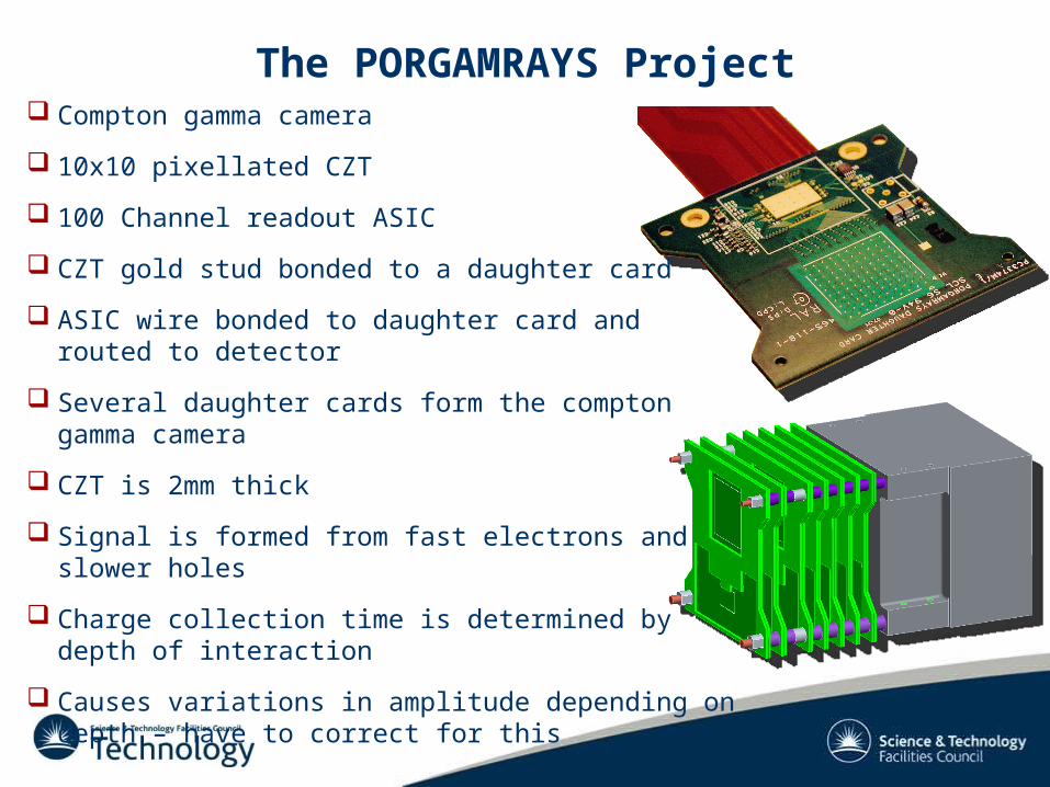
The PORGAMRAYS Project Compton gamma camera
10x10 pixellated CZT
100 Channel readout ASIC
CZT gold stud bonded to a daughter card
ASIC wire bonded to daughter card and routed to detector
Several daughter cards form the compton gamma camera
CZT is 2mm thick
Signal is formed from fast electrons and slower holes
Charge collection time is determined by depth of interaction
Causes variations in amplitude depending on depth – have to correct for this
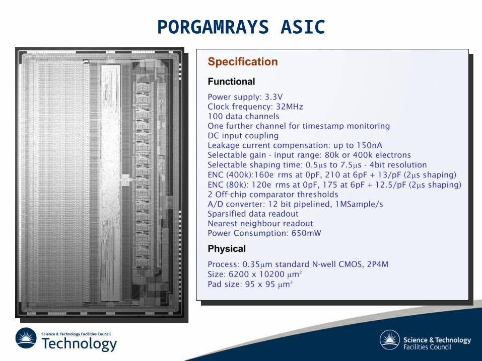
PORGAMRAYS ASIC
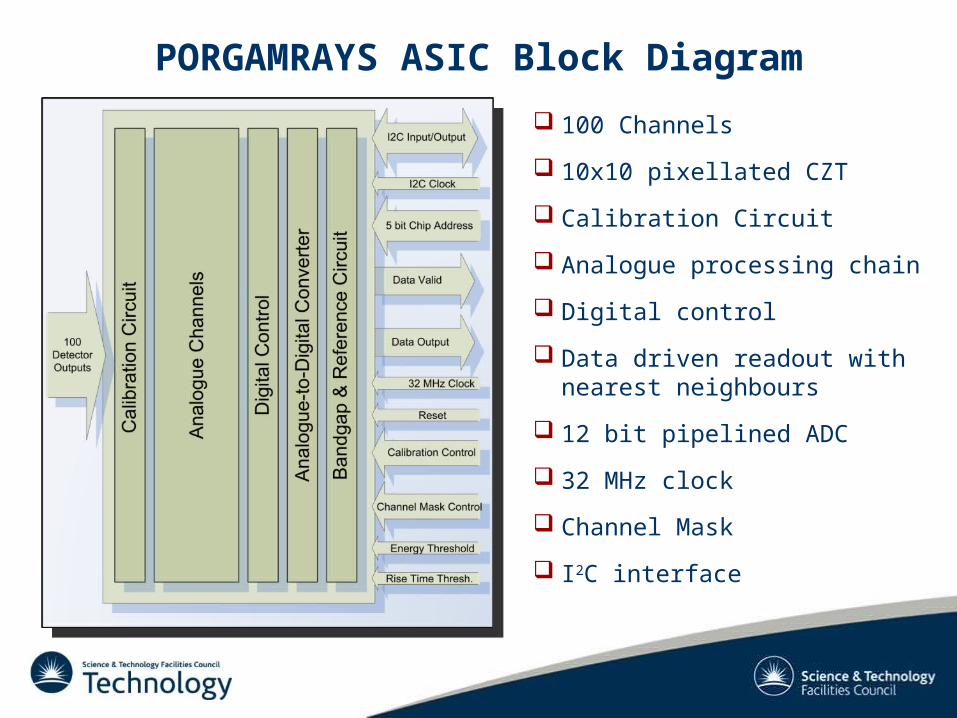
PORGAMRAYS ASIC Block Diagram
100 Channels
10x10 pixellated CZT
Calibration Circuit
Analogue processing chain
Digital control
Data driven readout with nearest neighbours
12 bit pipelined ADC
32 MHz clock
Channel Mask
I2C interface
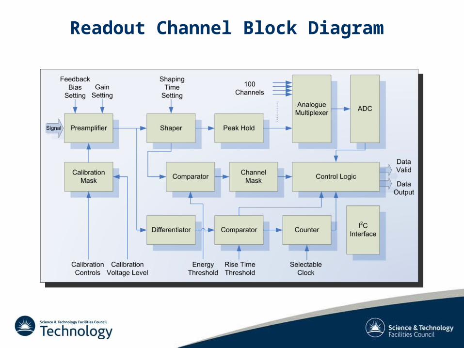
Readout Channel Block Diagram
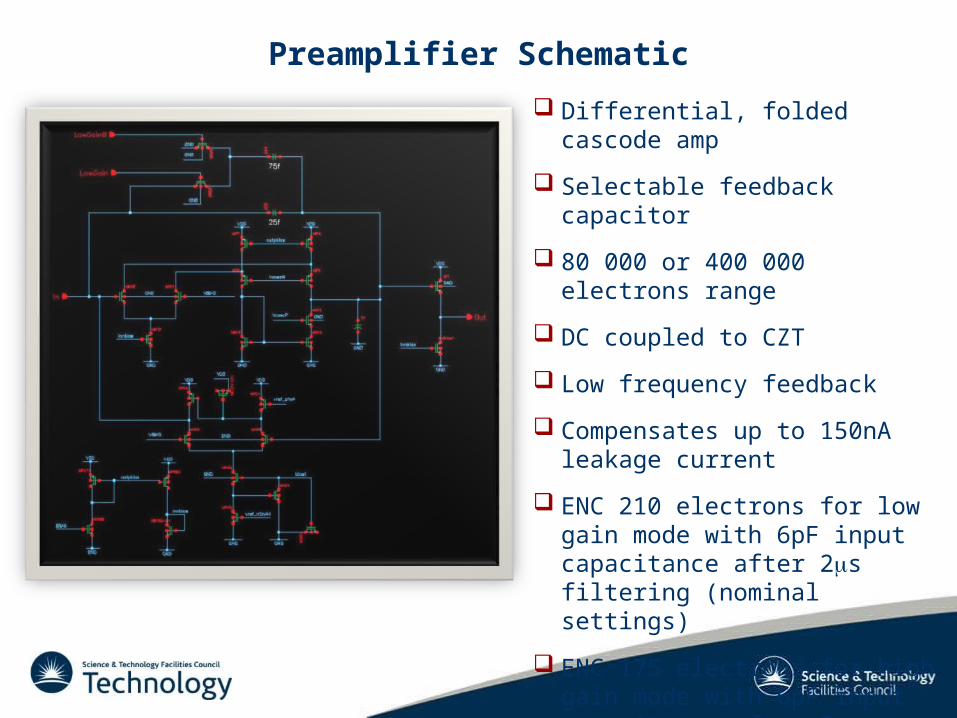
Differential, folded cascode amp
Selectable feedback capacitor
80 000 or 400 000 electrons range
DC coupled to CZT
Low frequency feedback
Compensates up to 150nA leakage current
ENC 210 electrons for low gain mode with 6pF input capacitance after 2s filtering (nominal settings)
ENC 175 electrons for high gain mode with 6pF input capacitance after 2s filtering (nominal settings)
Preamplifier Schematic
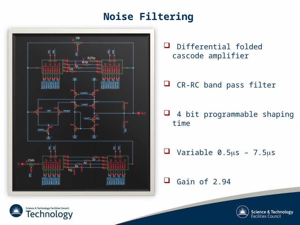
Differential folded cascode amplifier
CR-RC band pass filter
4 bit programmable shaping time
Variable 0.5s – 7.5s
Gain of 2.94
Noise Filtering
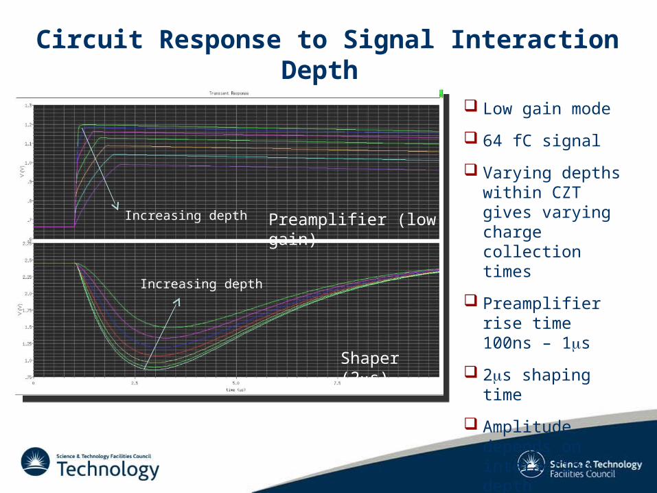
Low gain mode
64 fC signal
Varying depths within CZT gives varying charge collection times
Preamplifier rise time 100ns – 1s
2s shaping time
Amplitude depends on interaction depth
Circuit Response to Signal Interaction Depth
Preamplifier (low gain)
Shaper (2s)
Increasing depth
Increasing depth
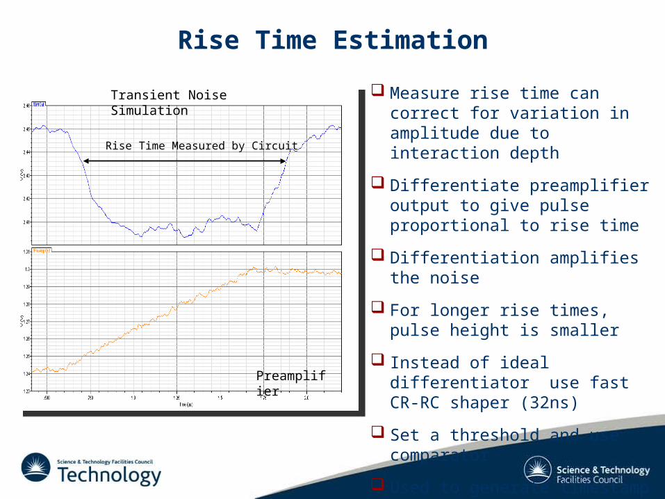
Measure rise time can correct for variation in amplitude due to interaction depth
Differentiate preamplifier output to give pulse proportional to rise time
Differentiation amplifies the noise
For longer rise times, pulse height is smaller
Instead of ideal differentiator use fast CR-RC shaper (32ns)
Set a threshold and use comparator
Used to generate timestamp
Rise Time Estimation
Transient Noise Simulation
Preamplifier
Rise Time Measured by Circuit

Noise Dependence on Preamplifier Feedback Bias
Preamplifier recovery time dependent on preamplifier feedback bias current
Noise increases with increasing bias current
Increasing
Feedback Bias
Current
Noi
se
Input Capacitance
Due to a transistor in the feedback circuit

Charge Sharing and Nearest Neighbour Readout
The charge generated in a CZT detector may be shared between several pixels
If a pixel is above the readout energy threshold then its nearest neighbours are also read out
Mapping between pixel number and channel number is shown on the left
Neighbouring pixels are not necessarily neighbouring channels
Hit ChannelHit Channel + Neighbouring Channels
Lookup TableInput Output
Data Sampling and Conversion
Shaper output is held using a standard Peak Hold circuit
If the data is above threshold (a hit) it will be sampled and converted
The analogue multiplexer runs continuously at the ADC sample rate
The ADC samples those hit channels
All channels not hit are skipped
The ADC is pipelined and converts to 12 bits resolution
All data (Channel No., Rise Time, Time Stamp and ADC) are synchronised
A parallel to serial register shifts the data off chip
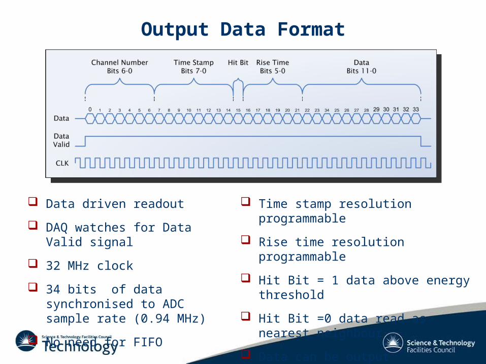
Output Data Format
Data driven readout
DAQ watches for Data Valid signal
32 MHz clock
34 bits of data synchronised to ADC sample rate (0.94 MHz)
No need for FIFO
Time stamp resolution programmable
Rise time resolution programmable
Hit Bit = 1 data above energy threshold
Hit Bit =0 data read as nearest neighbour
Data can be output continuously with no break Data Valid
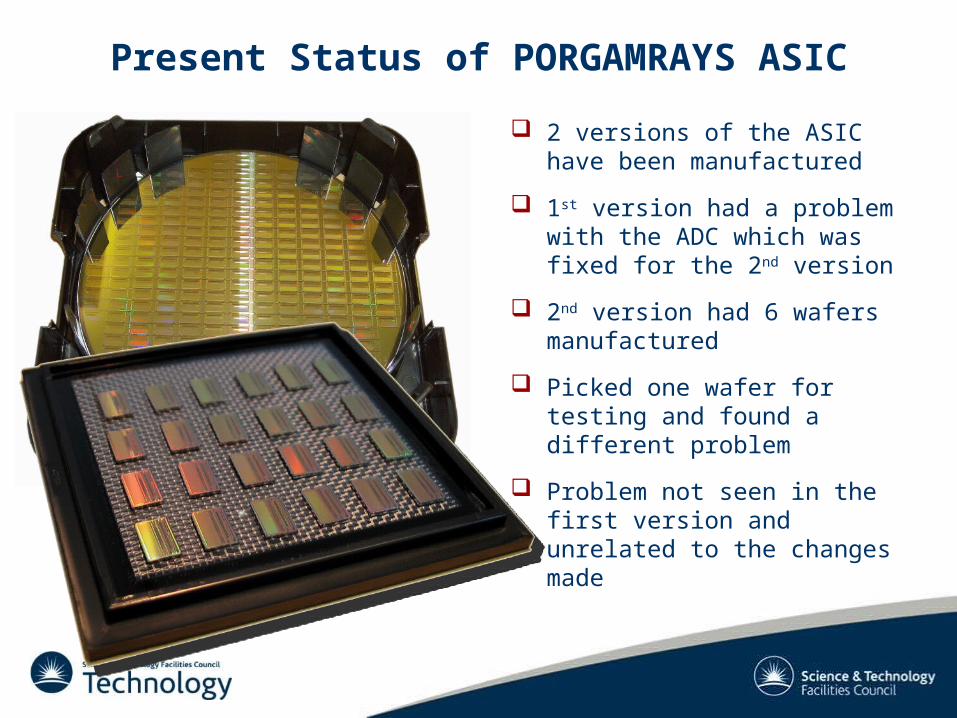
Present Status of PORGAMRAYS ASIC
2 versions of the ASIC have been manufactured
1st version had a problem with the ADC which was fixed for the 2nd version
2nd version had 6 wafers manufactured
Picked one wafer for testing and found a different problem
Problem not seen in the first version and unrelated to the changes made
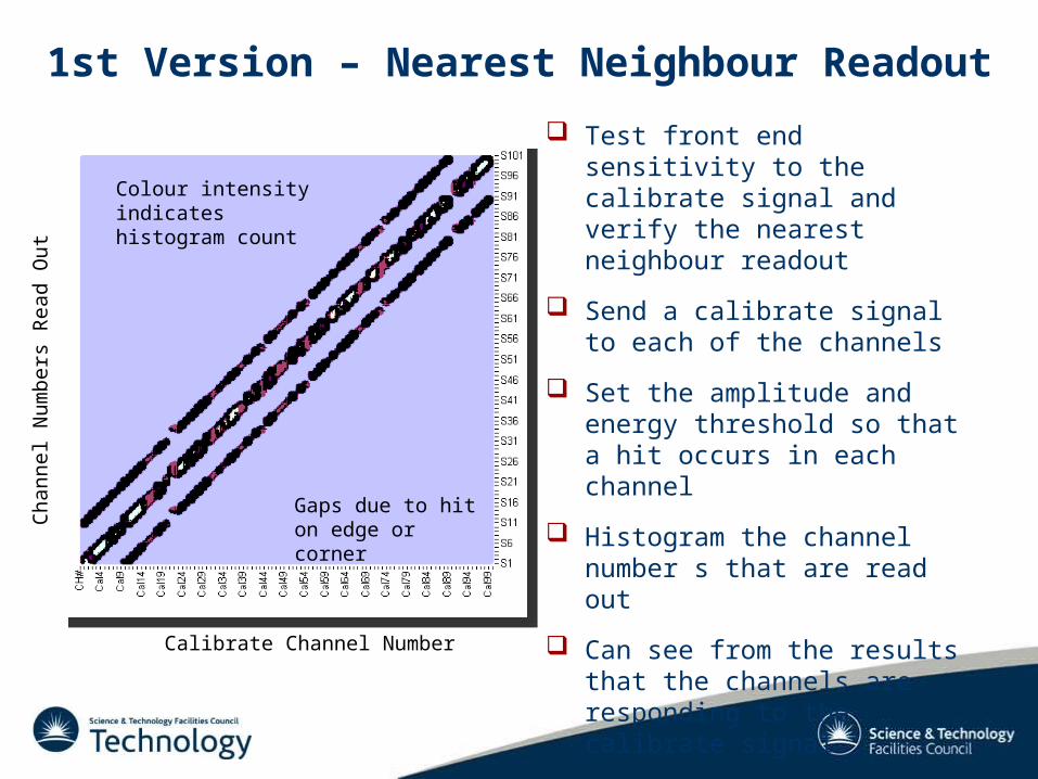
1st Version – Nearest Neighbour Readout
Test front end sensitivity to the calibrate signal and verify the nearest neighbour readout
Send a calibrate signal to each of the channels
Set the amplitude and energy threshold so that a hit occurs in each channel
Histogram the channel number s that are read out
Can see from the results that the channels are responding to the calibrate signal
Nearest neighbour logic is workingCalibrate Channel Number
Cha
nnel
Num
bers
Rea
d O
ut
Gaps due to hit on edge or corner
Colour intensity indicates histogram count
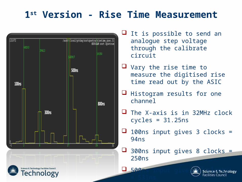
1st Version - Rise Time Measurement
It is possible to send an analogue step voltage through the calibrate circuit
Vary the rise time to measure the digitised rise time read out by the ASIC
Histogram results for one channel
The X-axis is in 32MHz clock cycles = 31.25ns
100ns input gives 3 clocks = 94ns
300ns input gives 8 clocks = 250ns
500ns input gives 17 clocks = 531ns
800ns input gives 26 clocks = 812 ns
Rise time circuit is responsive to input
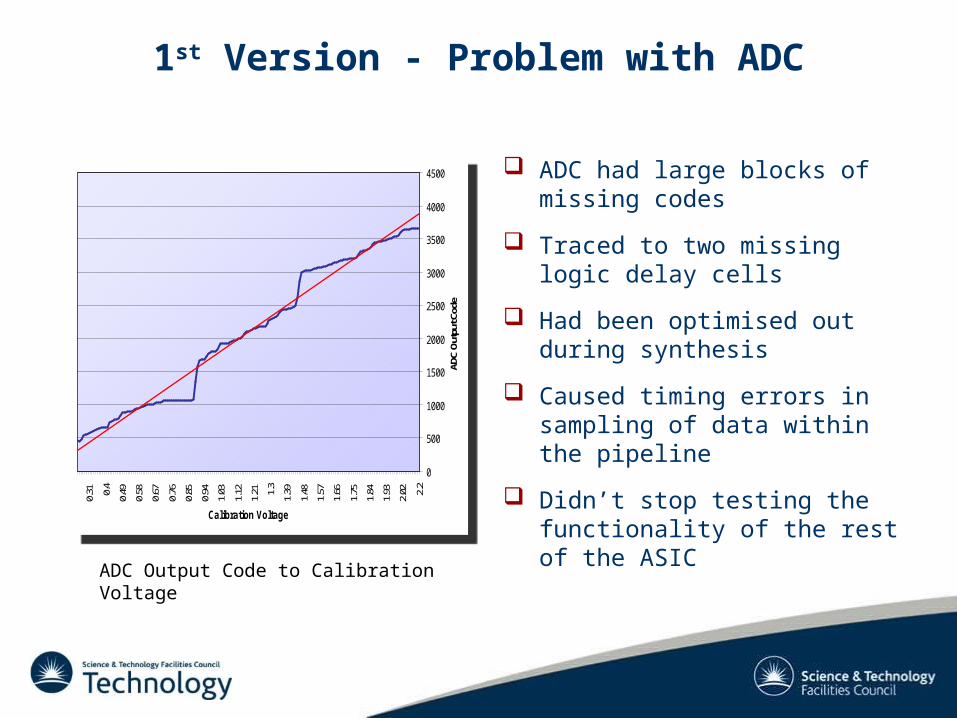
1st Version - Problem with ADC
ADC had large blocks of missing codes
Traced to two missing logic delay cells
Had been optimised out during synthesis
Caused timing errors in sampling of data within the pipeline
Didn’t stop testing the functionality of the rest of the ASIC
0
500
1000
1500
2000
2500
3000
3500
4000
4500
2.2
2.02
1.93
1.84
1.75
1.66
1.57
1.48
1.391.
3
1.21
1.12
1.03
0.94
0.85
0.76
0.67
0.58
0.490.
4
0.31
Calibration Voltage
ADC
Out
put C
ode
0
500
1000
1500
2000
2500
3000
3500
4000
4500
2.2
2.02
1.93
1.84
1.75
1.66
1.57
1.48
1.391.
3
1.21
1.12
1.03
0.94
0.85
0.76
0.67
0.58
0.490.
4
0.31
Calibration Voltage
ADC
Out
put C
ode
ADC Output Code to Calibration Voltage
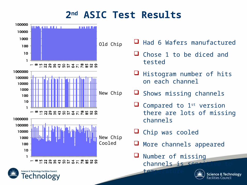
2nd ASIC Test Results
Had 6 Wafers manufactured
Chose 1 to be diced and tested
Histogram number of hits on each channel
Shows missing channels
Compared to 1st version there are lots of missing channels
Chip was cooled
More channels appeared
Number of missing channels is sensitive to temperature
Old Chip
New Chip
New ChipCooled
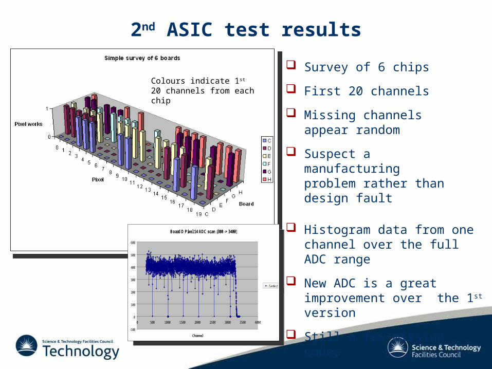
2nd ASIC test results
Survey of 6 chips
First 20 channels
Missing channels appear random
Suspect a manufacturing problem rather than design fault
Board D Pixel 14 ADC scan (300 -> 3400)
-100
0
100
200
300
400
500
600
0 500 1000 1500 2000 2500 3000 3500 4000
Channel
Series1
Board D Pixel 14 ADC scan (300 -> 3400)
-100
0
100
200
300
400
500
600
0 500 1000 1500 2000 2500 3000 3500 4000
Channel
Series1
Histogram data from one channel over the full ADC range
New ADC is a great improvement over the 1st version
Still a few missing codes
Colours indicate 1st 20 channels from each chip
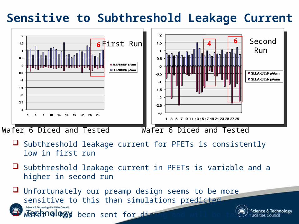
First Run Second Run
Wafer 6 Diced and Tested Wafer 6 Diced and Tested
664
Sensitive to Subthreshold Leakage Current
Subthreshold leakage current for PFETs is consistently low in first run
Subthreshold leakage current in PFETs is variable and a higher in second run
Unfortunately our preamp design seems to be more sensitive to this than simulations predicted
Wafer 4 has been sent for dicing and will be tested
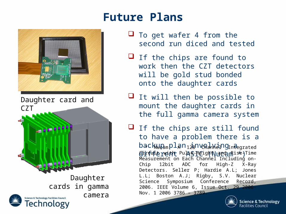
To get wafer 4 from the second run diced and tested
If the chips are found to work then the CZT detectors will be gold stud bonded onto the daughter cards
It will then be possible to mount the daughter cards in the full gamma camera system
If the chips are still found to have a problem there is a backup plan involving a different ASIC (Nucam *)
* Nucam: A 128 Channel Integrated Circuit with Pulse-Height and Rise-Time Measurement on Each Channel Including on-Chip 12bit ADC for High-Z X-Ray Detectors. Seller P; Hardie A.L; Jones L.L; Boston A.J; Rigby, S.V. Nuclear Science Symposium Conference Record, 2006. IEEE Volume 6, Issue Oct. 29 2006-Nov. 1 2006 3786 – 3789.
Future Plans
Daughter card and CZT
Daughter cards in gamma camera
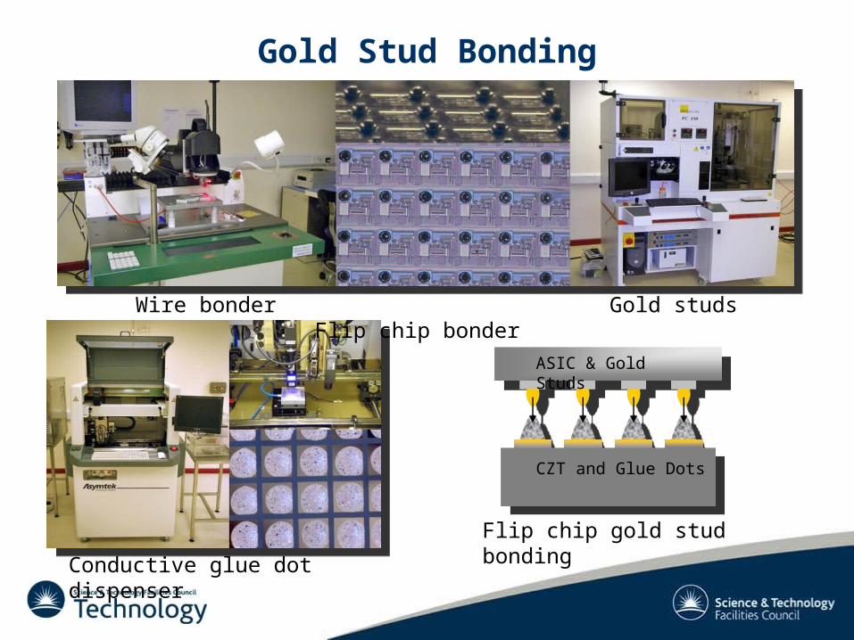
Gold Stud Bonding
Conductive glue dot dispenser
Wire bonder Gold studs Flip chip bonder
Flip chip gold stud bonding
ASIC & Gold Studs
CZT and Glue Dots

Thanks to Ian Lazarus, Paul Seller, Patrick Coleman-Smith
Contact Details
Lawrence JonesIC Design Engineer, ASIC Design Group
Science and Technology Facilities CouncilRutherford Appleton Laboratory, Harwell Science and Innovation Campus,Didcot, OX11 0QX United Kingdom
Tel +44(0)1235 446508 Fax +44(0)1235 445008Email: [email protected]
Thanks for Listening
Recommended


![Latest developments on the highly granular Silicon ... · SKIROC[14] (Silicon pin Kalorimeter Integrated ReadOut Chip) is the very front end ASIC designed for the readout of the Silicon](https://img.pdfslide.net/doc/110x75/5e314b7924ee241cf702c6fd/latest-developments-on-the-highly-granular-silicon-skiroc14-silicon-pin-kalorimeter.jpg)