30 IEEE TRANSACTIONS ON POWER ELECTRONICS, VOL. 18, NO. 1, JANUARY 2003
Analysis of the Snubberless Operation of theEmitter Turn-Off Thyristor (ETO)
Yuxin Li , Member, IEEE, Alex Q. Huang, Senior Member, IEEE, and Kevin Motto
Abstract—The emitter turn-off thyristor (ETO) is a hybridpower semiconductor device that turns off the GTO under theunity turn-off gain condition. This paper analyzes the failuremechanism in the snubberless turn-off of the ETO and proposessolutions that extend the snubberless switching capability ofthe ETO to the theoretical limitation of the device. Theoreticalanalysis and experimental results are presented.
Index Terms—Emitter turn-off, ETO, GTO, IGCT, MTO,thyristor, unity gain turn-off.
I. INTRODUCTION
T HE EMITTER turn-off thyristor (ETO) [1], [10] is a newhybrid power semiconductor device that turns off the gate
turn-off thyristor (GTO) under the unity turn-off gain condition.Theoretical and experimental results have demonstrated the su-perior performance of the ETO over that of traditional GTO’s interms of switching speed, ease of control and maximum control-lable current capability. Compared to the competing technolo-gies such as the Integrated Gate Commutated Thyristor (IGCT)[2], [8], [9], the ETO thyristor provides clear advantages interms of gate drive power requirement and over-current protec-tion capability.
Snubberless switching capability is a very important featureof advanced power semiconductor switches. Traditional GTO’sdo not have this capability because they are turned off with aturn-off gain (defined as ) of higher than one. They de-mand a bulky snubber to shape the voltage waveform,lowering the instant power level during the turn-off transient.The failure mechanism for the traditional GTO turn-off with
snubber has been recognized as current filamentation [3],[13] or nonuniform current re-distribution during the turn-offtransient. There are two distinct processes that can cause thecurrent filamentation in the GTO turn-off. One happens in theturn-off storage-time stage. Due to the nature of nonuniformstorage time among thousands of GTO cells, those cells withlonger storage times will accumulate more current from those
Manuscript received May 26, 2000; revised July 27, 2002. This work wassupported by Sandia National Lab, Westcode Semiconductor Ltd., the Office ofNaval Research, and ERC Shared Facilities supported by the National ScienceFoundation under Award EEC-9731677. This paper was presented at the IEEEInternational Conference on Power Electronics and Drive Systems (PEDS’99),Hong Kong, July 27–29, 1999. Recommended by Associate Editor P. R. Palmer.
Y. Li is with Analog Devices, Inc., San Jose, CA 95134 USA (e-mail:[email protected]).
A. Q. Huang is with the Bradley Department of Electrical and Computer En-gineering, Virginia Polytechnic Institute and State University, Blacksburg, VA24061 USA (e-mail: [email protected]).
K. Motto is with Northrop Grumman Corporation, Sykesville, MD 21784USA (e-mail: [email protected]).
Digital Object Identifier 10.1109/TPEL.2002.807087
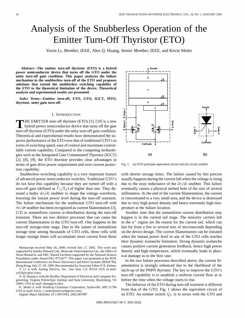
Fig. 1. (a) ETO principle equivalent circuit and (b) circuit symbol.
with shorter storage times. The failure caused by this processusually happens during the current fall when the voltage is risingdue to the stray inductance of the snubber. This failureeventually causes a physical melted hole of the size of severalmillimeters. At the end of the current filamentation, the currentis concentrated to a very small area, and the device is destroyeddue to very high power density and hence extremely high tem-perature at the failure location.
Another time that the nonuniform current distribution mayhappen is in the current tail stage. The minority carriers leftin the n region are the reason for the current tail, which canlast for from a few to several tens of microseconds dependingon the device design. The current filamentation can be initiatedwhen the instant power level in any of the GTO cells reachestheir dynamic avalanche limitation. Strong dynamic avalanchecauses positive current generation feedback, hence high powerdensity and high temperature, which eventually leads to phys-ical damage as in the first case.
In the two failure processes described above, the current fil-amentation is strongly enhanced due to the likelihood of thelatch-up of the PNPN thyristor. The key to improve the GTO’sturn-off capability is to establish a uniform current flow at orbefore the time when the voltage starts to rise.
The behavior of the ETO during turn-off transient is differentfrom that of the GTO. Fig. 1 shows the equivalent circuit ofan ETO. An emitter switch is in series with the GTO and
0885-8993/03$17.00 © 2003 IEEE
LI et al.: SNUBBERLESS OPERATION 31
another switch is connected to the gate of the GTO. Byturning off the and turning on the , the GTO cathodecurrent is completely commutated to its gate and gate switch
. At the end of the turn-off storage stage, the GTO cathodecurrent has already become zero and the GTO is acting as anopen base PNP transistor. The turn-off gain of the GTO in thiscase is unity because its gate and anode current are equal to eachother [12].
Due to the unity-gain turn-off capability, a uniform currentflow has been established (PNP current flow) in the ETO be-fore the voltage starts to rise. Theoretical studies [4], [11] haveproven that the GTO operating under unity turn-off gain has avery good Reverse-Biased-Safe-Operation-Area (RBSOA) andcan even conduct turn-off switching without any snubber.
The ETO improves the RBSOA in two ways. First, the cur-rent filamentation at the storage time phase is basically elim-inated because each GTO cell now has a very similar storagetime due to the unity turn-off gain. Second, the likelihood ofPNPN thyristor latchup in the ETO is greatly reduced duringturn-off because the emitter switch is open. This greatly re-duces the chance of current filamentation caused by dynamicavalanche. Therefore, theoretically, the ETO can have a snub-berless switching capability determined only by the dynamicavalanche breakdown of an open-base PNP transistor.
However, preliminary ETO snubberless turn-off tests failedat various low power levels. This paper analyzes the new failuremechanism in the ETO snubberless operation. Possible solu-tions are also proposed that have expanded the ETO’s snubber-less turn-off capability to more than 200 kW/cm.
II. THEORETICAL DYNAMIC AVALANCHE LIMITATION AND
SNUBBERLESSTURN-OFF FAILURE OF THE ETO
Under the condition of unity turn-off gain, the PNPNlatch mechanism is essentially eliminated and the dynamicperformance of a GTO during turn-off is like an open-basePNP bipolar transistor. If uniform current conduction can bemaintained, the theoretical dynamic avalanche limitation of aPNP transistor is determined by the instant power as [5]
current density;anode to cathode voltage;silicon permittivity, 11.9 8.85 10 F/cm;carrier saturation velocity, 10cm/s;maximum electric field that causes strong avalanchegeneration in lightly doped silicon, typically 210V/cm.
Generally, is in the range of 200300 kW/cm , dependingon the detailed device structure.
ETO1040S, a 1.0 kA, 4.0 kV ETO, has an effective die di-ameter of 4.2 cm, and a silicon area of 14 cm. Assuming auniform current distribution during the entire turn-off transient,it should withstand 2.8 megawatts of instant peak power, or ata DC link voltage of 2.8 kV, this device should withstand snub-berless turn-off at 1 kA current.
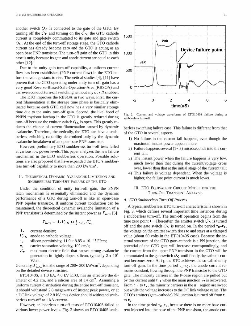
However, snubberless turn-off tests of ETO1040S failed atvarious lower power levels. Fig. 2 shows an ETO1040S snub-
Fig. 2. Current and voltage waveforms of ETO1040S failure during asnubberless turn-off.
berless switching failure case. This failure is different from thatof the GTO in several aspects.
1) No failure in the current fall happens, even though themaximum instant power appears there.
2) Failure happens several (13) microseconds into the cur-rent tail.
3) The instant power when the failure happens is very low,much lower than that during the current/voltage crossover, lower than that at the initial stage of the current tail;
4) This failure is voltage dependent. When the voltage ishigher, the failure point current is much lower.
III. ETO EQUIVALENT CIRCUIT MODEL FOR THE
TURN-OFF TRANSIENT ANALYSIS
A. ETO Snubberless Turn-Off Process
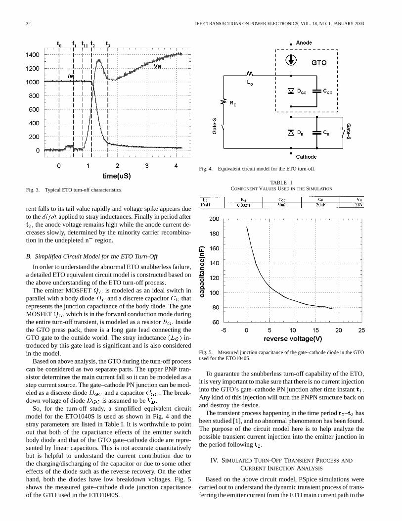
A typical snubberless ETO turn-off characteristic is shown inFig. 3, which defines several important time instances duringa snubberless turn-off. The turn-off operation begins from thetime zero point . Thereafter, the emitter switch is turnedoff and the gate switch is turned on. In the period – ,the voltage on the emitter switch rises to and stays at a clampedvalue (about 60 volts in the ETO1040S case). Because the in-ternal structure of the GTO gate–cathode is a PN junction, thepotential of the GTO gate will increase correspondingly, andthe current from the upper PNP transistor in the GTO will becommutated to the gate switch until finally the cathode cur-rent becomes zero. At , the ETO achieves the so-called unityturn-off gain. In the time period – , the anode current re-mains constant, flowing through the PNP transistor to the GTOgate. The minority carriers in the P-base region are pulled outby this current until when the main junction is recovered.From to , the minority carriers in the nregion are sweptout while the voltage increases to the DC link voltage value. TheGTO’s emitter (gate–cathode) PN junction is turned off fromto .
In the time period – , because there is no more base cur-rent injected into the base of the PNP transistor, the anode cur-
32 IEEE TRANSACTIONS ON POWER ELECTRONICS, VOL. 18, NO. 1, JANUARY 2003
Fig. 3. Typical ETO turn-off characteristics.
rent falls to its tail value rapidly and voltage spike appears dueto the applied to stray inductances. Finally in period after
, the anode voltage remains high while the anode current de-creases slowly, determined by the minority carrier recombina-tion in the undepleted nregion.
B. Simplified Circuit Model for the ETO Turn-Off
In order to understand the abnormal ETO snubberless failure,a detailed ETO equivalent circuit model is constructed based onthe above understanding of the ETO turn-off process.
The emitter MOSFET is modeled as an ideal switch inparallel with a body diode and a discrete capacitor thatrepresents the junction capacitance of the body diode. The gateMOSFET , which is in the forward conduction mode duringthe entire turn-off transient, is modeled as a resistor. Insidethe GTO press pack, there is a long gate lead connecting theGTO gate to the outside world. The stray inductance in-troduced by this gate lead is significant and is also consideredin the model.
Based on above analysis, the GTO during the turn-off processcan be considered as two separate parts. The upper PNP tran-sistor determines the main current fall so it can be modeled as astep current source. The gate–cathode PN junction can be mod-eled as a discrete diode and a capacitor . The break-down voltage of diode is assumed to be .
So, for the turn-off study, a simplified equivalent circuitmodel for the ETO1040S is used as shown in Fig. 4 and thestray parameters are listed in Table I. It is worthwhile to pointout that both of the capacitance effects of the emitter switchbody diode and that of the GTO gate–cathode diode are repre-sented by linear capacitors. This is not accurate quantitativelybut is helpful to understand the current contribution due tothe charging/discharging of the capacitor or due to some othereffects of the diode such as the reverse recovery. On the otherhand, both the diodes have low breakdown voltages. Fig. 5shows the measured gate–cathode diode junction capacitanceof the GTO used in the ETO1040S.
Fig. 4. Equivalent circuit model for the ETO turn-off.
TABLE ICOMPONENTVALUES USED IN THE SIMULATION
Fig. 5. Measured junction capacitance of the gate–cathode diode in the GTOused for the ETO1040S.
To guarantee the snubberless turn-off capability of the ETO,it is very important to make sure that there is no current injectioninto the GTO’s gate–cathode PN junction after time instant.Any kind of this injection will turn the PNPN structure back onand destroy the device.
The transient process happening in the time period– hasbeen studied [1], and no abnormal phenomenon has been found.The purpose of the circuit model here is to help analyze thepossible transient current injection into the emitter junction inthe period following .
IV. SIMULATED TURN-OFF TRANSIENT PROCESS AND
CURRENT INJECTIONANALYSIS
Based on the above circuit model, PSpice simulations werecarried out to understand the dynamic transient process of trans-ferring the emitter current from the ETO main current path to the
LI et al.: SNUBBERLESS OPERATION 33
(a)
(b)
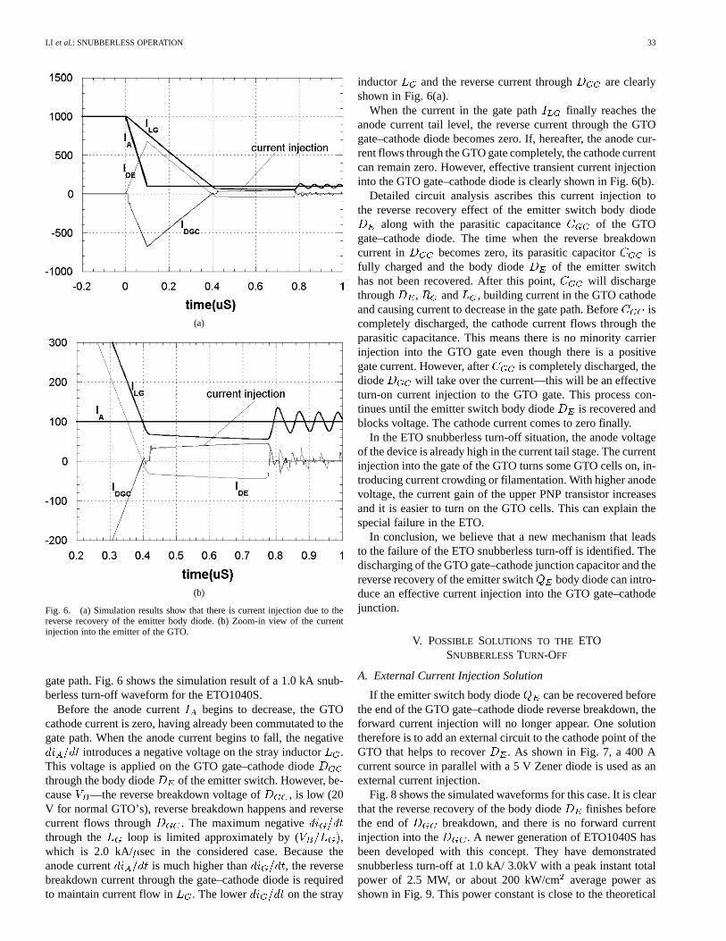
Fig. 6. (a) Simulation results show that there is current injection due to thereverse recovery of the emitter body diode. (b) Zoom-in view of the currentinjection into the emitter of the GTO.
gate path. Fig. 6 shows the simulation result of a 1.0 kA snub-berless turn-off waveform for the ETO1040S.
Before the anode current begins to decrease, the GTOcathode current is zero, having already been commutated to thegate path. When the anode current begins to fall, the negative
introduces a negative voltage on the stray inductor.This voltage is applied on the GTO gate–cathode diodethrough the body diode of the emitter switch. However, be-cause —the reverse breakdown voltage of , is low (20V for normal GTO’s), reverse breakdown happens and reversecurrent flows through . The maximum negativethrough the loop is limited approximately by ( ,which is 2.0 kA/ sec in the considered case. Because theanode current is much higher than , the reversebreakdown current through the gate–cathode diode is requiredto maintain current flow in . The lower on the stray
inductor and the reverse current through are clearlyshown in Fig. 6(a).
When the current in the gate path finally reaches theanode current tail level, the reverse current through the GTOgate–cathode diode becomes zero. If, hereafter, the anode cur-rent flows through the GTO gate completely, the cathode currentcan remain zero. However, effective transient current injectioninto the GTO gate–cathode diode is clearly shown in Fig. 6(b).
Detailed circuit analysis ascribes this current injection tothe reverse recovery effect of the emitter switch body diode
along with the parasitic capacitance of the GTOgate–cathode diode. The time when the reverse breakdowncurrent in becomes zero, its parasitic capacitor isfully charged and the body diode of the emitter switchhas not been recovered. After this point, will dischargethrough , and , building current in the GTO cathodeand causing current to decrease in the gate path. Beforeiscompletely discharged, the cathode current flows through theparasitic capacitance. This means there is no minority carrierinjection into the GTO gate even though there is a positivegate current. However, after is completely discharged, thediode will take over the current—this will be an effectiveturn-on current injection to the GTO gate. This process con-tinues until the emitter switch body diode is recovered andblocks voltage. The cathode current comes to zero finally.
In the ETO snubberless turn-off situation, the anode voltageof the device is already high in the current tail stage. The currentinjection into the gate of the GTO turns some GTO cells on, in-troducing current crowding or filamentation. With higher anodevoltage, the current gain of the upper PNP transistor increasesand it is easier to turn on the GTO cells. This can explain thespecial failure in the ETO.
In conclusion, we believe that a new mechanism that leadsto the failure of the ETO snubberless turn-off is identified. Thedischarging of the GTO gate–cathode junction capacitor and thereverse recovery of the emitter switch body diode can intro-duce an effective current injection into the GTO gate–cathodejunction.
V. POSSIBLE SOLUTIONS TO THE ETOSNUBBERLESSTURN-OFF
A. External Current Injection Solution
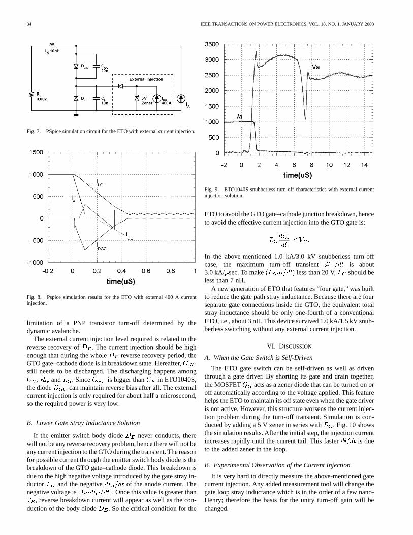
If the emitter switch body diode can be recovered beforethe end of the GTO gate–cathode diode reverse breakdown, theforward current injection will no longer appear. One solutiontherefore is to add an external circuit to the cathode point of theGTO that helps to recover . As shown in Fig. 7, a 400 Acurrent source in parallel with a 5 V Zener diode is used as anexternal current injection.
Fig. 8 shows the simulated waveforms for this case. It is clearthat the reverse recovery of the body diode finishes beforethe end of breakdown, and there is no forward currentinjection into the . A newer generation of ETO1040S hasbeen developed with this concept. They have demonstratedsnubberless turn-off at 1.0 kA/ 3.0kV with a peak instant totalpower of 2.5 MW, or about 200 kW/cmaverage power asshown in Fig. 9. This power constant is close to the theoretical
34 IEEE TRANSACTIONS ON POWER ELECTRONICS, VOL. 18, NO. 1, JANUARY 2003
Fig. 7. PSpice simulation circuit for the ETO with external current injection.
Fig. 8. Pspice simulation results for the ETO with external 400 A currentinjection.
limitation of a PNP transistor turn-off determined by thedynamic avalanche.
The external current injection level required is related to thereverse recovery of . The current injection should be highenough that during the whole reverse recovery period, theGTO gate–cathode diode is in breakdown state. Hereafter,still needs to be discharged. The discharging happens among
, and . Since is bigger than in ETO1040S,the diode can maintain reverse bias after all. The externalcurrent injection is only required for about half a microsecond,so the required power is very low.
B. Lower Gate Stray Inductance Solution
If the emitter switch body diode never conducts, therewill not be any reverse recovery problem, hence there will not beany current injection to the GTO during the transient. The reasonfor possible current through the emitter switch body diode is thebreakdown of the GTO gate–cathode diode. This breakdown isdue to the high negative voltage introduced by the gate stray in-ductor and the negative of the anode current. Thenegative voltage is . Once this value is greater than
, reverse breakdown current will appear as well as the con-duction of the body diode . So the critical condition for the
Fig. 9. ETO1040S snubberless turn-off characteristics with external currentinjection solution.
ETO to avoid the GTO gate–cathode junction breakdown, henceto avoid the effective current injection into the GTO gate is:
In the above-mentioned 1.0 kA/3.0 kV snubberless turn-offcase, the maximum turn-off transient is about3.0 kA/ sec. To make less than 20 V, should beless than 7 nH.
A new generation of ETO that features “four gate,” was builtto reduce the gate path stray inductance. Because there are fourseparate gate connections inside the GTO, the equivalent totalstray inductance should be only one-fourth of a conventionalETO, i.e., about 3 nH. This device survived 1.0 kA/1.5 kV snub-berless switching without any external current injection.
VI. DISCUSSION
A. When the Gate Switch is Self-Driven
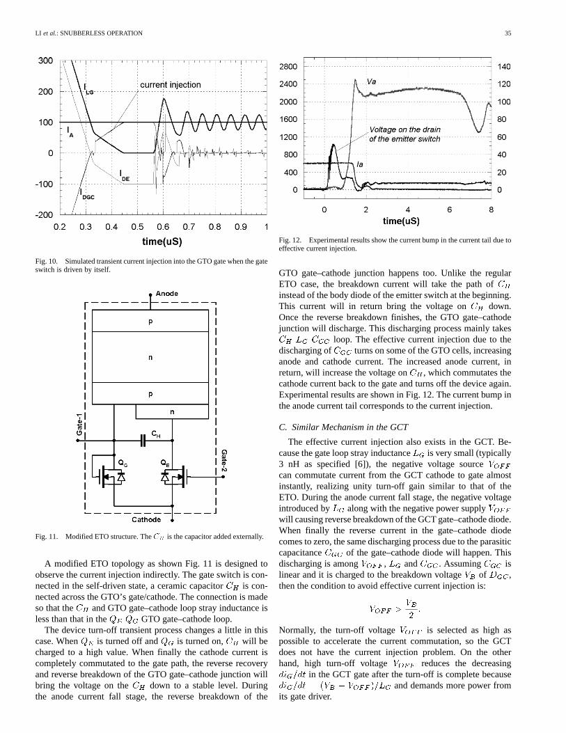
The ETO gate switch can be self-driven as well as driventhrough a gate driver. By shorting its gate and drain together,the MOSFET acts as a zener diode that can be turned on oroff automatically according to the voltage applied. This featurehelps the ETO to maintain its off state even when the gate driveris not active. However, this structure worsens the current injec-tion problem during the turn-off transient. Simulation is con-ducted by adding a 5 V zener in series with . Fig. 10 showsthe simulation results. After the initial step, the injection currentincreases rapidly until the current tail. This faster is dueto the added zener in the loop.
B. Experimental Observation of the Current Injection
It is very hard to directly measure the above-mentioned gatecurrent injection. Any added measurement tool will change thegate loop stray inductance which is in the order of a few nano-Henry; therefore the basis for the unity turn-off gain will bechanged.
LI et al.: SNUBBERLESS OPERATION 35
Fig. 10. Simulated transient current injection into the GTO gate when the gateswitch is driven by itself.
Fig. 11. Modified ETO structure. TheC is the capacitor added externally.
A modified ETO topology as shown Fig. 11 is designed toobserve the current injection indirectly. The gate switch is con-nected in the self-driven state, a ceramic capacitoris con-nected across the GTO’s gate/cathode. The connection is madeso that the and GTO gate–cathode loop stray inductance isless than that in the GTO gate–cathode loop.
The device turn-off transient process changes a little in thiscase. When is turned off and is turned on, will becharged to a high value. When finally the cathode current iscompletely commutated to the gate path, the reverse recoveryand reverse breakdown of the GTO gate–cathode junction willbring the voltage on the down to a stable level. Duringthe anode current fall stage, the reverse breakdown of the
Fig. 12. Experimental results show the current bump in the current tail due toeffective current injection.
GTO gate–cathode junction happens too. Unlike the regularETO case, the breakdown current will take the path ofinstead of the body diode of the emitter switch at the beginning.This current will in return bring the voltage on down.Once the reverse breakdown finishes, the GTO gate–cathodejunction will discharge. This discharging process mainly takes
loop. The effective current injection due to thedischarging of turns on some of the GTO cells, increasinganode and cathode current. The increased anode current, inreturn, will increase the voltage on , which commutates thecathode current back to the gate and turns off the device again.Experimental results are shown in Fig. 12. The current bump inthe anode current tail corresponds to the current injection.
C. Similar Mechanism in the GCT
The effective current injection also exists in the GCT. Be-cause the gate loop stray inductanceis very small (typically3 nH as specified [6]), the negative voltage sourcecan commutate current from the GCT cathode to gate almostinstantly, realizing unity turn-off gain similar to that of theETO. During the anode current fall stage, the negative voltageintroduced by along with the negative power supplywill causing reverse breakdown of the GCT gate–cathode diode.When finally the reverse current in the gate–cathode diodecomes to zero, the same discharging process due to the parasiticcapacitance of the gate–cathode diode will happen. Thisdischarging is among , and . Assuming islinear and it is charged to the breakdown voltageof ,then the condition to avoid effective current injection is:
Normally, the turn-off voltage is selected as high aspossible to accelerate the current commutation, so the GCTdoes not have the current injection problem. On the otherhand, high turn-off voltage reduces the decreasing
in the GCT gate after the turn-off is complete becauseand demands more power from
its gate driver.
36 IEEE TRANSACTIONS ON POWER ELECTRONICS, VOL. 18, NO. 1, JANUARY 2003
D. Current Injection in the MTO [7]
The MOS Turn-Off (MTO) thyristor is another hybridGTO-MOSFET structure that greatly improves the controlof the GTO. Compared to the ETO, the MTO does not havethe emitter switch, but does have a very low gate loop strayinductance . By turning on the gate switch , the GTOgate–cathode diode is shorted and the cathode current can becommutated to the gate if has very low ON impedance,realizing unity turn-off gain.
The same current injection mechanism exists in the MTOduring the turn-off transient. When the anode current is de-creasing, the gate loop stray inductancewill introduce a neg-ative voltage , which will be applied on the GTOreverse gate–cathode PN junction. After the anode current de-crease, the parasitic capacitor of the GTO gate–cathodediode will discharge through the , and loop andeventually introduce forward current injection into the GTOgate–cathode junction.
To avoid an effective minority carrier injection into the GTOgate–cathode junction, the forward voltage on this junctionshould below a critical value so that the junction is not con-ducting. So for the MTO, the condition that can avoid effectivecurrent injection to the GTO gate–cathode junction is:
where is a critical voltage value that causes strong currentinjection.
In the case of nonuniform transient process, even lesscan introduce effective current injection to one
GTO cell.
VII. CONCLUSION
The effective current injection into the GTO gate during theturn-off transient, introduced by the discharging of the GTOemitter junction parasitic capacitor along with the reverse re-covery of the emitter switch body diode, has been found andanalyzed as the failure mechanism for the previous generationsof ETO’s. In the ETO, the gate stray inductance is significantand the high frequency transient process is harmful to deviceoperation. Through a carefully designed external circuit, theabove-mentioned injection can be eliminated and newer genera-tion of the ETO can operate at snubberless condition close to thetheoretical limitation determined by the PNP transistor. FutureETO’s with lower gate stray inductance will have full snubber-less switching capability without any external circuit. This ca-pability will enable the ETO to compete with devices such asIGCT and IGBT in the high power applications.
REFERENCES
[1] Y. Li, A. Q. Huang, and K. Motto, “Experimental and numerical studyof the Emitter Turn-Off thyristor (ETO),”IEEE Trans. Power Electron.,vol. 15, pp. 561–574, May 2000.
[2] P. K. Steimer, H. E. Gruning, J. Werninger, E. Carrol, S. Klaka, andS. Linder, “IGCT—A new emerging technology for high power, lowcost inverters,” inProc. IEEE Ind. Applicat. Soc. Annu. Meeting, NewOrleans, LA, Oct. 5–9, 1997, pp. 1592–1599.
[3] M. Bakowski and U. Gustafsson, “The two basic failure modes in GTOmodeling and experiment,” inProc. ISPSD’95 Conf., pp. 354–368.
[4] H. E. Gruening and A. Zuckerberger, “Hard drive of high power GTOs:Better switching capability obtained through improved gate-units, Anew high power bipolar MOS thyristor,” inProc. IEEE Ind. Applicat.Soc. 31st Annu. Meeting, Oct. 6–10, 1996, pp. 1474–1480.
[5] I. Takata, M. Bessho, K. Koyanagi, M. Akamatsu, K. Satoh, K. Kurachi,and T. Nakagawa, “Snubberless turn-off capability of four-inch 4.5kVGCT thyristor,” inProc. 1998 IEEE Int. Symp. Power Semicond. DevicesICs, 1998, pp. 177–180.
[6] Mitsubishi, GCT data sheet: Tech. Rep., 2002.[7] D. E. Piccone, R. W. De Doncker, J. A. Barrow, and W. H. Tobin, “The
MTO thyristor—A new high power bipolar MOS thyristor,” inProc.IEEE Ind. Applicat. Soc. 31st Annu. Meeting, Oct. 6–10, 1996, pp.1472–1473.
[8] P. K. Steimer, H. E. Gruning, J. Werninger, E. Carrol, S. Klaka, andS. Linder, “IGCT—A new emerging technology for high power, lowcost inverters,” inProc. IEEE Ind. Applicat. Soc. Annu. Meeting, NewOrleans, LA, Oct. 5–9, 1997, pp. 1592–1599.
[9] H. Gruning, et al., “High power hard-driven GTO module for4.5-kV/3-kA snubberless operation,” inProc. PCIM’96 Conf., 1996,pp. 169–183.
[10] Y. Li and A. Q. Huang, “The emitter turn-off thyristor—A new MOS-bipolar high power device,” inProc. 1997 VPEC Sem., Sept. 28–30,1997, pp. 179–183.
[11] A. A. Jaecklin, “Performance limitation of a GTO with near-perfecttechnology,” IEEE Trans. Electron Devices, vol. 39, pp. 1507–1513,June 1992.
[12] J. Oetjen and R. Sittig, “Hybrid 3000A-MOSFET for GTO cascodeswitches,” inProc. ISPSD’97 Conf., 1997, p. 241.
[13] Y. Li, A. Huang, and K. Motto, “Analysis of the snubberless operationof the Emitter Turn-Off Thyristor (ETO),” inProc. 1999 IEEE Int. Conf.Power Electron. Drive Syst., pp. 238–245.
Yuxin Li (M’98) received the B.Eng. degree in radioand electronics engineering from Zhejiang Univer-sity, Hangzhou, China, in 1985, the M.Eng. degree insemiconductor devices from Zhengzhou University,Zhengzhou, China, in 1990, and the Ph.D. degree inpower electronics from Virginia Polytechnic Instituteand State University (Virginia Tech), Blacksburg, in2000.
In 2000, he joined Analog Devices, Inc., SanJose, CA, developing power conversion productsfor battery-powered portable electronics systems.
From 1996 to 2000, he led a research team in Virginia Tech developing theemitter turn-off (ETO) thyristor—a GTO-based high power/speed snubberlessswitch, which has received tremendous attention and funds from governmentagencies and industries. From 1987 to 1996, he worked on the development of300 A/1200 V giant transistors (GTRs) and conducted research and productdevelopment on the Infrared based analog and digital communications. Hehas published over 20 technical papers in referred journals and conferenceproceedings. His current research interests include power management ofbattery-powered systems, computing power solutions, switching mode powersupplies, medium voltage power converters/inverters, and power semiconductordevice characterization.
LI et al.: SNUBBERLESS OPERATION 37
Alex Q. Huang (SM’00) received the B.Sc. degreein electronic engineering from Zheijiang University,China, in 1983, the M.Sc. degree in electronicengineering from Chengdu Institute of Radio Engi-neering, China, in 1986, and the Ph.D. degree fromCambridge University, Cambridge, UK, in 1992.
He is currently an Associate Professor with theCenter for Power Electronics Systems, BradleyDepartment of Electrical and Computer Engineering,Virginia Polytechnic Institute and State University,Blacksburg. Since 1983, he has been involved in the
development of modern power semiconductor devices and power integratedcircuits. He fabricated the first IGBT power device in China in 1985. Whileat Cambridge, he developed a high voltage power IC process to integratepower devices and advanced CMOS devices using conventional CMOStechnology. His current research interests are novel power devices and powerICs, monolithically integrated power managements, high power solid-statedevices, and their applications in electric power regulation and motor drives.He has published more than 80 papers in the international conferences andjournals, and has six U.S. patents.
Dr. Huan received the NSF presidential career award.
Kevin Motto was born in Petersburg, VA, on April 4,1975. He received the B.S. and M.S. degrees in elec-trical engineering from the Virginia Polytechnic In-stitute and State University (Virginia Tech), Blacks-burg, in 1997 and 2000, respectively.
From 1998 to 2000, he was with the Centerfor Power Electronics System, Virginia Tech, as aGraduate Research Assistant. He researched highpower semiconductor devices and their applicationinto medium voltage inverters. Since 2000, hehas been with Northrop Grumman Power/Control
Systems, Sykesville, MD. His work is with high power converters for militaryapplications.
Recommended