Dispositivi e sensori a semiconduttore organico
Annalisa Bonfiglio University of Cagliari, Italy
1: Semiconduttori organici
2: Organic Thin Film Transistors (OTFT)
3: Sensori basati sugli OTFT
Outline prima parte
Proprieta� degli orbitali del Carbonio
Molecole coniugate
Semiconduttori organici: orbitali molecolari e bandgap
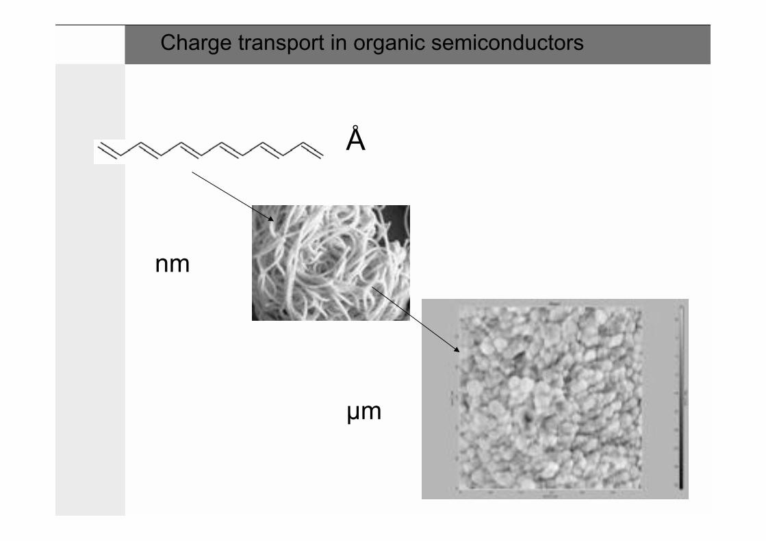
Portatori di carica e trasporto nei semiconduttori organici
Influenza della morfologia sul comportamento elettrico dei film sottili organici
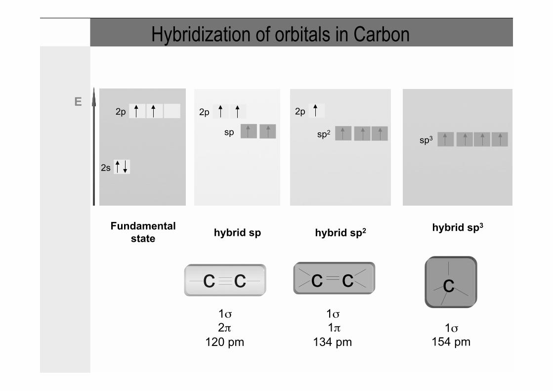
E
2s
2p
Fundamental state
hybrid sp3
sp3
hybrid sp
2p
sp
hybrid sp2
2p
sp2
c c c c c
1σ" 1π "
134 pm 1σ "
154 pm
1σ "2π "
120 pm
Hybridization of orbitals in Carbon
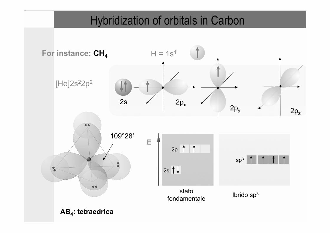
sp3
C = [He]2s22p2
H = 1s1
2s
Ibrido sp3 stato fondamentale
E
2s
2p
2px 2py
AB4: tetraedrica
2pz
For instance: CH4
109°28’
Hybridization of orbitals in Carbon
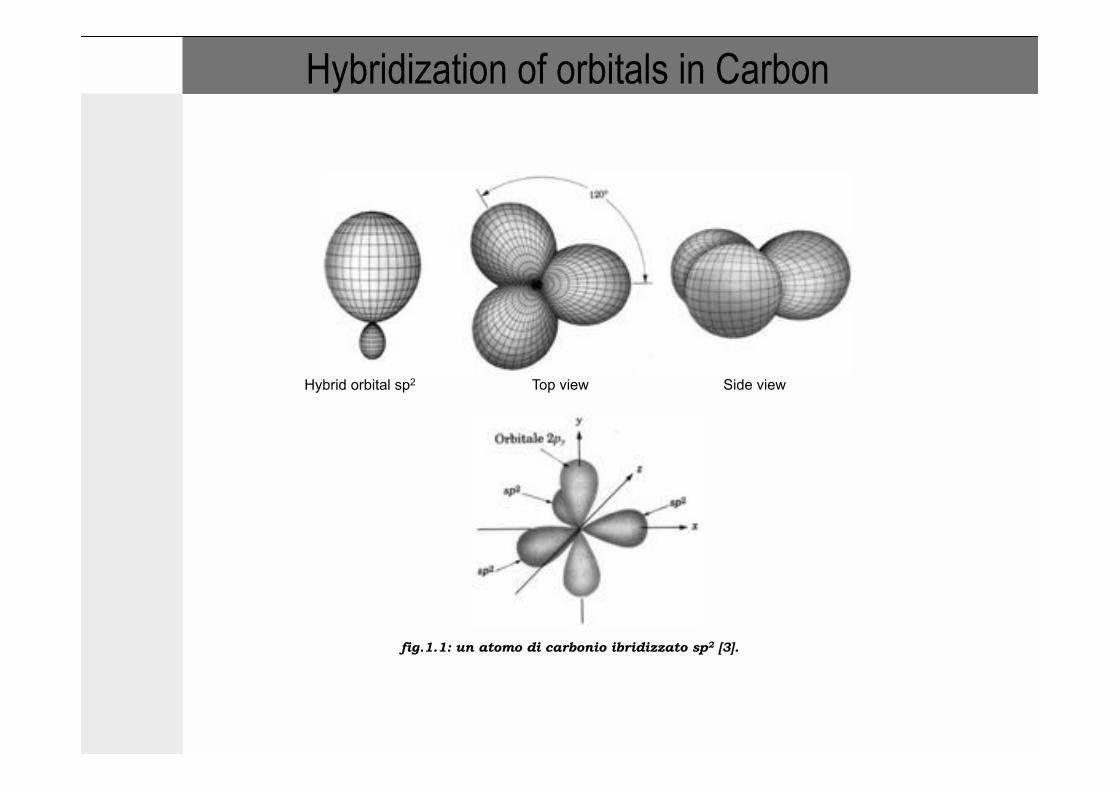
fig.1.1: un atomo di carbonio ibridizzato sp2 [3].
Hybrid orbital sp2 Top view Side view
Hybridization of orbitals in Carbon
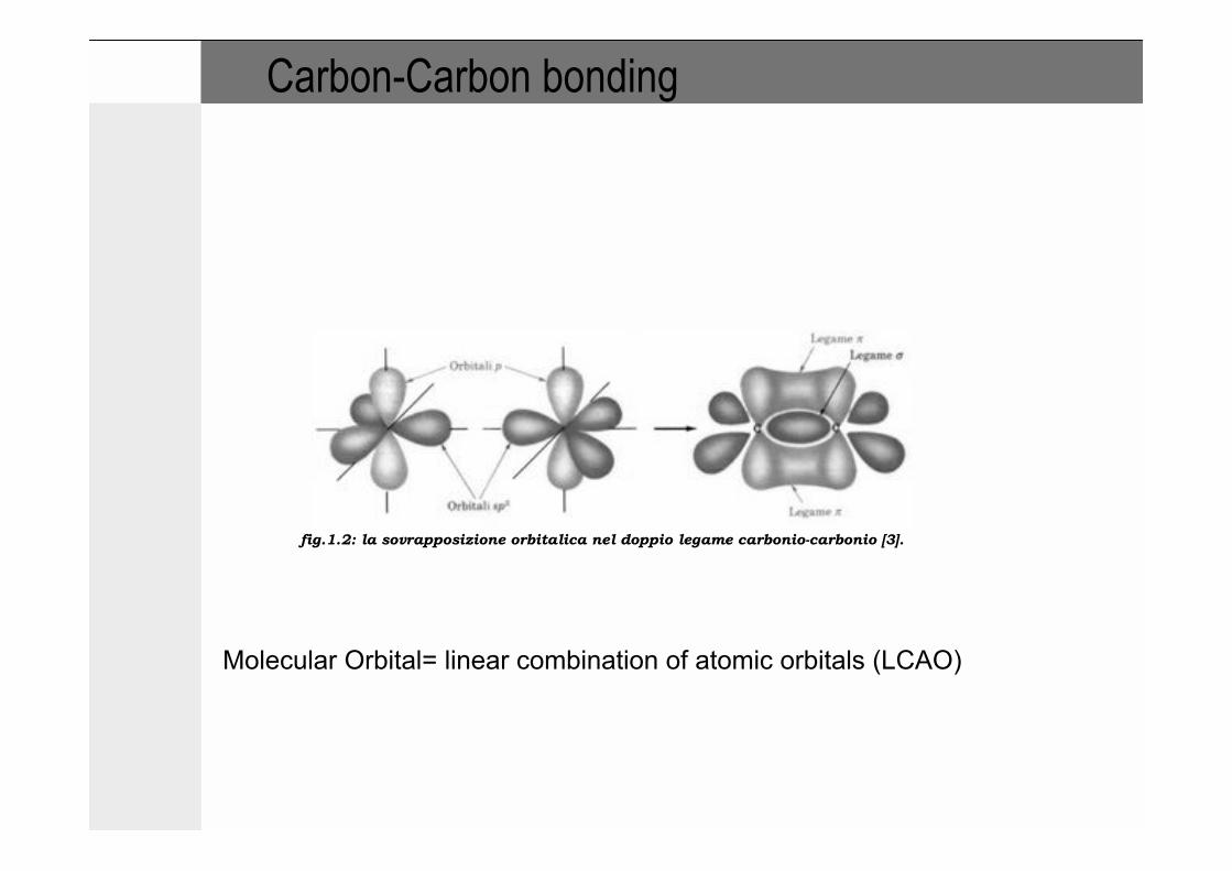
fig.1.2: la sovrapposizione orbitalica nel doppio legame carbonio-carbonio [3].
Molecular Orbital= linear combination of atomic orbitals (LCAO)
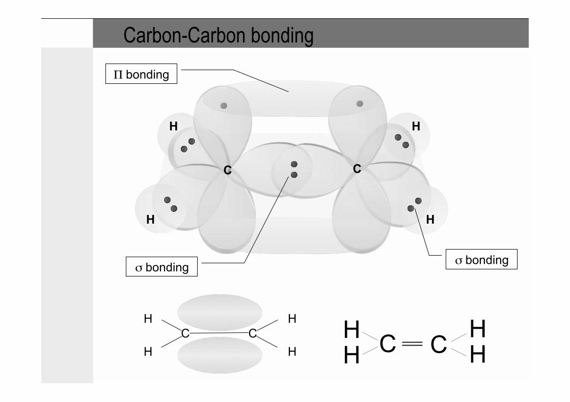
Carbon-Carbon bonding
C C
H
H
H
H
Π bonding"
σ bonding" σ bonding"
C C H
H
H
H H H C C H
H
Carbon-Carbon bonding
C C
H
C
C C
H
C H
H H
H
C C
H
C
C C
H
C H
H H
H
C C
H
C
C C
H
C H
H H
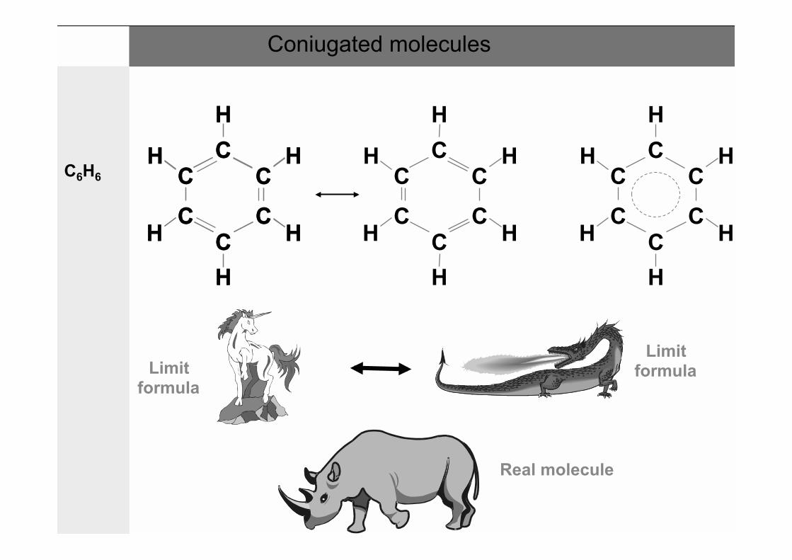
H C6H6
C C
H
C
C C
H
C H
H H
H
Real molecule
Limit formula
Coniugated molecules
Limit formula
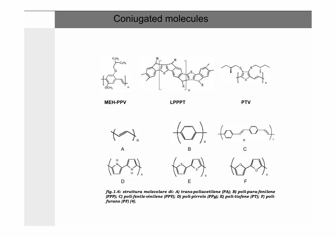
MEH-PPV LPPPT PTV
A B C
D E F fig.1.6: struttura molecolare di: A) trans-poliacetilene (PA); B) poli-para-fenilene (PPP); C) poli-fenile-vinilene (PPV); D) poli-pirrolo (PPy); E) poli-tiofene (PT); F) poli-furano (PF) [4].
Coniugated molecules
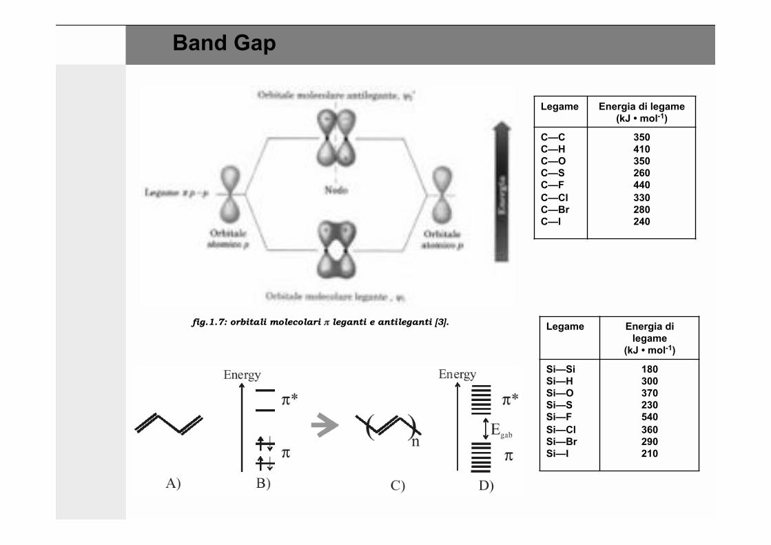
fig.1.7: orbitali molecolari π leganti e antileganti [3].
Band Gap
Legame Energia di legame (kJ • mol-1)
C—C C—H C—O C—S C—F C—Cl C—Br C—I
350 410 350 260 440 330 280 240
Legame Energia di legame
(kJ • mol-1) Si—Si Si—H Si—O Si—S Si—F Si—Cl Si—Br Si—I
180 300 370 230 540 360 290 210
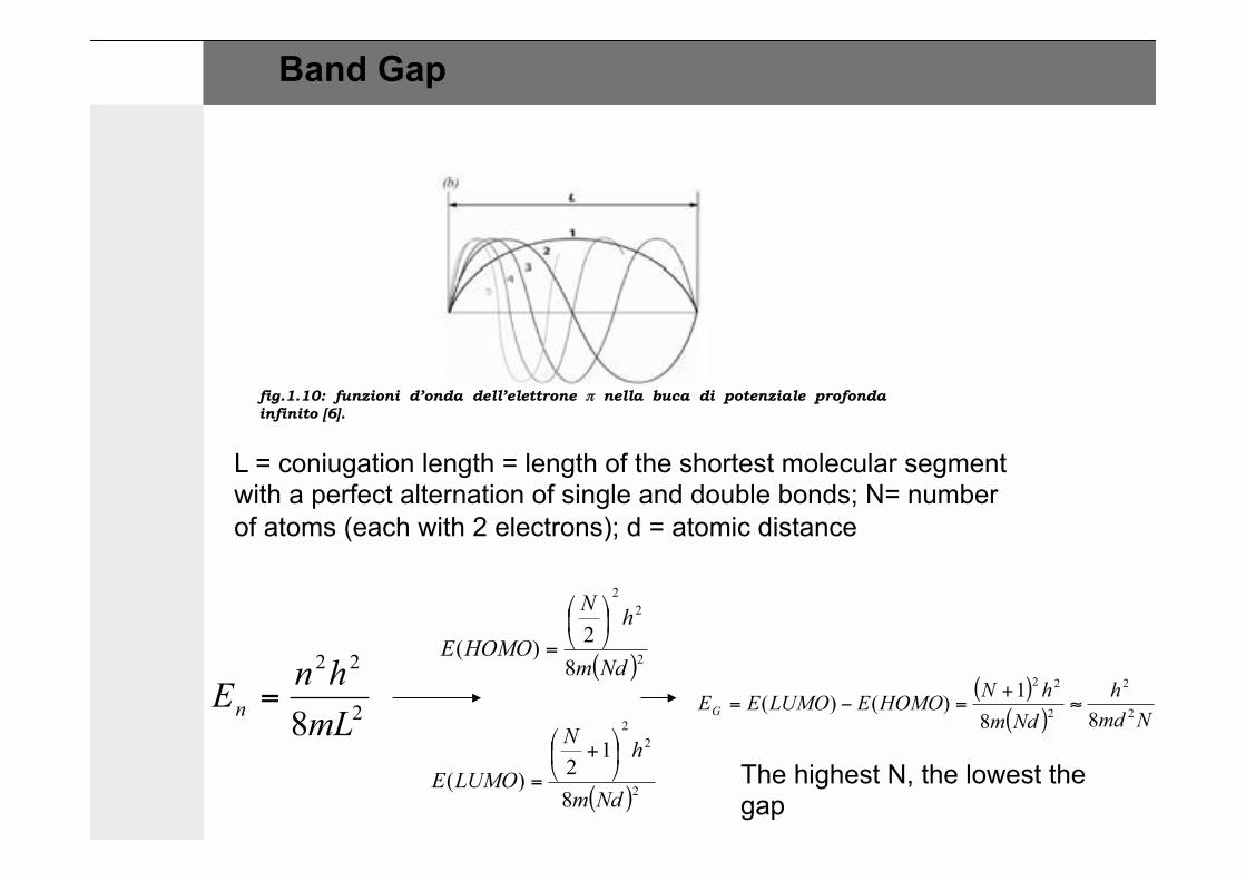
fig.1.10: funzioni d’onda dell’elettrone π nella buca di potenziale profonda infinito [6].
L = coniugation length = length of the shortest molecular segment with a perfect alternation of single and double bonds; N= number of atoms (each with 2 electrons); d = atomic distance
2
22
8mLhnEn =
( )2
22
82)(Ndm
hN
HOMOE!"
#$%
&
=
( )2
22
8
12)(Ndm
hN
LUMOE!"
#$%
& +=
( )( ) Nmd
hNdmhNHOMOELUMOEEG 2
2
2
22
881)()( ≈
+=−=
The highest N, the lowest the gap
Band Gap
Charge transport in organic semiconductors
Å
nm
µm
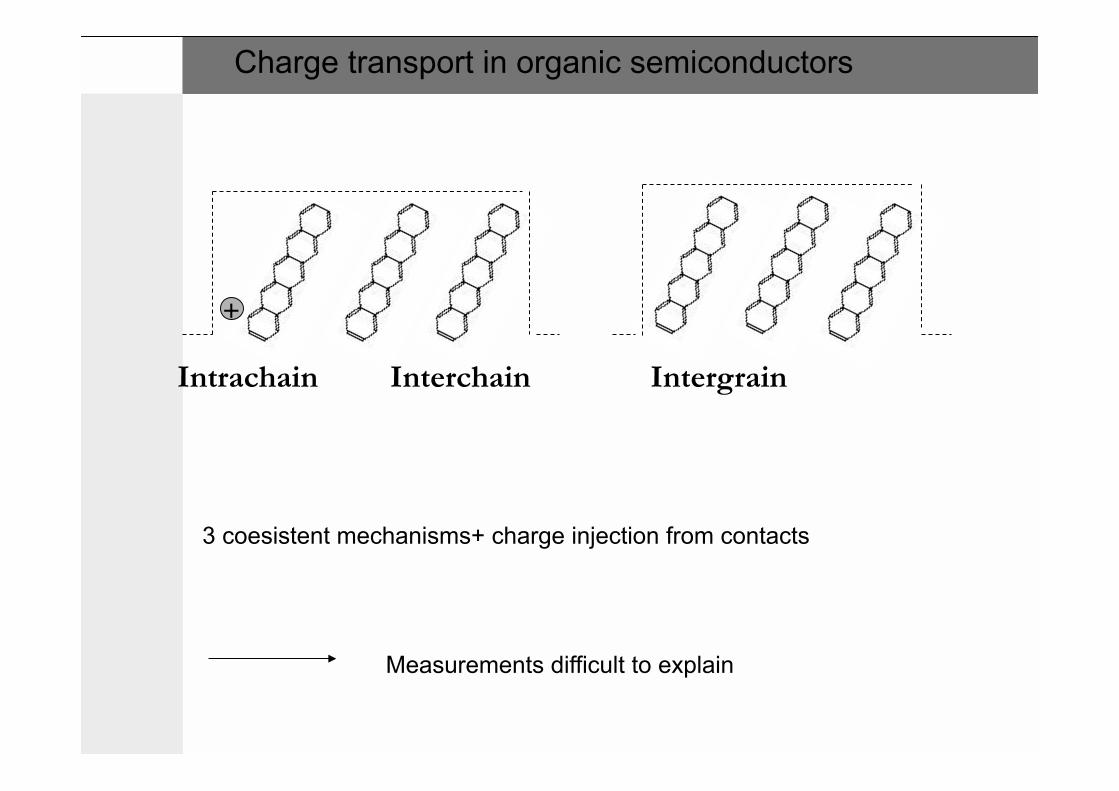
Intrachain Interchain Intergrain
+
3 coesistent mechanisms+ charge injection from contacts
Measurements difficult to explain
Charge transport in organic semiconductors
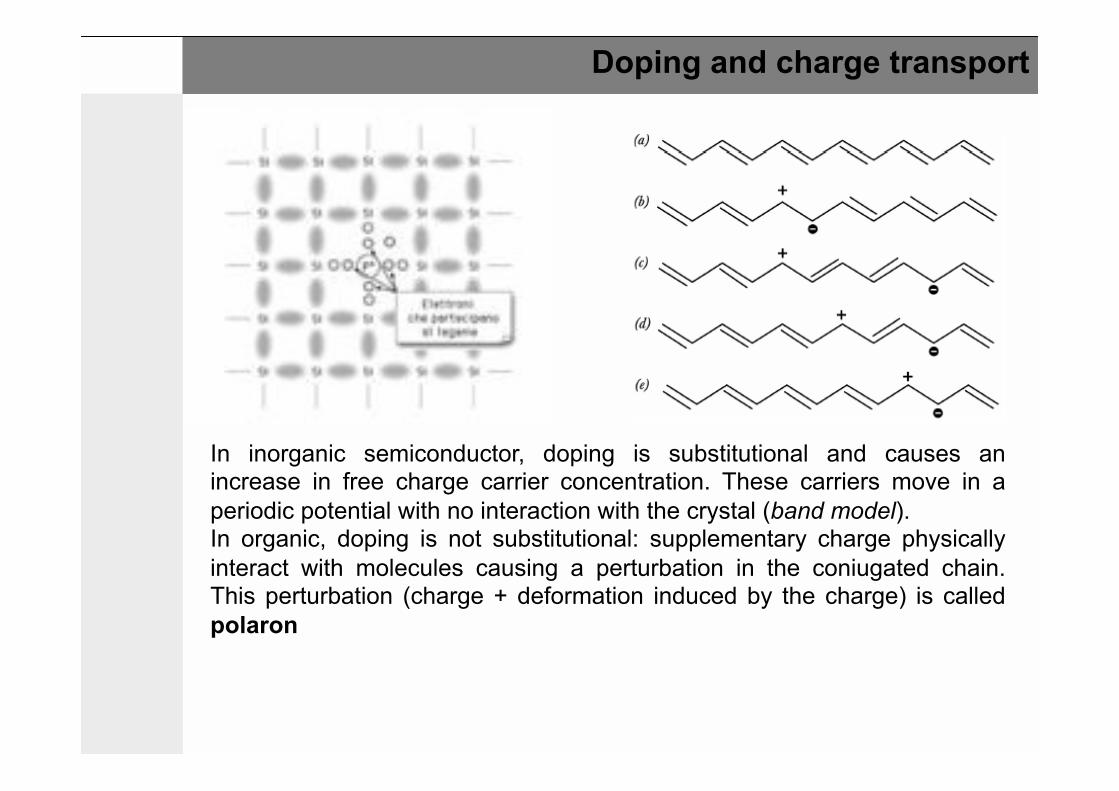
Doping and charge transport
In inorganic semiconductor, doping is substitutional and causes an increase in free charge carrier concentration. These carriers move in a periodic potential with no interaction with the crystal (band model). In organic, doping is not substitutional: supplementary charge physically interact with molecules causing a perturbation in the coniugated chain. This perturbation (charge + deformation induced by the charge) is called polaron
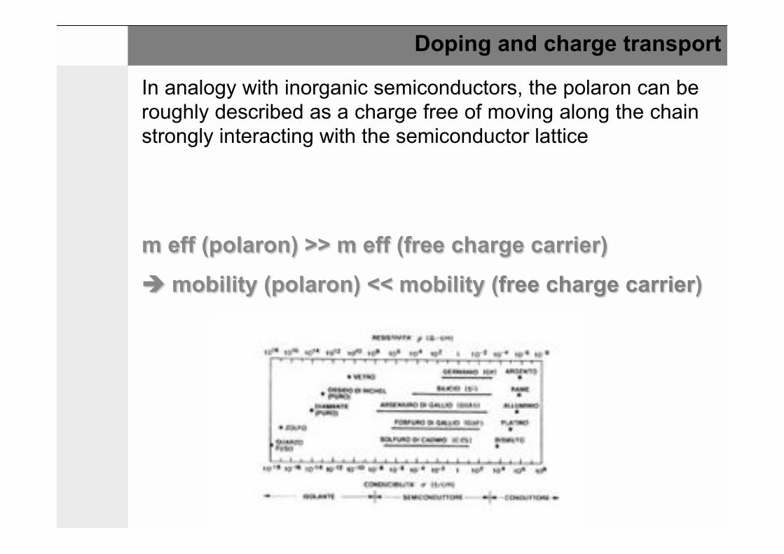
In analogy with inorganic semiconductors, the polaron can be roughly described as a charge free of moving along the chain strongly interacting with the semiconductor lattice
m eff (polaron) >> m eff (free charge carrier)
! mobility (polaron) << mobility (free charge carrier)
Doping and charge transport
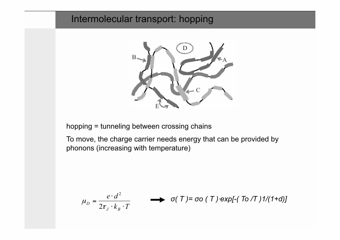
Intermolecular transport: hopping
hopping = tunneling between crossing chains
To move, the charge carrier needs energy that can be provided by phonons (increasing with temperature)
TkdeBJ
D ⋅⋅
⋅=
τµ
2
2σ( T )= σo ( T )⋅exp[-( To /T )1/(1+d)]
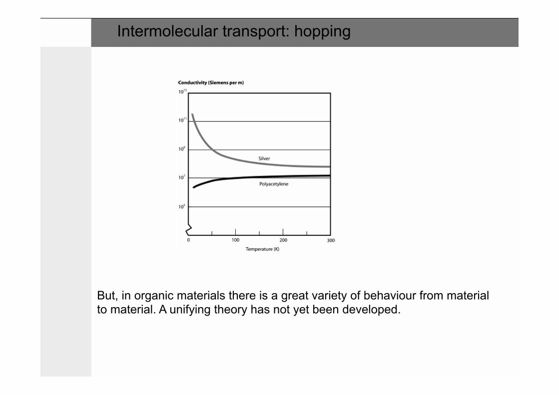
But, in organic materials there is a great variety of behaviour from material to material. A unifying theory has not yet been developed.
Intermolecular transport: hopping
Materials for “Plastic Electronics”
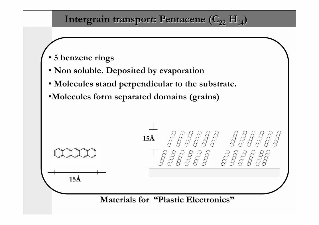
Intergrain transport: Pentacene (C22 H14)
• 5 benzene rings • Non soluble. Deposited by evaporation
• Molecules stand perpendicular to the substrate. • Molecules form separated domains (grains)
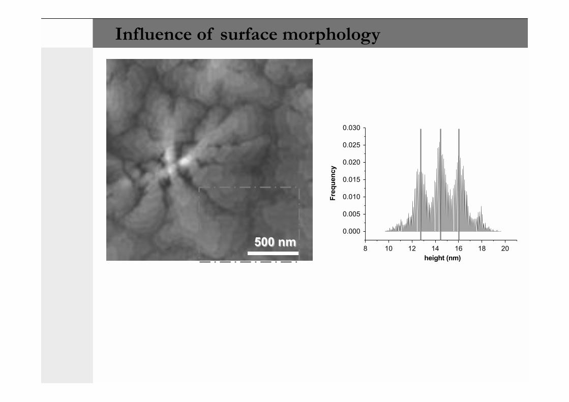
15Å
15Å
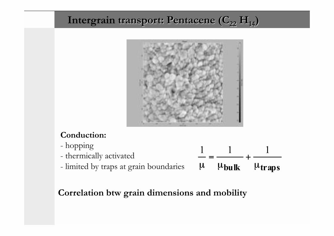
Conduction: - hopping - thermically activated - limited by traps at grain boundaries
Correlation btw grain dimensions and mobility
trapsbulk µµµ
111+=
Intergrain transport: Pentacene (C22 H14)
8 10 12 14 16 18 20
0.000
0.005
0.010
0.015
0.020
0.025
0.030
Freq
uenc
y
height (nm)
500 nm
Influence of surface morphology
1 µm 1 µm
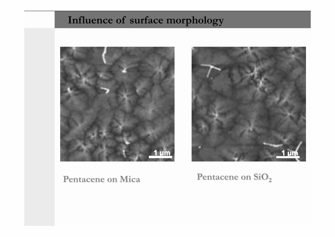
Pentacene on Mica Pentacene on SiO2
Influence of surface morphology
1 µm
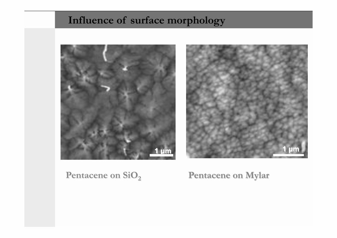
Pentacene on SiO2 Pentacene on Mylar
1 µm
Influence of surface morphology
Outline seconda parte
Organic Thin Film Transistors (OTFTs)
Contatti metallo-semiconduttore organico
Comportamento elettrico degli OTFT
Modello elettrico del dispositivo
Tecnologia
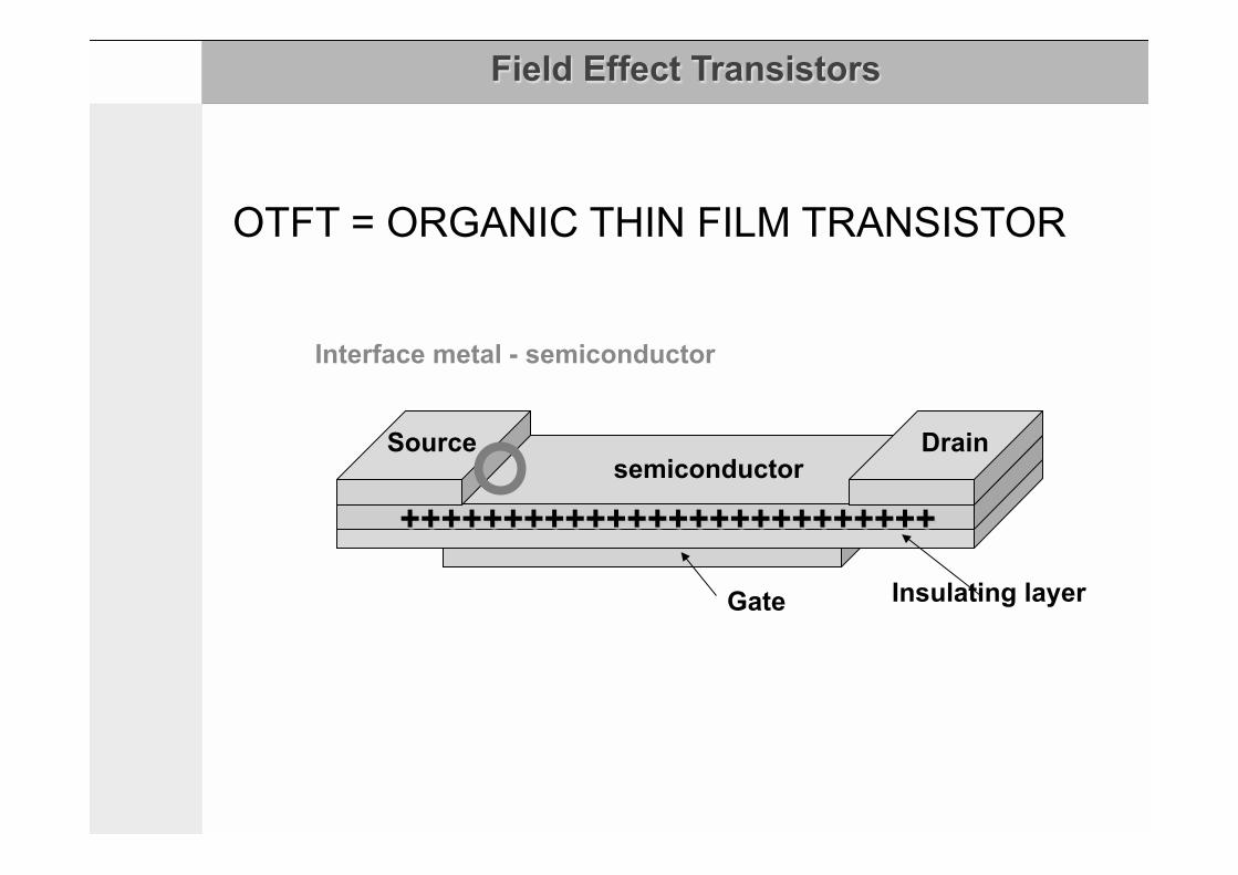
++++++++++++++++++++++++++
Source Drain semiconductor
Insulating layer
OTFT = ORGANIC THIN FILM TRANSISTOR
Field Effect Transistors
Interface metal - semiconductor
Gate
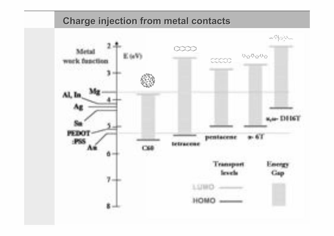
Charge injection from metal contacts
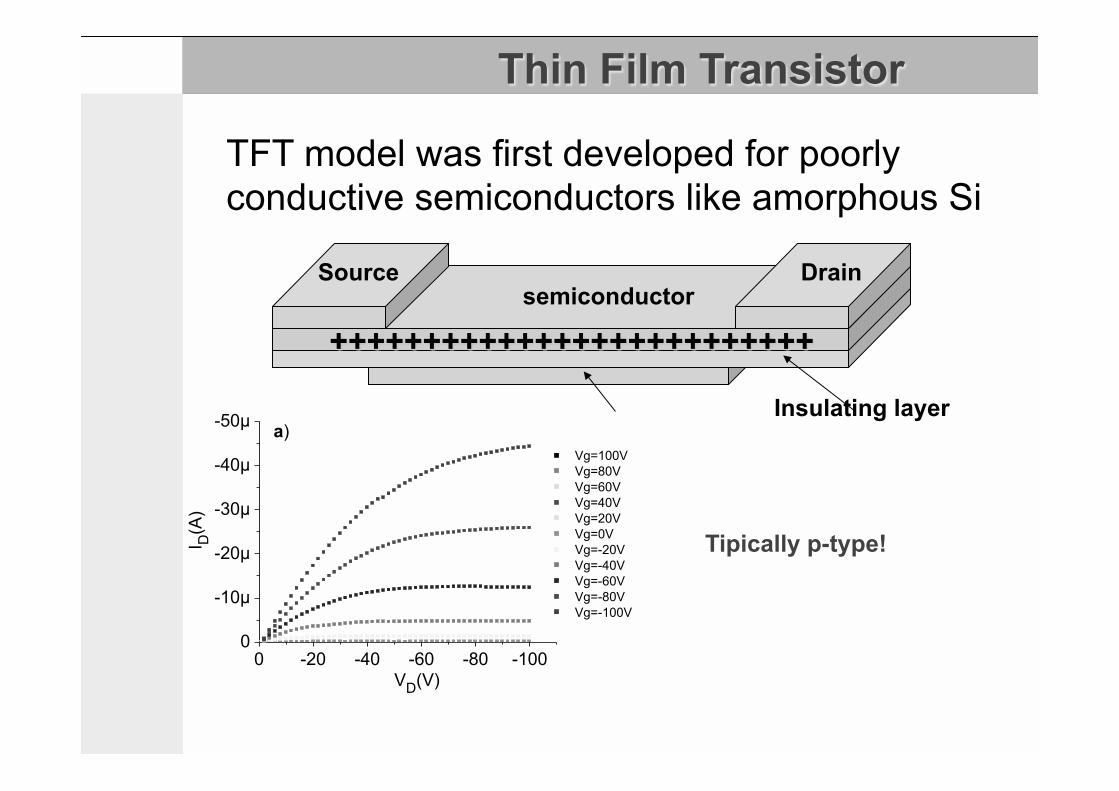
TFT model was first developed for poorly conductive semiconductors like amorphous Si
Tipically p-type!
Thin Film Transistor
++++++++++++++++++++++++++
Source Drain semiconductor
Insulating layer
0 -20 -40 -60 -80 -1000
-10µ
-20µ
-30µ
-40µ
-50µ a) Vg=100V Vg=80V Vg=60V Vg=40V Vg=20V Vg=0V Vg=-20V Vg=-40V Vg=-60V Vg=-80V Vg=-100V
I D(A
)
VD(V)
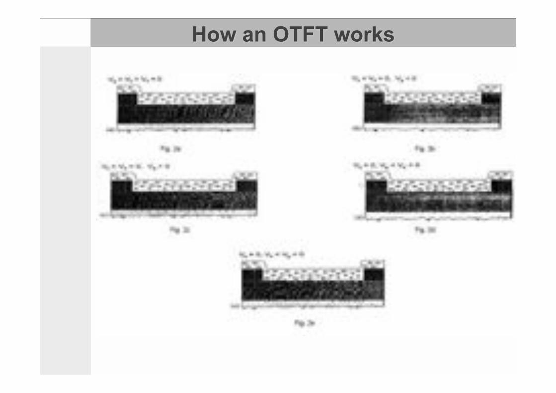
How an OTFT works
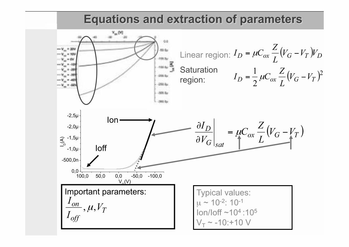
Typical values: µ ~ 10-2: 10-1
Ion/Ioff ~104 :105
VT ~ -10:+10 V
Linear region:
Saturation region:
( )
( )221
TGoxD
DTGoxD
VVLZ
CI
VVVLZ
CI
−=
−=
µ
µ
Toff
on VII ,,µ
Important parameters:
( )TGoxsatG
D VVLZ
CVI
−=∂
∂µ
100,0 50,0 0,0 -50,0 -100,00,0
-500,0n
-1,0µ
-1,5µ
-2,0µ
-2,5µ Bottom Contact Au electrodesVt=-7.5Vµ=5.2x10⁻³cm2/VsZ/L=53
I D(A
)
VG(V)
Ioff
Ion
Equations and extraction of parameters
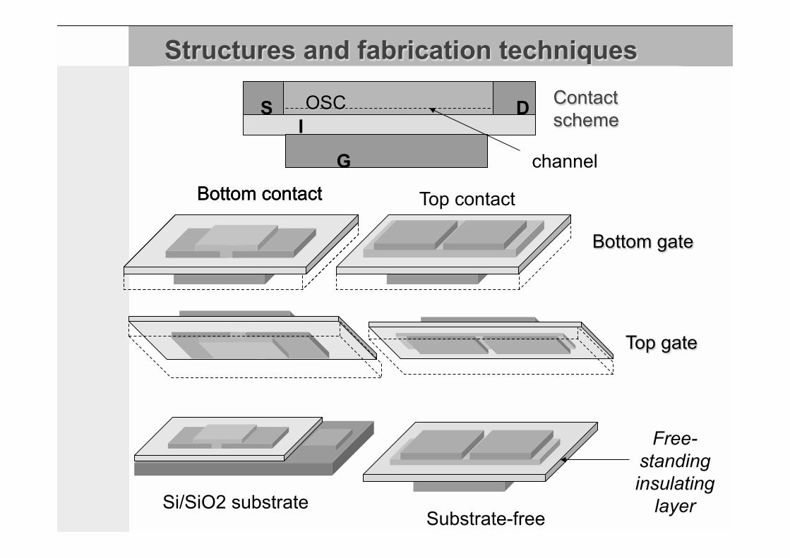
Structures and fabrication techniques
Bottom gate
Top gate
Si/SiO2 substrate Substrate-free
Free-standing insulating
layer
OSC S D
G
I Contact scheme
channel
Top contact Bottom contact Bottom contact Bottom contact
OSC S D
G
I Contact scheme
channel
OSC
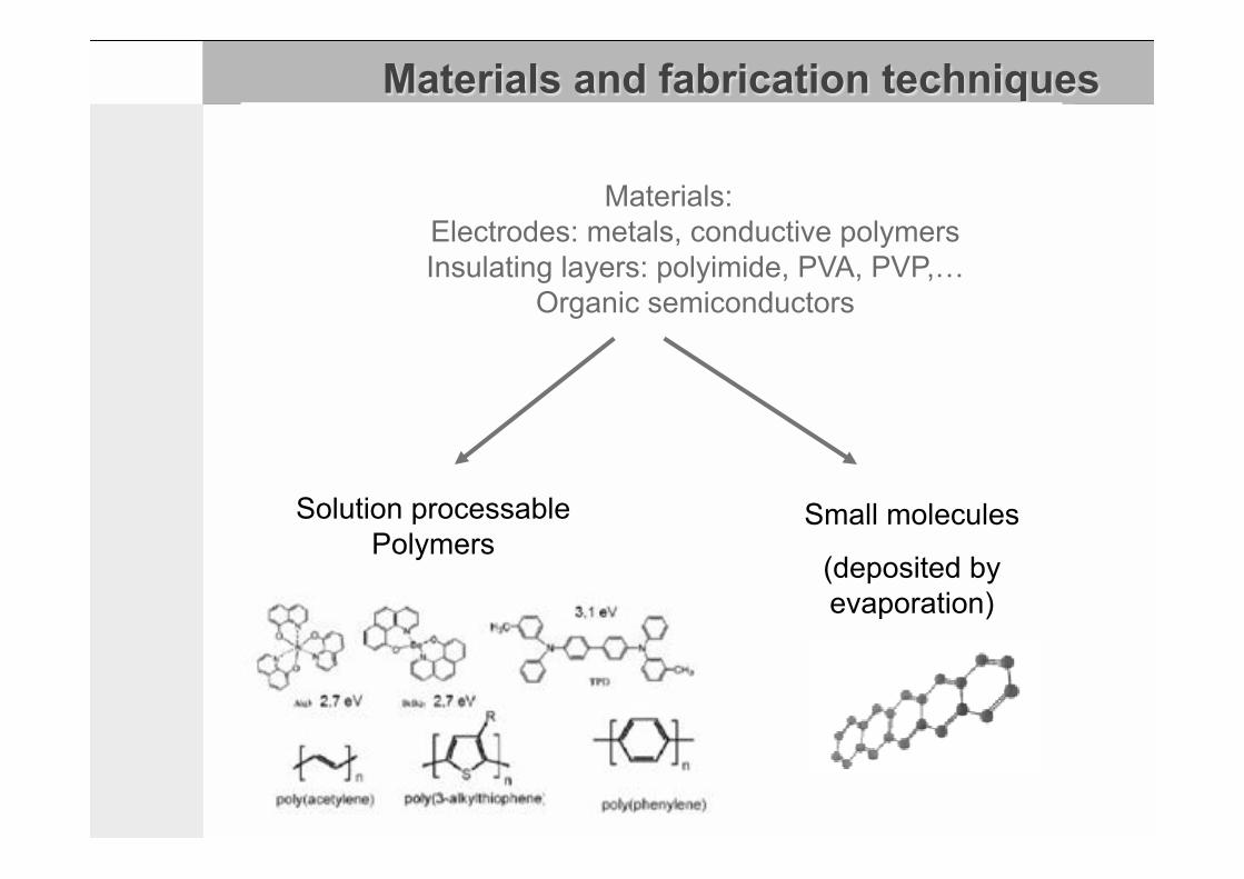
Materials and fabrication techniques OSC
S D
G
I Contact scheme
channel
Materials: Electrodes: metals, conductive polymers Insulating layers: polyimide, PVA, PVP,…
Organic semiconductors
Solution processable Polymers
Small molecules
(deposited by evaporation)
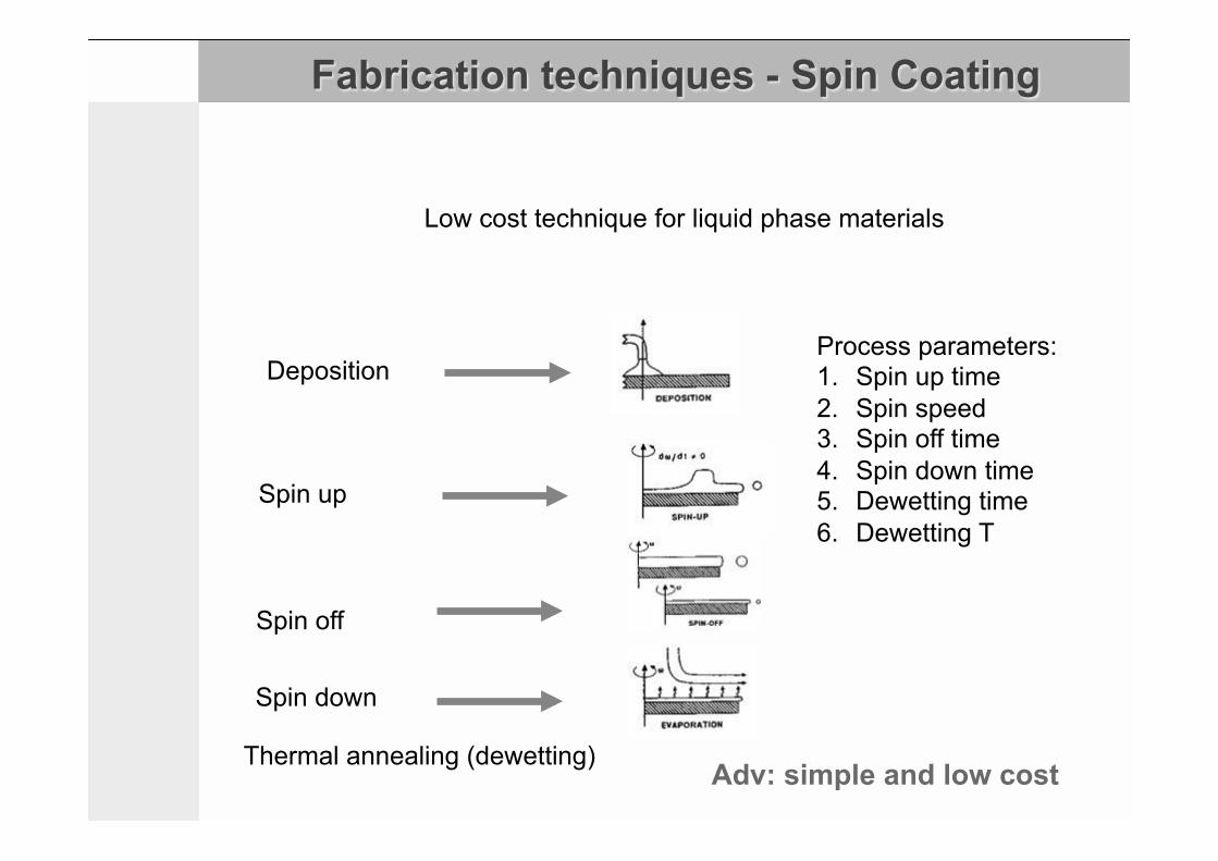
Low cost technique for liquid phase materials
Deposition
Spin up
Spin off
Spin down
Process parameters: 1. Spin up time 2. Spin speed 3. Spin off time 4. Spin down time 5. Dewetting time 6. Dewetting T
Thermal annealing (dewetting) Adv: simple and low cost
Fabrication techniques - Spin Coating
1) 2)
3) 4)
5) 6)
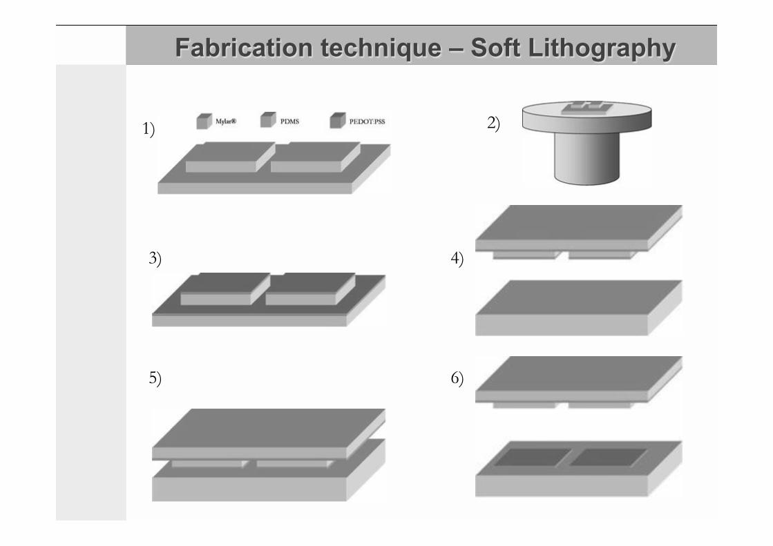
Fabrication technique – Soft Lithography
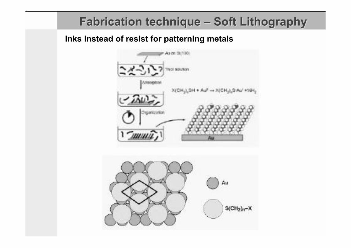
Inks instead of resist for patterning metals
Fabrication technique – Soft Lithography
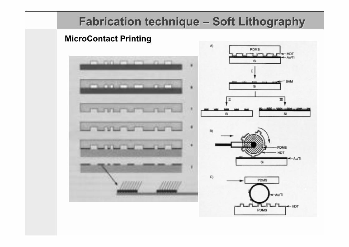
MicroContact Printing
Fabrication technique – Soft Lithography
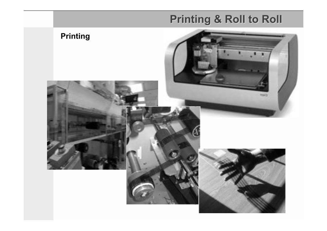
Printing & Roll to Roll Printing
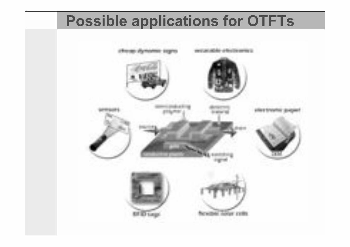
Possible applications for OTFTs
Outline terza parte
Sensori per variabili meccaniche
Sensori per variabili chimiche: ISOFET
Prospettive applicative
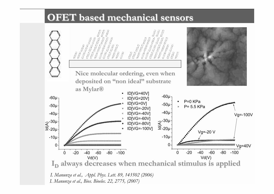
OFET based mechanical sensors
0 -20 -40 -60 -80 -100
0
-10µ
-20µ
-30µ
-40µ
-50µ
-60µID[VG=40V]ID[VG=20V]ID[VG=0V]ID[VG=-20V]ID[VG=-40V]ID[VG=-60V]ID[VG=-80V]ID[VG=-100V]Id
(A)
Vd(V)0 -20 -40 -60 -80 -100
0
-10µ
-20µ
-30µ
-40µ
-50µ
-60µ P=0 KPa P= 5.5 KPa
Id(A
)Vd(V)
Vg=-100V
Vg=40V
Vg=-20 V
Nice molecular ordering, even when deposited on “non ideal” substrate as Mylar®
I. Manunza et al., Appl. Phys. Lett. 89, 143502 (2006) I. Manunza et al., Bios. Bioelec. 22, 2775, (2007)
ID always decreases when mechanical stimulus is applied
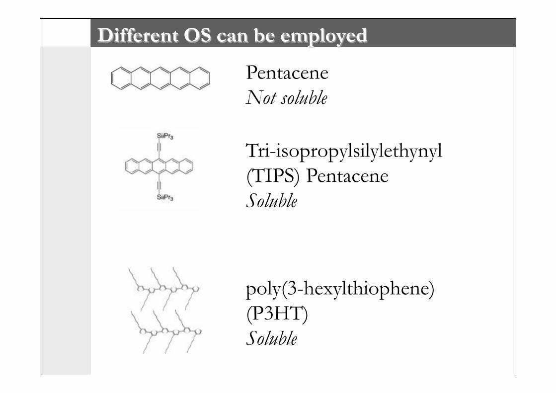
Different OS can be employed
Tri-isopropylsilylethynyl (TIPS) Pentacene Soluble
Pentacene Not soluble
poly(3-hexylthiophene) (P3HT) Soluble
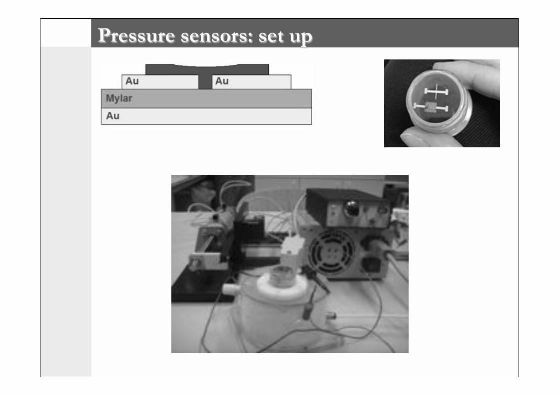
Pressure sensors: set up
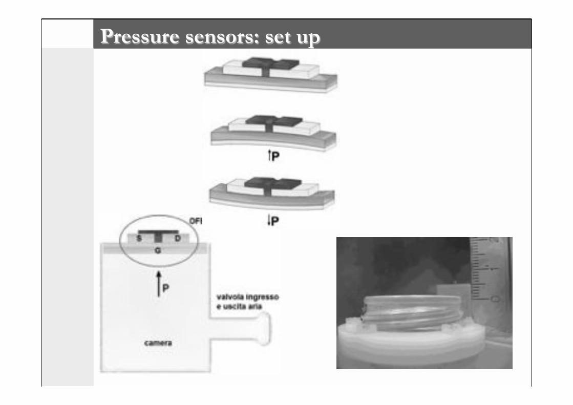
Pressure sensors: set up
Pressure Sensors: pentacene
100 50 0 -50 -100
0.0
0.2
0.4
0.6
0.8
1.0 P=0KPa P=3.7KPa P=-4.2KPa
I D n
orm
aliz
ed fo
r P=0
kP
a
VG(V)
0 100 200 300 400 500 600
-450n
-375n
-300n
-225n
-150n
0.0
4.0
ID
I D[A
]
Time[s]
VG=-40VVD=-10V
Pressure
Pre
ssur
e[K
Pa]
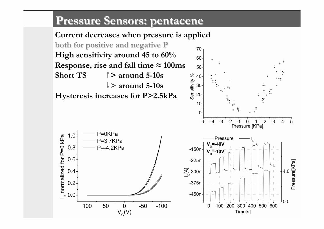
Current decreases when pressure is applied both for positive and negative P High sensitivity around 45 to 60% Response, rise and fall time ≈ 100ms Short TS > around 5-10s
> around 5-10s Hysteresis increases for P>2.5kPa
-5 -4 -3 -2 -1 0 1 2 3 4 5
0
10
20
30
40
50
60
70
Sens
itivi
ty %
Pressure [KPa]
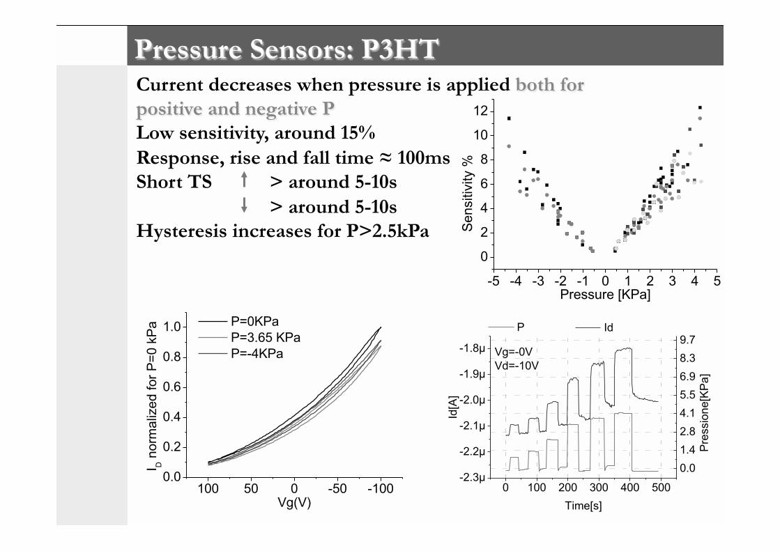
Pressure Sensors: P3HT
100 50 0 -50 -1000.0
0.2
0.4
0.6
0.8
1.0 P=0KPa P=3.65 KPa P=-4KPa
I D n
orm
aliz
ed fo
r P=0
kP
a
Vg(V)0 100 200 300 400 500
-2.3µ
-2.2µ
-2.1µ
-2.0µ
-1.9µ
-1.8µ
0.0
1.4
2.8
4.1
5.5
6.9
8.3
9.7 Id
Id[A
]
Time[s]
Vg=-0VVd=-10V
P
Pre
ssio
ne[K
Pa]
Current decreases when pressure is applied both for positive and negative P Low sensitivity, around 15% Response, rise and fall time ≈ 100ms Short TS > around 5-10s
> around 5-10s Hysteresis increases for P>2.5kPa
-5 -4 -3 -2 -1 0 1 2 3 4 5
0
2
4
6
8
10
12
Sen
sitiv
ity %
Pressure [KPa]
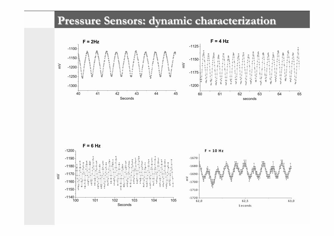
Pressure Sensors: dynamic characterization
40 41 42 43 44 45
-1300
-1250
-1200
-1150
-1100
F = 2Hz
mV
Seconds60 61 62 63 64 65
-1200
-1175
-1150
-1125F = 4 Hz
mV
seconds
100 101 102 103 104 105-1140
-1150
-1160
-1170
-1180
-1190
-1200
mV
F = 6 Hz
Seconds62,0 62,5 63,0
'1720
'1710
'1700
'1690
'1680
'1670
F "= "10"Hz
mV
S econds
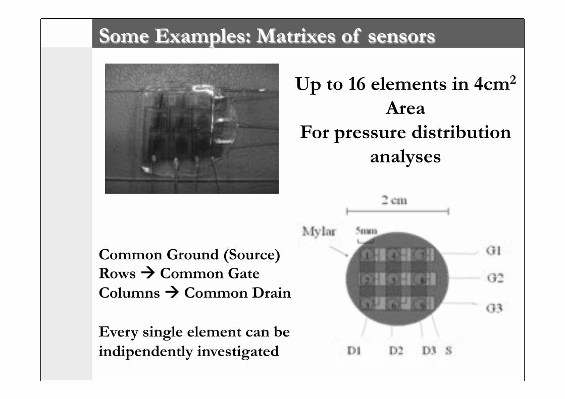
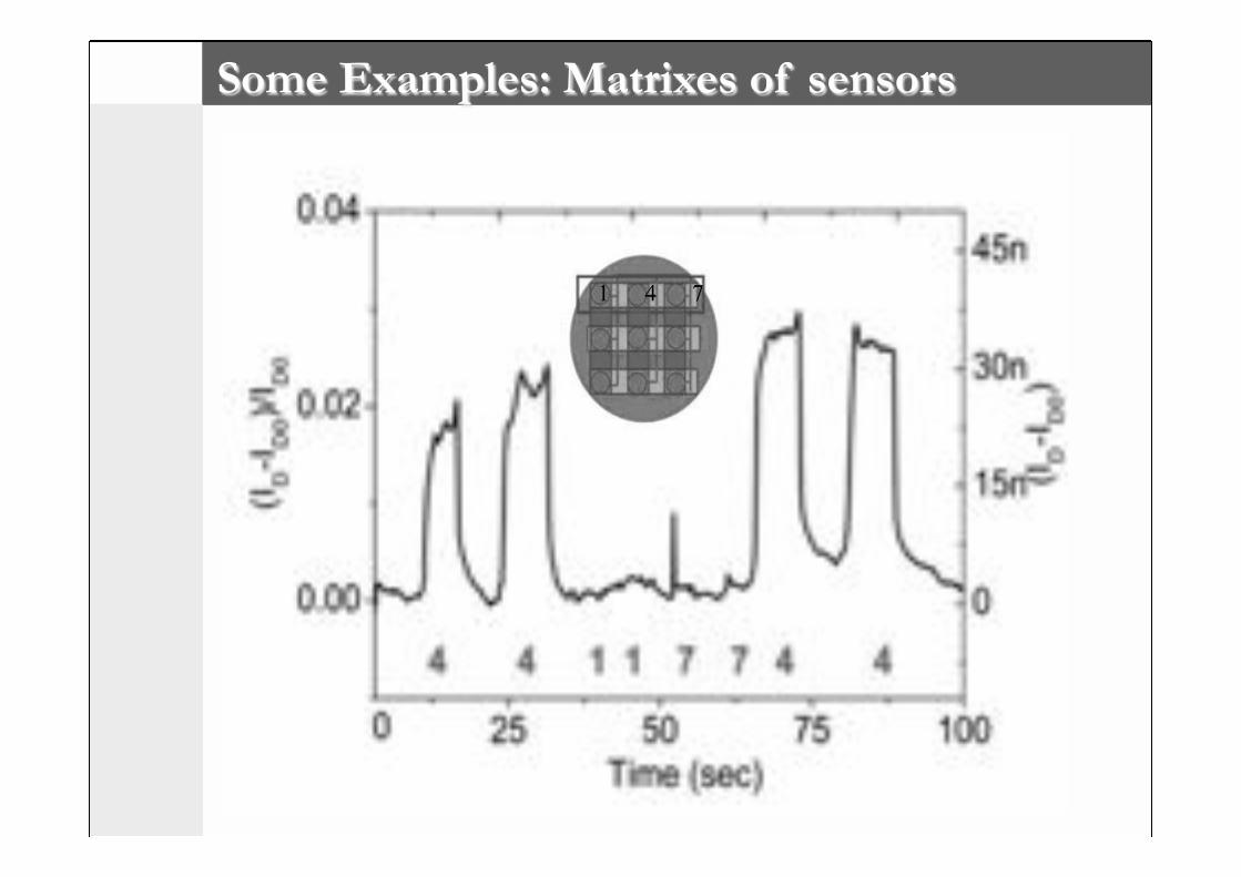
Some Examples: Matrixes of sensors
Up to 16 elements in 4cm2 Area
For pressure distribution analyses
Common Ground (Source) Rows " Common Gate Columns " Common Drain Every single element can be indipendently investigated
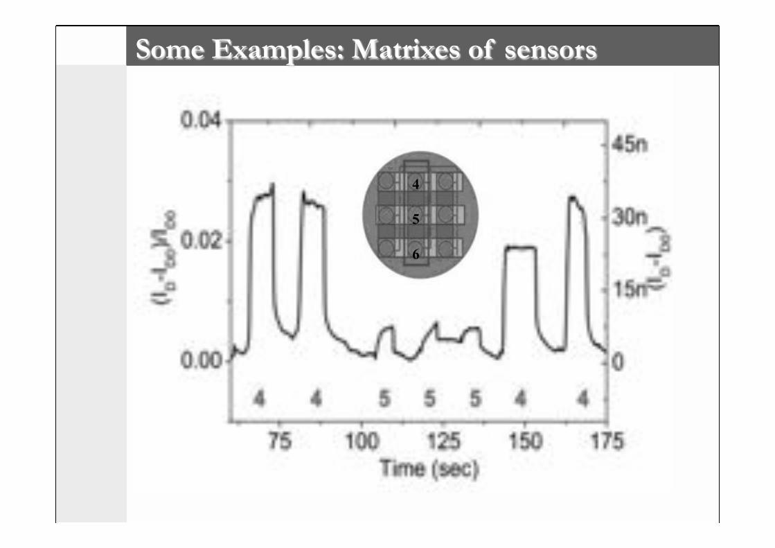
Some Examples: Matrixes of sensors
4 5 6
Some Examples: Matrixes of sensors
1 4 7
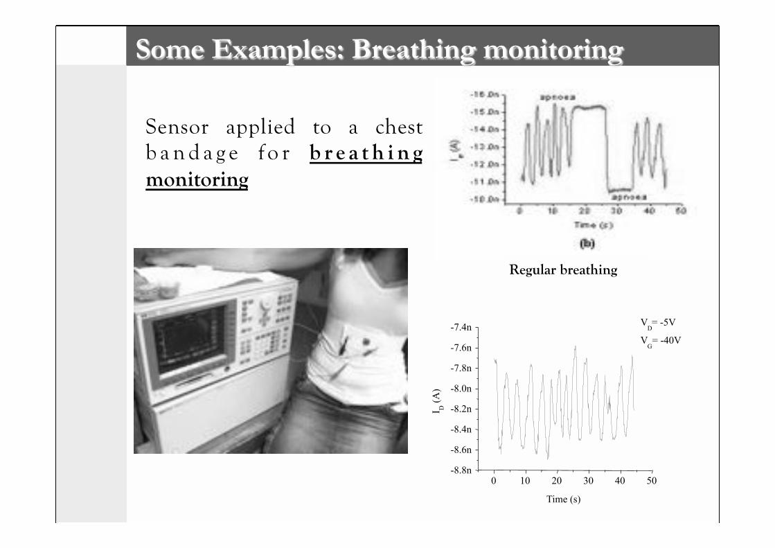
Some Examples: Breathing monitoring
Sensor applied to a chest b a n d a g e f o r b r e a t h i n g monitoring
0 10 20 30 40 50 -8.8n -8.6n -8.4n -8.2n -8.0n -7.8n -7.6n -7.4n
I D (A
)
Time (s)
V D = -5V
V G = -40V
Regular breathing
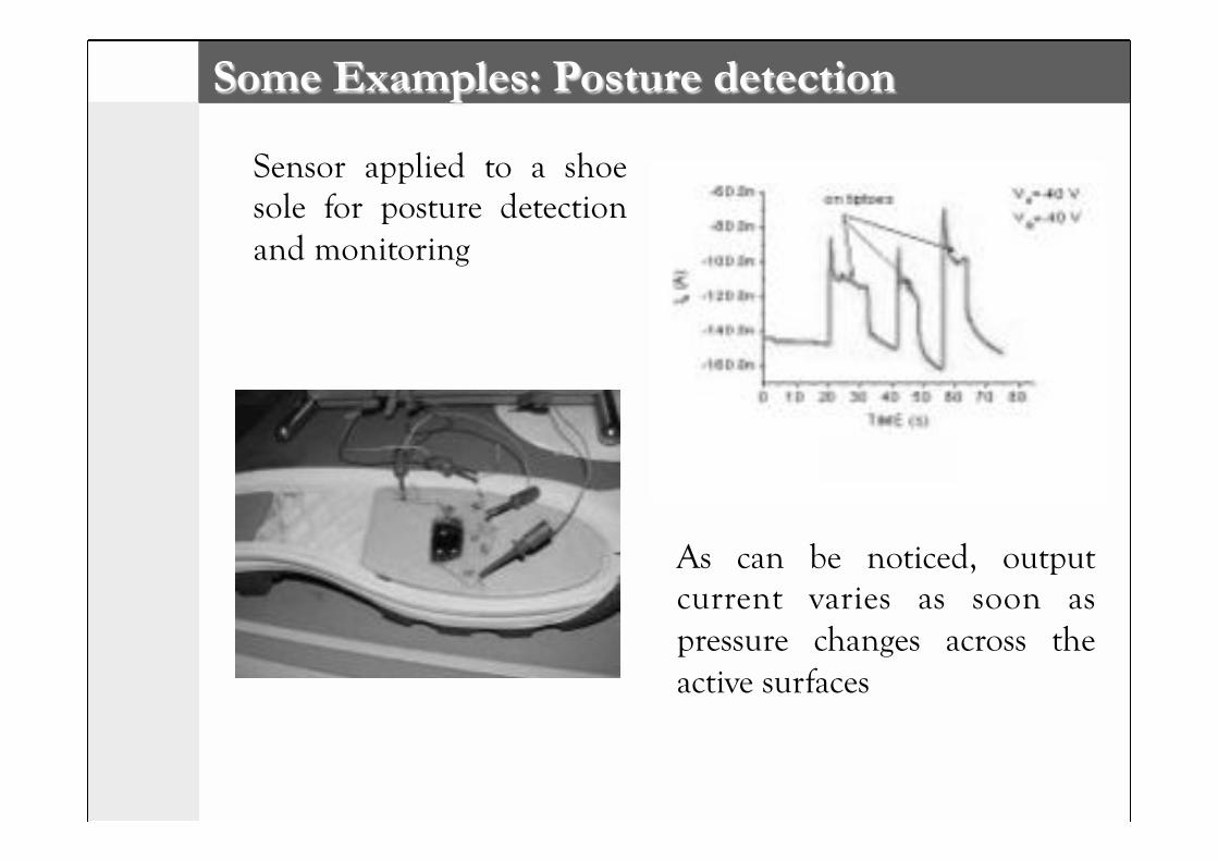
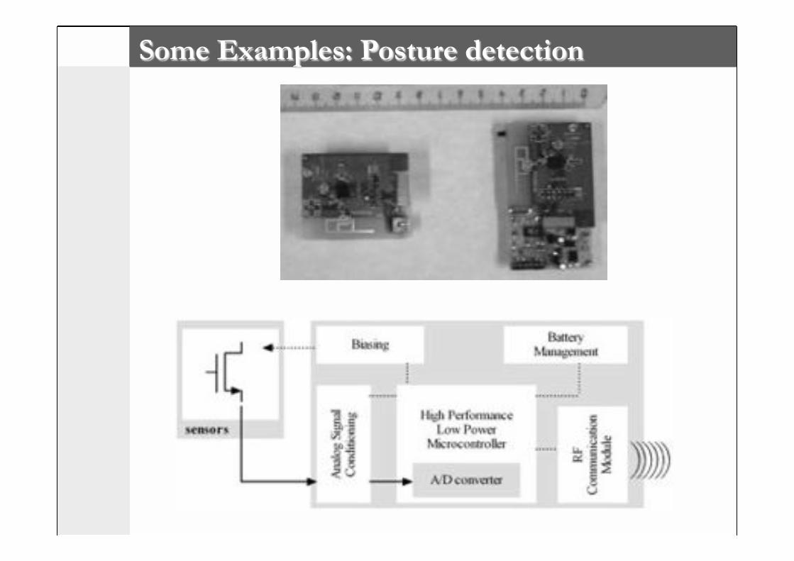
Some Examples: Posture detection
Sensor applied to a shoe sole for posture detection and monitoring
As can be noticed, output current varies as soon as pressure changes across the active surfaces
Some Examples: Posture detection
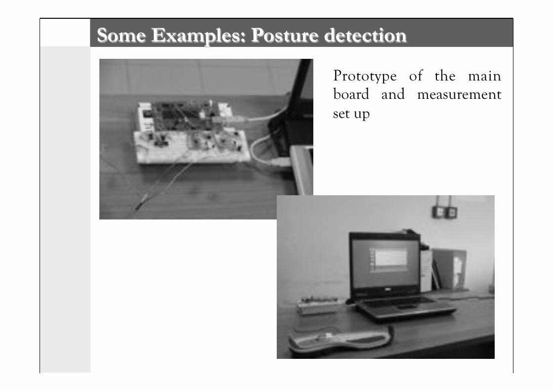
Prototype of the main board and measurement set up
Some Examples: Posture detection
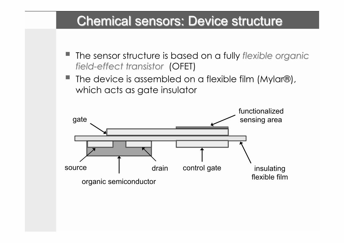
Chemical sensors: Device structure
# The sensor structure is based on a fully flexible organic field-effect transistor (OFET)
# The device is assembled on a flexible film (Mylar®), which acts as gate insulator
source drain
organic semiconductor
gate
insulating flexible film
control gate
functionalized sensing area
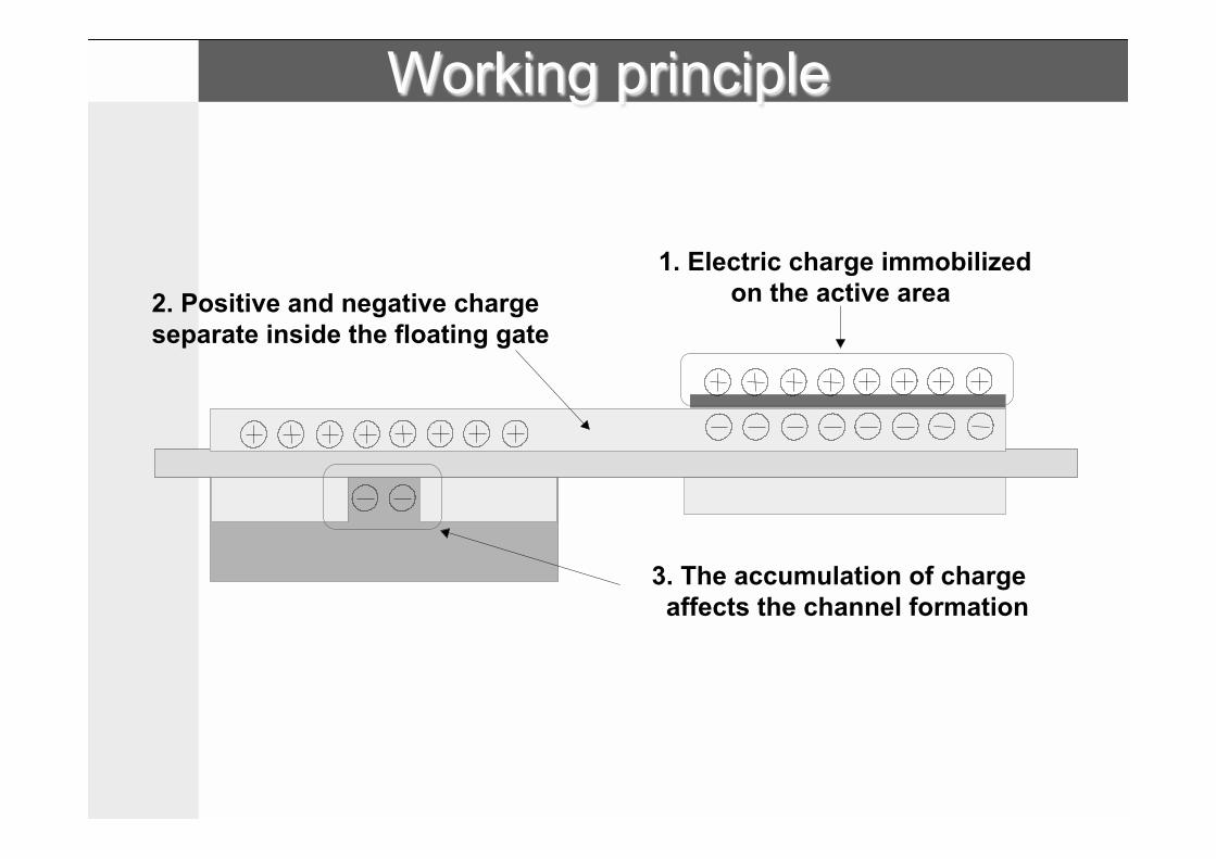
Working principle
1. Electric charge immobilized on the active area 2. Positive and negative charge
separate inside the floating gate
3. The accumulation of charge affects the channel formation
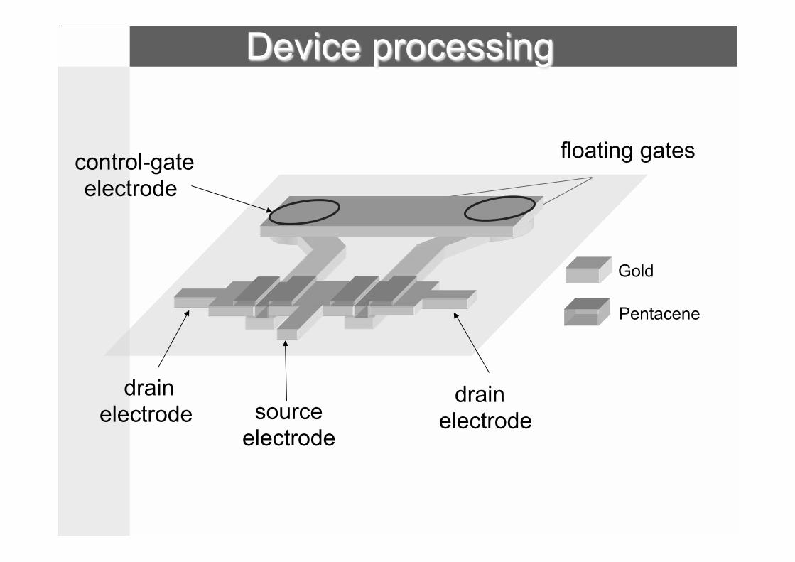
floating gates
Gold
Device processing
Pentacene
drain electrode
control-gate electrode
source electrode
drain electrode
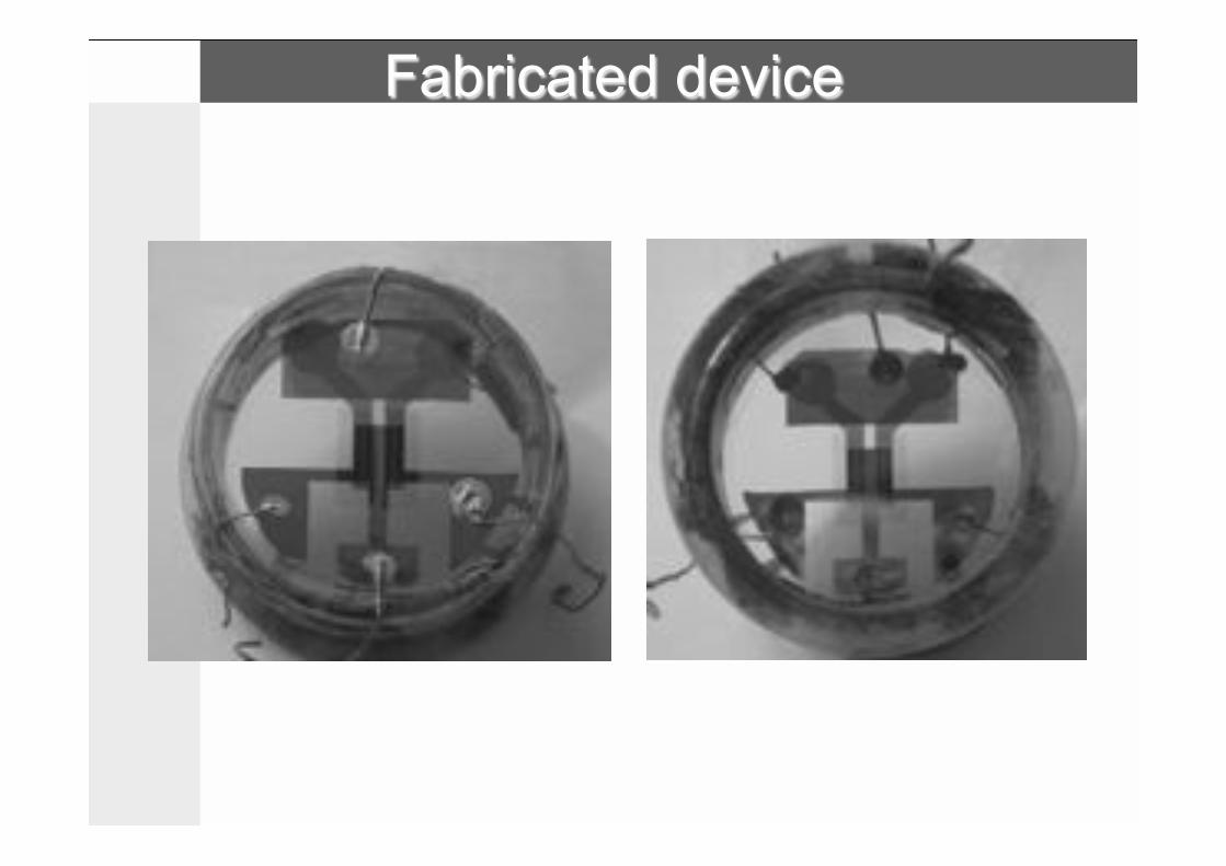
Fabricated device
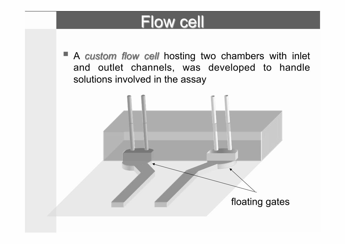
Flow cell
floating gates
# A custom flow cell hosting two chambers with inlet and outlet channels, was developed to handle solutions involved in the assay
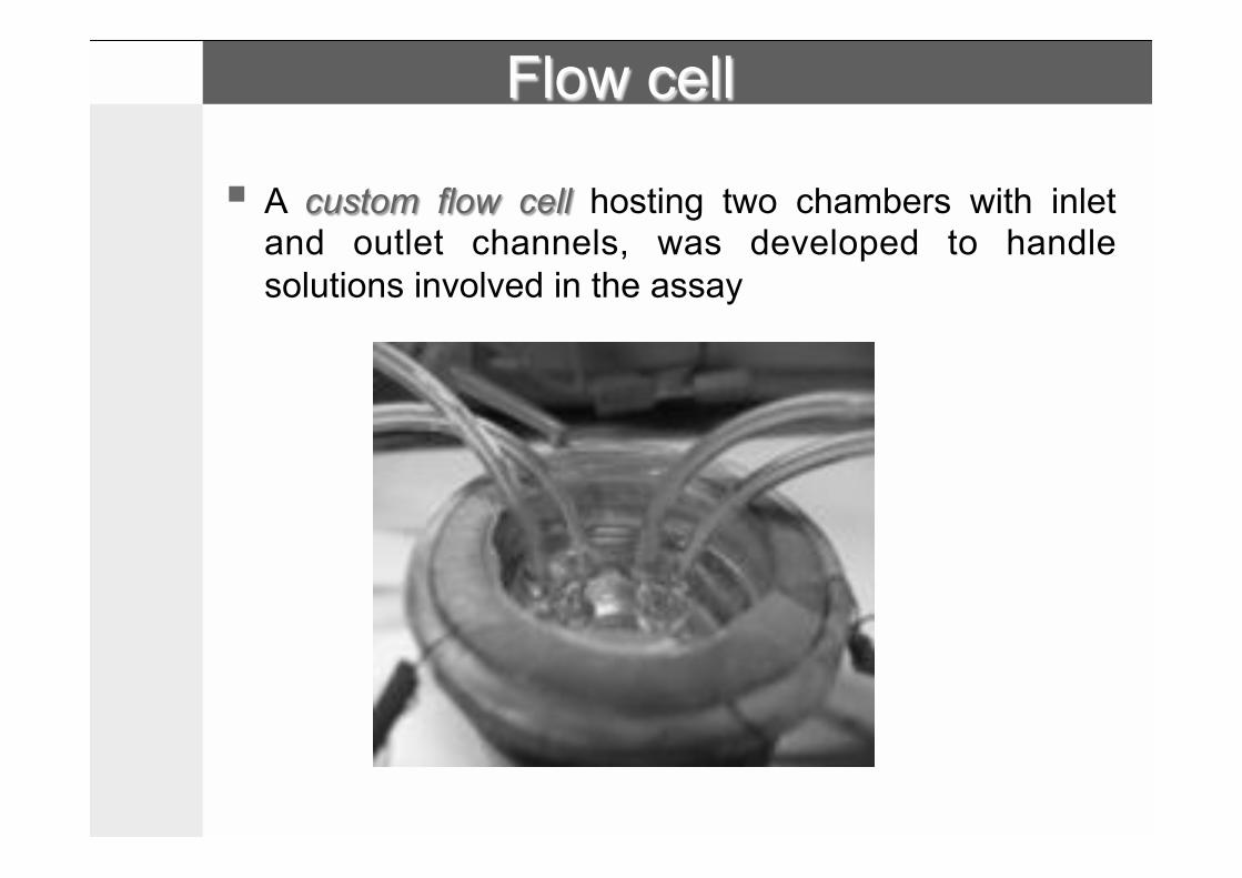
Flow cell
# A custom flow cell hosting two chambers with inlet and outlet channels, was developed to handle solutions involved in the assay
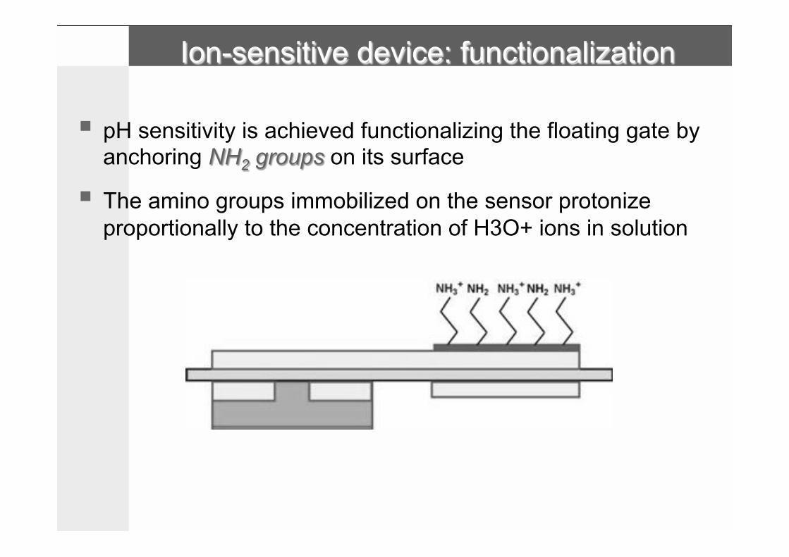
# pH sensitivity is achieved functionalizing the floating gate by anchoring NH2 groups on its surface
# The amino groups immobilized on the sensor protonize proportionally to the concentration of H3O+ ions in solution
Ion-sensitive device: functionalization
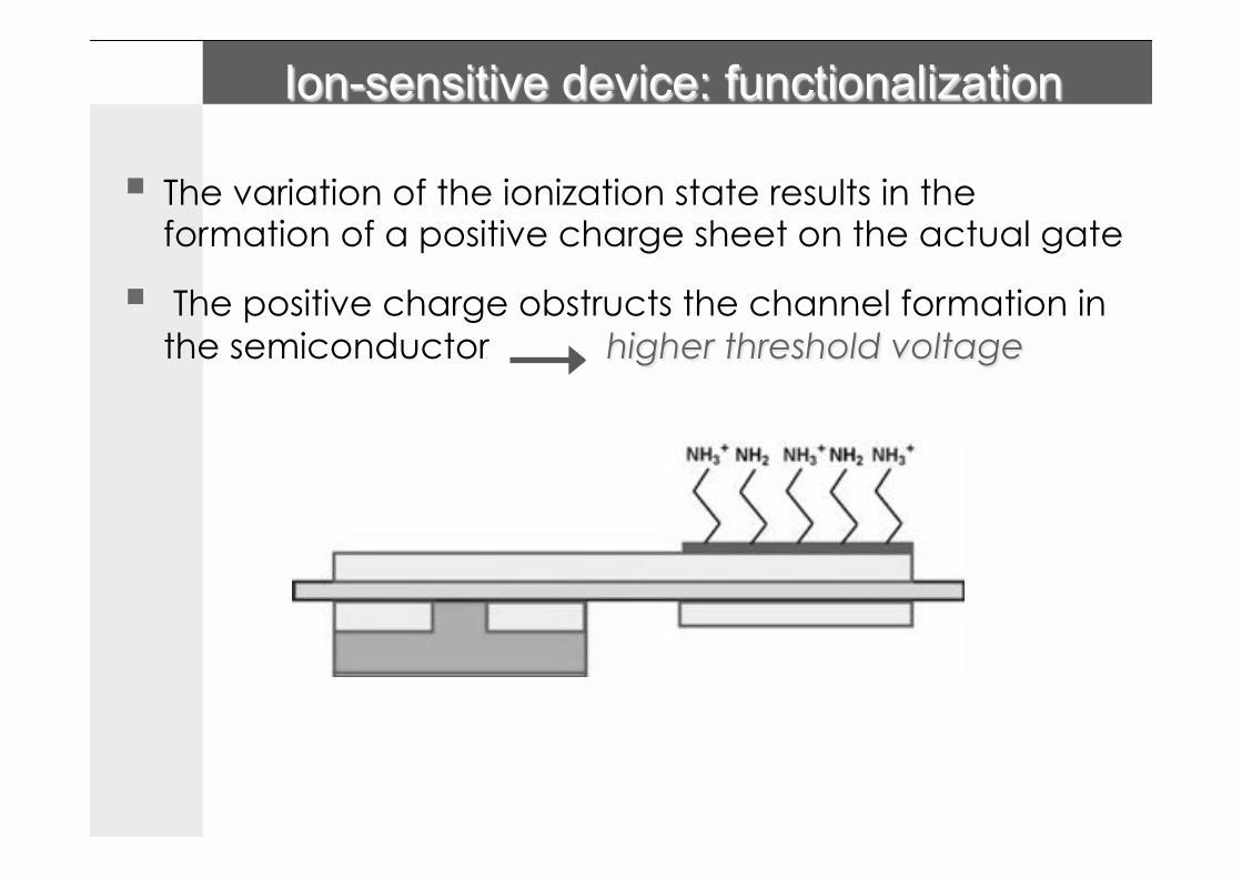
# The variation of the ionization state results in the formation of a positive charge sheet on the actual gate
# The positive charge obstructs the channel formation in the semiconductor higher threshold voltage
Ion-sensitive device: functionalization
Ion-sensitive device: functionalization
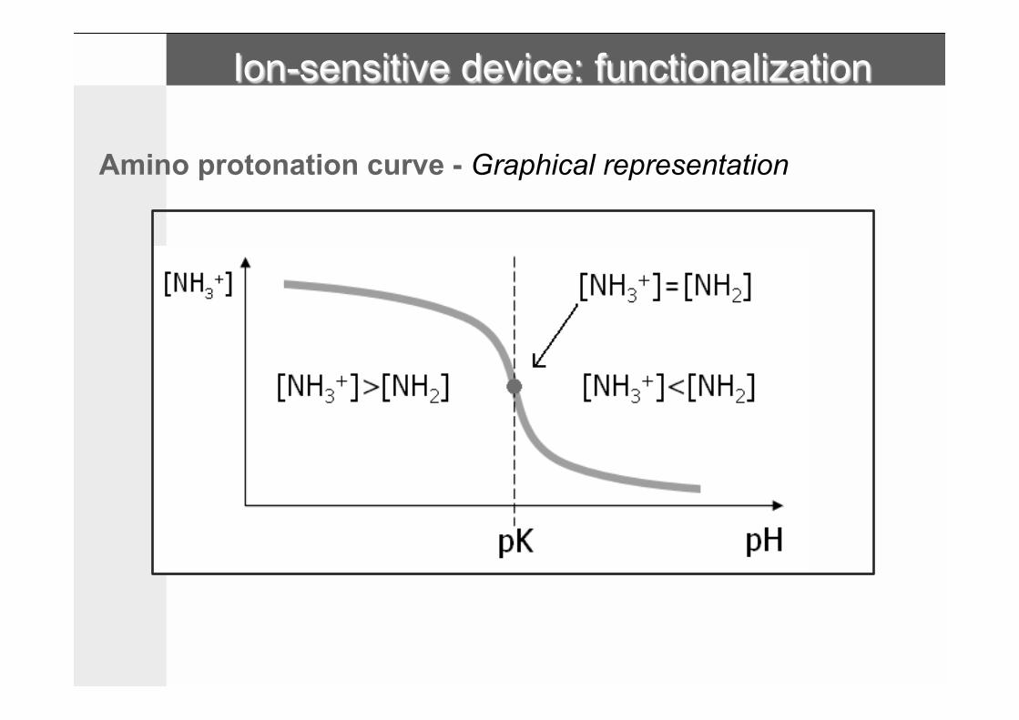
Amino protonation curve - Graphical representation
3 4 5 6 7 8
1000
1200
1400
1600
1800
2000Rct-[Ω
]
pH
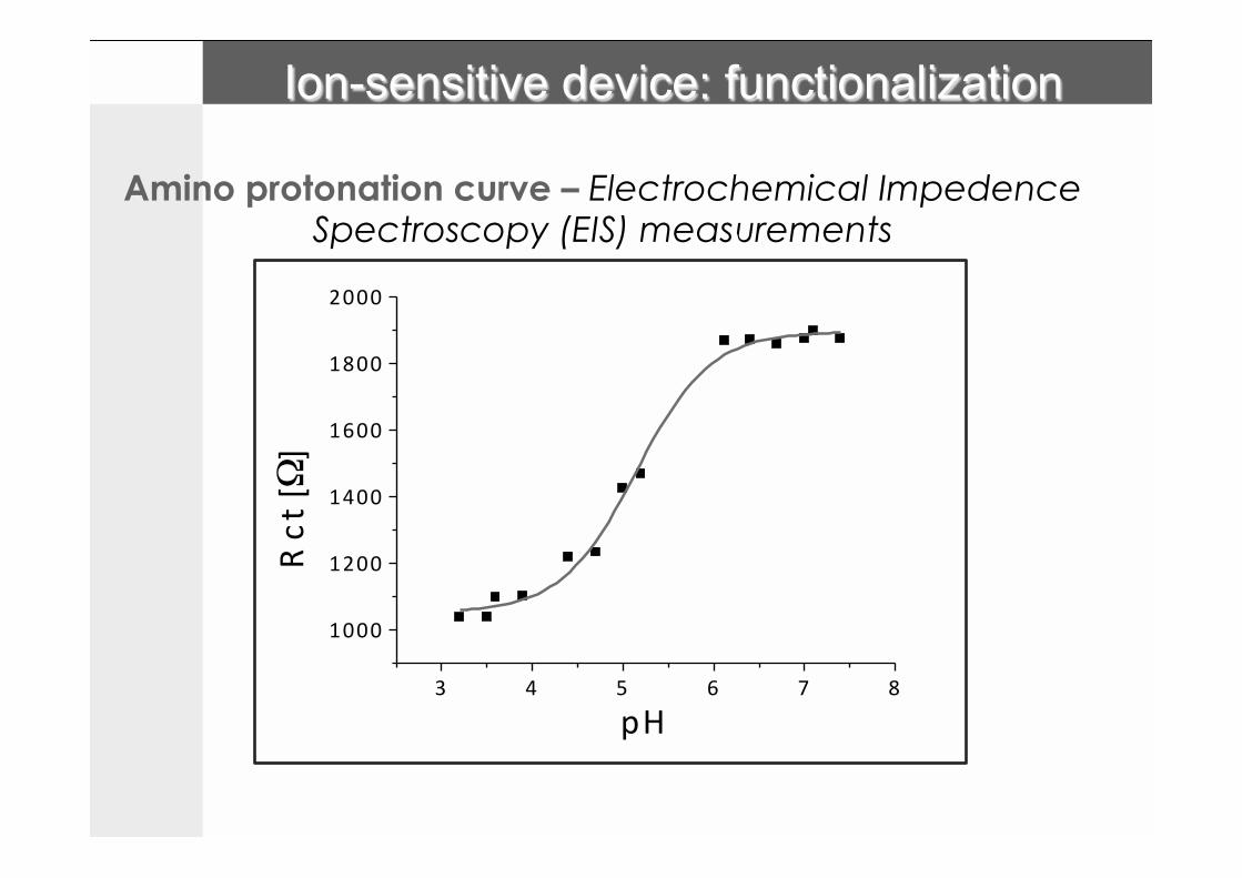
Amino protonation curve – Electrochemical Impedence Spectroscopy (EIS) measurements
Ion-sensitive device: functionalization
• The device has the typical behavior of an organic p-type field effect transistor, working in accumulation mode
• The ion-sensitivity was tested measuring the variation in the drain-source current induced by the change in the pH value of the solution
• The testing was carried out by replacing the solution under investigation by means of the custom-developed fluidic system
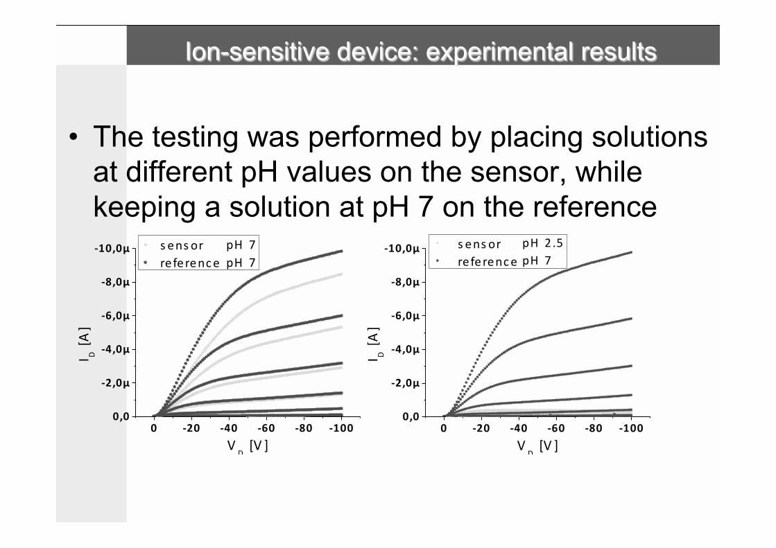
Ion-sensitive device: experimental results
0 "20 "40 "60 "80 "1000,0
"2,0µ
"4,0µ
"6,0µ
"8,0µ
"10,0µ s ens or&& & & & &re ference &&
I D&[A
]
VD&[V ]
pH &7pH &7
0 "20 "40 "60 "80 "1000,0
"2,0µ
"4,0µ
"6,0µ
"8,0µ
"10,0µ !s ens or!! ! ! ! !!re ference !!
I D![A
]
VD![V ]
pH !2 .5pH !7
• The testing was performed by placing solutions at different pH values on the sensor, while keeping a solution at pH 7 on the reference
Ion-sensitive device: experimental results
0 "20 "40 "60 "80 "1000,0
"800,0n
"1,6µ
"2,4µ
"3,2µ
"4,0µ
"4,8µs ens or&& &pH &2.5
I D&[A
]
VD&[V ]
0 "20 "40 "60 "80 "1000,0
"800,0n
"1,6µ
"2,4µ
"3,2µ
"4,0µ
"4,8µ
I D#[A
]V
D#[V ]
s ens or## #pH #3.5
0 "20 "40 "60 "80 "1000,0
"800,0n
"1,6µ
"2,4µ
"3,2µ
"4,0µ
"4,8µ
I D#[A
]
VD#[V ]
#s ens or## #pH #4
0 "20 "40 "60 "80 "1000,0
"800,0n
"1,6µ
"2,4µ
"3,2µ
"4,0µ
"4,8µ
I D#[A
]
VD#[V ]
#s ens or## #pH #5
0 "20 "40 "60 "80 "1000,0
"800,0n
"1,6µ
"2,4µ
"3,2µ
"4,0µ
"4,8µ
I D#[A
]
VD#[V ]
s ens or## #pH #6
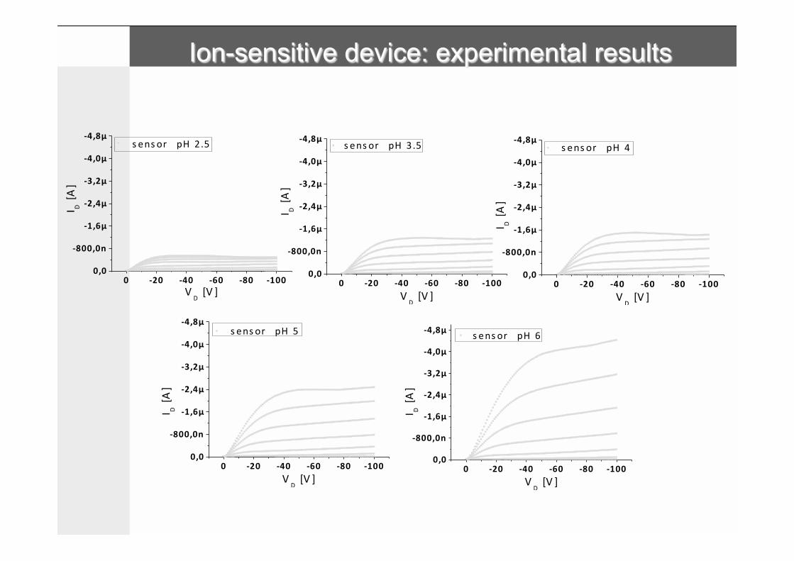
Ion-sensitive device: experimental results
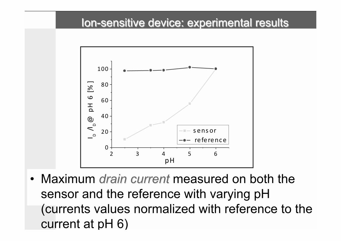
• Maximum drain current measured on both the sensor and the reference with varying pH (currents values normalized with reference to the current at pH 6)
2 3 4 5 60
20
40
60
80
100
))s ens or))re ferenceI D
)/ID@
)pH)6)[%
]
pH
Ion-sensitive device: experimental results
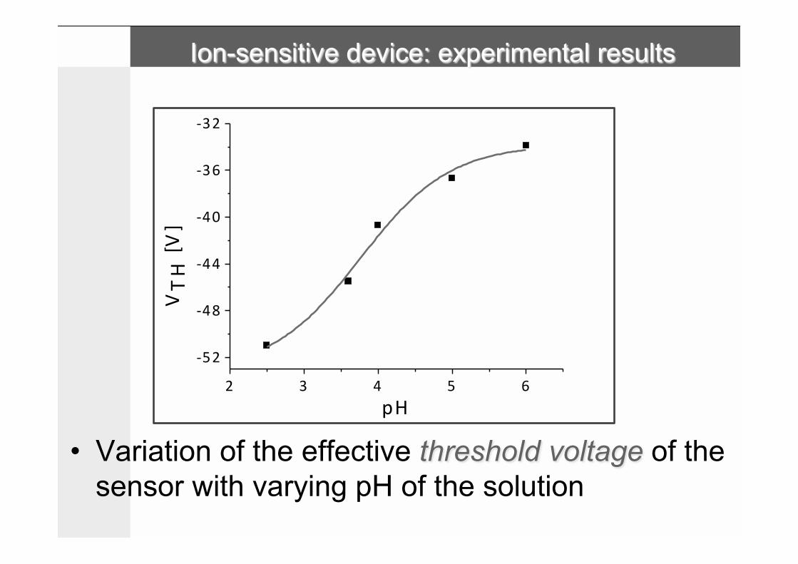
• Variation of the effective threshold voltage of the sensor with varying pH of the solution
2 3 4 5 6
&52
&48
&44
&40
&36
&32
VTH,[V
]
pH
amino groups protonation
3 4 5 6 7 8
1,0k
1,2k
1,4k
1,6k
1,8k
2,0k
Rct/[Ω
]
pH
Ion-sensitive device: experimental results
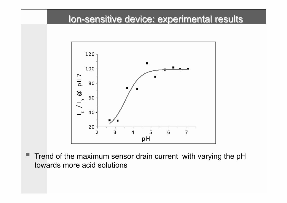
2 3 4 5 6 720
40
60
80
100
120
I D,/,I D,@
,pH7
pH
# Trend of the maximum sensor drain current with varying the pH towards more acid solutions
Ion-sensitive device: experimental results
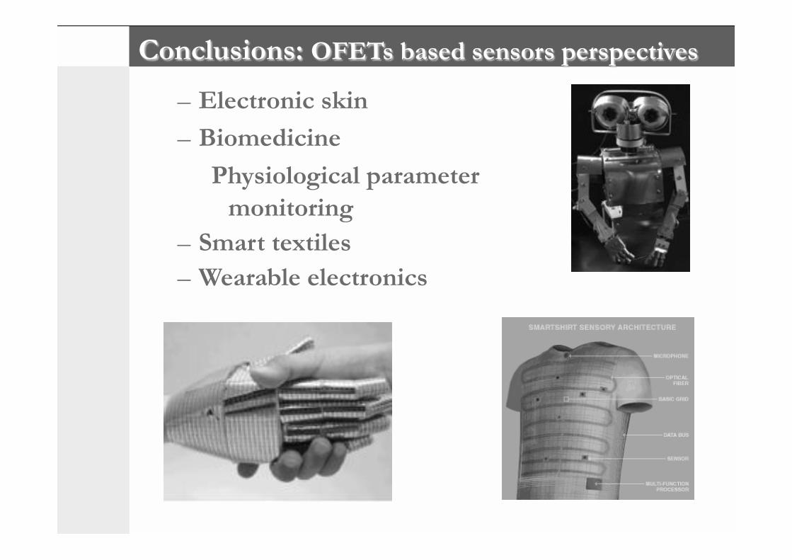
– Electronic skin – Biomedicine
Physiological parameter monitoring
– Smart textiles – Wearable electronics
Conclusions: OFETs based sensors perspectives
Recommended