A4(210 X 297)
PRODUCT GROUP
TFT-LCDP1
ISSUE DATE
2019/08/22
PAGE
DV550QUM-N10
Preliminary Product Specification
P1
A4(210 X 297)
PAGE
OF 40
PROPRIETARY NOTE
THIS SPECIFICATION IS THE PROPERTY OF BOE FZ AND SHALL NOT BE
REPRODUCED OR COPIED WITHOUT THE WRITTEN PERMISSION OF BOE FZ AND
MUST BE RETURNED TO BOE FZ UPON ITS REQUEST
DAS-RD-2019028-O
SPEC. NUMBER
S8-65-8D-080
FUZHOU BOE OPTOELECTRONICS TECHNOLOGY Co.,LTD
1
DAS-RD-2019028-O A4(210 X 297)
PAGE
OF 40
Revision No. Page Description of changes Date Prepared
P0 - Initial Release 2019/08/14 Tang Guichun
P1 11Update LED Light bar Unit
Characteristics 2019/08/22 Tang Guichun
REVISION HISTORY
PRODUCT GROUP REV ISSUE DATE
Customer SPEC
(√ )preliminary specification
( )Final specification
SPEC. NUMBER
S8-65-8D-080
P1 2019/08/22
SPEC. TITLE
DV550QUM-N10 Preliminary Product Specification P1 2
A4(210 X 297)
PAGE
REV ISSUE DATEPRODUCT GROUP
Customer SPEC
OF 40
SPEC. TITLE
DV550QUM-N10 Preliminary Product Specification P1
DAS-RD-2019028-O
SPEC. NUMBER
S8-65-8D-080
P1 2019/08/22
3
Contents
No. Item Page
1.0 GENERAL DESCRIPTION 4
2.0 ABSOLUTE MAXIMUM RATINGS 6
3.0 ELECTRICAL SPECIFICATIONS 7
4.0 INTERFACE CONNECTION 15
5.0 SIGNAL TIMING WAVEFORMS OF INTERFACE SIGNAL 23
6.0 SIGNAL TIMING SPECIFICATION 25
7.0 OPTICAL SPECIFICATION 28
8.0 MECHANICAL CHARACTERISTICS 31
9.0 RELIABILITY TEST 32
10.0 HANDLING & CAUTIONS 33
11.0 PRODUCT SERIAL NUMBER 34
12.0 PACKING 35
13.0 APPENDIX 37

A4(210 X 297)
PAGE
REV ISSUE DATEPRODUCT GROUP
Customer SPEC
OF 40
SPEC. TITLE
DV550QUM-N10 Preliminary Product Specification P1
DAS-RD-2019028-O
SPEC. NUMBER
S8-65-8D-080
P1 2019/08/22
4
1.0 GENERAL DESCRIPTION
DV550QUM-N10 is a color active matrix TFT LCD module using amorphous silicon TFT's
(Thin Film Transistors) as an active switching device. This module has a 54.64 inch
diagonally measured active area with UHD resolutions (3840 horizontal by 2160 vertical
pixel array). Each pixel is divided into RED, GREEN, BLUE dots which are arranged in
island and this module can display 1.07G colors. The TFT-LCD panel used for this module
is adapted for a low reflection and higher color type.
1.1 Introduction
1.2 Features
V by one interface with 8 lanes
High-speed response
Low color shift image quality
8-bit + FRC color depth, display 1.07G colors
High luminance and contrast ratio, low reflection and wide viewing angle
DE (Data Enable) only mode
ADS technology is applied for high display quality
RoHS compliant
Horizontal and Perpendicular compatibility(Vertical Spec:Rotate 90°clockwise facing
the LCM front)
Source Driver
TFT - LCD Panel(3840 × RGB × 2160 pixels)
G1
G2160
RGB(CEDS)
Timing Controller
[V by one Rx & CEDS
Tx integrated]
GO
A
Power Circuit
Block
+12.0V
VDD
CN1
(51pin)
8 lanes
V by one
LOCKN
HTPDN
S5761 S1

A4(210 X 297)
PAGE
REV ISSUE DATEPRODUCT GROUP
Customer SPEC
OF 40
SPEC. TITLE
DV550QUM-N10 Preliminary Product Specification P1
DAS-RD-2019028-O
SPEC. NUMBER
S8-65-8D-080
P1 2019/08/22
Parameter Specification Unit Remark
Active area 1209.6(H) × 680.4(V) mm
Number of pixels 3840*(RGB)*2160 pixels
Pixel pitch 315(H) ×315(V) μm
Pixel arrangement Pixels RGB Island
Display colors 1.07G (8bits + FRC ) colors
Luminance, White Min720, Typ. 800 nit
Viewing Angle (CR>10)
Viewing angle free ( R/L 178 (Typ.), U/D 178 (Typ.))
Display mode Transmission mode, Normally Black
Open Cell Transmittance
5.4 %At center point with BOE BLU
Weight 15 Kg Module
Power ConsumptionTotal: Typ:120.86 Max:153.51Logic: Typ:12 Max:36BLU: Typ:108.86 Max:117.51
Watt
Surface TreatmentHaze 1% , 3H, Anti-Glare Layer
(for Front and Rear Polarizer)
RemarkHorizontal and Perpendicular compatibility(Vertical Spec:Rotate
90° clockwise facing the LCM front)
< Table 1. General Specifications >
1.3 Application
Home Alone Multimedia TFT-LCD TV
Display Terminals for Control System
Ultra High Definition TV(UHD TV)
AV application Products
1.4 General Specification
1.0 GENERAL DESCRIPTION
5
A4(210 X 297)
PAGE
REV ISSUE DATEPRODUCT GROUP
Customer SPEC
OF 40
SPEC. TITLE
DV550QUM-N10 Preliminary Product Specification P1
DAS-RD-2019028-O
SPEC. NUMBER
S8-65-8D-080
P1 2019/08/22
6
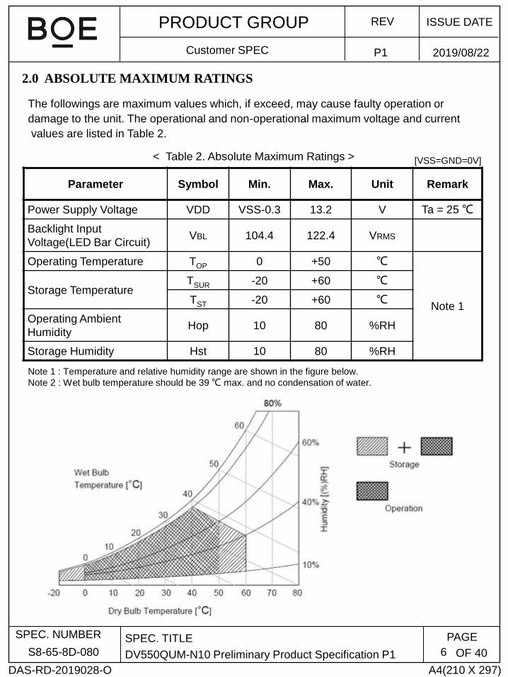
2.0 ABSOLUTE MAXIMUM RATINGS
The followings are maximum values which, if exceed, may cause faulty operation or
damage to the unit. The operational and non-operational maximum voltage and current
values are listed in Table 2.
Parameter Symbol Min. Max. Unit Remark
Power Supply Voltage VDD VSS-0.3 13.2 V Ta = 25 ℃
Backlight Input
Voltage(LED Bar Circuit)VBL 104.4 122.4 VRMS
Operating Temperature TOP 0 +50 ℃
Note 1
Storage TemperatureTSUR -20 +60 ℃
TST -20 +60 ℃
Operating Ambient
HumidityHop 10 80 %RH
Storage Humidity Hst 10 80 %RH
< Table 2. Absolute Maximum Ratings > [VSS=GND=0V]
Note 1 : Temperature and relative humidity range are shown in the figure below.
Note 2 : Wet bulb temperature should be 39 ℃ max. and no condensation of water.
A4(210 X 297)
PAGE
REV ISSUE DATEPRODUCT GROUP
Customer SPEC
OF 40
SPEC. TITLE
DV550QUM-N10 Preliminary Product Specification P1
DAS-RD-2019028-O
SPEC. NUMBER
S8-65-8D-080
P1 2019/08/22
7
Note 1 : The supply voltage is measured and specified at the interface connector of LCM.
The current draw and power consumption specified is for VDD=12.0V.
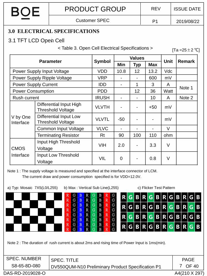
a) Typ: Mosaic 7X5(L0/L255) b) Max : Vertical Sub Line(L255) c) Flicker Test Pattern
Note 2 : The duration of rush current is about 2ms and rising time of Power Input is 1ms(min).
3.0 ELECTRICAL SPECIFICATIONS
[Ta =25± 2 ℃]< Table 3. Open Cell Electrical Specifications >
3.1 TFT LCD Open Cell
Parameter SymbolValues
Unit RemarkMin Typ Max
Power Supply Input Voltage VDD 10.8 12 13.2 Vdc
Power Supply Ripple Voltage VRP - - 600 mV
Power Supply Current IDD - 1 3 ANote 1
Power Consumption PDD 12 36 Watt
Rush current IRUSH - - 10 A Note 2
V by One
Interface
Differential Input High
Threshold VoltageVLVTH - - +50 mV
Differential Input Low
Threshold VoltageVLVTL -50 - - mV
Common Input Voltage VLVC - - - V
Terminating Resistor Rt 90 100 110 ohm
CMOS
Interface
Input High Threshold
VoltageVIH 2.0 - 3.3 V
Input Low Threshold
VoltageVIL 0 - 0.8 V
R G B R G B R G
R G B R G B R G
R G B R G B R G
R G B R G B R G
R G B R G B R G
R G B R G B R G
R G B R G B R G
R G B R G B R G
R G B R G B R G B R G B
R G B R G B R G B R G B
R G B R G B R G B R G B
R G B R G B R G B R G B
A4(210 X 297)
PAGE
REV ISSUE DATEPRODUCT GROUP
Customer SPEC
OF 40
SPEC. TITLE
DV550QUM-N10 Preliminary Product Specification P1
DAS-RD-2019028-O
SPEC. NUMBER
S8-65-8D-080
P1 2019/08/22
8
< Table 4. TCON Characteristics >
Note 1 : Any point on the TCON surface must be less than 110 ℃ under any conditions.
3.2 IC Characteristics
Parameter SymbolValues
Unit RemarkMin Typ Max
TCON Surface Temperature TTS - - 110 ℃ Note
< Table 5. Driver Characteristics >
Note 3 : Any point on the driver surface must be less than 125 ℃ under any conditions.
Parameter SymbolValues
Unit RemarkMin Typ Max
Driver Surface Temperature TDS - - 125 ℃ Note
Note 2 : This test condition is based on BOE module.
Note 4: This test condition is based on BOE module.
< Table 6. PMIC Characteristics >
Note 5 : Any point on the PMIC surface must be less than 100 ℃ under any conditions.
Parameter SymbolValues
Unit RemarkMin Typ Max
PMIC Surface Temperature TPS - - 100 ℃ Note
Note 6: This test condition is based on BOE module.
3.0 ELECTRICAL SPECIFICATIONS
A4(210 X 297)
PAGE
REV ISSUE DATEPRODUCT GROUP
Customer SPEC
OF 40
SPEC. TITLE
DV550QUM-N10 Preliminary Product Specification P1
DAS-RD-2019028-O
SPEC. NUMBER
S8-65-8D-080
P1 2019/08/22
9
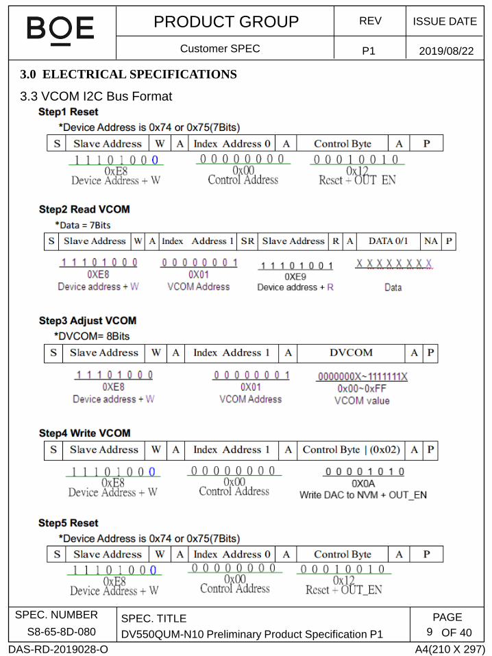
3.3 VCOM I2C Bus Format
3.0 ELECTRICAL SPECIFICATIONS

A4(210 X 297)
PAGE
REV ISSUE DATEPRODUCT GROUP
Customer SPEC
OF 40
SPEC. TITLE
DV550QUM-N10 Preliminary Product Specification P1
DAS-RD-2019028-O
SPEC. NUMBER
S8-65-8D-080
P1 2019/08/22
10
3.0 ELECTRICAL SPECIFICATIONS
3.4 Interval of step to step

A4(210 X 297)
PAGE
REV ISSUE DATEPRODUCT GROUP
Customer SPEC
OF 40
SPEC. TITLE
DV550QUM-N10 Preliminary Product Specification P1
DAS-RD-2019028-O
SPEC. NUMBER
S8-65-8D-080
P1 2019/08/22
11
3.0 ELECTRICAL SPECIFICATIONS
[Ta =25± 2 ℃]
3.5 Backlight Module
< Table 7. LED LIGHTBAR UNIT CHARACTERISTICS >
Parameter Symbol Min. Typ. Max. Unit Remarks
LED Forward Voltage V 104.4 113.4 122.4 V -
LED Forward Current I - 880 mA -
LED Power Consumption W 91.9 99.8 107.8 W -
LED Life-Time L 50,000 - - Hour Note 1
Note1 :The lifetime is defined as the time which luminance of the LED decays to 50%
compared to the initial value, Operating condition: Continuous operating at Ta = 25± 2℃
-LED Bar Block Diagram
LED Numbers: 2bar / BLU
Total: 144LED / BLU
A4(210 X 297)
PAGE
REV ISSUE DATEPRODUCT GROUP
Customer SPEC
OF 40
SPEC. TITLE
DV550QUM-N10 Preliminary Product Specification P1
DAS-RD-2019028-O
SPEC. NUMBER
S8-65-8D-080
P1 2019/08/22
12
3.0 ELECTRICAL SPECIFICATIONS
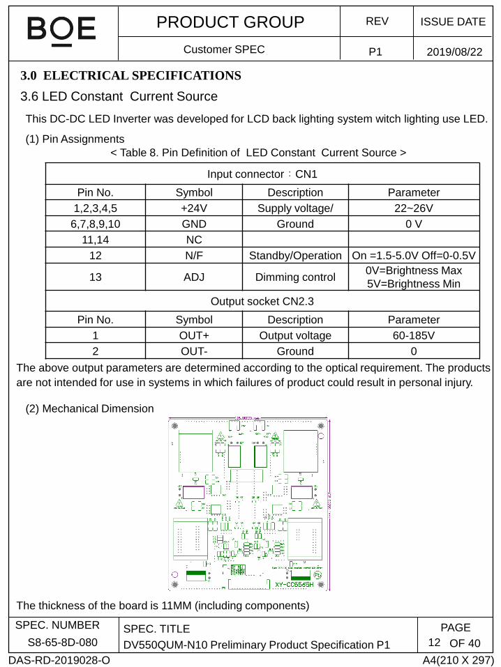
3.6 LED Constant Current Source
This DC-DC LED Inverter was developed for LCD back lighting system witch lighting use LED.
(1) Pin Assignments
Input connector:CN1
Pin No. Symbol Description Parameter
1,2,3,4,5 +24V Supply voltage/ 22~26V
6,7,8,9,10 GND Ground 0 V
11,14 NC
12 N/F Standby/Operation On =1.5-5.0V Off=0-0.5V
13 ADJ Dimming control0V=Brightness Max
5V=Brightness Min
Output socket CN2.3
Pin No. Symbol Description Parameter
1 OUT+ Output voltage 60-185V
2 OUT- Ground 0
(2) Mechanical Dimension
< Table 8. Pin Definition of LED Constant Current Source >
The above output parameters are determined according to the optical requirement. The products
are not intended for use in systems in which failures of product could result in personal injury.
The thickness of the board is 11MM (including components)

A4(210 X 297)
PAGE
REV ISSUE DATEPRODUCT GROUP
Customer SPEC
OF 40
SPEC. TITLE
DV550QUM-N10 Preliminary Product Specification P1
DAS-RD-2019028-O
SPEC. NUMBER
S8-65-8D-080
P1 2019/08/22
13
(4) Electrical Characteristics
NO Item Symbol Test Conditions Min Type Max Unit
1 Input Voltage Vin 22 24 26 V
2 Input Current Iin 4.75 6 A
3 Input Power Pin 104 142 W
4 Brightness Voltage Vadj 0(Bright) - 5(Dark) V
5 Control Voltage Enable Von=1.5~5.0V Disable Voff=0~0.5V
6Output Current (per g
roup)Iout
Vin=24.0V; Vout=57V; Ta
=28℃440 600 mA
7 Output Voltage Vout Vin=24.0V; Ta=28℃ 60 118.8 185 V
8 Efficiency η Vin=24.0V; Vout=118V; 92.5 %
9 Output Total Group Ggp 2
10 Total Output Current R 880 1200 mA
11 Output Power Wout Vin=24.0V; Vout=122.4V; 104 142 W
3.6 LED Constant Current Source
3.0 ELECTRICAL SPECIFICATIONS
Operating temperature Storage temperature Operating humidity Storage humidity Remark
-50℃ -- 65℃ -20℃-- 70℃ 10% -- 95%RH 10% -- 95%RH Note1
-20℃ -- 70℃ 10% -- 95%RH Note2
(3) Environmental Condition
Note1: The DC to DC back-light inverter suggested working in the condition.
Note2: It can be work 300 thousand hours at least in the condition.
< Table 9. LED Constant Current Source Working Condition >
< Table 10. LED Constant Current Source Electrical Characteristics >
A4(210 X 297)
PAGE
REV ISSUE DATEPRODUCT GROUP
Customer SPEC
OF 40
SPEC. TITLE
DV550QUM-N10 Preliminary Product Specification P1
DAS-RD-2019028-O
SPEC. NUMBER
S8-65-8D-080
P1 2019/08/22
14
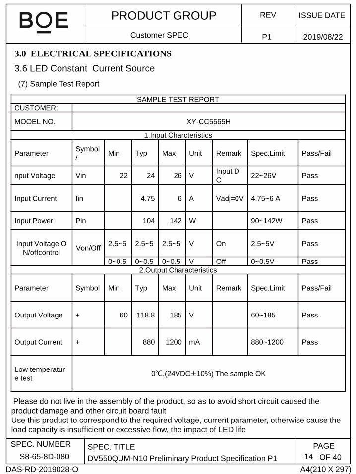
SAMPLE TEST REPORT
CUSTOMER:
MOOEL NO. XY-CC5565H
1.Input Charcteristics
ParameterSymbol
/Min Typ Max Unit Remark Spec.Limit Pass/Fail
nput Voltage Vin 22 24 26 VInput D
C22~26V Pass
Input Current Iin 4.75 6 A Vadj=0V 4.75~6 A Pass
Input Power Pin 104 142 W 90~142W Pass
Input Voltage O
N/offcontrolVon/Off
2.5~5 2.5~5 2.5~5 V On 2.5~5V Pass
0~0.5 0~0.5 0~0.5 V Off 0~0.5V Pass
2.Output Characteristics
Parameter Symbol Min Typ Max Unit Remark Spec.Limit Pass/Fail
Output Voltage + 60 118.8 185 V 60~185 Pass
Output Current + 880 1200 mA 880~1200 Pass
Low temperatur
e test0℃,(24VDC± 10%) The sample OK
Please do not live in the assembly of the product, so as to avoid short circuit caused the
product damage and other circuit board fault
Use this product to correspond to the required voltage, current parameter, otherwise cause the
load capacity is insufficient or excessive flow, the impact of LED life
3.6 LED Constant Current Source
3.0 ELECTRICAL SPECIFICATIONS
(7) Sample Test Report
A4(210 X 297)
PAGE
REV ISSUE DATEPRODUCT GROUP
Customer SPEC
OF 40
SPEC. TITLE
DV550QUM-N10 Preliminary Product Specification P1
DAS-RD-2019028-O
SPEC. NUMBER
S8-65-8D-080
P1 2019/08/22
15
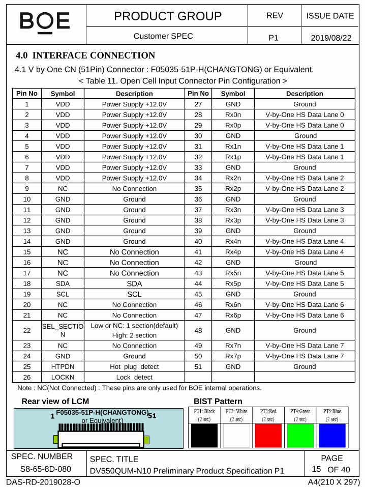
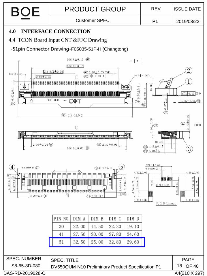
4.0 INTERFACE CONNECTION
4.1 V by One CN (51Pin) Connector : F05035-51P-H(CHANGTONG) or Equivalent.
< Table 11. Open Cell Input Connector Pin Configuration >
Pin No Symbol Description Pin No Symbol Description
1 VDD Power Supply +12.0V 27 GND Ground
2 VDD Power Supply +12.0V 28 Rx0n V-by-One HS Data Lane 0
3 VDD Power Supply +12.0V 29 Rx0p V-by-One HS Data Lane 0
4 VDD Power Supply +12.0V 30 GND Ground
5 VDD Power Supply +12.0V 31 Rx1n V-by-One HS Data Lane 1
6 VDD Power Supply +12.0V 32 Rx1p V-by-One HS Data Lane 1
7 VDD Power Supply +12.0V 33 GND Ground
8 VDD Power Supply +12.0V 34 Rx2n V-by-One HS Data Lane 2
9 NC No Connection 35 Rx2p V-by-One HS Data Lane 2
10 GND Ground 36 GND Ground
11 GND Ground 37 Rx3n V-by-One HS Data Lane 3
12 GND Ground 38 Rx3p V-by-One HS Data Lane 3
13 GND Ground 39 GND Ground
14 GND Ground 40 Rx4n V-by-One HS Data Lane 4
15 NC No Connection 41 Rx4p V-by-One HS Data Lane 4
16 NC No Connection 42 GND Ground
17 NC No Connection 43 Rx5n V-by-One HS Data Lane 5
18 SDA SDA 44 Rx5p V-by-One HS Data Lane 5
19 SCL SCL 45 GND Ground
20 NC No Connection 46 Rx6n V-by-One HS Data Lane 6
21 NC No Connection 47 Rx6p V-by-One HS Data Lane 6
22SEL_SECTIO
N
Low or NC: 1 section(default)
High: 2 section48 GND Ground
23 NC No Connection 49 Rx7n V-by-One HS Data Lane 7
24 GND Ground 50 Rx7p V-by-One HS Data Lane 7
25 HTPDN Hot plug detect 51 GND Ground
26 LOCKN Lock detect
Note : NC(Not Connected) : These pins are only used for BOE internal operations.
511
Rear view of LCM
F05035-51P-H(CHANGTONG)
or Equivalent)
BIST Pattern
A4(210 X 297)
PAGE
REV ISSUE DATEPRODUCT GROUP
Customer SPEC
OF 40
SPEC. TITLE
DV550QUM-N10 Preliminary Product Specification P1
DAS-RD-2019028-O
SPEC. NUMBER
S8-65-8D-080
P1 2019/08/22
16
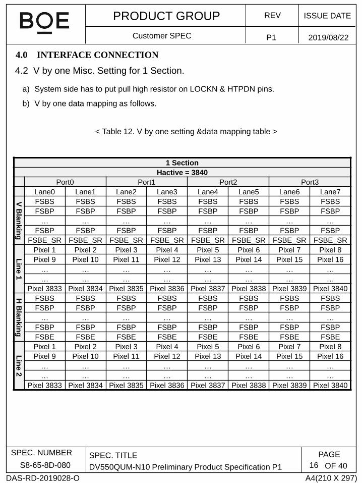
4.2 V by one Misc. Setting for 1 Section.
a) System side has to put pull high resistor on LOCKN & HTPDN pins.
b) V by one data mapping as follows.
< Table 12. V by one setting &data mapping table >
1 Section
Hactive = 3840
Port0 Port1 Port2 Port3
Lane0 Lane1 Lane2 Lane3 Lane4 Lane5 Lane6 Lane7
V B
lan
kin
g
FSBS FSBS FSBS FSBS FSBS FSBS FSBS FSBS
FSBP FSBP FSBP FSBP FSBP FSBP FSBP FSBP
… … … … … … … …
FSBP FSBP FSBP FSBP FSBP FSBP FSBP FSBP
FSBE_SR FSBE_SR FSBE_SR FSBE_SR FSBE_SR FSBE_SR FSBE_SR FSBE_SR
Lin
e 1
Pixel 1 Pixel 2 Pixel 3 Pixel 4 Pixel 5 Pixel 6 Pixel 7 Pixel 8
Pixel 9 Pixel 10 Pixel 11 Pixel 12 Pixel 13 Pixel 14 Pixel 15 Pixel 16
… … … … … … … …
… … … … … … … …
Pixel 3833 Pixel 3834 Pixel 3835 Pixel 3836 Pixel 3837 Pixel 3838 Pixel 3839 Pixel 3840
H B
lan
kin
g
FSBS FSBS FSBS FSBS FSBS FSBS FSBS FSBS
FSBP FSBP FSBP FSBP FSBP FSBP FSBP FSBP
… … … … … … … …
FSBP FSBP FSBP FSBP FSBP FSBP FSBP FSBP
FSBE FSBE FSBE FSBE FSBE FSBE FSBE FSBEL
ine
2Pixel 1 Pixel 2 Pixel 3 Pixel 4 Pixel 5 Pixel 6 Pixel 7 Pixel 8
Pixel 9 Pixel 10 Pixel 11 Pixel 12 Pixel 13 Pixel 14 Pixel 15 Pixel 16
… … … … … … … …
… … … … … … … …
Pixel 3833 Pixel 3834 Pixel 3835 Pixel 3836 Pixel 3837 Pixel 3838 Pixel 3839 Pixel 3840
4.0 INTERFACE CONNECTION

A4(210 X 297)
PAGE
REV ISSUE DATEPRODUCT GROUP
Customer SPEC
OF 40
SPEC. TITLE
DV550QUM-N10 Preliminary Product Specification P1
DAS-RD-2019028-O
SPEC. NUMBER
S8-65-8D-080
P1 2019/08/22
17
4.3 V by one Misc. Setting for 2 Section.
a) System side has to put pull high resistor on LOCKN & HTPDN pins.
b) V by one data mapping as follows.
< Table 13. V by one setting &data mapping table >
2 Section
Hactive = 3840
Port0 Port1 Port2 Port3
Lane0 Lane1 Lane2 Lane3 Lane4 Lane5 Lane6 Lane7
V B
lan
kin
g
FSBS FSBS FSBS FSBS FSBS FSBS FSBS FSBS
FSBP FSBP FSBP FSBP FSBP FSBP FSBP FSBP
… … … … … … … …
FSBP FSBP FSBP FSBP FSBP FSBP FSBP FSBP
FSBE_SR FSBE_SR FSBE_SR FSBE_SR FSBE_SR FSBE_SR FSBE_SR FSBE_SR
Lin
e 1
Pixel 1 Pixel 2 Pixel 3 Pixel 4 Pixel 1921 Pixel 1922 Pixel 1923 Pixel 1924
Pixel 5 Pixel 6 Pixel 7 Pixel 8 Pixel 1925 Pixel 1926 Pixel 1927 Pixel 1928
… … … … … … … …
… … … … … … … …
Pixel 1917 Pixel 1918 Pixel 1919 Pixel 1920 Pixel 3837 Pixel 3838 Pixel 3839 Pixel 3840
H B
lan
kin
g
FSBS FSBS FSBS FSBS FSBS FSBS FSBS FSBS
FSBP FSBP FSBP FSBP FSBP FSBP FSBP FSBP
… … … … … … … …
FSBP FSBP FSBP FSBP FSBP FSBP FSBP FSBP
FSBE FSBE FSBE FSBE FSBE FSBE FSBE FSBEL
ine
2Pixel 1 Pixel 2 Pixel 3 Pixel 4 Pixel 1921 Pixel 1922 Pixel 1923 Pixel 1924
Pixel 5 Pixel 6 Pixel 7 Pixel 8 Pixel 1925 Pixel 1926 Pixel 1927 Pixel 1928
… … … … … … … …
… … … … … … … …
Pixel 1917 Pixel 1918 Pixel 1919 Pixel 1920 Pixel 3837 Pixel 3838 Pixel 3839 Pixel 3840
4.0 INTERFACE CONNECTION
A4(210 X 297)
PAGE
REV ISSUE DATEPRODUCT GROUP
Customer SPEC
OF 40
SPEC. TITLE
DV550QUM-N10 Preliminary Product Specification P1
DAS-RD-2019028-O
SPEC. NUMBER
S8-65-8D-080
P1 2019/08/22
18
4.4 TCON Board Input CNT &FFC Drawing
-51pin Connector Drawing-F05035-51P-H (Changtong)
4.0 INTERFACE CONNECTION

A4(210 X 297)
PAGE
REV ISSUE DATEPRODUCT GROUP
Customer SPEC
OF 40
SPEC. TITLE
DV550QUM-N10 Preliminary Product Specification P1
DAS-RD-2019028-O
SPEC. NUMBER
S8-65-8D-080
P1 2019/08/22
19
-51pin Connector Drawing-PM.FPC.LVS0505101(UJC)

A4(210 X 297)
PAGE
REV ISSUE DATEPRODUCT GROUP
Customer SPEC
OF 40
SPEC. TITLE
DV550QUM-N10 Preliminary Product Specification P1
DAS-RD-2019028-O
SPEC. NUMBER
S8-65-8D-080
P1 2019/08/22
20
-FFC Drawing
4.4 TCON Board Input CNT &FFC Drawing
4.0 INTERFACE CONNECTION
Note: It is BOE FFC drawing. Please refer to only one side for T-con Board.
100.00mm±0.5
30.00±
0.05
金手指面
29.55±
0.03
25.00±
0.05
2.275±
0.04
0.32±0.03
3.00±0.05
4.60±0.10
R0.60
0.50±0.03
两端裁切一样
R0.60
0.775+0.05
-0.020.775+0.05
-0.02
2.30±0.5 2.30±0.5
2.265±
0.04
0.3+0.03
-0.00
8.00(蓝色补强板)0.15 0.3+0.03
-0.00
8.00(蓝色补强板)
2.30±0.32.30Min
蓝色补强板侧

A4(210 X 297)
PAGE
REV ISSUE DATEPRODUCT GROUP
Customer SPEC
OF 40
SPEC. TITLE
DV550QUM-N10 Preliminary Product Specification P1
DAS-RD-2019028-O
SPEC. NUMBER
S8-65-8D-080
P1 2019/08/22
21
4.5 TCON Board Output CNT &FFC Drawing
-60pin Connector Drawing-PM.FPC.LVS0506001(UJC)
Note: TCON Board output CNT = XPCBA Input CNT.
4.0 INTERFACE CONNECTION

A4(210 X 297)
PAGE
REV ISSUE DATEPRODUCT GROUP
Customer SPEC
OF 40
SPEC. TITLE
DV550QUM-N10 Preliminary Product Specification P1
DAS-RD-2019028-O
SPEC. NUMBER
S8-65-8D-080
P1 2019/08/22
22
-60pin Connector Drawing-F05039-60P-H(Changtong)
-FFC Drawing
Note: TCON Board output CNT = XPCBA Input CNT.
Notes: This FFC drawing is supplied by the connector vendor.

A4(210 X 297)
PAGE
REV ISSUE DATEPRODUCT GROUP
Customer SPEC
OF 40
SPEC. TITLE
DV550QUM-N10 Preliminary Product Specification P1
DAS-RD-2019028-O
SPEC. NUMBER
S8-65-8D-080
P1 2019/08/22
23
5.1 Input data specification
<Table 14. Vx1 Byte length and Color mapping>
5.0 SIGNAL TIMING WAVEFORMS OF INTERFACE SIGNAL
Byte Packer inputColor data mapping
30 bpp RGB 24 bpp RGB
0
Bit-0 R2 R0
Bit-1 R3 R1
Bit-2 R4 R2
Bit-3 R5 R3
Bit-4 R6 R4
Bit-5 R7 R5
Bit-6 R8 R6
Bit-7 R9 R7
1
Bit-8 G2 G0
Bit-9 G3 G1
Bit-10 G4 G2
Bit-11 G5 G3
Bit-12 G6 G4
Bit-13 G7 G5
Bit-14 G8 G6
Bit-15 G9 G7
2
Bit-16 B2 B0
Bit-17 B3 B1
Bit-18 B4 B2
Bit-19 B5 B3
Bit-20 B6 B4
Bit-21 B7 B5
Bit-22 B8 B6
Bit-23 B9 B7
3
Bit-24 - -
Bit-25 - -
Bit-26 B0 -
Bit-27 B1 -
Bit-28 G0 -
Bit-29 G1 -
Bit-30 R0 -
Bit-31 R1 -
A4(210 X 297)
PAGE
REV ISSUE DATEPRODUCT GROUP
Customer SPEC
OF 40
SPEC. TITLE
DV550QUM-N10 Preliminary Product Specification P1
DAS-RD-2019028-O
SPEC. NUMBER
S8-65-8D-080
P1 2019/08/22
24
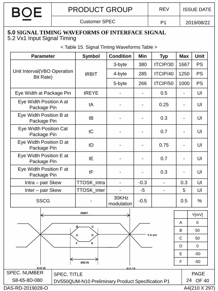
Parameter Symbol Condition Min Typ Max Unit
Unit Interval(VBO Operation
Bit Rate)tRBIT
3-byte 380 tTCIP/30 1667 PS
4-byte 285 tTCIP/40 1250 PS
5-byte 266 tTCIP/50 1000 PS
Eye Width at Package Pin tREYE - - 0.5 - UI
Eye Width Position A at
Package PintA - - 0.25 - UI
Eye Width Position B at
Package PintB - - 0.3 - UI
Eye Width Position Cat
Package PintC - - 0.7 - UI
Eye Width Position D at
Package PintD - - 0.75 - UI
Eye Width Position E at
Package PintE - - 0.7 - UI
Eye Width Position F at
Package PintF - - 0.3 - UI
Intra – pair Skew TTOSK_intra - -0.3 - 0.3 UI
Inter – pair Skew TTOSK_inter - -5 - 5 UI
SSCG -30KHz
modulation-0.5 0.5 %
A
F
B
D
E
C
tREYE
X=0 UI X=1 UI
tRBIT
Y-0 mV
< Table 15. Signal Timing Waveforms Table >
Y[mV]
A 0
B 50
C 50
D 0
E -50
F -50
5.0 SIGNAL TIMING WAVEFORMS OF INTERFACE SIGNAL5.2 Vx1 Input Signal Timing

A4(210 X 297)
PAGE
REV ISSUE DATEPRODUCT GROUP
Customer SPEC
OF 40
SPEC. TITLE
DV550QUM-N10 Preliminary Product Specification P1
DAS-RD-2019028-O
SPEC. NUMBER
S8-65-8D-080
P1 2019/08/22
25
< Table 16. Timing Table >
Item Symbols Min Typ Max Unit
Frequency 1/Tc 69 74.25 77 MHz
Vertical
Frame Rate F 57 60 62 Hz
Total TV 2180 2250 2450 TH
Display TVD 2160 TH
Blank TVB 20 90 290 TH
Horizontal
Total TH 530 550 570 TCLK
Display THD - 480 - TCLK
Blank THB 50 70 90 TCLK
Item Symbols Min Typ Max Unit
Frequency 1/Tc 69 74.25 77 MHz
Vertical
Frame Rate F 47 50 51 Hz
Total TV 2180 2700 2715 TH
Display TVD 2160 TH
Blank TVB 20 540 555 TH
Horizontal
Total TH 530 550 570 TCLK
Display THD - 480 - TCLK
Blank THB 50 70 90 TCLK
6.0 SIGNAL TIMING SPECIFICATION
6.1 Timing Parameters(DE only mode)
Notes: This product is DE only mode. The input of Hsync & Vsync signal does not have an effect on normal
operation.
A4(210 X 297)
PAGE
REV ISSUE DATEPRODUCT GROUP
Customer SPEC
OF 40
SPEC. TITLE
DV550QUM-N10 Preliminary Product Specification P1
DAS-RD-2019028-O
SPEC. NUMBER
S8-65-8D-080
P1 2019/08/22
26
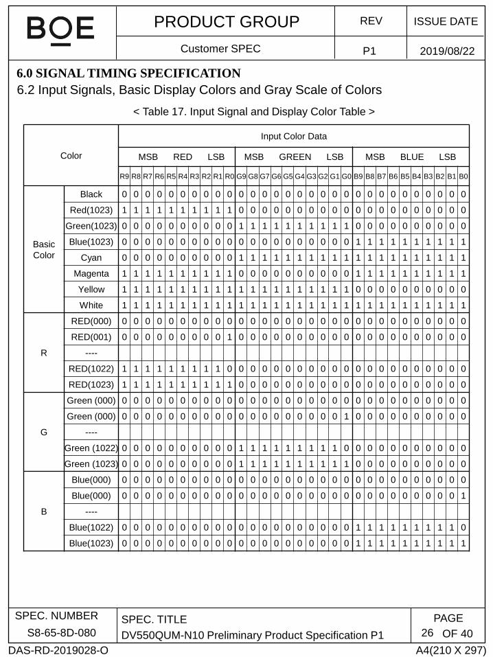
< Table 17. Input Signal and Display Color Table >
Color
Input Color Data
MSB RED LSB MSB GREEN LSB MSB BLUE LSB
R9 R8 R7 R6 R5 R4 R3 R2 R1 R0 G9 G8 G7 G6 G5 G4 G3 G2 G1 G0 B9 B8 B7 B6 B5 B4 B3 B2 B1 B0
Basic
Color
Black 0 0 0 0 0 0 0 0 0 0 0 0 0 0 0 0 0 0 0 0 0 0 0 0 0 0 0 0 0 0
Red(1023) 1 1 1 1 1 1 1 1 1 1 0 0 0 0 0 0 0 0 0 0 0 0 0 0 0 0 0 0 0 0
Green(1023) 0 0 0 0 0 0 0 0 0 0 1 1 1 1 1 1 1 1 1 1 0 0 0 0 0 0 0 0 0 0
Blue(1023) 0 0 0 0 0 0 0 0 0 0 0 0 0 0 0 0 0 0 0 0 1 1 1 1 1 1 1 1 1 1
Cyan 0 0 0 0 0 0 0 0 0 0 1 1 1 1 1 1 1 1 1 1 1 1 1 1 1 1 1 1 1 1
Magenta 1 1 1 1 1 1 1 1 1 1 0 0 0 0 0 0 0 0 0 0 1 1 1 1 1 1 1 1 1 1
Yellow 1 1 1 1 1 1 1 1 1 1 1 1 1 1 1 1 1 1 1 1 0 0 0 0 0 0 0 0 0 0
White 1 1 1 1 1 1 1 1 1 1 1 1 1 1 1 1 1 1 1 1 1 1 1 1 1 1 1 1 1 1
R
RED(000) 0 0 0 0 0 0 0 0 0 0 0 0 0 0 0 0 0 0 0 0 0 0 0 0 0 0 0 0 0 0
RED(001) 0 0 0 0 0 0 0 0 0 1 0 0 0 0 0 0 0 0 0 0 0 0 0 0 0 0 0 0 0 0
----
RED(1022) 1 1 1 1 1 1 1 1 1 0 0 0 0 0 0 0 0 0 0 0 0 0 0 0 0 0 0 0 0 0
RED(1023) 1 1 1 1 1 1 1 1 1 1 0 0 0 0 0 0 0 0 0 0 0 0 0 0 0 0 0 0 0 0
G
Green (000) 0 0 0 0 0 0 0 0 0 0 0 0 0 0 0 0 0 0 0 0 0 0 0 0 0 0 0 0 0 0
Green (000) 0 0 0 0 0 0 0 0 0 0 0 0 0 0 0 0 0 0 0 1 0 0 0 0 0 0 0 0 0 0
----
Green (1022) 0 0 0 0 0 0 0 0 0 0 1 1 1 1 1 1 1 1 1 0 0 0 0 0 0 0 0 0 0 0
Green (1023) 0 0 0 0 0 0 0 0 0 0 1 1 1 1 1 1 1 1 1 1 0 0 0 0 0 0 0 0 0 0
B
Blue(000) 0 0 0 0 0 0 0 0 0 0 0 0 0 0 0 0 0 0 0 0 0 0 0 0 0 0 0 0 0 0
Blue(000) 0 0 0 0 0 0 0 0 0 0 0 0 0 0 0 0 0 0 0 0 0 0 0 0 0 0 0 0 0 1
----
Blue(1022) 0 0 0 0 0 0 0 0 0 0 0 0 0 0 0 0 0 0 0 0 1 1 1 1 1 1 1 1 1 0
Blue(1023) 0 0 0 0 0 0 0 0 0 0 0 0 0 0 0 0 0 0 0 0 1 1 1 1 1 1 1 1 1 1
6.2 Input Signals, Basic Display Colors and Gray Scale of Colors
6.0 SIGNAL TIMING SPECIFICATION

A4(210 X 297)
PAGE
REV ISSUE DATEPRODUCT GROUP
Customer SPEC
OF 40
SPEC. TITLE
DV550QUM-N10 Preliminary Product Specification P1
DAS-RD-2019028-O
SPEC. NUMBER
S8-65-8D-080
P1 2019/08/22
27
6.3 Power Sequence
< Table 18. Sequence Table >
ParameterValues
UnitsMin Typ Max
T1 0.5 - 10 ms
T2 0 - - ms
T3 200 - - ms
T4 100 - - ms
T5 0 - - ms
T6 1 - - s
T7 - - 200 ms
T8 1200 - - ms
T9 Depends on I2C command ms
Power Supply
VDD
Interface Signal
( Input Data )
LOCKN
HOST I2C
Command
BLU ON/OFF
enable
( VON/OFF )
0V
12V
0.1VDD
0.9VDD
T1
T2
24V
T3
0.9VDD
0.1VDD
T5T6
0V
0V
0V
T7
T8
T9
Active SignalHi-Z Hi-Z
T4
Notes: 1. Even though T1 is over the specified value, there is no problem if I2T spec of fuse is satisfied.
2. Back Light must be turn on after power for logic and interface signal are valid.
6.0 SIGNAL TIMING SPECIFICATION

A4(210 X 297)
PAGE
REV ISSUE DATEPRODUCT GROUP
Customer SPEC
OF 40
SPEC. TITLE
DV550QUM-N10 Preliminary Product Specification P1
DAS-RD-2019028-O
SPEC. NUMBER
S8-65-8D-080
P1 2019/08/22
7.0 OPTICAL SPECIFICATION
The test of optical specifications shall be measured in a dark room (ambient luminance1 lux
and temperature=252℃) with the equipment of Luminance meter system (Goniometer
system and PR730) and test unit shall be located at an approximate distance 180cm from
the LCD surface at a viewing angle of θ and Φ equal to 0. We refer to θØ=0 (=θ3 ) as the 3
o’clock direction (the “right”), θØ=90 (= θ12 ) as the 12 o’clock direction (“upward”), θØ=180 (= θ9 )
as the 9 o’clock direction (“left”) and θØ=270(= θ6 ) as the 6 o’clock direction (“bottom”). While
scanning θ and/or Ø, the center of the measuring spot on the Display surface shall stay fixed.
The measurement shall be executed after 30 minutes warm-up period. VDD shall be 12.0V
+/-10% at 25C. Optimum viewing angle direction is 6 ’clock.
Parameter Symbol Condition Min Typ Max Unit Remark
Viewing
Angle
Horizont
al
Θ3
CR > 10
- 89 - Deg.
Note 1Θ9 - 89 - Deg.
VerticalΘ12 - 89 - Deg.
Θ6 - 89 - Deg.
Contrast ratio CR
Θ = 0
(Center)
Normal
Viewing
Angle
1000:1 1200:1 - - Note 2
Reproduction
of color
WhiteWx
TYP.
- 0.03
0.280
TYP.
+ 0.03
-
Note 3
Wy 0.290 -
RedRx 0.641 -
Ry 0.340 -
GreenGx 0.302 -
Gy 0.619 -
BlueBx 0.154 -
By 0.052 -
Response Time G to G Tg - 8 10 ms Note 4
Gamma Scale 2.0 2.2 2.4 -
2.2± 0.3
(50~128
Gray)
Cell Transmittance 4.8 5.4 - % Note 5
Surface Luminance, white L WH 720 800 - cd/m2 Note 6
Luminance Variation δWHITE gP 70 75 - % Note 7
[VDD = 12.0V, Frame rate = 60Hz, Ta =25± 2 ℃]
< Table 19. Optical Table >
28

A4(210 X 297)
PAGE
REV ISSUE DATEPRODUCT GROUP
Customer SPEC
OF 40
SPEC. TITLE
DV550QUM-N10 Preliminary Product Specification P1
DAS-RD-2019028-O
SPEC. NUMBER
S8-65-8D-080
P1 2019/08/22
29
Note :
1. Viewing angle is the angle at which the contrast ratio is greater than 10. The viewing are
determined for the horizontal or 3, 9 o’clock direction and the vertical or 6, 12 o’clock
direction with respect to the optical axis which is normal to the LCD surface.
2. Contrast measurements shall be made at viewing angle of = 0 and at the center of the LCD
surface. Luminance shall be measured with all pixels in the view field set first to white, then
to the dark (black) state. (See Figure 1 shown in Appendix) Luminance Contrast Ratio (CR)
is defined mathematically.
Luminance when displaying a white raster
Luminance when displaying a black raster
3. The color chromaticity coordinates specified in Table 187shall be calculated from the spectral
data measured with all pixels first in red, green, blue. Measurements shall be
made at the center of the panel. The BLU is used by BOE.
4. Response time Tg is the average time required for display transition by switching the input
signal as below table and is based on Frame rate fV =60Hz to optimize.
Each time in below table is defined as Figure 2 and shall be measured by switching the input
signal for “any level of gray(bright)”and “any level of gray(dark)”
CR =
5. Definition of Transmittance (T%) :
Module is with white(L255) signal input
Transmittance = Luminance of LCD Module
Luminance of BLU× 100 %
A4(210 X 297)
PAGE
REV ISSUE DATEPRODUCT GROUP
Customer SPEC
OF 40
SPEC. TITLE
DV550QUM-N10 Preliminary Product Specification P1
DAS-RD-2019028-O
SPEC. NUMBER
S8-65-8D-080
P1 2019/08/22
30
Note :
6. Surface luminance are determined after the unit has been ‘ON’ and 1 Hour after lighting the
backlight in a dark environment at 25± 2℃. Surface luminance is the luminance value at
center 1-point across the LCD surface 50cm from the surface with all pixels displaying white.
7. The variation in surface luminance, δ WHITE is define as:
δ WHITE(9P)=Minimum(Lon1,Lon2,Lon3,Lon4,Lon0)/Maximum(Lon1,Lon2,Lon3,Lon4,Lon9)
Where Lon1 to Lon9 are the luminance with all pixels displaying while at 9 locations.
For more information, see the Figure 3(located in Appendix).

A4(210 X 297)
PAGE
REV ISSUE DATEPRODUCT GROUP
Customer SPEC
OF 40
SPEC. TITLE
DV550QUM-N10 Preliminary Product Specification P1
DAS-RD-2019028-O
SPEC. NUMBER
S8-65-8D-080
P1 2019/08/22
31
8.0 MECHANICAL CHARACTERISTICS
8.1 Dimensional Requirements
Figure 4(located in Appendix) shows mechanical outlines for the model DV550QUM-N10.
Other parameters are shown in Table 20.
Parameter Specification Unit
Active area 1209.6 (H) × 680.4(V) mm
Pixel pitch 315 (H) × 315 (V) μm
Number of pixels 3840(H) × 2160(V) (TFT pixel)
3840(H) × 2160(V) (1 CF pixel= R + G + B dots)pixels
MDL Dimensional
outline1232.4(H) x 703.2(V) x 17(B) mm
Weight 15 kg
< Table 20. Dimensional Parameters >
8.2 Mounting
See Figure 5. (Shown in Appendix)
8.3 Anti-Glare and Polarizer Hardness
The surface of the LCD has an low haze coating to reduce scratching. Front Polarizer
hardness is at less 3H.

A4(210 X 297)
PAGE
REV ISSUE DATEPRODUCT GROUP
Customer SPEC
OF 40
SPEC. TITLE
DV550QUM-N10 Preliminary Product Specification P1
DAS-RD-2019028-O
SPEC. NUMBER
S8-65-8D-080
P1 2019/08/22
32
9.0 RELIABILITY TEST
The Reliability test items and its conditions are shown in below.
No Test Items Conditions
1 High temperature storage test Ta = 60 ℃, 240 hrs
2 Low temperature storage test Ta = -20 ℃, 240 hrs
3 High temperature & high
humidity operation test
Ta = 50 ℃, 80%RH, 240hrs
4 High temperature operation test Ta = 50 ℃, 240hrs
5 Low temperature operation test Ta = -5 ℃, 240hrs
6 Thermal shock Ta = -20 ℃ ↔ 60 ℃ (0.5 hr), 100 cycle
7 Packing VIB 1.20Grms, 1-200Hz, Random +Z 1hr
8 Electro-static discharge test Air : ± 15kV ,150pF/330Ω ,100Point ,1time/Point
Contact :
± 8kV ,150pF/330Ω ,100Point ,1time/Point
Non operation
Contact:± 4KV~± 6KV,150pF/330Ω,100Point,
Input connector Pin, 3 times/pin with no function
loss
< Table 21. Reliability Test Parameters >

A4(210 X 297)
PAGE
REV ISSUE DATEPRODUCT GROUP
Customer SPEC
OF 40
SPEC. TITLE
DV550QUM-N10 Preliminary Product Specification P1
DAS-RD-2019028-O
SPEC. NUMBER
S8-65-8D-080
P1 2019/08/22
33
10.0 HANDLING & CAUTIONS
(1) Cautions when taking out the Panel
Pick the pouch only, when taking out panel from a shipping package.
(2) Cautions for handling the panel
As the electrostatic discharges may break the LCD panel, handle the LCD
panel with care. Peel a protection sheet off from the LCD panel surface as
slowly as possible.
As the LCD panel and back - light element are made from fragile glass material,
impulse and pressure to the LCD panel should be avoided.
As the surface of the polarizer is very soft and easily scratched, use a soft dry
cloth without chemicals for cleaning.
Do not pull the interface connector in or out while the LCD panel is operating.
Put the panel display side down on a flat horizontal plane.
Handle connectors and cables with care.
(3) Cautions for the operation
When the panel is operating, do not lose CLK, ENAB signals. If any one of
these signals is lost, the LCD panel would be damaged.
Obey the supply voltage sequence. If wrong sequence is applied, the panel
would be damaged.
(4) Cautions for the atmosphere
Dew drop atmosphere should be avoided.
Do not store and/or operate the LCD panel in a high temperature and/or
humidity atmosphere. Storage in an electro-conductive polymer packing pouch
and under relatively low temperature atmosphere is recommended.
(5) Cautions for the panel characteristics
Do not apply fixed pattern data signal to the LCD panel at product aging.
Applying fixed pattern for a long time may cause image sticking.
(6) Other cautions
Do not disassemble and/or re-assemble LCD panel.
Do not re-adjust variable resistor or switch etc.
When returning the panel for repair or etc., Please pack the panel not to be
broken. We recommend to use the original shipping packages.

A4(210 X 297)
PAGE
REV ISSUE DATEPRODUCT GROUP
Customer SPEC
OF 40
SPEC. TITLE
DV550QUM-N10 Preliminary Product Specification P1
DAS-RD-2019028-O
SPEC. NUMBER
S8-65-8D-080
P1 2019/08/22
34
11.0 PRODUCT SERIAL NUMBER
XXXX
XXXXXX
XXXXXXXX-XXX
XX-XXXXXX-XXXXX-XXX-XXXX
XXXX
B10
XXXXXXXXXXXXXXXXXX
Module ID 条形码
PP ID 条形码
1
2
3
4
5
打印内容,说明如下:
① FG-CODE
② Module ID,最后一位为Revision Code(扫描不显示), 前17位编码规则如下
③ PPID(客户端ID)
④ D/PN码, 规格待确定
⑤ 生产年份+生产周别(中间无空格)
Module ID编码原则
Digit 1 2 3 4 5 6 7 8 9 10 11 12 13 14 15 16 17
Code S L S A 1 0 8 5 9 4 2 0 0 0 1 D B
Description
Product Cod
e/GBN→
FG-CODE一一对应
Grade line Year Month
Model Extension Code
(Last 4 Digits of FG-CODE
)
Serial No.
Hex-Decimal
000000-FFFFFF
Label Size : 80 mm (L) 25 mm (W)
Label Picture:
A4(210 X 297)
PAGE
REV ISSUE DATEPRODUCT GROUP
Customer SPEC
OF 40
SPEC. TITLE
DV550QUM-N10 Preliminary Product Specification P1
DAS-RD-2019028-O
SPEC. NUMBER
S8-65-8D-080
P1 2019/08/22
35
12.0 PACKING
BOE provides the standard shipping container for customers, unless customer specifies
their packing information. The standard packing method and Barcode information are
shown in below.
12.2 Packing Method
12.1 Packing Specifications
8 LCD TV modules/ 1 Box
Box dimensions: 1370(L) x565(W) x787(H)mm
Weight: approximately 126Kg (8 modules per box)
2 Boxes / 1 Pallet
Pallet dimensions : 1390(L) x1150(W) x901(H)mm (with boxes)
A4(210 X 297)
PAGE
REV ISSUE DATEPRODUCT GROUP
Customer SPEC
OF 40
SPEC. TITLE
DV550QUM-N10 Preliminary Product Specification P1
DAS-RD-2019028-O
SPEC. NUMBER
S8-65-8D-080
P1 2019/08/22
36
12.3 Box Label
Label Size : 100 mm (L) 50 mm (W)
Contents
Model : DV550QUM-N10 (FG-CODE)
Q`ty : 8 Module in one box.
Serial No. : Box Serial No.
Date : Packing Date
FG Code : FG Code of Product
XXXXXXXX-XXX
XXXXXXXXXXXXX
XXX
XXXX.XX.XX
XXXX
1 2
3 4
5
Box ID 条形码
XXXXXXXXXXXX 6
打印内容,说明如下:
① FG-CODE
② 产品数量
③ Box ID, 编码规则如下
④ Box Packing 日期
⑤ 产品物料号(客户端)
⑥ FG-CODE 后四位
BOX ID 编码原则
Digit 1 2 3 4 5 6 7 8 9 10 11 12 13
Code S L S A 1 6 3 D 0 0 1 A 1
DescriptionProducts
GBNGrade Line Year Month
Revision
CodeSerial No.
RoHS Mark
Label Picture:
(L1390*1150*114mm)
Sea/ Land Transportation Air Transportation
(L1390*1150*114mm)

A4(210 X 297)
PAGE
REV ISSUE DATEPRODUCT GROUP
Customer SPEC
OF 40
SPEC. TITLE
DV550QUM-N10 Preliminary Product Specification P1
DAS-RD-2019028-O
SPEC. NUMBER
S8-65-8D-080
P1 2019/08/22
37
13.0 APPENDIX
< Figure 1. Measurement Set Up >
< Figure 2. Response Time Testing >

A4(210 X 297)
PAGE
REV ISSUE DATEPRODUCT GROUP
Customer SPEC
OF 40
SPEC. TITLE
DV550QUM-N10 Preliminary Product Specification P1
DAS-RD-2019028-O
SPEC. NUMBER
S8-65-8D-080
P1 2019/08/22
38
< Figure 3. Point for Luminance Measure>
13.0 APPENDIX
A:H/9 mm
B:V/9 mm
@H,V:Active Area
V/2
H/2A
H
B
V
42 3
65 1
97 8
Measuring point for surface luminance & luminance variationCA-310 ,Contact method

A4(210 X 297)
PAGE
REV ISSUE DATEPRODUCT GROUP
Customer SPEC
OF 40
SPEC. TITLE
DV550QUM-N10 Preliminary Product Specification P1
DAS-RD-2019028-O
SPEC. NUMBER
S8-65-8D-080
P1 2019/08/22
39
< Figure 5. TFT-LCD Module Outline Dimensions (Rear View) >
< Figure 4. TFT-LCD Module Outline Dimensions (Front View) >
13.0 APPENDIX

A4(210 X 297)
PAGE
REV ISSUE DATEPRODUCT GROUP
Customer SPEC
OF 40
SPEC. TITLE
DV550QUM-N10 Preliminary Product Specification P1
DAS-RD-2019028-O
SPEC. NUMBER
S8-65-8D-080
P1 2019/08/22
40
(a)This Product is Reverse type display Mode
DV550QUM-N10
CPCBA
1 51
1 60 1 60
60 1 60 1
X-PCB_L X-PCB_R
13.0 APPENDIX
1. Panel scan direction is from top to bottom.
2. Driver data latch direction is from right to left.
Recommended