Integrated, Dual RF Transceiver with Observation Path
Data Sheet AD9375
Rev. 0 Document Feedback Information furnished by Analog Devices is believed to be accurate and reliable. However, no responsibility is assumed by Analog Devices for its use, nor for any infringements of patents or other rights of third parties that may result from its use. Specifications subject to change without notice. No license is granted by implication or otherwise under any patent or patent rights of Analog Devices. Trademarks and registered trademarks are the property of their respective owners.
One Technology Way, P.O. Box 9106, Norwood, MA 02062-9106, U.S.A. Tel: 781.329.4700 ©2017 Analog Devices, Inc. All rights reserved. Technical Support www.analog.com
FEATURES Dual differential Tx Dual differential Rx Observation receiver with 2 inputs Fully integrated, ultralow power DPD actuator and adaptation
engine for PA linearization Sniffer receiver with 3 inputs Tunable range: 300 MHz to 6000 MHz Linearization signal BW to 40 MHz Tx synthesis BW to 250 MHz Rx BW: 8 MHz to 100 MHz Supports FDD and TDD operation Fully integrated independent fractional-N RF synthesizers for
Tx, Rx, ORx, and clock generation JESD204B digital interface
APPLICATIONS 3G/4G small cell base transceiver station (BTS) 3G/4G massive MIMO/active antenna systems
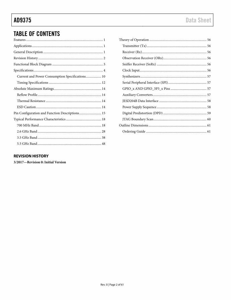
GENERAL DESCRIPTION The AD9375 is a highly integrated, wideband radio frequency (RF) transceiver offering dual-channel transmitters (Tx) and receivers (Rx), integrated synthesizers, a fully integrated digital predistortion (DPD) actuator and adaptation engine, and digital signal processing functions. The IC delivers a versatile combination of high performance and low power consumption required by 3G/4G small cell and massive multiple input, multiple output (MIMO) equipment in both frequency division duplex (FDD) and time division duplex (TDD) applications. The AD9375 operates from 300 MHz to 6000 MHz, covering most of the licensed and unlicensed cellular bands. The DPD algorithm supports linearization on signal bandwidths up to 40 MHz depending on the power amplifier (PA) characteristics (for example, two adjacent 20 MHz carriers). The IC supports Rx bandwidths up to 100 MHz. It also supports observation receiver (ORx) and Tx synthesis bandwidths up to 250 MHz to accommodate digital correction algorithms.
The transceiver consists of wideband direct conversion signal paths with state-of-the-art noise figure and linearity. Each complete Rx and Tx subsystem includes dc offset correction, quadrature error correction (QEC), and programmable digital filters, eliminating the need for these functions in the digital baseband. Several auxiliary functions such as an auxiliary analog-to-digital converter (ADC), auxiliary digital-to-analog converters (DACs), and general-purpose input/outputs (GPIOs) are integrated to provide additional monitoring and control capability.
An ORx channel with two inputs is included to monitor each Tx output and implement calibration applications. This channel also connects to three sniffer receiver (SnRx) inputs that can monitor radio activity in different bands.
The high speed JESD204B interface supports lane rates up to 6144 Mbps. Four lanes are dedicated to the transmitters and four lanes are dedicated to the receiver and observation receiver channels.
The fully integrated phase-locked loops (PLLs) provide high performance, low power, fractional-N frequency synthesis for the Tx, the Rx, the ORx, and the clock sections. Careful design and layout techniques provide the isolation demanded in high performance base station applications. All voltage controlled oscillator (VCO) and loop filter components are integrated to minimize the external component count.
The device contains a fully integrated, low power DPD actuator and adaptation engine for use in PA linearization. The DPD feature enables use of high efficiency PAs, significantly reducing the power consumption of small cell base station radios while also reducing the number of JESD204B lanes necessary to interface with baseband processors.
A 1.3 V supply is required to power the AD9375 core, and a standard 4-wire serial port controls it. Other voltage supplies provide proper digital interface levels and optimize transmitter and auxiliary converter performance. The AD9375 is packaged in a 12 mm × 12 mm, 196-ball chip scale ball grid array (CSP_BGA).
AD9375 Data Sheet
Rev. 0 | Page 2 of 61
TABLE OF CONTENTS Features .............................................................................................. 1 Applications ....................................................................................... 1 General Description ......................................................................... 1 Revision History ............................................................................... 2 Functional Block Diagram .............................................................. 3 Specifications ..................................................................................... 4
Current and Power Consumption Specifications................... 10 Timing Specifications ................................................................ 12
Absolute Maximum Ratings .......................................................... 14 Reflow Profile .............................................................................. 14 Thermal Resistance .................................................................... 14 ESD Caution ................................................................................ 14
Pin Configuration and Function Descriptions ........................... 15 Typical Performance Characteristics ........................................... 18
700 MHz Band ............................................................................ 18 2.6 GHz Band .............................................................................. 28 3.5 GHz Band .............................................................................. 38 5.5 GHz Band .............................................................................. 48
Theory of Operation ...................................................................... 56 Transmitter (Tx) ......................................................................... 56 Receiver (Rx) ............................................................................... 56 Observation Receiver (ORx) ..................................................... 56 Sniffer Receiver (SnRx) ............................................................. 56 Clock Input.................................................................................. 56 Synthesizers ................................................................................. 57 Serial Peripheral Interface (SPI) ............................................... 57 GPIO_x AND GPIO_3P3_x Pins ............................................ 57 Auxiliary Converters .................................................................. 57 JESD204B Data Interface .......................................................... 58 Power Supply Sequence ............................................................. 58 Digital Predistortion (DPD) ..................................................... 59 JTAG Boundary Scan ................................................................. 60
Outline Dimensions ....................................................................... 61 Ordering Guide .......................................................................... 61
REVISION HISTORY 3/2017—Revision 0: Initial Version
Data Sheet AD9375
Rev. 0 | Page 3 of 61
FUNCTIONAL BLOCK DIAGRAM
OBSERVATIONRxORX1+
ORX1–
ORX2+ORX2–
JESD204B
JESD204B
JESD204B
DEV_CLK_IN+,DEV_CLK_IN–
RX_EXTLO+RX_EXTLO–
ADCLPFRx2
ADCLPF
Rx1RX1+
RX1–
LOGENERATOR
RFSYNTHESIZER
RX2+
RX2–
DECIMATION,pFIR, AGC,DC OFFSET
QEC,TUNING,
RSSI,OVERLOAD
MICRO-CONTROLLER
SPISPIPORT
CTRL INTCONTROLINTERFACE
ADCLPF
SNIFFERRx
ADCLPF
TX_EXTLO+TX_EXTLO–
DACLPFTx2
DACLPF
Tx1TX1+
TX1–
TX2+
TX2–pFIR,
DC OFFSET,QEC, TUNNING,
INTER-POLATION
GPIOAUXADCAUXDAC
CLOCKGENERATOR
EXTERNALOPTION
LOGENERATOR
RFSYNTHESIZER
RFSYNTHESIZER
LOGENERATOR
EXTERNALOPTION
SNRXA+SNRXA–SNRXB+SNRXB–SNRXC+SNRXC–
DECIMATION,pFIR,AGC,
DC OFFSET,QEC,
TUNING,RSSI,
OVERLOAD
AD9375
DPD
1565
7-00
1
Figure 1.
AD9375 Data Sheet
Rev. 0 | Page 4 of 61
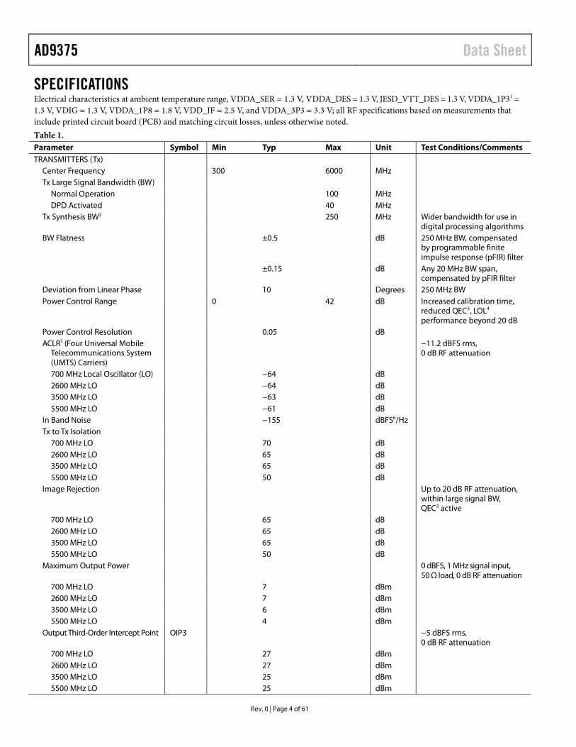
SPECIFICATIONS Electrical characteristics at ambient temperature range, VDDA_SER = 1.3 V, VDDA_DES = 1.3 V, JESD_VTT_DES = 1.3 V, VDDA_1P31 = 1.3 V, VDIG = 1.3 V, VDDA_1P8 = 1.8 V, VDD_IF = 2.5 V, and VDDA_3P3 = 3.3 V; all RF specifications based on measurements that include printed circuit board (PCB) and matching circuit losses, unless otherwise noted. Table 1. Parameter Symbol Min Typ Max Unit Test Conditions/Comments TRANSMITTERS (Tx)
Center Frequency 300 6000 MHz Tx Large Signal Bandwidth (BW)
Normal Operation 100 MHz DPD Activated 40 MHz
Tx Synthesis BW2 250 MHz Wider bandwidth for use in digital processing algorithms
BW Flatness ±0.5 dB 250 MHz BW, compensated by programmable finite impulse response (pFIR) filter
±0.15 dB Any 20 MHz BW span, compensated by pFIR filter
Deviation from Linear Phase 10 Degrees 250 MHz BW Power Control Range 0 42 dB Increased calibration time,
reduced QEC3, LOL4 performance beyond 20 dB
Power Control Resolution 0.05 dB ACLR5 (Four Universal Mobile
Telecommunications System (UMTS) Carriers)
−11.2 dBFS rms, 0 dB RF attenuation
700 MHz Local Oscillator (LO) −64 dB 2600 MHz LO −64 dB 3500 MHz LO −63 dB 5500 MHz LO −61 dB
In Band Noise −155 dBFS6/Hz Tx to Tx Isolation
700 MHz LO 70 dB 2600 MHz LO 65 dB 3500 MHz LO 65 dB 5500 MHz LO 50 dB
Image Rejection Up to 20 dB RF attenuation, within large signal BW, QEC3 active
700 MHz LO 65 dB 2600 MHz LO 65 dB 3500 MHz LO 65 dB 5500 MHz LO 50 dB
Maximum Output Power 0 dBFS, 1 MHz signal input, 50 Ω load, 0 dB RF attenuation
700 MHz LO 7 dBm 2600 MHz LO 7 dBm 3500 MHz LO 6 dBm 5500 MHz LO 4 dBm
Output Third-Order Intercept Point OIP3 −5 dBFS rms, 0 dB RF attenuation
700 MHz LO 27 dBm 2600 MHz LO 27 dBm 3500 MHz LO 25 dBm 5500 MHz LO 25 dBm
Data Sheet AD9375
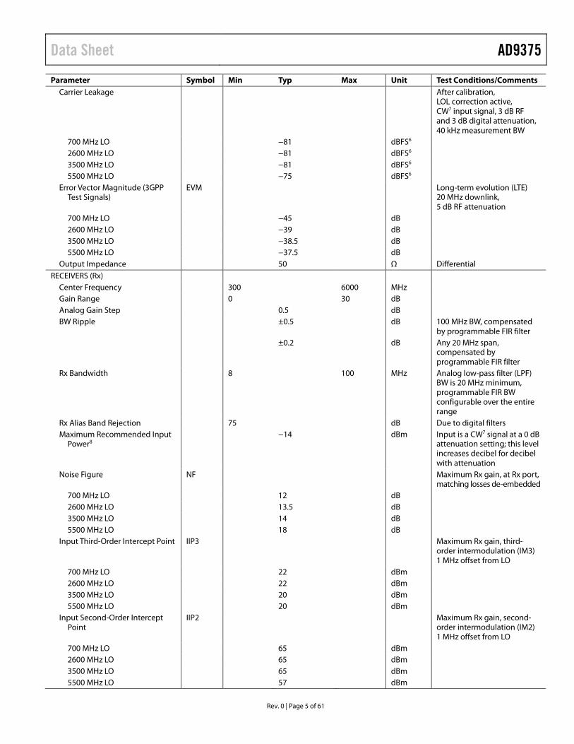
Rev. 0 | Page 5 of 61
Parameter Symbol Min Typ Max Unit Test Conditions/Comments Carrier Leakage After calibration,
LOL correction active, CW7 input signal, 3 dB RF and 3 dB digital attenuation, 40 kHz measurement BW
700 MHz LO −81 dBFS6 2600 MHz LO −81 dBFS6 3500 MHz LO −81 dBFS6 5500 MHz LO −75 dBFS6
Error Vector Magnitude (3GPP Test Signals)
EVM Long-term evolution (LTE) 20 MHz downlink, 5 dB RF attenuation
700 MHz LO −45 dB 2600 MHz LO −39 dB 3500 MHz LO −38.5 dB 5500 MHz LO −37.5 dB
Output Impedance 50 Ω Differential RECEIVERS (Rx)
Center Frequency 300 6000 MHz Gain Range 0 30 dB Analog Gain Step 0.5 dB BW Ripple ±0.5 dB 100 MHz BW, compensated
by programmable FIR filter ±0.2 dB Any 20 MHz span,
compensated by programmable FIR filter
Rx Bandwidth 8 100 MHz Analog low-pass filter (LPF) BW is 20 MHz minimum, programmable FIR BW configurable over the entire range
Rx Alias Band Rejection 75 dB Due to digital filters Maximum Recommended Input
Power8 −14 dBm Input is a CW7 signal at a 0 dB
attenuation setting; this level increases decibel for decibel with attenuation
Noise Figure NF Maximum Rx gain, at Rx port, matching losses de-embedded
700 MHz LO 12 dB 2600 MHz LO 13.5 dB 3500 MHz LO 14 dB 5500 MHz LO 18 dB
Input Third-Order Intercept Point IIP3 Maximum Rx gain, third-order intermodulation (IM3) 1 MHz offset from LO
700 MHz LO 22 dBm 2600 MHz LO 22 dBm 3500 MHz LO 20 dBm 5500 MHz LO 20 dBm
Input Second-Order Intercept Point
IIP2 Maximum Rx gain, second-order intermodulation (IM2) 1 MHz offset from LO
700 MHz LO 65 dBm 2600 MHz LO 65 dBm 3500 MHz LO 65 dBm 5500 MHz LO 57 dBm
AD9375 Data Sheet
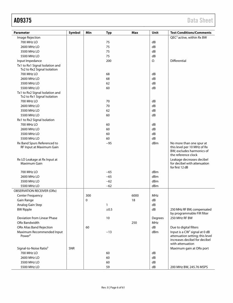
Rev. 0 | Page 6 of 61
Parameter Symbol Min Typ Max Unit Test Conditions/Comments Image Rejection QEC3 active, within Rx BW
700 MHz LO 75 dB 2600 MHz LO 75 dB 3500 MHz LO 75 dB 5500 MHz LO 75 dB
Input Impedance 200 Ω Differential Tx1 to Rx1 Signal Isolation and
Tx2 to Rx2 Signal Isolation
700 MHz LO 68 dB 2600 MHz LO 68 dB 3500 MHz LO 62 dB 5500 MHz LO 60 dB
Tx1 to Rx2 Signal Isolation and Tx2 to Rx1 Signal Isolation
700 MHz LO 70 dB 2600 MHz LO 70 dB 3500 MHz LO 62 dB 5500 MHz LO 60 dB
Rx1 to Rx2 Signal Isolation 700 MHz LO 60 dB 2600 MHz LO 60 dB 3500 MHz LO 60 dB 5500 MHz LO 60 dB
Rx Band Spurs Referenced to RF Input at Maximum Gain
−95 dBm No more than one spur at this level per 10 MHz of Rx BW; excludes harmonics of the reference clock
Rx LO Leakage at Rx Input at Maximum Gain
Leakage decreases decibel for decibel with attenuation for first 12 dB
700 MHz LO −65 dBm 2600 MHz LO −65 dBm 3500 MHz LO −62 dBm 5500 MHz LO −62 dBm
OBSERVATION RECEIVER (ORx) Center Frequency 300 6000 MHz Gain Range 0 18 dB Analog Gain Step 1 dB BW Ripple ±0.5 dB 250 MHz RF BW, compensated
by programmable FIR filter Deviation from Linear Phase 10 Degrees 250 MHz RF BW ORx Bandwidth 250 MHz ORx Alias Band Rejection 60 dB Due to digital filters Maximum Recommended Input
Power8 −13 dBm Input is a CW7 signal at 0 dB
attenuation setting; this level increases decibel for decibel with attenuation
Signal-to-Noise Ratio9 SNR Maximum gain at ORx port 700 MHz LO 60 dB 2600 MHz LO 60 dB 3500 MHz LO 60 dB 5500 MHz LO 59 dB 200 MHz BW, 245.76 MSPS
Data Sheet AD9375
Rev. 0 | Page 7 of 61
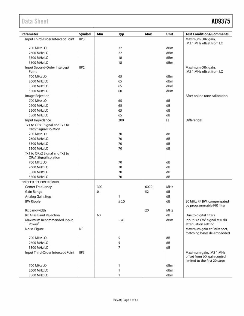
Parameter Symbol Min Typ Max Unit Test Conditions/Comments Input Third-Order Intercept Point IIP3 Maximum ORx gain,
IM3 1 MHz offset from LO 700 MHz LO 22 dBm 2600 MHz LO 22 dBm 3500 MHz LO 18 dBm 5500 MHz LO 18 dBm
Input Second-Order Intercept Point
IIP2 Maximum ORx gain, IM2 1 MHz offset from LO
700 MHz LO 65 dBm 2600 MHz LO 65 dBm 3500 MHz LO 65 dBm 5500 MHz LO 60 dBm
Image Rejection After online tone calibration 700 MHz LO 65 dB 2600 MHz LO 65 dB 3500 MHz LO 65 dB 5500 MHz LO 65 dB
Input Impedance 200 Ω Differential Tx1 to ORx1 Signal and Tx2 to
ORx2 Signal Isolation
700 MHz LO 70 dB 2600 MHz LO 70 dB 3500 MHz LO 70 dB 5500 MHz LO 70 dB
Tx1 to ORx2 Signal and Tx2 to ORx1 Signal Isolation
700 MHz LO 70 dB 2600 MHz LO 70 dB 3500 MHz LO 70 dB 5500 MHz LO 70 dB
SNIFFER RECEIVER (SnRx) Center Frequency 300 6000 MHz Gain Range 0 52 dB Analog Gain Step 1 dB BW Ripple ±0.5 dB 20 MHz RF BW, compensated
by programmable FIR filter Rx Bandwidth 20 MHz Rx Alias Band Rejection 60 dB Due to digital filters Maximum Recommended Input
Power8 −26 dBm Input is a CW7 signal at 0 dB
attenuation setting Noise Figure NF Maximum gain at SnRx port,
matching losses de-embedded 700 MHz LO 5 dB 2600 MHz LO 5 dB 3500 MHz LO 7 dB
Input Third-Order Intercept Point IIP3 Maximum gain, IM3 1 MHz offset from LO, gain control limited to the first 20 steps
700 MHz LO 1 dBm 2600 MHz LO 1 dBm 3500 MHz LO 1 dBm
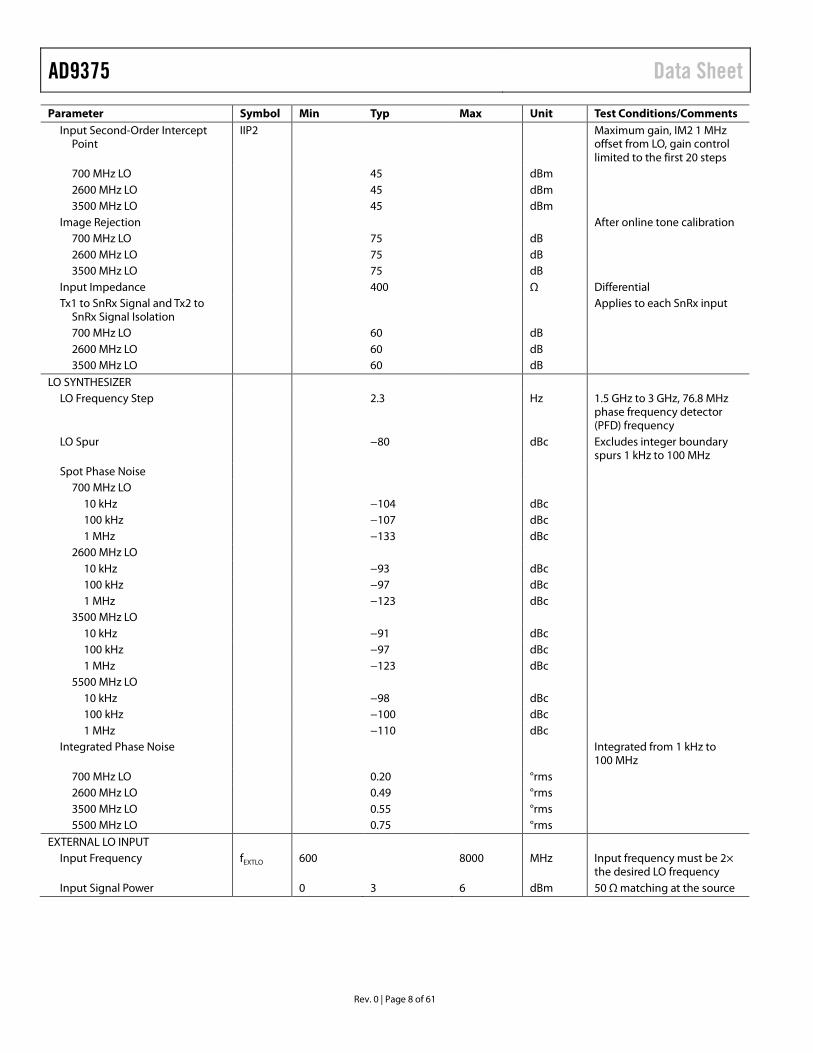
AD9375 Data Sheet
Rev. 0 | Page 8 of 61
Parameter Symbol Min Typ Max Unit Test Conditions/Comments Input Second-Order Intercept
Point IIP2 Maximum gain, IM2 1 MHz
offset from LO, gain control limited to the first 20 steps
700 MHz LO 45 dBm 2600 MHz LO 45 dBm 3500 MHz LO 45 dBm
Image Rejection After online tone calibration 700 MHz LO 75 dB 2600 MHz LO 75 dB 3500 MHz LO 75 dB
Input Impedance 400 Ω Differential Tx1 to SnRx Signal and Tx2 to
SnRx Signal Isolation Applies to each SnRx input
700 MHz LO 60 dB 2600 MHz LO 60 dB 3500 MHz LO 60 dB
LO SYNTHESIZER LO Frequency Step 2.3 Hz 1.5 GHz to 3 GHz, 76.8 MHz
phase frequency detector (PFD) frequency
LO Spur −80 dBc Excludes integer boundary spurs 1 kHz to 100 MHz
Spot Phase Noise 700 MHz LO
10 kHz −104 dBc 100 kHz −107 dBc 1 MHz −133 dBc
2600 MHz LO 10 kHz −93 dBc 100 kHz −97 dBc 1 MHz −123 dBc
3500 MHz LO 10 kHz −91 dBc 100 kHz −97 dBc 1 MHz −123 dBc
5500 MHz LO 10 kHz −98 dBc 100 kHz −100 dBc 1 MHz −110 dBc
Integrated Phase Noise Integrated from 1 kHz to 100 MHz
700 MHz LO 0.20 °rms 2600 MHz LO 0.49 °rms 3500 MHz LO 0.55 °rms 5500 MHz LO 0.75 °rms
EXTERNAL LO INPUT Input Frequency fEXTLO 600 8000 MHz Input frequency must be 2×
the desired LO frequency Input Signal Power 0 3 6 dBm 50 Ω matching at the source
Data Sheet AD9375
Rev. 0 | Page 9 of 61
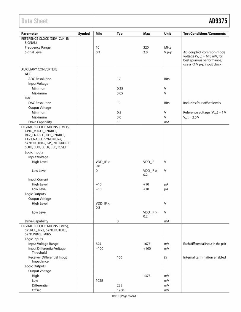
Parameter Symbol Min Typ Max Unit Test Conditions/Comments REFERENCE CLOCK (DEV_CLK_IN
SIGNAL)
Frequency Range 10 320 MHz Signal Level 0.3 2.0 V p-p AC-coupled, common-mode
voltage (VCM) = 618 mV; for best spurious performance, use a <1 V p-p input clock
AUXILIARY CONVERTERS ADC
ADC Resolution 12 Bits Input Voltage
Minimum 0.25 V Maximum 3.05 V
DAC DAC Resolution 10 Bits Includes four offset levels Output Voltage
Minimum 0.5 V Reference voltage (VREF) = 1 V Maximum 3.0 V VREF = 2.5 V
Drive Capability 10 mA DIGITAL SPECIFICATIONS (CMOS),
GPIO_x, RX1_ENABLE, RX2_ENABLE, TX1_ENABLE, TX2 ENABLE, SYNCINBx+, SYNCOUTB0+, GP_INTERRUPT, SDIO, SDO, SCLK, CSB, RESET
Logic Inputs Input Voltage
High Level VDD_IF × 0.8
VDD_IF V
Low Level 0 VDD_IF × 0.2
V
Input Current High Level −10 +10 µA Low Level −10 +10 µA
Logic Outputs Output Voltage
High Level VDD_IF × 0.8
V
Low Level VDD_IF × 0.2
V
Drive Capability 3 mA DIGITAL SPECIFICATIONS (LVDS),
SYSREF_INx±, SYNCOUTB0±, SYNCINBx± PAIRS
Logic Inputs Input Voltage Range 825 1675 mV Each differential input in the pair Input Differential Voltage
Threshold −100 +100 mV
Receiver Differential Input Impedance
100 Ω Internal termination enabled
Logic Outputs Output Voltage
High 1375 mV Low 1025 mV Differential 225 mV Offset 1200 mV
AD9375 Data Sheet
Rev. 0 | Page 10 of 61
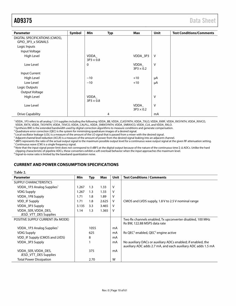
Parameter Symbol Min Typ Max Unit Test Conditions/Comments DIGITAL SPECIFICATIONS (CMOS),
GPIO_3P3_x SIGNALS
Logic Inputs Input Voltage
High Level VDDA_ 3P3 × 0.8
VDDA_3P3 V
Low Level 0 VDDA_ 3P3 × 0.2
V
Input Current High Level −10 +10 µA Low Level −10 +10 µA
Logic Outputs Output Voltage
High Level VDDA_ 3P3 × 0.8
V
Low Level VDDA_ 3P3 × 0.2
V
Drive Capability 4 mA 1 VDDA_1P3 refers to all analog 1.3 V supplies including the following: VDDA_BB, VDDA_CLKSYNTH, VDDA_TXLO, VDDA_RXRF, VDDA_RXSYNTH, VDDA_RXVCO,
VDDA_RXTX, VDDA_TXSYNTH, VDDA_TXVCO, VDDA_CALPLL, VDDA_SNRXSYNTH, VDDA_SNRXVCO, VDDA_CLK, and VDDA_RXLO. 2 Synthesis BW) is the extended bandwidth used by digital correction algorithms to measure conditions and generate compensation. 3 Quadrature error correction (QEC) is the system for minimizing quadrature images of a desired signal. 4 Local oscillator leakage (LOL) is a measure of the amount of the LO signal that is passed from a mixer with the desired signal. 5 Adjacent channel level reduction (ACLR) is a measure of the amount of power from the desired signal leaking into an adjacent channel. 6 dBFS represents the ratio of the actual output signal to the maximum possible output level for a continuous wave output signal at the given RF attenuation setting. 7 Continuous wave (CW) is a single frequency signal. 8 Note that the input signal power limit does not correspond to 0 dBFS at the digital output because of the nature of the continuous time Σ-Δ ADCs. Unlike the hard
clipping characteristic of pipeline ADCs, these converters exhibit a soft overload behavior when the input approaches the maximum level. 9 Signal-to-noise ratio is limited by the baseband quantization noise.
CURRENT AND POWER CONSUMPTION SPECIFICATIONS
Table 2. Parameter Min Typ Max Unit Test Conditions / Comments SUPPLY CHARACTERISTICS
VDDA_1P3 Analog Supplies1 1.267 1.3 1.33 V VDIG Supply 1.267 1.3 1.33 V VDDA_1P8 Supply 1.71 1.8 1.89 V VDD_IF Supply 1.71 1.8 2.625 V CMOS and LVDS supply, 1.8 V to 2.5 V nominal range VDDA_3P3 Supply 3.135 3.3 3.465 V VDDA_SER, VDDA_DES,
JESD_VTT_DES Supplies 1.14 1.3 1.365 V
POSITIVE SUPPLY CURRENT (Rx MODE) Two Rx channels enabled, Tx upconverter disabled, 100 MHz Rx BW, 122.88 MSPS data rate
VDDA_1P3 Analog Supplies1 1055 mA VDIG Supply 625 mA Rx QEC2 enabled, QEC2 engine active VDD_IF Supply (CMOS and LVDS) 8 mA VDDA_3P3 Supply 1 mA No auxiliary DACs or auxiliary ADCs enabled; if enabled, the
auxiliary ADC adds 2.7 mA, and each auxiliary ADC adds 1.5 mA VDDA_SER, VDDA_DES,
JESD_VTT_DES Supplies 375 mA
Total Power Dissipation 2.70 W
Data Sheet AD9375
Rev. 0 | Page 11 of 61
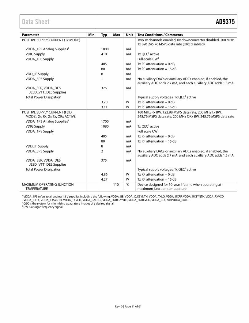
Parameter Min Typ Max Unit Test Conditions / Comments POSITIVE SUPPLY CURRENT (Tx MODE) Two Tx channels enabled, Rx downconverter disabled, 200 MHz
Tx BW, 245.76 MSPS data rate (ORx disabled) VDDA_1P3 Analog Supplies1 1000 mA VDIG Supply 410 mA Tx QEC2 active VDDA_1P8 Supply Full-scale CW3 405 mA Tx RF attenuation = 0 dB, 80 mA Tx RF attenuation = 15 dB VDD_IF Supply 8 mA VDDA_3P3 Supply 1 mA No auxiliary DACs or auxiliary ADCs enabled; if enabled, the
auxiliary ADC adds 2.7 mA, and each auxiliary ADC adds 1.5 mA VDDA_SER, VDDA_DES,
JESD_VTT_DES Supplies 375 mA
Total Power Dissipation Typical supply voltages, Tx QEC2 active 3.70 W Tx RF attenuation = 0 dB 3.11 W Tx RF attenuation = 15 dB POSITIVE SUPPLY CURRENT (FDD
MODE), 2× Rx, 2× Tx, ORx ACTIVE 100 MHz Rx BW, 122.88 MSPS data rate; 200 MHz Tx BW,
245.76 MSPS data rate; 200 MHz ORx BW, 245.76 MSPS data rate VDDA_1P3 Analog Supplies1 1700 mA VDIG Supply 1080 mA Tx QEC2 active VDDA_1P8 Supply Full scale CW3 405 mA Tx RF attenuation = 0 dB 80 mA Tx RF attenuation = 15 dB VDD_IF Supply 8 mA VDDA_3P3 Supply 2 mA No auxiliary DACs or auxiliary ADCs enabled; if enabled, the
auxiliary ADC adds 2.7 mA, and each auxiliary ADC adds 1.5 mA VDDA_SER, VDDA_DES,
JESD_VTT_DES Supplies 375 mA
Total Power Dissipation Typical supply voltages, Tx QEC2 active 4.86 W Tx RF attenuation = 0 dB 4.27 W Tx RF attenuation = 15 dB MAXIMUM OPERATING JUNCTION
TEMPERATURE 110 °C Device designed for 10-year lifetime when operating at
maximum junction temperature 1 VDDA_1P3 refers to all analog 1.3 V supplies including the following: VDDA_BB, VDDA_CLKSYNTH, VDDA_TXLO, VDDA_RXRF, VDDA_RXSYNTH, VDDA_RXVCO,
VDDA_RXTX, VDDA_TXSYNTH, VDDA_TXVCO, VDDA_CALPLL, VDDA_SNRXSYNTH, VDDA_SNRXVCO, VDDA_CLK, and VDDA_RXLO. 2 QEC is the system for minimizing quadrature images of a desired signal. 3 CW is a single frequency signal.
AD9375 Data Sheet
Rev. 0 | Page 12 of 61
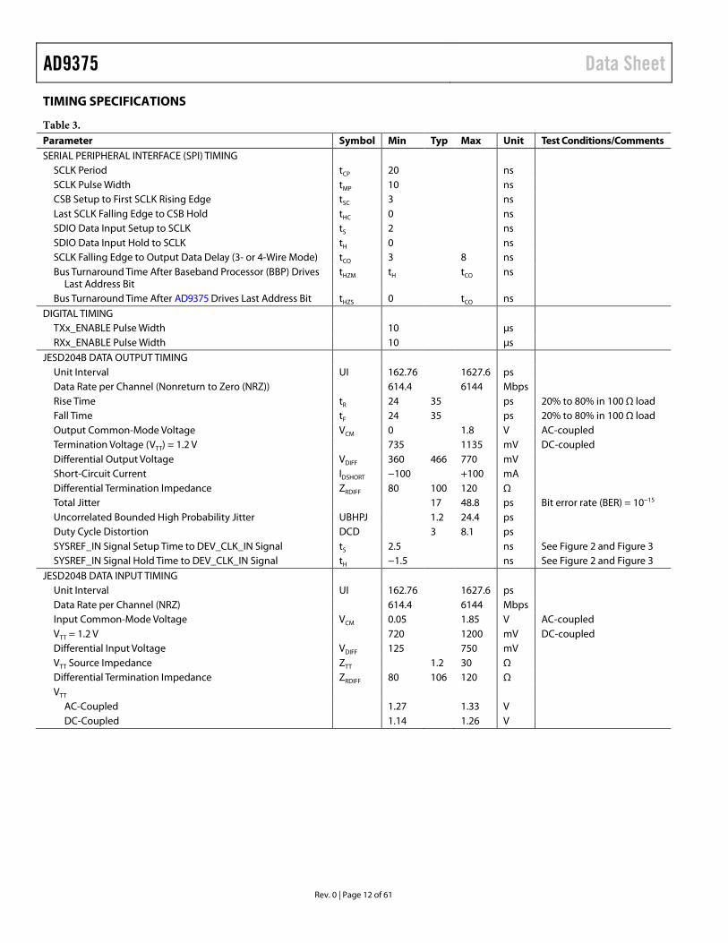
TIMING SPECIFICATIONS
Table 3. Parameter Symbol Min Typ Max Unit Test Conditions/Comments SERIAL PERIPHERAL INTERFACE (SPI) TIMING
SCLK Period tCP 20 ns SCLK Pulse Width tMP 10 ns CSB Setup to First SCLK Rising Edge tSC 3 ns Last SCLK Falling Edge to CSB Hold tHC 0 ns SDIO Data Input Setup to SCLK tS 2 ns SDIO Data Input Hold to SCLK tH 0 ns SCLK Falling Edge to Output Data Delay (3- or 4-Wire Mode) tCO 3 8 ns Bus Turnaround Time After Baseband Processor (BBP) Drives
Last Address Bit tHZM tH tCO ns
Bus Turnaround Time After AD9375 Drives Last Address Bit tHZS 0 tCO ns DIGITAL TIMING
TXx_ENABLE Pulse Width 10 µs RXx_ENABLE Pulse Width 10 µs
JESD204B DATA OUTPUT TIMING Unit Interval UI 162.76 1627.6 ps Data Rate per Channel (Nonreturn to Zero (NRZ)) 614.4 6144 Mbps Rise Time tR 24 35 ps 20% to 80% in 100 Ω load Fall Time tF 24 35 ps 20% to 80% in 100 Ω load Output Common-Mode Voltage VCM 0 1.8 V AC-coupled Termination Voltage (VTT) = 1.2 V 735 1135 mV DC-coupled Differential Output Voltage VDIFF 360 466 770 mV Short-Circuit Current IDSHORT −100 +100 mA Differential Termination Impedance ZRDIFF 80 100 120 Ω Total Jitter 17 48.8 ps Bit error rate (BER) = 10−15 Uncorrelated Bounded High Probability Jitter UBHPJ 1.2 24.4 ps Duty Cycle Distortion DCD 3 8.1 ps SYSREF_IN Signal Setup Time to DEV_CLK_IN Signal tS 2.5 ns See Figure 2 and Figure 3 SYSREF_IN Signal Hold Time to DEV_CLK_IN Signal tH −1.5 ns See Figure 2 and Figure 3
JESD204B DATA INPUT TIMING Unit Interval UI 162.76 1627.6 ps Data Rate per Channel (NRZ) 614.4 6144 Mbps Input Common-Mode Voltage VCM 0.05 1.85 V AC-coupled VTT = 1.2 V 720 1200 mV DC-coupled Differential Input Voltage VDIFF 125 750 mV VTT Source Impedance ZTT 1.2 30 Ω Differential Termination Impedance ZRDIFF 80 106 120 Ω VTT
AC-Coupled 1.27 1.33 V DC-Coupled 1.14 1.26 V
Data Sheet AD9375
Rev. 0 | Page 13 of 61
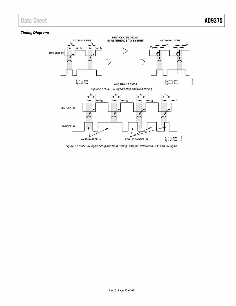
Timing Diagrams
AT DEVICE PINS
DEV_CLK_IN
tH = –1.5nstS = +2.5ns
t'H = +0.5nst'S = +0.5ns
AT DIGITAL CORE
tH
tS
tH
tS t'Ht'St'H
DEV_CLK_IN DELAYIN REFERENCE TO SYSREF
CLK DELAY = 2ns 1565
7-00
2
Figure 2. SYSREF_IN Signal Setup and Hold Timing
DEV_CLK_IN
SYSREF_IN
VALID SYSREF_INtH = –1.5nstS = +2.5ns
tH
tS
tH
tS
tH
tS
tH
tS
INVALID SYSREF_IN
1565
7-00
3
Figure 3. SYSREF_IN Signal Setup and Hold Timing Examples Relative to DEV_CLK_IN Signal
AD9375 Data Sheet
Rev. 0 | Page 14 of 61
ABSOLUTE MAXIMUM RATINGS Table 4. Parameter Rating VDDA_1P31 to VSSA −0.3 V to +1.4 V VDDA_SER, VDDA_DES, and
JESD_VTT_DES to VSSA −0.3 V to +1.4 V
VDIG to VSSD −0.3 V to +1.4 V VDDA_1P8 to VSSA −0.3 V to +2.0 V VDD_IF to VSSA −0.3 V to +3.0 V VDDA_3P3 to VSSA −0.3 V to +3.9 V Logic Inputs and Outputs to VSSD −0.3 V to VDD_IF + 0.3 V JESD204B Logic Outputs to VSSA −0.3 V to VDDA_SER JESD204B Logic Inputs to VSSA −0.3 V to VDDA_DES Input Current to Any Pin Except
Supplies ±10 mA
Maximum Input Power into RF Ports (Excluding Sniffer Receiver Inputs)
23 dBm (peak)
Maximum Input Power into SNRXA±, SNRXB±, and SNRXC±
2 dBm (peak)
Maximum Junction Temperature (TJ MAX) 110°C Operating Temperature Range −40°C to +85°C Storage Temperature Range −65°C to +150°C
1 VDDA_1P3 refers to all analog 1.3 V supplies: VDDA_BB, VDDA_CLKSYNTH, VDDA_TXLO, VDDA_RXSYNTH, VDDA_RXVCO, VDDA_RXTX, VDDA_RXRF, VDDA_TXSYNTH, VDDA_TXVCO, VDDA_CALPLL, VDDA_SNRXSYNTH, VDDA_SNRXVCO, VDDA_CLK, and VDDA_RXLO.
Stresses at or above those listed under Absolute Maximum Ratings may cause permanent damage to the product. This is a stress rating only; functional operation of the product at these or any other conditions above those indicated in the operational section of this specification is not implied. Operation beyond the maximum operating conditions for extended periods may affect product reliability.
REFLOW PROFILE The AD9375 reflow profile is in accordance with the JEDEC JESD20 criteria for Pb-free devices. The maximum reflow temperature is 260°C.
THERMAL RESISTANCE Thermal performance is directly linked to PCB design and operating environment. Careful attention to PCB thermal design is required.
θJA is the natural convection junction-to-ambient thermal resistance measured in a one cubic foot sealed enclosure. θJC is the junction-to-case thermal resistance.
Table 5. Thermal Resistance
Package Airflow Velocity1 (m/sec) θJA
2, 3 (°C/W) θJC2, 4 (°C/W)
BC-196-12 JEDEC5 0.0 20.5 0.05
1.0 18.5 N/A6 2.5 17.2 N/A6
10-Layer PCB 0.0 14.1 0.05 1.0 12.4 N/A6 2.5 11.6 N/A6
1 Power dissipation is 3.0 W for all test cases. 2 Per JEDEC JESD51-7 for JEDEC JESD51-5 2S2P test board. 3 Per JEDEC JESD51-2 (still air) or JEDEC JESD51-6 (moving air). 4 Per MIL-STD 883, Method 1012.1. 5 JEDEC entries refer to the JEDEC JESD51-9 (high-K thermal test board). 6 N/A means not applicable.
ESD CAUTION
Data Sheet AD9375
Rev. 0 | Page 15 of 61
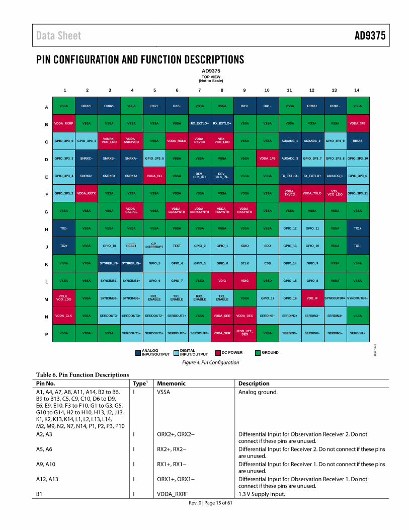
PIN CONFIGURATION AND FUNCTION DESCRIPTIONS
VSSA
VSSA VSSA VSSA VSSA
VSSA
VSSA
VSSA VSSA
VSSA VSSA
VSSA
VSSA VSSAVSSA
VSSA
VSSA VSSAVSSA
VSSA VSSA VSSA VSSA
VSSA VSSA VSSA
VSSA VSSA VSSA VSSA VSSA VSSA VSSA VSSA
VSSA VSSA VSSA VSSAVSSA
VSSAVSSA VSSA VSSA VSSA VSSA VSSA VSSA VSSA
VSSAVSSA
VSSA
VSSAVSSA
VSSA
VSSAVSSA
VSSAVSSA
VSSA
VSSA
VSSAVSSAVSSA
VSSA
VSSAVSSA
VSSAVSSA
VSSA
VSSD
VSSA
VSSD
VSSA
VSSA
ORX2+ ORX2– RX2+ RX2– RX1+ RX1– ORX1+ ORX1–
RX_EXTLO– RX_EXTLO+
AUXADC_1 AUXADC_2
AUXADC_3
RBIAS
AUXADC_0TX_EXTLO– TX_EXTLO+DEV_CLK_IN+
DEV_CLK_IN–SNRXA+
SNRXA–
SNRXB+
SNRXB–
SNRXC+
SNRXC–
TX2+
TX2–
TX1–
TX1+
SYSREF_IN+ SYSREF_IN–
VDDA_RXRF
VSNRX_VCO_LDO
VDDA_SNRXVCO VDDA_RXLO VRX_
VCO_LDOVDDA_RXVCO
VDDA_3P3
VDDA_1P8
VDDA_BB
VDDA_RXTX
VDDA_CALPLL
VDDA_CLKSYNTH
VDDA_SNRXSYNTH
VDDA_TXSYNTH
VDD_IF
VDDA_RXSYNTH
VDDA_TXVCO VDDA_TXLO VTX_
VCO_LDO
VDIGVDIG
VCLK_VCO_LDO
VDDA_CLK VDDA_SER
VDDA_SER
VDDA_DES
JESD_VTT_DES SERDIN1+SERDIN1–SERDIN0+SERDIN0–
SERDIN3+SERDIN3–SERDIN2+SERDIN2–
SERDOUT0+SERDOUT0–SERDOUT1+SERDOUT1–
SERDOUT2+SERDOUT2–SERDOUT3+SERDOUT3–
SYNCINB0+SYNCINB0–
SYNCINB1+SYNCINB1–
SYNCOUTB0–SYNCOUTB0+GPIO_17 GPIO_16
GPIO_15 GPIO_8
GPIO_9GPIO_14
GPIO_10
GPIO_11
GPIO_13
GPIO_12
GPIO_0
GPIO_1
GPIO_3
GPIO_2
GPIO_4
GPIO_7
GPIO_5
GPIO_6
SDIO
SCLK
SDO
CSB
GPIO_18 RESET GP_INTERRUPT TEST
RX1_ENABLE
TX1_ENABLE
RX2_ENABLE
TX2_ENABLE
GPIO_3P3_5
GPIO_3P3_0 GPIO_3P3_1
GPIO_3P3_3
GPIO_3P3_4
GPIO_3P3_2
GPIO_3P3_10
GPIO_3P3_6
GPIO_3P3_11
GPIO_3P3_9
GPIO_3P3_8GPIO_3P3_7
1 4 7 8 11 142 3 5 6 9 10 12 13
A
G
K
L
P
J
H
B
M
N
C
D
E
F
ANALOGINPUT/OUTPUT
DIGITALINPUT/OUTPUT DC POWER GROUND
AD9375TOP VIEW
(Not to Scale)
1565
7-00
4
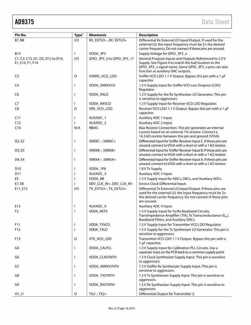
Figure 4. Pin Configuration
Table 6. Pin Function Descriptions Pin No. Type1 Mnemonic Description A1, A4, A7, A8, A11, A14, B2 to B6, B9 to B13, C5, C9, C10, D6 to D9, E6, E9, E10, F3 to F10, G1 to G3, G5, G10 to G14, H2 to H10, H13, J2, J13, K1, K2, K13, K14, L1, L2, L13, L14, M2, M9, N2, N7, N14, P1, P2, P3, P10
I VSSA Analog ground.
A2, A3 I ORX2+, ORX2− Differential Input for Observation Receiver 2. Do not connect if these pins are unused.
A5, A6 I RX2+, RX2− Differential Input for Receiver 2. Do not connect if these pins are unused.
A9, A10 I RX1+, RX1− Differential Input for Receiver 1. Do not connect if these pins are unused.
A12, A13 I ORX1+, ORX1− Differential Input for Observation Receiver 1. Do not connect if these pins are unused.
B1 I VDDA_RXRF 1.3 V Supply Input.
AD9375 Data Sheet
Rev. 0 | Page 16 of 61
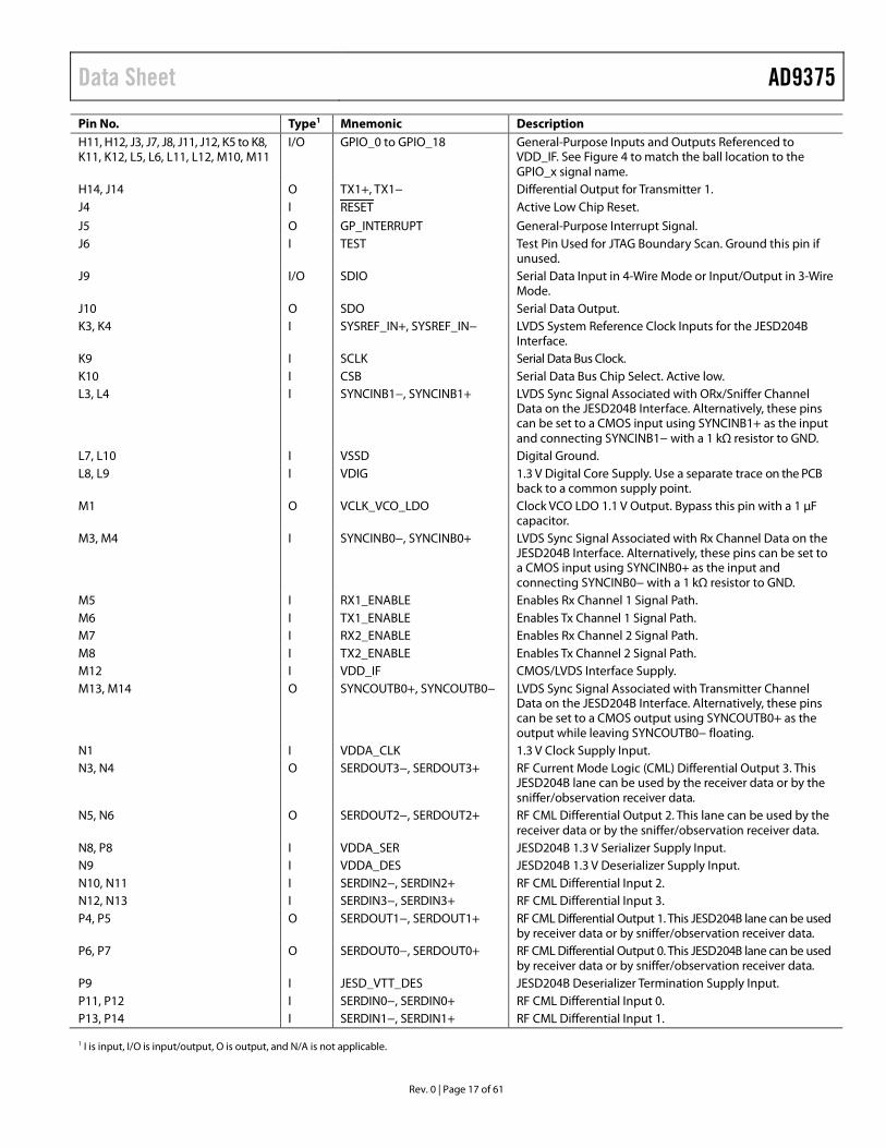
Pin No. Type1 Mnemonic Description B7, B8 I/O RX_EXTLO−, RX_EXTLO+ Differential Rx External LO Input/Output. If used for the
external LO, the input frequency must be 2× the desired carrier frequency. Do not connect if these pins are unused.
B14 I VDDA_3P3 Supply Voltage for GPIO_3P3_x. C1, C2, C13, D1, D5, D12 to D14, E1, E14, F1, F14
I/O GPIO_3P3_0 to GPIO_3P3_11 General-Purpose Inputs and Outputs Referenced to 3.3 V Supply. See Figure 4 to match the ball location to the GPIO_3P3_x signal name. Some GPIO_3P3_x pins can also function as auxiliary DAC outputs.
C3 O VSNRX_VCO_LDO Sniffer VCO LDO 1.1 V Output. Bypass this pin with a 1 µF capacitor.
C4 I VDDA_SNRXVCO 1.3 V Supply Input for Sniffer VCO Low Dropout (LDO) Regulator.
C6 I VDDA_RXLO 1.3 V Supply for the Rx Synthesizer LO Generator. This pin is sensitive to aggressors.
C7 I VDDA_RXVCO 1.3 V Supply Input for Receiver VCO LDO Regulator. C8 O VRX_VCO_LDO Receiver VCO LDO 1.1 V Output. Bypass this pin with a 1 µF
capacitor. C11 I AUXADC_1 Auxiliary ADC 1 Input. C12 I AUXADC_2 Auxiliary ADC 2 Input. C14 N/A RBIAS Bias Resistor Connection. This pin generates an internal
current based on an external 1% resistor. Connect a 14.3 kΩ resistor between this pin and ground (VSSA).
D2, E2 I SNRXC−, SNRXC+ Differential Input for Sniffer Receiver Input C. If these pins are unused, connect to VSSA with a short or with a 1 kΩ resistor.
D3, E3 I SNRXB−, SNRXB+ Differential Input for Sniffer Receiver Input B. If these pins are unused, connect to VSSA with a short or with a 1 kΩ resistor.
D4, E4 I SNRXA−, SNRXA+ Differential Input for Sniffer Receiver Input A. If these pins are unused, connect to VSSA with a short or with a 1 kΩ resistor.
D10 I VDDA_1P8 1.8 V Tx Supply. D11 I AUXADC_3 Auxiliary ADC 3 Input. E5 I VDDA_BB 1.3 V Supply Input for ADCs, DACs, and Auxiliary ADCs. E7, E8 I DEV_CLK_IN+, DEV_CLK_IN− Device Clock Differential Input. E11, E12 I/O TX_EXTLO−, TX_EXTLO+ Differential Tx External LO Input/Output. If these pins are
used for the external LO, the input frequency must be 2× the desired carrier frequency. Do not connect if these pins are unused.
E13 I AUXADC_0 Auxiliary ADC 0 Input. F2 I VDDA_RXTX 1.3 V Supply Input for Tx/Rx Baseband Circuits,
Transimpedance Amplifier (TIA), Tx Transconductance (Gm), Baseband Filters, and Auxiliary DACs.
F11 I VDDA_TXVCO 1.3 V Supply Input for Transmitter VCO LDO Regulator. F12 I VDDA_TXLO 1.3 V Supply for the Tx Synthesizer LO Generator. This pin is
sensitive to aggressors. F13 O VTX_VCO_LDO Transmitter VCO LDO 1.1 V Output. Bypass this pin with a
1 µF capacitor. G4 I VDDA_CALPLL 1.3 V Supply Input for Calibration PLL Circuits. Use a
separate trace on the PCB back to a common supply point. G6 I VDDA_CLKSYNTH 1.3 V Clock Synthesizer Supply Input. This pin is sensitive
to aggressors. G7 I VDDA_SNRXSYNTH 1.3 V Sniffer Rx Synthesizer Supply Input. This pin is
sensitive to aggressors. G8 I VDDA_TXSYNTH 1.3 V Tx Synthesizer Supply Input. This pin is sensitive to
aggressors. G9 I VDDA_RXSYNTH 1.3 V Rx Synthesizer Supply Input. This pin is sensitive to
aggressors. H1, J1 O TX2−, TX2+ Differential Output for Transmitter 2.
Data Sheet AD9375
Rev. 0 | Page 17 of 61
Pin No. Type1 Mnemonic Description H11, H12, J3, J7, J8, J11, J12, K5 to K8, K11, K12, L5, L6, L11, L12, M10, M11
I/O GPIO_0 to GPIO_18 General-Purpose Inputs and Outputs Referenced to VDD_IF. See Figure 4 to match the ball location to the GPIO_x signal name.
H14, J14 O TX1+, TX1− Differential Output for Transmitter 1. J4 I RESET Active Low Chip Reset.
J5 O GP_INTERRUPT General-Purpose Interrupt Signal. J6 I TEST Test Pin Used for JTAG Boundary Scan. Ground this pin if
unused. J9 I/O SDIO Serial Data Input in 4-Wire Mode or Input/Output in 3-Wire
Mode. J10 O SDO Serial Data Output. K3, K4 I SYSREF_IN+, SYSREF_IN− LVDS System Reference Clock Inputs for the JESD204B
Interface. K9 I SCLK Serial Data Bus Clock. K10 I CSB Serial Data Bus Chip Select. Active low. L3, L4 I SYNCINB1−, SYNCINB1+ LVDS Sync Signal Associated with ORx/Sniffer Channel
Data on the JESD204B Interface. Alternatively, these pins can be set to a CMOS input using SYNCINB1+ as the input and connecting SYNCINB1− with a 1 kΩ resistor to GND.
L7, L10 I VSSD Digital Ground. L8, L9 I VDIG 1.3 V Digital Core Supply. Use a separate trace on the PCB
back to a common supply point. M1 O VCLK_VCO_LDO Clock VCO LDO 1.1 V Output. Bypass this pin with a 1 µF
capacitor. M3, M4 I SYNCINB0−, SYNCINB0+ LVDS Sync Signal Associated with Rx Channel Data on the
JESD204B Interface. Alternatively, these pins can be set to a CMOS input using SYNCINB0+ as the input and connecting SYNCINB0− with a 1 kΩ resistor to GND.
M5 I RX1_ENABLE Enables Rx Channel 1 Signal Path. M6 I TX1_ENABLE Enables Tx Channel 1 Signal Path. M7 I RX2_ENABLE Enables Rx Channel 2 Signal Path. M8 I TX2_ENABLE Enables Tx Channel 2 Signal Path. M12 I VDD_IF CMOS/LVDS Interface Supply. M13, M14 O SYNCOUTB0+, SYNCOUTB0− LVDS Sync Signal Associated with Transmitter Channel
Data on the JESD204B Interface. Alternatively, these pins can be set to a CMOS output using SYNCOUTB0+ as the output while leaving SYNCOUTB0− floating.
N1 I VDDA_CLK 1.3 V Clock Supply Input. N3, N4 O SERDOUT3−, SERDOUT3+ RF Current Mode Logic (CML) Differential Output 3. This
JESD204B lane can be used by the receiver data or by the sniffer/observation receiver data.
N5, N6 O SERDOUT2−, SERDOUT2+ RF CML Differential Output 2. This lane can be used by the receiver data or by the sniffer/observation receiver data.
N8, P8 I VDDA_SER JESD204B 1.3 V Serializer Supply Input. N9 I VDDA_DES JESD204B 1.3 V Deserializer Supply Input. N10, N11 I SERDIN2−, SERDIN2+ RF CML Differential Input 2. N12, N13 I SERDIN3−, SERDIN3+ RF CML Differential Input 3. P4, P5 O SERDOUT1−, SERDOUT1+ RF CML Differential Output 1. This JESD204B lane can be used
by receiver data or by sniffer/observation receiver data. P6, P7 O SERDOUT0−, SERDOUT0+ RF CML Differential Output 0. This JESD204B lane can be used
by receiver data or by sniffer/observation receiver data. P9 I JESD_VTT_DES JESD204B Deserializer Termination Supply Input. P11, P12 I SERDIN0−, SERDIN0+ RF CML Differential Input 0. P13, P14 I SERDIN1−, SERDIN1+ RF CML Differential Input 1. 1 I is input, I/O is input/output, O is output, and N/A is not applicable.
AD9375 Data Sheet
Rev. 0 | Page 18 of 61
TYPICAL PERFORMANCE CHARACTERISTICS Temperature settings refer to the die temperature. The die temperature is 40°C for single-trace plots.
700 MHz BAND –30
–110
–100
–90
–80
–70
–60
–50
–40
300 400 500 600 700 800 900 1000
REC
EIVE
R L
O L
EAK
AG
E (d
Bm
)
RECEIVER LO FREQUENCY (MHz)
+110°C+40°C–40°C
1565
7-30
5
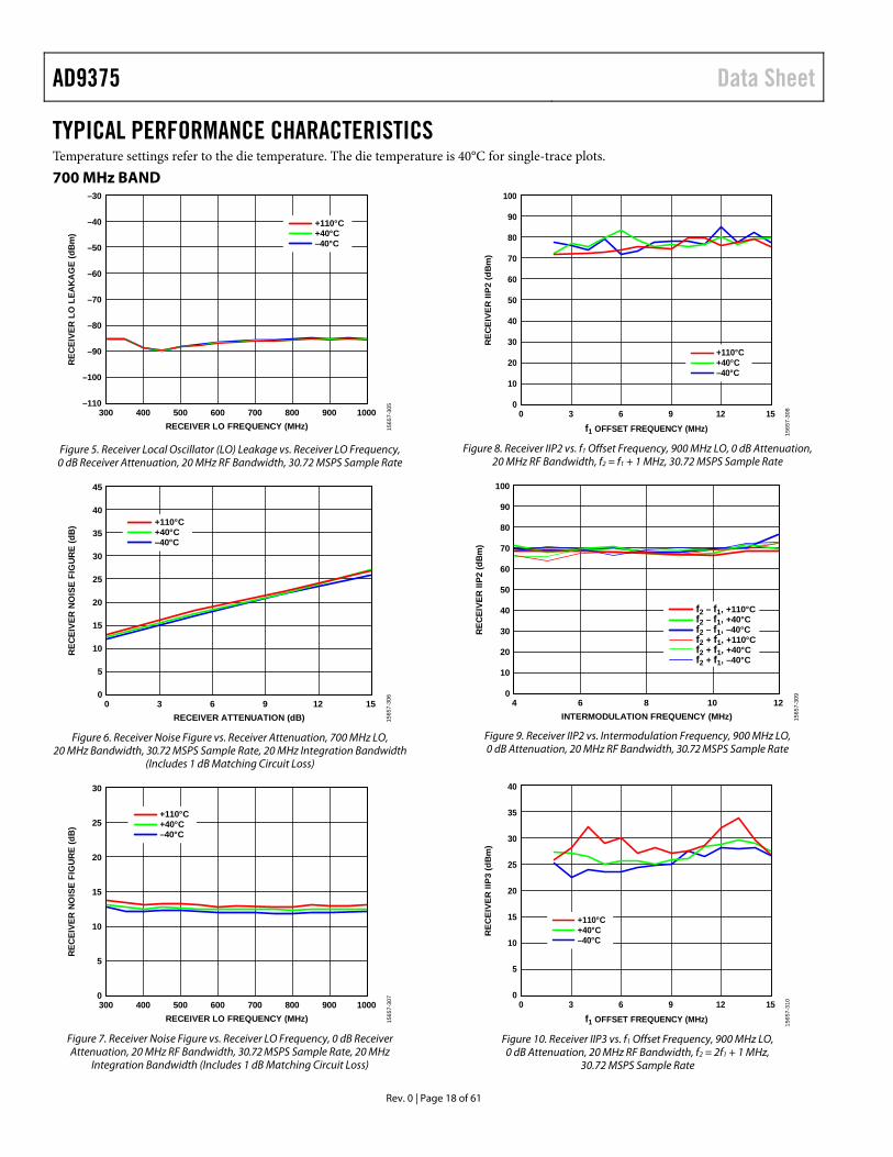
Figure 5. Receiver Local Oscillator (LO) Leakage vs. Receiver LO Frequency, 0 dB Receiver Attenuation, 20 MHz RF Bandwidth, 30.72 MSPS Sample Rate
45
0
5
10
15
20
25
30
35
40
0 3 6 9 12 15
REC
EIVE
R NO
ISE
FIG
URE
(dB
)
RECEIVER ATTENUATION (dB)
+110°C+40°C–40°C
1565
7-30
6
Figure 6. Receiver Noise Figure vs. Receiver Attenuation, 700 MHz LO, 20 MHz Bandwidth, 30.72 MSPS Sample Rate, 20 MHz Integration Bandwidth
(Includes 1 dB Matching Circuit Loss)
30
0
5
10
15
20
25
300 400 500 600 700 800 900 1000
REC
EIVE
R N
OIS
E FI
GU
RE
(dB
)
RECEIVER LO FREQUENCY (MHz)
+110°C+40°C–40°C
1565
7-30
7
Figure 7. Receiver Noise Figure vs. Receiver LO Frequency, 0 dB Receiver Attenuation, 20 MHz RF Bandwidth, 30.72 MSPS Sample Rate, 20 MHz
Integration Bandwidth (Includes 1 dB Matching Circuit Loss)
100
0
10
20
30
40
50
60
70
80
90
0 3 6 9 12 15
REC
EIV
ER
IIP
2 (d
Bm
)
f1 OFFSET FREQUENCY (MHz)
+110°C+40°C–40°C
1565
7-30
8
Figure 8. Receiver IIP2 vs. f1 Offset Frequency, 900 MHz LO, 0 dB Attenuation, 20 MHz RF Bandwidth, f2 = f1 + 1 MHz, 30.72 MSPS Sample Rate
100
0
10
20
30
40
50
60
70
80
90
4 6 8 10 12
REC
EIVE
R IIP
2 (d
Bm)
INTERMODULATION FREQUENCY (MHz)
f2 – f1, +110°Cf2 – f1, +40°Cf2 – f1, –40°Cf2 + f1, +110°Cf2 + f1, +40°Cf2 + f1, –40°C
1565
7-30
9
Figure 9. Receiver IIP2 vs. Intermodulation Frequency, 900 MHz LO, 0 dB Attenuation, 20 MHz RF Bandwidth, 30.72 MSPS Sample Rate
40
0
5
10
15
20
25
30
35
0 3 6 9 12 15
REC
EIV
ER
IIP
3 (d
Bm
)
f1 OFFSET FREQUENCY (MHz)
+110°C+40°C–40°C
1565
7-31
0
Figure 10. Receiver IIP3 vs. f1 Offset Frequency, 900 MHz LO, 0 dB Attenuation, 20 MHz RF Bandwidth, f2 = 2f1 + 1 MHz,
30.72 MSPS Sample Rate
Data Sheet AD9375
Rev. 0 | Page 19 of 61
40
0
5
10
15
20
25
30
35
4 6 8 10 12
REC
EIVE
R IIP
3 (d
Bm)
INTERMODULATION FREQUENCY (MHz)
f2 – 2f1, +110°Cf2 – 2f1, +40°Cf2 – 2f1, –40°Cf2 + 2f1, +110°Cf2 + 2f1, +40°Cf2 + 2f1, –40°C
1565
7-31
1
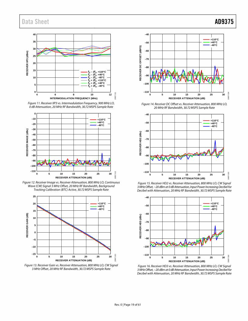
Figure 11. Receiver IIP3 vs. Intermodulation Frequency, 900 MHz LO, 0 dB Attenuation, 20 MHz RF Bandwidth, 30.72 MSPS Sample Rate
0
–110
–100
–90
–80
–70
–60
–50
–40
–20
–30
–10
0 5 10 15 20 25 30
REC
EIVE
R IM
AGE
(dB
c)
RECEIVER ATTENUATION (dB)
+110°C+40°C–40°C
1565
7-31
2
Figure 12. Receiver Image vs. Receiver Attenuation, 800 MHz LO, Continuous Wave (CW) Signal 3 MHz Offset, 20 MHz RF Bandwidth, Background
Tracking Calibration (BTC) Active, 30.72 MSPS Sample Rate
25
–15
–10
–5
0
5
15
10
20
0 5 10 15 20 25 30
REC
EIVE
R G
AIN
(dB)
RECEIVER ATTENUATION (dB)
+110°C+40°C–40°C
1565
7-31
3
Figure 13. Receiver Gain vs. Receiver Attenuation, 800 MHz LO, CW Signal 3 MHz Offset, 20 MHz RF Bandwidth, 30.72 MSPS Sample Rate
–40
–110
–100
–90
–80
–70
–60
–50
0 5 10 15 20 25 30
REC
EIVE
R D
C O
FFSE
T (d
BFS
)
RECEIVER ATTENUATION (dB)
+110°C+40°C–40°C
1565
7-31
4
Figure 14. Receiver DC Offset vs. Receiver Attenuation, 800 MHz LO, 20 MHz RF Bandwidth, 30.72 MSPS Sample Rate
–40
–110
–100
–90
–80
–70
–60
–50
0 5 10 15 20 25 30
REC
EIVE
R H
D2 (d
Bc)
RECEIVER ATTENUATION (dB)
+110°C+40°C–40°C
1565
7-31
5
Figure 15. Receiver HD2 vs. Receiver Attenuation, 800 MHz LO, CW Signal 3 MHz Offset, −20 dBm at 0 dB Attenuation, Input Power Increasing Decibel for Decibel with Attenuation, 20 MHz RF Bandwidth, 30.72 MSPS Sample Rate
–40
–110
–100
–90
–80
–70
–60
–50
0 5 10 15 20 25 30
REC
EIVE
R HD
3 (d
Bc)
RECEIVER ATTENUATION (dB)
+110°C+40°C–40°C
1565
7-31
6
Figure 16. Receiver HD3 vs. Receiver Attenuation, 800 MHz LO, CW Signal 3 MHz Offset, −20 dBm at 0 dB Attenuation, Input Power Increasing Decibel for Decibel with Attenuation, 20 MHz RF Bandwidth, 30.72 MSPS Sample Rate
AD9375 Data Sheet
Rev. 0 | Page 20 of 61
0
–60
–50
–40
–30
–20
–10
–60 –55 –50 –45 –40 –35 –30 –25 –20 –15 –10 –5 0
RECE
IVER
EVM
(dB)
RECEIVER INPUT POWER (dBm)
+110°C+40°C–40°C
1565
7-31
7
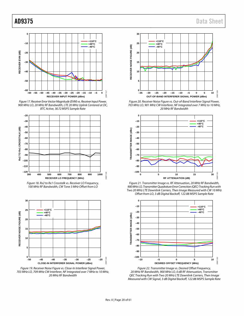
Figure 17. Receiver Error Vector Magnitude (EVM) vs. Receiver Input Power,
900 MHz LO, 20 MHz RF Bandwidth, LTE 20 MHz Uplink Centered at DC, BTC Active, 30.72 MSPS Sample Rate
–20
–120
–100
–80
–110
–90
–70
–60
–50
–40
–30
300 400 500 600 700 800 900 1000
Rx2
TO
Rx1
CR
OSS
TALK
(dB
)
RECEIVER LO FREQUENCY (MHz) 1565
7-31
8
Figure 18. Rx2 to Rx1 Crosstalk vs. Receiver LO Frequency, 100 MHz RF Bandwidth, CW Tone 3 MHz Offset from LO
30
0
5
10
15
20
25
–50 –45 –40 –35 –30 –25 –20
REC
EIVE
R N
OIS
E FI
GU
RE
(dB
)
CLOSE-IN INTERFERER SIGNAL POWER (dBm)
+110°C+40°C–40°C
1565
7-31
9
Figure 19. Receiver Noise Figure vs. Close-In Interferer Signal Power,
703 MHz LO, 709 MHz CW Interferer, NF Integrated over 7 MHz to 10 MHz, 20 MHz RF Bandwidth
30
0
5
10
15
20
25
–35 –30 –25 –20 –10 0–15 –5 5 10
RECE
IVER
NO
ISE
FIG
URE
(dB)
OUT-OF-BAND INTERFERER SIGNAL POWER (dBm)
+110°C+40°C–40°C
1565
7-32
0
Figure 20. Receiver Noise Figure vs. Out-of-Band Interferer Signal Power,
703 MHz LO, 901 MHz CW Interferer, NF Integrated over 7 MHz to 10 MHz, 20 MHz RF Bandwidth
0
–100
–90
–80
–70
–60
–50
–40
–20
–30
–10
0 5 10 15 30
TRAN
SMIT
TER
IMAG
E (d
Bc)
RF ATTENUATION (dB)
+110°C+40°C–40°C
1565
7-32
1
Figure 21. Transmitter Image vs. RF Attenuation, 20 MHz RF Bandwidth,
900 MHz LO, Transmitter Quadrature Error Correction (QEC) Tracking Run with Two 20 MHz LTE Downlink Carriers, Then Image Measured with CW 10 MHz
Offset from LO, 3 dB Digital Backoff, 122.88 MSPS Sample Rate
0
–100
–90
–80
–70
–60
–50
–40
–20
–30
–10
–10 –5 0 5 10
TRAN
SMIT
TER
IMAG
E (d
Bc)
DESIRED OFFSET FREQUENCY (MHz)
+110°C+40°C–40°C
1565
7-32
2
Figure 22. Transmitter Image vs. Desired Offset Frequency,
20 MHz RF Bandwidth, 900 MHz LO, 0 dB RF Attenuation, Transmitter QEC Tracking Run with Two 20 MHz LTE Downlink Carriers, Then Image
Measured with CW Signal, 3 dB Digital Backoff, 122.88 MSPS Sample Rate
Data Sheet AD9375
Rev. 0 | Page 21 of 61
10
–10
–8
–6
–4
–2
0
2
6
4
8
300 400 600 800500 700 900 1000
Tx O
UTP
UT
(dB
m)
FREQUENCY (MHz)
+110°C+40°C–40°C
1565
7-32
3
Figure 23. Tx Output Power, Transmitter QEC, and External LO Leakage
Tracking Active, 10 MHz CW Offset Signal, 1 MHz Resolution Bandwidth, 122.88 MSPS Sample Rate
–60
–100
–95
–90
–85
–80
–75
–70
–65
0 5 10 15 20
TRAN
SMIT
TER
LO L
EAKA
GE
(dBF
S)
RF ATTENUATION (dB)
+110°C+40°C–40°C
1565
7-32
4
Figure 24. Transmitter LO Leakage vs. RF Attenuation, 900 MHz LO, Transmitter
QEC and External LO Leakage Tracking Active, CW Signal 5 MHz Offset from LO, 6 dB Digital Backoff, 1 MHz Measurement Bandwidth (If Input Power to ORx Channel Is Not Held Constant, Performance Degrades As Shown in This Plot)
–60
–100
–95
–90
–85
–80
–75
–70
–65
–10 –5 0 5 10
TRAN
SMIT
TER
LO L
EAKA
GE
(dBF
S)
OFFSET FREQUENCY (MHz)
900MHz, +110°C900MHz, +40°C900MHz, –40°C600MHz, +110°C600MHz, +40°C600MHz, –40°C300MHz, +110°C300MHz, +40°C300MHz, –40°C
1565
7-32
5
Figure 25. Transmitter LO Leakage vs. Offset Frequency, Transmitter QEC and External LO Leakage Tracking Active,
5 dB Digital Backoff, 1 MHz Measurement Bandwidth
–20
–120
–100
–80
–110
–90
–70
–60
–50
–40
–30
300 400 500 600 700 800 900 1000
Tx1
TO R
x1 C
RO
SSTA
LK (d
B)
RECEIVER LO FREQUENCY (MHz) 1565
7-32
6
Figure 26. Tx1 to Rx1 Crosstalk vs. Receiver LO Frequency,
20 MHz Receiver RF Bandwidth, 20 MHz Transmitter RF Bandwidth, CW Signal 3 MHz Offset from LO
–20
–120
–100
–80
–110
–90
–70
–60
–50
–40
–30
300 400 500 600 700 800 900 1000
Tx2
TO R
x2 C
RO
SSTA
LK (d
B)
RECEIVER LO FREQUENCY (MHz) 1565
7-32
7
Figure 27. Tx2 to Rx2 Crosstalk vs. Receiver LO Frequency, 20 MHz Receiver RF Bandwidth, 20 MHz Transmitter RF Bandwidth, CW Signal 3 MHz Offset from LO
–20
–120
–100
–80
–110
–90
–70
–60
–50
–40
–30
300 400 500 600 700 800 900 1000
Tx2
TO T
x1 C
RO
SSTA
LK (d
B)
TRANSMITTER LO FREQUENCY (MHz) 1565
7-32
8
Figure 28. Tx2 to Tx1 Crosstalk vs. Transmitter LO Frequency, 20 MHz RF Bandwidth, CW Signal 3 MHz Offset from LO
AD9375 Data Sheet
Rev. 0 | Page 22 of 61
–80
–180
–160
–140
–170
–150
–130
–120
–110
–100
–90
0 5 10 15 20
TRAN
SMIT
TER
NOIS
E (d
Bm/H
z)
RF ATTENUATION (dB)
+110°C+40°C–40°C
1565
7-32
9
Figure 29. Transmitter Noise vs. RF Attenuation, 800 MHz LO,
20 MHz Offset Frequency
–40
–80
–75
0 4 8 12 16 20
Tx A
DJAC
ENT
CHAN
NEL
LEAK
AGE
RATI
O (d
Bc)
RF ATTENUATION (dB)
+110°C LOWER+40°C LOWER–40°C LOWER+110°C UPPER+40°C UPPER–40°C UPPER
–70
–65
–60
–55
–50
–45
1565
7-33
0
Figure 30. Tx Adjacent Channel Leakage Ratio vs. RF Attenuation, 900 MHz LO, 20 MHz RF Bandwidth, Four-Carrier W-CDMA Desired Signal, Transmitter
QEC and LO Leakage Tracking Active
–40
–80
–75
0 4 8 12 16 20
Tx A
LTER
NATE
CHA
NNEL
LEA
KAG
E RA
TIO
(dBc
)
RF ATTENUATION (dB)
+110°C LOWER+40°C LOWER–40°C LOWER+110°C UPPER+40°C UPPER–40°C UPPER
–70
–65
–60
–55
–50
–45
1565
7-33
1
Figure 31. Tx Alternate Channel Leakage Ratio vs. RF Attenuation,
900 MHz LO, 20 MHz RF Bandwidth, Four-Carrier W-CDMA Desired Signal, 2 dB Digital Backoff, Transmitter QEC and LO Leakage Tracking Active
–60
–150
–130
–140
100 1k 10k 100k 1M 10M
LO P
HA
SE N
OIS
E (d
Bc)
OFFSET FREQUENCY (Hz)
–120
–110
–100
–90
–80
–70
1565
7-33
2
Figure 32. LO Phase Noise vs. Offset Frequency, 3 dB Digital Backoff,
710 MHz LO
1.0
0
0.2
0.4
0.1
0.3
0.5
0.6
0.7
0.8
0.9
300 400 500 600 700 800 900 1000
Tx IN
TEG
RA
TED
PH
ASE
NO
ISE
(Deg
rees
)
TRANSMITTER LO FREQUENCY (MHz)
+110°C+40°C–40°C
1565
7-33
3
Figure 33. Tx Integrated Phase Noise vs. Transmitter LO Frequency, 20 MHz RF Bandwidth, CW 20 MHz Offset from LO, 3 dB Digital Backoff
35
0
5
10
15
20
25
30
0 6 12 184 10 162 8 14 20
TRAN
SMIT
TER
OIP
3 (d
Bm)
RF ATTENUATION (dB)
+110°C+40°C–40°C
1565
7-33
4
Figure 34. Transmitter OIP3 vs. RF Attenuation, 800 MHz LO,
20 MHz RF Bandwidth, f1 = 10 MHz, f2 = 11 MHz, 3 dB Digital Backoff, 122.88 MSPS Sample Rate
Data Sheet AD9375
Rev. 0 | Page 23 of 61
0
–100
–80
–60
–90
–70
–50
–40
–30
–20
–10
700 725 750 775 800 825 850 875 900
Tx O
UTP
UT
(dB
m)
FREQUENCY (MHz) 1565
7-33
5
Figure 35. Tx Output Power Spectrum, 2 dB Digital and 3 dB RF Backoff,
20 MHz RF Bandwidth, Transmitter QEC, and Internal LO Leakage Active, LTE 10 MHz Signal, 800 MHz LO, 1 MHz Resolution Bandwidth,
122.88 MSPS Sample Rate, Test Equipment Noise Floor De-Embedded
0
–100
–80
–60
–90
–70
–50
–40
–30
–20
–10
300 400 500 600 700 800 900 11001000 1200 1300
Tx O
UTP
UT
(dB
m)
FREQUENCY (MHz) 1565
7-33
6
Figure 36. Tx Output Power Spectrum, 2 dB Digital and 3 dB RF Backoff,
20 MHz RF Bandwidth, Transmitter QEC, and Internal LO Leakage Active, LTE 10 MHz Signal, 800 MHz LO, 1 MHz Resolution Bandwidth,
122.88 MSPS Sample Rate, Expanded Frequency View, Test Equipment Noise Floor De-Embedded
–20
–50
–45
–40
–35
–30
–25
0 4 8 12 16 20
TRAN
SMIT
TER
EVM
(dB)
RF ATTENUATION (dB)
+110°C+40°C–40°C
1565
7-33
7
Figure 37. Transmitter EVM vs. RF Attenuation, 900 MHz LO,
Transmitter LO Leakage and Transmitter QEC Tracking Active, 20 MHz RF Bandwidth, LTE 20 MHz Downlink Signal, 122.88 MSPS Sample Rate
0
–100
–80
–60
–90
–70
–50
–40
–30
–20
–10
0 5 10 15 20 25 30
TRAN
SMIT
TER
HD2
(dBc
)
RF ATTENUATION (dB)
+110°C+40°C–40°C
1565
7-33
8
Figure 38. Transmitter HD2 vs. RF Attenuation, 800 MHz LO,
810 MHz CW Desired Signal, 20 MHz RF Bandwidth, 122.88 MSPS Sample Rate
0
–80
–60
–70
–50
–40
–30
–20
–10
0 5 10 15 20
TRAN
SMIT
TER
HD3
(dBc
)
RF ATTENUATION (dB)
+110°C+40°C–40°C
1565
7-33
9
Figure 39. Transmitter HD3 vs. RF Attenuation, 800 MHz LO,
810 MHz CW Desired Signal, 20 MHz RF Bandwidth, 122.88 MSPS Sample Rate
10
–20
–15
–10
–5
0
5
0 5 10 15 20
TRAN
SMIT
TER
OUT
PUT
POW
ER (d
Bm)
RF ATTENUATION (dB)
+110°C+40°C–40°C
1565
7-34
0
Figure 40. Transmitter Output Power vs. RF Attenuation, 800 MHz LO,
810 MHz CW Desired Signal, 20 MHz RF Bandwidth, 122.88 MSPS Sample Rate
AD9375 Data Sheet
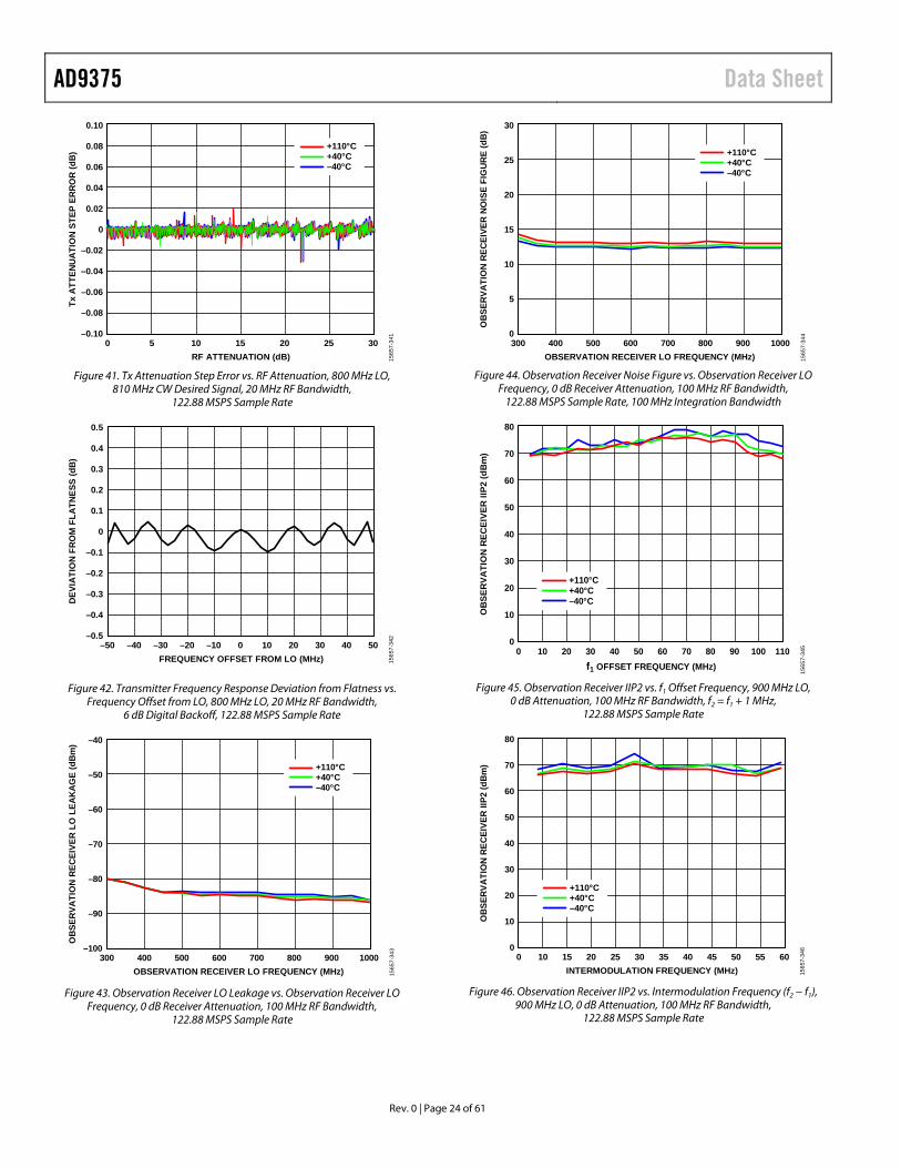
Rev. 0 | Page 24 of 61
0.10
–0.10
–0.06
–0.02
–0.08
–0.04
0
0.02
0.04
0.06
0.08
0 5 10 15 20 25 30
Tx A
TTEN
UATI
ON
STEP
ERR
OR
(dB)
RF ATTENUATION (dB)
+110°C+40°C–40°C
1565
7-34
1
Figure 41. Tx Attenuation Step Error vs. RF Attenuation, 800 MHz LO,
810 MHz CW Desired Signal, 20 MHz RF Bandwidth, 122.88 MSPS Sample Rate
0.5
–0.5
–0.3
–0.1
–0.4
–0.2
0
0.1
0.2
0.3
0.4
–50 –40 –20 0 20–30 –10 10 30 40 50
DEVI
ATIO
N FR
OM
FLA
TNES
S (d
B)
FREQUENCY OFFSET FROM LO (MHz) 1565
7-34
2
Figure 42. Transmitter Frequency Response Deviation from Flatness vs. Frequency Offset from LO, 800 MHz LO, 20 MHz RF Bandwidth,
6 dB Digital Backoff, 122.88 MSPS Sample Rate
–40
–100
–90
–80
–70
–60
–50
300 400 500 600 700 800 900 1000
OB
SER
VATI
ON
REC
EIVE
R L
O L
EAK
AG
E (d
Bm
)
OBSERVATION RECEIVER LO FREQUENCY (MHz)
+110°C+40°C–40°C
1565
7-34
3
Figure 43. Observation Receiver LO Leakage vs. Observation Receiver LO Frequency, 0 dB Receiver Attenuation, 100 MHz RF Bandwidth,
122.88 MSPS Sample Rate
30
0
5
10
15
20
25
300 400 500 600 700 800 900 1000
OB
SER
VATI
ON
REC
EIVE
R N
OIS
E FI
GU
RE
(dB
)
OBSERVATION RECEIVER LO FREQUENCY (MHz)
+110°C+40°C–40°C
1565
7-34
4
Figure 44. Observation Receiver Noise Figure vs. Observation Receiver LO
Frequency, 0 dB Receiver Attenuation, 100 MHz RF Bandwidth, 122.88 MSPS Sample Rate, 100 MHz Integration Bandwidth
80
0
10
20
30
40
50
60
70
0 30 60 90 10020 50 8010 40 70 110
OB
SER
VATI
ON
REC
EIVE
R II
P2 (d
Bm
)
f1 OFFSET FREQUENCY (MHz)
+110°C+40°C–40°C
1565
7-34
5
Figure 45. Observation Receiver IIP2 vs. f1 Offset Frequency, 900 MHz LO,
0 dB Attenuation, 100 MHz RF Bandwidth, f2 = f1 + 1 MHz, 122.88 MSPS Sample Rate
80
0
10
20
30
40
50
60
70
0 20 35 50 5515 30 4510 25 40 60
OBS
ERVA
TIO
N RE
CEIV
ER II
P2 (d
Bm)
INTERMODULATION FREQUENCY (MHz)
+110°C+40°C–40°C
1565
7-34
6
Figure 46. Observation Receiver IIP2 vs. Intermodulation Frequency (f2 − f1), 900 MHz LO, 0 dB Attenuation, 100 MHz RF Bandwidth,
122.88 MSPS Sample Rate
Data Sheet AD9375
Rev. 0 | Page 25 of 61
40
0
5
10
15
20
25
30
35
0 30 60 90 10020 50 8010 40 70 110
OB
SER
VATI
ON
REC
EIVE
R II
P3 (d
Bm
)
f1 OFFSET FREQUENCY (MHz)
+110°C+40°C–40°C
1565
7-34
7
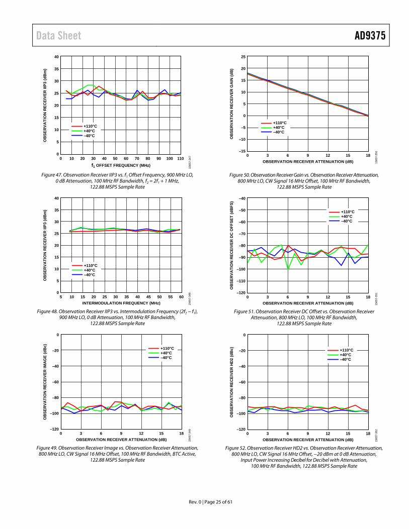
Figure 47. Observation Receiver IIP3 vs. f1 Offset Frequency, 900 MHz LO,
0 dB Attenuation, 100 MHz RF Bandwidth, f2 = 2f1 + 1 MHz, 122.88 MSPS Sample Rate
5 20 35 50 5515 30 4510 25 40 60INTERMODULATION FREQUENCY (MHz)
+110°C+40°C–40°C
40
0
5
10
15
20
25
30
35
OBS
ERVA
TIO
N RE
CEIV
ER II
P3 (d
Bm)
1565
7-34
8
Figure 48. Observation Receiver IIP3 vs. Intermodulation Frequency (2f2 − f1),
900 MHz LO, 0 dB Attenuation, 100 MHz RF Bandwidth, 122.88 MSPS Sample Rate
0
–120
–100
–80
–40
–60
–20
0 3 6 9 12 15 18
OBS
ERVA
TIO
N RE
CEIV
ER IM
AGE
(dBc
)
OBSERVATION RECEIVER ATTENUATION (dB)
+110°C+40°C–40°C
1565
7-34
9
Figure 49. Observation Receiver Image vs. Observation Receiver Attenuation,
800 MHz LO, CW Signal 16 MHz Offset, 100 MHz RF Bandwidth, BTC Active, 122.88 MSPS Sample Rate
25
–15
–10
–5
10
0
20
5
15
0 3 6 9 12 15 18
OBS
ERVA
TIO
N RE
CEIV
ER G
AIN
(dB)
OBSERVATION RECEIVER ATTENUATION (dB)
+110°C+40°C–40°C
1565
7-35
0
Figure 50. Observation Receiver Gain vs. Observation Receiver Attenuation, 800 MHz LO, CW Signal 16 MHz Offset, 100 MHz RF Bandwidth,
122.88 MSPS Sample Rate
–40
–120
–110
–100
–90
–80
–70
–60
–50
0 3 6 9 12 15 18
OBS
ERVA
TIO
N RE
CEIV
ER D
C O
FFSE
T (d
BFS)
OBSERVATION RECEIVER ATTENUATION (dB)
+110°C+40°C–40°C
1565
7-35
1
Figure 51. Observation Receiver DC Offset vs. Observation Receiver
Attenuation, 800 MHz LO, 100 MHz RF Bandwidth, 122.88 MSPS Sample Rate
0
–120
–100
–80
–60
–40
–20
0 3 6 9 12 15 18
OBS
ERVA
TIO
N RE
CEIV
ER H
D2 (d
Bc)
OBSERVATION RECEIVER ATTENUATION (dB)
+110°C+40°C–40°C
1565
7-35
2
Figure 52. Observation Receiver HD2 vs. Observation Receiver Attenuation,
800 MHz LO, CW Signal 16 MHz Offset, −20 dBm at 0 dB Attenuation, Input Power Increasing Decibel for Decibel with Attenuation,
100 MHz RF Bandwidth, 122.88 MSPS Sample Rate
AD9375 Data Sheet
Rev. 0 | Page 26 of 61
0
–100
–90
–80
–70
–60
–50
–40
–20
–30
–10
0 3 6 9 12 15 18
OBS
ERVA
TIO
N RE
CEIV
ER H
D3 (d
Bc)
OBSERVATION RECEIVER ATTENUATION (dB)
+110°C+40°C–40°C
1565
7-35
3
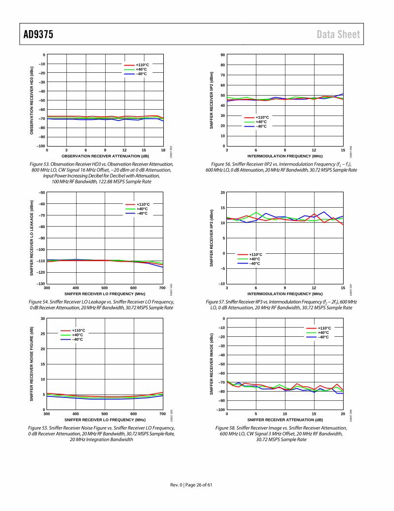
Figure 53. Observation Receiver HD3 vs. Observation Receiver Attenuation,
800 MHz LO, CW Signal 16 MHz Offset, −20 dBm at 0 dB Attenuation, Input Power Increasing Decibel for Decibel with Attenuation,
100 MHz RF Bandwidth, 122.88 MSPS Sample Rate
–50
–130
–120
–110
–100
–90
–70
–80
–60
300 400 500 600 700
SNIF
FER
REC
EIVE
R L
O L
EAK
AG
E (d
Bm
)
SNIFFER RECEIVER LO FREQUENCY (MHz)
+110°C+40°C–40°C
1565
7-35
4
Figure 54. Sniffer Receiver LO Leakage vs. Sniffer Receiver LO Frequency, 0 dB Receiver Attenuation, 20 MHz RF Bandwidth, 30.72 MSPS Sample Rate
300 400 500 600 700
30
0
5
10
20
15
25
SNIF
FER
REC
EIVE
R N
OIS
E FI
GU
RE
(dB
)
SNIFFER RECEIVER LO FREQUENCY (MHz)
+110°C+40°C–40°C
1565
7-35
5
Figure 55. Sniffer Receiver Noise Figure vs. Sniffer Receiver LO Frequency, 0 dB Receiver Attenuation, 20 MHz RF Bandwidth, 30.72 MSPS Sample Rate,
20 MHz Integration Bandwidth
90
0
10
20
50
30
70
60
40
80
3 6 9 12 15
SNIF
FER
RECE
IVER
IIP2
(dBm
)
INTERMODULATION FREQUENCY (MHz)
+110°C+40°C–40°C
1565
7-35
6
Figure 56. Sniffer Receiver IIP2 vs. Intermodulation Frequency (f2 − f1),
600 MHz LO, 0 dB Attenuation, 20 MHz RF Bandwidth, 30.72 MSPS Sample Rate
20
15
10
5
0
–5
–103 151296
SNIF
FER
RECE
IVER
IIP3
(dBm
)
INTERMODULATION FREQUENCY (MHz)
+110°C+40°C–40°C
1565
7-35
7
Figure 57. Sniffer Receiver IIP3 vs. Intermodulation Frequency (f2 − 2f1), 600 MHz
LO, 0 dB Attenuation, 20 MHz RF Bandwidth, 30.72 MSPS Sample Rate
0 5 10 15 20
SNIF
FER
RECE
IVER
IMAG
E (d
Bc)
SNIFFER RECEIVER ATTENUATION (dB)
+110°C+40°C–40°C
0
–100
–80
–60
–90
–70
–50
–40
–30
–20
–10
1565
7-35
8
Figure 58. Sniffer Receiver Image vs. Sniffer Receiver Attenuation,
600 MHz LO, CW Signal 3 MHz Offset, 20 MHz RF Bandwidth, 30.72 MSPS Sample Rate
Data Sheet AD9375
Rev. 0 | Page 27 of 61
0 5 10 15 20
SNIF
FER
RECE
IVER
DC
OFF
SET
(dBF
S)
SNIFFER RECEIVER ATTENUATION (dB)
+110°C+40°C–40°C
–40
–110
–100
–80
–60
–90
–70
–50
1565
7-35
9
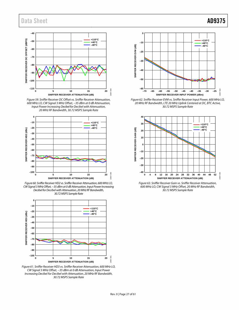
Figure 59. Sniffer Receiver DC Offset vs. Sniffer Receiver Attenuation, 600 MHz LO, CW Signal 3 MHz Offset, −35 dBm at 0 dB Attenuation,
Input Power Increasing Decibel for Decibel with Attenuation, 20 MHz RF Bandwidth, 30.72 MSPS Sample Rate
0 5 10 15 20
SNIF
FER
RECE
IVER
HD2
(dBc
)
SNIFFER RECEIVER ATTENUATION (dB)
+110°C+40°C–40°C
0
–100
–80
–60
–90
–70
–50
–40
–30
–20
–10
1565
7-36
0
Figure 60. Sniffer Receiver HD2 vs. Sniffer Receiver Attenuation, 600 MHz LO,
CW Signal 3 MHz Offset, −35 dBm at 0 dB Attenuation, Input Power Increasing Decibel for Decibel with Attenuation, 20 MHz RF Bandwidth,
30.72 MSPS Sample Rate
0 5 10 15 20
SNIF
FER
RECE
IVER
HD3
(dBc
)
SNIFFER RECEIVER ATTENUATION (dB)
+110°C+40°C–40°C
0
–100
–90
–80
–70
–60
–50
–40
–30
–20
–10
1565
7-36
1
Figure 61. Sniffer Receiver HD3 vs. Sniffer Receiver Attenuation, 600 MHz LO,
CW Signal 3 MHz Offset, −35 dBm at 0 dB Attenuation, Input Power Increasing Decibel for Decibel with Attenuation, 20 MHz RF Bandwidth,
30.72 MSPS Sample Rate
0
–60
–50
–40
–30
–20
–10
–70 –55 –50–65 –60 –45 –40 –35 –30 –25
SNIF
FER
REC
EIVE
R E
VM (d
B)
SNIFFER RECEIVER INPUT POWER (dBm)
+110°C+40°C–40°C
1565
7-36
2
Figure 62. Sniffer Receiver EVM vs. Sniffer Receiver Input Power, 600 MHz LO,
20 MHz RF Bandwidth, LTE 20 MHz Uplink Centered at DC, BTC Active, 30.72 MSPS Sample Rate
40
–40
–30
–20
–10
0
20
10
30
0 12 164 8 20 24 28 32 36 40 4844 52
SNIF
FER
RECE
IVER
GAI
N (d
B)
SNIFFER RECEIVER ATTENUATION (dB)
+110°C+40°C–40°C
1565
7-36
3
Figure 63. Sniffer Receiver Gain vs. Sniffer Receiver Attenuation,
600 MHz LO, CW Signal 3 MHz Offset, 20 MHz RF Bandwidth, 30.72 MSPS Sample Rate
AD9375 Data Sheet
Rev. 0 | Page 28 of 61
2.6 GHz BAND –30
–40
–50
–60
–70
–80
–90
–100
–110
1800
1900
2000
2100
2200
2300
2400
2500
2600
2700
2800
2900
REC
EIVE
R L
O L
EAK
AG
E (d
Bm
)
RECEIVER LO FREQUENCY (MHz)
+110°C+40°C–40°C
1565
7-00
5
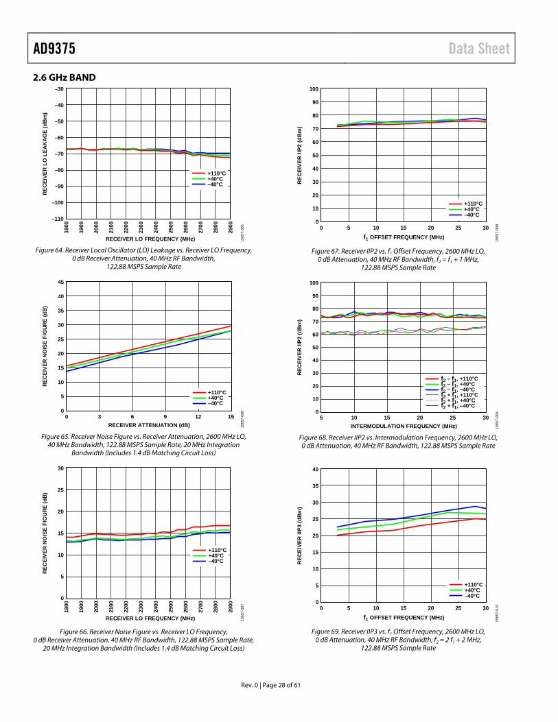
Figure 64. Receiver Local Oscillator (LO) Leakage vs. Receiver LO Frequency, 0 dB Receiver Attenuation, 40 MHz RF Bandwidth,
122.88 MSPS Sample Rate
45
0
10
5
15
20
25
30
35
40
RECE
IVER
NO
ISE
FIG
URE
(dB)
0 3 6 9 12 15RECEIVER ATTENUATION (dB)
+110°C+40°C–40°C
1565
7-00
6
Figure 65. Receiver Noise Figure vs. Receiver Attenuation, 2600 MHz LO,
40 MHz Bandwidth, 122.88 MSPS Sample Rate, 20 MHz Integration Bandwidth (Includes 1.4 dB Matching Circuit Loss)
30
0
5
10
15
20
25
1800
1900
2000
2100
2200
2300
2400
2500
2600
2700
2800
2900
REC
EIVE
R N
OIS
E FI
GU
RE
(dB
)
RECEIVER LO FREQUENCY (MHz)
+110°C+40°C–40°C
1565
7-00
7
Figure 66. Receiver Noise Figure vs. Receiver LO Frequency, 0 dB Receiver Attenuation, 40 MHz RF Bandwidth, 122.88 MSPS Sample Rate,
20 MHz Integration Bandwidth (Includes 1.4 dB Matching Circuit Loss)
100
0
30
20
10
40
50
60
70
80
90
REC
EIVE
R II
P2 (d
Bm
)
0 5 10 15 20 25 30f1 OFFSET FREQUENCY (MHz)
+110°C+40°C–40°C
1565
7-00
8
Figure 67. Receiver IIP2 vs. f1 Offset Frequency, 2600 MHz LO,
0 dB Attenuation, 40 MHz RF Bandwidth, f2 = f1 + 1 MHz, 122.88 MSPS Sample Rate
100
0
30
20
10
40
50
60
70
80
90RE
CEIV
ER II
P2 (d
Bm)
f2 – f1, +110°Cf2 – f1, +40°Cf2 – f1, –40°Cf2 + f1, +110°Cf2 + f1, +40°Cf2 + f1, –40°C
5 10 15 20 25 30INTERMODULATION FREQUENCY (MHz) 15
657-
009
Figure 68. Receiver IIP2 vs. Intermodulation Frequency, 2600 MHz LO, 0 dB Attenuation, 40 MHz RF Bandwidth, 122.88 MSPS Sample Rate
40
0
15
10
5
20
25
30
35
REC
EIVE
R II
P3 (d
Bm
)
0 5 10 15 20 25 30f1 OFFSET FREQUENCY (MHz)
+110°C+40°C–40°C
1565
7-01
0
Figure 69. Receiver IIP3 vs. f1 Offset Frequency, 2600 MHz LO,
0 dB Attenuation, 40 MHz RF Bandwidth, f2 = 2 f1 + 2 MHz, 122.88 MSPS Sample Rate
Data Sheet AD9375
Rev. 0 | Page 29 of 61
40
0
15
10
5
20
25
30
35
RECE
IVER
IIP3
(dBm
)
5 10 15 20 25 30INTERMODULATION FREQUENCY (MHz)
f2 – 2f1, +110°Cf2 – 2f1, +40°Cf2 – 2f1, –40°Cf2 + 2f1, +110°Cf2 + 2f1, +40°Cf2 + 2f1, –40°C
1565
7-01
1
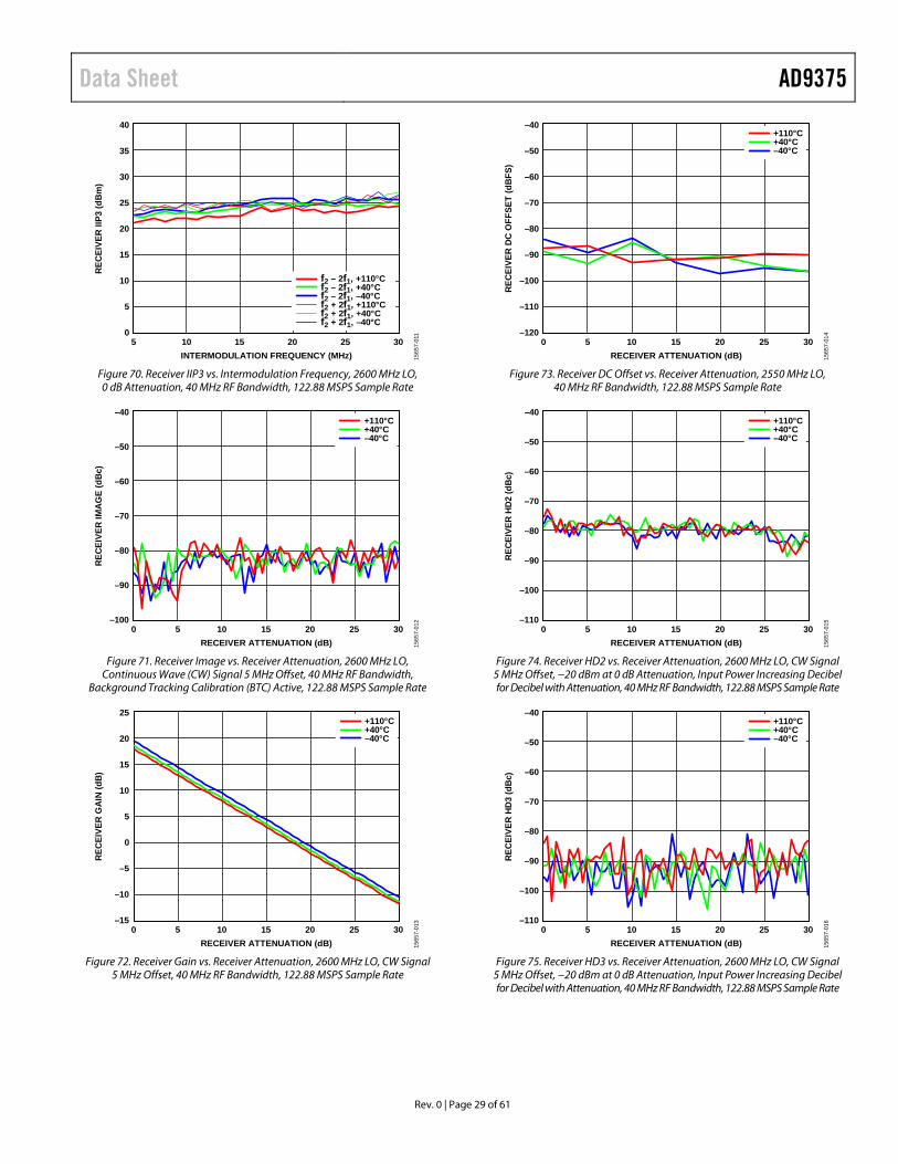
Figure 70. Receiver IIP3 vs. Intermodulation Frequency, 2600 MHz LO, 0 dB Attenuation, 40 MHz RF Bandwidth, 122.88 MSPS Sample Rate
–40
–100
–90
–80
–70
–60
–50
RECE
IVER
IMAG
E (d
Bc)
0 5 10 15 20 25 30RECEIVER ATTENUATION (dB)
+110°C+40°C–40°C
1565
7-01
2
Figure 71. Receiver Image vs. Receiver Attenuation, 2600 MHz LO,
Continuous Wave (CW) Signal 5 MHz Offset, 40 MHz RF Bandwidth, Background Tracking Calibration (BTC) Active, 122.88 MSPS Sample Rate
25
–15
–10
0
10
20
–5
5
15
RECE
IVER
GAI
N (d
B)
0 5 10 15 20 25 30RECEIVER ATTENUATION (dB)
+110°C+40°C–40°C
1565
7-01
3
Figure 72. Receiver Gain vs. Receiver Attenuation, 2600 MHz LO, CW Signal
5 MHz Offset, 40 MHz RF Bandwidth, 122.88 MSPS Sample Rate
–40
–120
–80
–60
–90
–100
–110
–70
–50
RECE
IVER
DC
OFF
SET
(dBF
S)
0 5 10 15 20 25 30RECEIVER ATTENUATION (dB)
+110°C+40°C–40°C
1565
7-01
4
Figure 73. Receiver DC Offset vs. Receiver Attenuation, 2550 MHz LO,
40 MHz RF Bandwidth, 122.88 MSPS Sample Rate
–40
–110
–100
–80
–60
–90
–70
–50
RECE
IVER
HD2
(dBc
)
0 5 10 15 20 25 30RECEIVER ATTENUATION (dB)
+110°C+40°C–40°C
1565
7-01
5
Figure 74. Receiver HD2 vs. Receiver Attenuation, 2600 MHz LO, CW Signal
5 MHz Offset, −20 dBm at 0 dB Attenuation, Input Power Increasing Decibel for Decibel with Attenuation, 40 MHz RF Bandwidth, 122.88 MSPS Sample Rate
–40
–110
–100
–80
–60
–90
–70
–50
RECE
IVER
HD3
(dBc
)
0 5 10 15 20 25 30RECEIVER ATTENUATION (dB)
+110°C+40°C–40°C
1565
7-01
6
Figure 75. Receiver HD3 vs. Receiver Attenuation, 2600 MHz LO, CW Signal
5 MHz Offset, −20 dBm at 0 dB Attenuation, Input Power Increasing Decibel for Decibel with Attenuation, 40 MHz RF Bandwidth, 122.88 MSPS Sample Rate
AD9375 Data Sheet
Rev. 0 | Page 30 of 61
0
–45
–35
–20
–10
–25
–40
–30
–15
–5
REC
EIVE
R E
VM (d
B)
–60 –50 –40 –30 –20 –10 0–55 –45 –35 –25 –15 –5RECEIVER INPUT POWER (dBm)
+110°C+40°C–40°C
1565
7-01
7
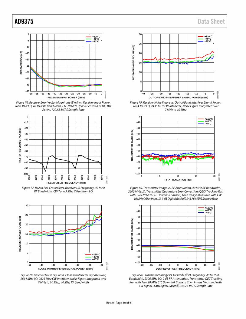
Figure 76. Receiver Error Vector Magnitude (EVM) vs. Receiver Input Power,
2600 MHz LO, 40 MHz RF Bandwidth, LTE 20 MHz Uplink Centered at DC, BTC Active, 122.88 MSPS Sample Rate
0
–20
–10
–30
–100
–90
–80
–70
–60
–50
–40
1800
1900
2000
2100
2200
2300
2400
2500
2600
2700
2800
2900
Rx2
TO
Rx1
CR
OSS
TALK
(dB
)
RECEIVER LO FREQUENCY (MHz) 1565
7-01
8
Figure 77. Rx2 to Rx1 Crosstalk vs. Receiver LO Frequency, 40 MHz
RF Bandwidth, CW Tone 3 MHz Offset from LO
30
0
5
10
15
20
25
REC
EIVE
R N
OIS
E FI
GU
RE
(dB
)
–50 –45 –40 –35 –30 –25 –20CLOSE-IN INTERFERER SIGNAL POWER (dBm)
+110°C+40°C–40°C
1565
7-01
9
Figure 78. Receiver Noise Figure vs. Close-In Interferer Signal Power, 2614 MHz LO, 2625 MHz CW Interferer, Noise Figure Integrated over
7 MHz to 10 MHz, 40 MHz RF Bandwidth
30
0
5
10
15
20
25
REC
EIVE
R N
OIS
E FI
GU
RE
(dB
)
–40 –35 –30 –25 –20 –15 –10 –5 0OUT-OF-BAND INTERFERER SIGNAL POWER (dBm)
+110°C+40°C–40°C
1565
7-02
0
Figure 79. Receiver Noise Figure vs. Out-of-Band Interferer Signal Power,
2614 MHz LO, 2435 MHz CW Interferer, Noise Figure Integrated over 7 MHz to 10 MHz
0
–20
–10
–30
–100
–90
–80
–70
–60
–50
–40
TRAN
SMIT
TER
IMAG
E (d
Bc)
0 15105 20RF ATTENUATION (dB)
+110°C+40°C–40°C
1565
7-02
1
Figure 80. Transmitter Image vs. RF Attenuation, 40 MHz RF Bandwidth, 2600 MHz LO, Transmitter Quadrature Error Correction (QEC) Tracking Run
with Two 20 MHz LTE Downlink Carriers, Then Image Measured with CW 10 MHz Offset from LO, 3 dB Digital Backoff, 245.76 MSPS Sample Rate
0
–20
–10
–30
–100
–90
–80
–70
–60
–50
–40
TRAN
SMIT
TER
IMAG
E (d
Bc)
–20 100–10 205–5–15 15DESIRED OFFSET FREQUENCY (MHz)
+110°C+40°C–40°C
1565
7-02
2
Figure 81. Transmitter Image vs. Desired Offset Frequency, 40 MHz RF Bandwidth, 2300 MHz LO, 0 dB RF Attenuation, Transmitter QEC Tracking Run with Two 20 MHz LTE Downlink Carriers, Then Image Measured with
CW Signal, 3 dB Digital Backoff, 245.76 MSPS Sample Rate
Data Sheet AD9375
Rev. 0 | Page 31 of 61
10
6
8
4
–10
–8
–6
–4
–2
0
2
1800
1900
2000
2100
2200
2300
2400
2500
2600
2700
2800
2900
Tx O
UTP
UT
(dB
m)
FREQUENCY (MHz)
+110°C+40°C–40°C
1565
7-02
3
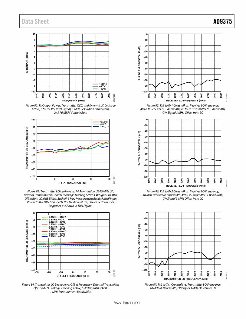
Figure 82. Tx Output Power, Transmitter QEC, and External LO Leakage
Active, 5 MHz CW Offset Signal, 1 MHz Resolution Bandwidth, 245.76 MSPS Sample Rate
–60
–100
–95
–85
–80
–70
–90
–75
–65
TRAN
SMIT
TER
LO L
EAKA
GE
(dBF
S)
0 5 10 15 20RF ATTENUATION (dB)
+110°C+40°C–40°C
1565
7-02
4
Figure 83. Transmitter LO Leakage vs. RF Attenuation, 2300 MHz LO, External Transmitter QEC and LO Leakage Tracking Active, CW Signal 10 MHz Offset from LO, 6 dB Digital Backoff, 1 MHz Measurement Bandwidth (If Input
Power to the ORx Channel Is Not Held Constant, Device Performance Degrades as Shown in This Figure)
–60
–100
–95
–85
–80
–70
–90
–75
–65
TRAN
SMIT
TER
LO L
EAKA
GE
(dBF
S)
1.8GHz, +110°C1.8GHz, +40°C1.8GHz, –40°C2.3GHz, +110°C2.3GHz, +40°C2.3GHz, –40°C2.8GHz, +110°C2.8GHz, +40°C2.8GHz, –40°C
–30 –10 10–20 0 20 30OFFSET FREQUENCY (MHz) 15
657-
025
Figure 84. Transmitter LO Leakage vs. Offset Frequency, External Transmitter QEC and LO Leakage Tracking Active, 6 dB Digital Backoff,
1 MHz Measurement Bandwidth
0
–20
–10
–30
–100
–90
–80
–70
–60
–50
–40
1800
1900
2000
2100
2200
2300
2400
2500
2600
2700
2800
2900
Tx1
TO R
x1 C
RO
SSTA
LK (d
B)
RECEIVER LO FREQUENCY (MHz) 1565
7-02
6
Figure 85. Tx1 to Rx1 Crosstalk vs. Receiver LO Frequency,
40 MHz Receiver RF Bandwidth, 40 MHz Transmitter RF Bandwidth, CW Signal 3 MHz Offset from LO
0
–20
–10
–30
–100
–90
–80
–70
–60
–50
–40
1800
1900
2000
2100
2200
2300
2400
2500
2600
2700
2800
2900
Tx2
TO R
x2 C
RO
SSTA
LK (d
B)
RECEIVER LO FREQUENCY (MHz) 1565
7-02
7
Figure 86. Tx2 to Rx2 Crosstalk vs. Receiver LO Frequency, 40 MHz Receiver RF Bandwidth, 40 MHz Transmitter RF Bandwidth,
CW Signal 3 MHz Offset from LO
0
–20
–10
–30
–100
–90
–80
–70
–60
–50
–40
1800
1900
2000
2100
2200
2300
2400
2500
2600
2700
2800
2900
Tx2
TO T
x1 C
RO
SSTA
LK (d
B)
TRANSMITTER LO FREQUENCY (MHz) 1565
7-02
8
Figure 87. Tx2 to Tx1 Crosstalk vs. Transmitter LO Frequency, 40 MHz RF Bandwidth, CW Signal 3 MHz Offset from LO
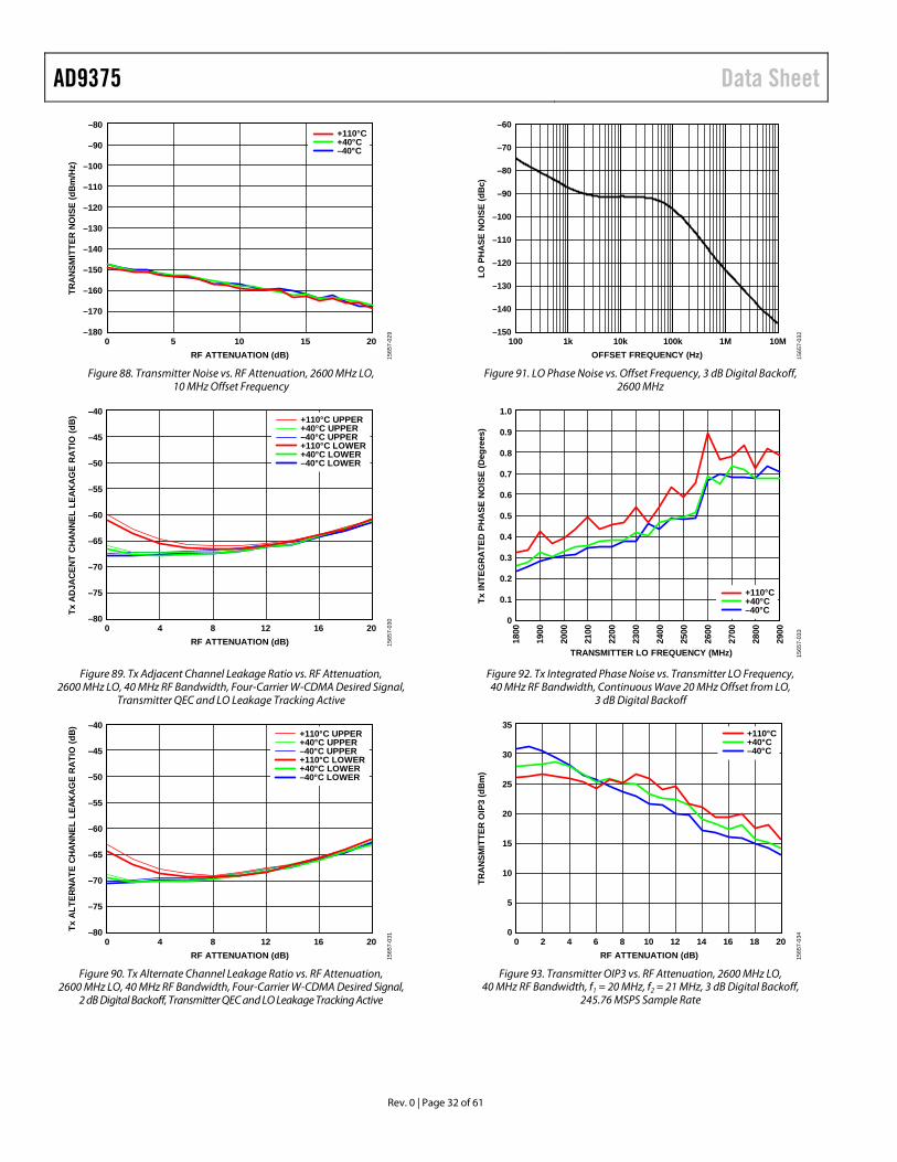
AD9375 Data Sheet
Rev. 0 | Page 32 of 61
–80
–180
–160
–130
–120
–100
–140
–170
–150
–110
–90
TRAN
SMIT
TER
NOIS
E (d
Bm/H
z)
0 5 10 15 20RF ATTENUATION (dB)
+110°C+40°C–40°C
1565
7-02
9
Figure 88. Transmitter Noise vs. RF Attenuation, 2600 MHz LO,
10 MHz Offset Frequency
–40
–80
–65
–70
–75
–60
–55
–50
–45
Tx A
DJAC
ENT
CHAN
NEL
LEAK
AGE
RATI
O (d
B)
0 4 8 12 16 20RF ATTENUATION (dB)
+110°C UPPER+40°C UPPER–40°C UPPER+110°C LOWER+40°C LOWER–40°C LOWER
1565
7-03
0
Figure 89. Tx Adjacent Channel Leakage Ratio vs. RF Attenuation, 2600 MHz LO, 40 MHz RF Bandwidth, Four-Carrier W-CDMA Desired Signal,
Transmitter QEC and LO Leakage Tracking Active
–40
–80
–65
–70
–75
–60
–55
–50
–45
Tx A
LTER
NATE
CHA
NNEL
LEA
KAG
E RA
TIO
(dB)
0 4 8 12 16 20RF ATTENUATION (dB)
+110°C UPPER+40°C UPPER–40°C UPPER+110°C LOWER+40°C LOWER–40°C LOWER
1565
7-03
1
Figure 90. Tx Alternate Channel Leakage Ratio vs. RF Attenuation,
2600 MHz LO, 40 MHz RF Bandwidth, Four-Carrier W-CDMA Desired Signal, 2 dB Digital Backoff, Transmitter QEC and LO Leakage Tracking Active
LO P
HA
SE N
OIS
E (d
Bc)
OFFSET FREQUENCY (Hz)
–150
–140
–130
–120
–110
–100
–90
–80
–70
–60
100 1k 10k 100k 1M 10M
1565
7-03
2
Figure 91. LO Phase Noise vs. Offset Frequency, 3 dB Digital Backoff,
2600 MHz
1.0
0
0.2
0.3
0.1
0.4
0.5
0.6
0.7
0.8
0.9
1800
1900
2000
2100
2200
2300
2400
2500
2600
2700
2800
2900
Tx IN
TEG
RA
TED
PH
ASE
NO
ISE
(Deg
rees
)
TRANSMITTER LO FREQUENCY (MHz)
+110°C+40°C–40°C
1565
7-03
3
Figure 92. Tx Integrated Phase Noise vs. Transmitter LO Frequency, 40 MHz RF Bandwidth, Continuous Wave 20 MHz Offset from LO,
3 dB Digital Backoff
35
0
5
10
15
20
25
30
TRAN
SMIT
TER
OIP
3 (d
Bm)
0 4 8 12 16 202 6 10 14 18RF ATTENUATION (dB)
+110°C+40°C–40°C
1565
7-03
4
Figure 93. Transmitter OIP3 vs. RF Attenuation, 2600 MHz LO,
40 MHz RF Bandwidth, f1 = 20 MHz, f2 = 21 MHz, 3 dB Digital Backoff, 245.76 MSPS Sample Rate
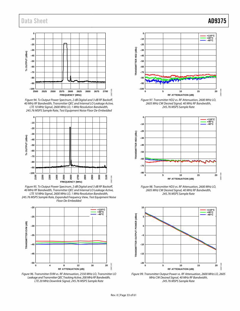
Data Sheet AD9375
Rev. 0 | Page 33 of 61
0
–100
–90
–80
–70
–50
–30
–10
–60
–40
–20
Tx O
UTP
UT
(dB
m)
2500 2550 2600 2650 27002525 2575 2625 2675FREQUENCY (MHz) 15
657-
035
Figure 94. Tx Output Power Spectrum, 2 dB Digital and 3 dB RF Backoff,
40 MHz RF Bandwidth, Transmitter QEC and Internal LO Leakage Active, LTE 10 MHz Signal, 2600 MHz LO, 1 MHz Resolution Bandwidth,
245.76 MSPS Sample Rate, Test Equipment Noise Floor De-Embedded
0
–100
–90
–80
–70
–50
–30
–10
–60
–40
–20
Tx O
UTP
UT
(dB
m)
2100
2300
2500
2800
3100
2200
2400
2600
3000
2750
2900
FREQUENCY (MHz) 1565
7-03
6
Figure 95. Tx Output Power Spectrum, 2 dB Digital and 3 dB RF Backoff,
40 MHz RF Bandwidth, Transmitter QEC and Internal LO Leakage Active, LTE 10 MHz Signal, 2600 MHz LO, 1 MHz Resolution Bandwidth,
245.76 MSPS Sample Rate, Expanded Frequency View, Test Equipment Noise Floor De-Embedded
–20
–50
–45
–40
–35
–30
–25
TRAN
SMIT
TER
EVM
(dB)
0 4 8 12 16 20RF ATTENUATION (dB)
+110°C+40°C–40°C
1565
7-03
7
Figure 96. Transmitter EVM vs. RF Attenuation, 2550 MHz LO, Transmitter LO
Leakage and Transmitter QEC Tracking Active, 200 MHz RF Bandwidth, LTE 20 MHz Downlink Signal, 245.76 MSPS Sample Rate
0
–20
–10
–30
–100
–90
–80
–70
–60
–50
–40
TRAN
SMIT
TER
HD2
(dBc
)
0 5 201510RF ATTENUATION (dB)
+110°C+40°C–40°C
1565
7-03
8
Figure 97. Transmitter HD2 vs. RF Attenuation, 2600 MHz LO,
2605 MHz CW Desired Signal, 40 MHz RF Bandwidth, 245.76 MSPS Sample Rate
0
–20
–10
–30
–80
–70
–60
–50
–40
TRAN
SMIT
TER
HD3
(dBc
)
0 20105 15RF ATTENUATION (dB)
+110°C+40°C–40°C
1565
7-03
9
Figure 98. Transmitter HD3 vs. RF Attenuation, 2600 MHz LO, 2605 MHz CW Desired Signal, 40 MHz RF Bandwidth,
245.76 MSPS Sample Rate
10
0
5
–5
–20
–15
–10
TRAN
SMIT
TER
OUT
PUT
POW
ER (d
Bm)
0 20105 15RF ATTENUATION (dB)
+110°C+40°C–40°C
1565
7-04
0
Figure 99. Transmitter Output Power vs. RF Attenuation, 2600 MHz LO, 2605
MHz CW Desired Signal, 40 MHz RF Bandwidth, 245.76 MSPS Sample Rate
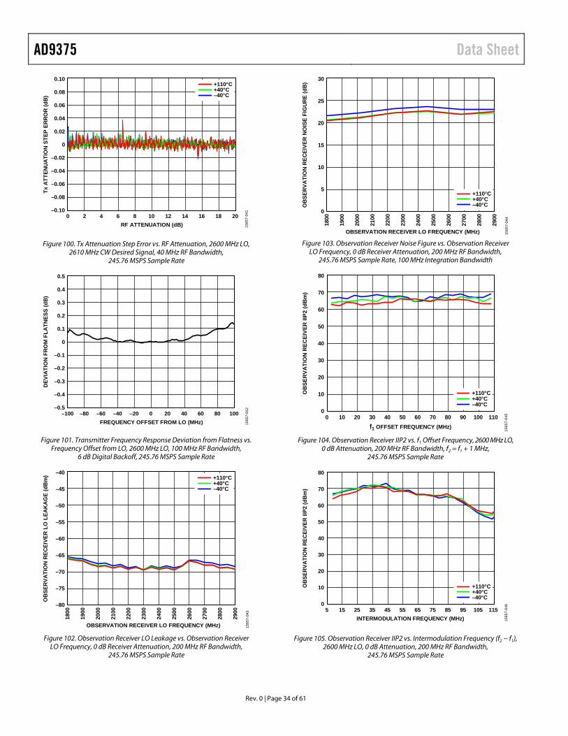
AD9375 Data Sheet
Rev. 0 | Page 34 of 61
0.10
0.04
0.08
0
–0.10
–0.08
–0.04
0.02
0.06
–0.02
–0.06
Tx A
TTEN
UATI
ON
STEP
ERR
OR
(dB)
0 201684 12 181462 10RF ATTENUATION (dB)
+110°C+40°C–40°C
1565
7-04
1
Figure 100. Tx Attenuation Step Error vs. RF Attenuation, 2600 MHz LO, 2610 MHz CW Desired Signal, 40 MHz RF Bandwidth,
245.76 MSPS Sample Rate
0.5
–0.5
–0.4
–0.3
–0.2
0
0.2
0.4
–0.1
0.1
0.3
DEV
IATI
ON
FR
OM
FLA
TNES
S (d
B)
–100 –60 –20 40 100–80 –40 0 8020 60FREQUENCY OFFSET FROM LO (MHz) 15
657-
042
Figure 101. Transmitter Frequency Response Deviation from Flatness vs. Frequency Offset from LO, 2600 MHz LO, 100 MHz RF Bandwidth,
6 dB Digital Backoff, 245.76 MSPS Sample Rate
–40
–80
–75
–65
–60
–70
–50
–45
–55
OB
SER
VATI
ON
REC
EIVE
R L
O L
EAK
AG
E (d
Bm
)
1800
1900
2000
2100
2200
2300
2400
2500
2600
2700
2800
2900
OBSERVATION RECEIVER LO FREQUENCY (MHz)
+110°C+40°C–40°C
1565
7-04
3
Figure 102. Observation Receiver LO Leakage vs. Observation Receiver LO Frequency, 0 dB Receiver Attenuation, 200 MHz RF Bandwidth,
245.76 MSPS Sample Rate
30
0
5
10
20
25
15
OB
SER
VATI
ON
REC
EIVE
R N
OIS
E FI
GU
RE
(dB
)
1800
1900
2000
2100
2200
2300
2400
2500
2600
2700
2800
2900
OBSERVATION RECEIVER LO FREQUENCY (MHz)
+110°C+40°C–40°C
1565
7-04
4
Figure 103. Observation Receiver Noise Figure vs. Observation Receiver
LO Frequency, 0 dB Receiver Attenuation, 200 MHz RF Bandwidth, 245.76 MSPS Sample Rate, 100 MHz Integration Bandwidth
80
0
10
20
30
40
60
50
70
OB
SER
VATI
ON
REC
EIVE
R II
P2 (d
Bm
)
0 20 40 60 80 11010 30 50 70 90 100f1 OFFSET FREQUENCY (MHz)
+110°C+40°C–40°C
1565
7-04
5
Figure 104. Observation Receiver IIP2 vs. f1 Offset Frequency, 2600 MHz LO,
0 dB Attenuation, 200 MHz RF Bandwidth, f2 = f1 + 1 MHz, 245.76 MSPS Sample Rate
80
0
10
20
30
40
60
50
70
OB
SER
VATI
ON
REC
EIVE
R II
P2 (d
Bm
)
5 25 45 65 85 11515 35 55 75 95 105INTERMODULATION FREQUENCY (MHz)
+110°C+40°C–40°C
1565
7-04
6
Figure 105. Observation Receiver IIP2 vs. Intermodulation Frequency (f2 − f1), 2600 MHz LO, 0 dB Attenuation, 200 MHz RF Bandwidth,
245.76 MSPS Sample Rate

Data Sheet AD9375
Rev. 0 | Page 35 of 61
40
0
5
10
15
20
30
25
35
OB
SER
VATI
ON
REC
EIVE
R II
P3 (d
Bm
)
0 20 40 60 80 11010 30 50 70 90 100f1 OFFSET FREQUENCY (MHz)
+110°C+40°C–40°C
1565
7-04
7
Figure 106. Observation Receiver IIP3 vs. f1 Offset Frequency,
2600 MHz LO, 0 dB Attenuation, 200 MHz RF Bandwidth, f2 = 2f1 + 1 MHz, 245.76 MSPS Sample Rate
40
0
5
10
15
20
30
25
35
OB
SER
VATI
ON
REC
EIVE
R II
P3 (d
Bm
)
5 25 45 65 85 11515 35 55 75 95 105INTERMODULATION FREQUENCY (MHz)
+110°C+40°C–40°C
1565
7-04
8
Figure 107. Observation Receiver IIP3 vs. Intermodulation Frequency (f2 − 2f1),
2600 MHz LO, 0 dB Attenuation, 200 MHz RF Bandwidth, 245.76 MSPS Sample Rate
0
–120
–100
–80
–60
–40
–20
OBS
ERVA
TIO
N RE
CEIV
ER IM
AGE
(dBc
)
0 6 12 183 9 15OBSERVATION RECEIVER ATTENUATION (dB)
+110°C+40°C–40°C
1565
7-04
9
Figure 108. Observation Receiver Image vs. Observation Receiver Attenuation, 2600 MHz LO, CW Signal 25 MHz Offset, 200 MHz RF
Bandwidth, BTC Active, 245.76 MSPS Sample Rate
25
–15
–10
–5
0
5
15
10
20
OBS
ERVA
TIO
N RE
CEIV
ER G
AIN
(dB)
0 6 12 183 9 15OBSERVATION RECEIVER ATTENUATION (dB)
+110°C+40°C–40°C
1565
7-05
0
Figure 109. Observation Receiver Gain vs. Observation Receiver Attenuation, 2600 MHz LO, CW Signal 25 MHz Offset, 200 MHz RF Bandwidth,
245.76 MSPS Sample Rate
–40
–100
–90
–80
–70
–60
–50
OBS
ERVA
TIO
N RE
CEIV
ER D
C O
FFSE
T (d
BFS)
0 6 12 183 9 15OBSERVATION RECEIVER ATTENUATION (dB)
+110°C+40°C–40°C
1565
7-05
1
Figure 110. Observation Receiver DC Offset vs. Observation Receiver
Attenuation, 2600 MHz LO, 200 MHz RF Bandwidth, 245.76 MSPS Sample Rate
0
–120
–100
–80
–60
–40
–20
OBS
ERVA
TIO
N RE
CEIV
ER H
D2 (d
Bc)
0 6 12 183 9 15OBSERVATION RECEIVER ATTENUATION (dB)
+110°C+40°C–40°C
1565
7-05
2
Figure 111. Observation Receiver HD2 vs. Observation Receiver Attenuation,
2600 MHz LO, CW Signal 25 MHz Offset, −20 dBm at 0 dB Attenuation, Input Power Increasing Decibel for Decibel with Attenuation,
200 MHz RF Bandwidth, 245.76 MSPS Sample Rate
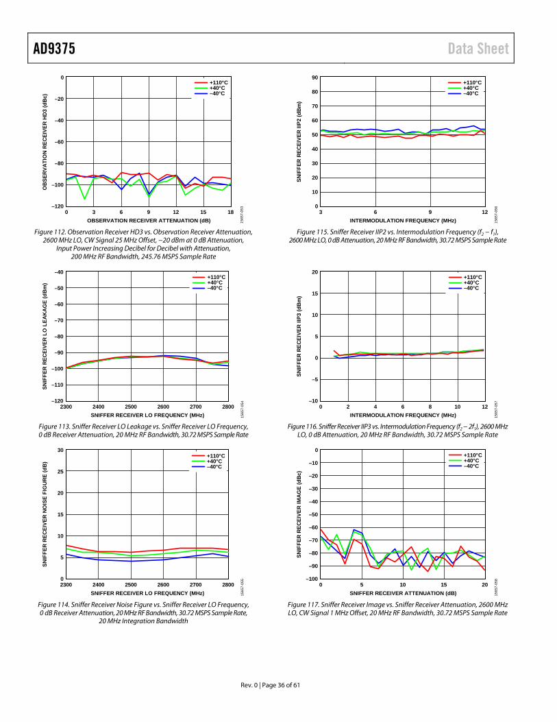
AD9375 Data Sheet
Rev. 0 | Page 36 of 61
0
–120
–100
–80
–60
–40
–20
OBS
ERVA
TIO
N RE
CEIV
ER H
D3 (d
Bc)
0 6 12 183 9 15OBSERVATION RECEIVER ATTENUATION (dB)
+110°C+40°C–40°C
1565
7-05
3
Figure 112. Observation Receiver HD3 vs. Observation Receiver Attenuation,
2600 MHz LO, CW Signal 25 MHz Offset, −20 dBm at 0 dB Attenuation, Input Power Increasing Decibel for Decibel with Attenuation,
200 MHz RF Bandwidth, 245.76 MSPS Sample Rate
–40
–120
–110
–100
–90
–80
–60
–70
–50
SNIF
FER
REC
EIVE
R L
O L
EAK
AG
E (d
Bm
)
2300 2500 2700 28002400 2600SNIFFER RECEIVER LO FREQUENCY (MHz)
+110°C+40°C–40°C
1565
7-05
4
Figure 113. Sniffer Receiver LO Leakage vs. Sniffer Receiver LO Frequency, 0 dB Receiver Attenuation, 20 MHz RF Bandwidth, 30.72 MSPS Sample Rate
30
0
5
10
20
15
25
SNIF
FER
REC
EIVE
R N
OIS
E FI
GU
RE
(dB
)
2300 2500 2700 28002400 2600SNIFFER RECEIVER LO FREQUENCY (MHz)
+110°C+40°C–40°C
1565
7-05
5
Figure 114. Sniffer Receiver Noise Figure vs. Sniffer Receiver LO Frequency, 0 dB Receiver Attenuation, 20 MHz RF Bandwidth, 30.72 MSPS Sample Rate,
20 MHz Integration Bandwidth
90
0
10
20
60
40
80
50
30
70
SNIF
FER
RECE
IVER
IIP2
(dBm
)
3 9 126INTERMODULATION FREQUENCY (MHz)
+110°C+40°C–40°C
1565
7-05
6
Figure 115. Sniffer Receiver IIP2 vs. Intermodulation Frequency (f2 − f1),
2600 MHz LO, 0 dB Attenuation, 20 MHz RF Bandwidth, 30.72 MSPS Sample Rate
20
–10
5
–5
15
0
10
SNIF
FER
RECE
IVER
IIP3
(dBm
)
0 8 124 6 102INTERMODULATION FREQUENCY (MHz)
+110°C+40°C–40°C
1565
7-05
7
Figure 116. Sniffer Receiver IIP3 vs. Intermodulation Frequency (f2 − 2f1), 2600 MHz
LO, 0 dB Attenuation, 20 MHz RF Bandwidth, 30.72 MSPS Sample Rate
0
–100
–90
–70
–40
–80
–50
–20
–60
–30
–10
SNIF
FER
RECE
IVER
IMAG
E (d
Bc)
0 2010 155SNIFFER RECEIVER ATTENUATION (dB)
+110°C+40°C–40°C
1565
7-05
8
Figure 117. Sniffer Receiver Image vs. Sniffer Receiver Attenuation, 2600 MHz LO, CW Signal 1 MHz Offset, 20 MHz RF Bandwidth, 30.72 MSPS Sample Rate
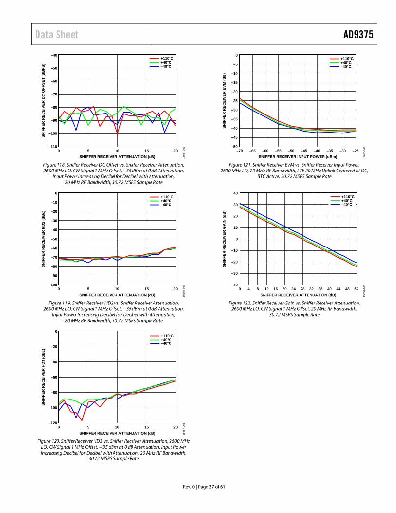
Data Sheet AD9375
Rev. 0 | Page 37 of 61
–40
–110
–100
–80
–90
–70
–50
–60
SNIF
FER
RECE
IVER
DC
OFF
SET
(dBF
S)
0 20155 10SNIFFER RECEIVER ATTENUATION (dB)
+110°C+40°C–40°C
1565
7-05
9
Figure 118. Sniffer Receiver DC Offset vs. Sniffer Receiver Attenuation, 2600 MHz LO, CW Signal 1 MHz Offset, −35 dBm at 0 dB Attenuation,
Input Power Increasing Decibel for Decibel with Attenuation, 20 MHz RF Bandwidth, 30.72 MSPS Sample Rate
0
–100
–90
–70
–80
–60
–20
–40
–50
–10
–30
SNIF
FER
RECE
IVER
HD2
(dBc
)
0 20155 10SNIFFER RECEIVER ATTENUATION (dB)
+110°C+40°C–40°C
1565
7-06
0
Figure 119. Sniffer Receiver HD2 vs. Sniffer Receiver Attenuation,
2600 MHz LO, CW Signal 1 MHz Offset, −35 dBm at 0 dB Attenuation, Input Power Increasing Decibel for Decibel with Attenuation,
20 MHz RF Bandwidth, 30.72 MSPS Sample Rate
0
–120
–100
–40
–80
–20
–60
SNIF
FER
RECE
IVER
HD3
(dBc
)
0 2010 155SNIFFER RECEIVER ATTENUATION (dB)
+110°C+40°C–40°C
1565
7-06
1
Figure 120. Sniffer Receiver HD3 vs. Sniffer Receiver Attenuation, 2600 MHz
LO, CW Signal 1 MHz Offset, −35 dBm at 0 dB Attenuation, Input Power Increasing Decibel for Decibel with Attenuation, 20 MHz RF Bandwidth,
30.72 MSPS Sample Rate
0
–50
–45
–40
–15
–35
–5
–25
–20
–10
–30
SNIF
FER
REC
EIVE
R E
VM (d
B)
–70 –25–40–55 –45 –30–60 –50 –35–65SNIFFER RECEIVER INPUT POWER (dBm)
+110°C+40°C–40°C
1565
7-06
2
Figure 121. Sniffer Receiver EVM vs. Sniffer Receiver Input Power,
2600 MHz LO, 20 MHz RF Bandwidth, LTE 20 MHz Uplink Centered at DC, BTC Active, 30.72 MSPS Sample Rate
40
–40
–30
0
–10
20
–20
10
30
SNIF
FER
RECE
IVER
GAI
N (d
B)
0 5236 4820 32 4412 28 404 24168SNIFFER RECEIVER ATTENUATION (dB)
+110°C+40°C–40°C
1565
7-06
3
Figure 122. Sniffer Receiver Gain vs. Sniffer Receiver Attenuation,
2600 MHz LO, CW Signal 1 MHz Offset, 20 MHz RF Bandwidth, 30.72 MSPS Sample Rate
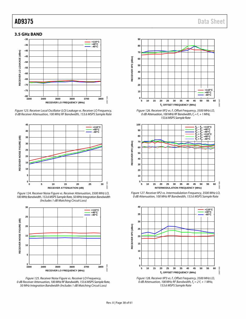
AD9375 Data Sheet
Rev. 0 | Page 38 of 61
3.5 GHz BAND
REC
EIVE
R L
O L
EAK
AG
E (d
Bm
)
RECEIVER LO FREQUENCY (MHz)
–80
–75
–70
–65
–60
–55
–50
–45
–40
–35
–30
3300 3400 3500 3600 3700 3800
+110°C+40°C–40°C
1565
7-06
4
Figure 123. Receiver Local Oscillator (LO) Leakage vs. Receiver LO Frequency, 0 dB Receiver Attenuation, 100 MHz RF Bandwidth, 153.6 MSPS Sample Rate
RECE
IVER
NO
ISE
FIG
URE
(dB)
RECEIVER ATTENUATION (dB)
0
5
10
15
20
25
30
35
40
45
0 5 10 15 20 25 30
+110°C+40°C–40°C
1565
7-06
5
Figure 124. Receiver Noise Figure vs. Receiver Attenuation, 3500 MHz LO,
100 MHz Bandwidth, 153.6 MSPS Sample Rate, 50 MHz Integration Bandwidth (Includes 1 dB Matching Circuit Loss)
REC
EIVE
R N
OIS
E FI
GU
RE
(dB
)
RECEIVER LO FREQUENCY (MHz)
0
5
10
15
20
25
30
3300 3400 3500 3600 3700 3800
+110°C+40°C–40°C
1565
7-06
6
Figure 125. Receiver Noise Figure vs. Receiver LO Frequency, 0 dB Receiver Attenuation, 100 MHz RF Bandwidth, 153.6 MSPS Sample Rate,
50 MHz Integration Bandwidth (Includes 1 dB Matching Circuit Loss)
REC
EIVE
R II
P2 (d
Bm
)
f1 OFFSET FREQUENCY (MHz)
0
10
20
30
40
50
60
70
80
90
5 10 15 20 25 30 35 40 45 50 55 60
+110°C+40°C–40°C
1565
7-06
7
Figure 126. Receiver IIP2 vs. f1 Offset Frequency, 3500 MHz LO,
0 dB Attenuation, 100 MHz RF Bandwidth, f2 = f1 + 1 MHz, 153.6 MSPS Sample Rate
RECE
IVER
IIP2
(dBm
)
INTERMODULATION FREQUENCY (MHz)
0
10
20
30
40
50
60
70
80
90
100
5 10 15 20 25 30 35 40 45 50 55 60
f2 – f1, +110°Cf2 – f1, +40°Cf2 – f1, –40°Cf2 + f1, +110°Cf2 + f1, +40°Cf2 + f1, –40°C
1565
7-06
8
Figure 127. Receiver IIP2 vs. Intermodulation Frequency, 3500 MHz LO,
0 dB Attenuation, 100 MHz RF Bandwidth, 153.6 MSPS Sample Rate
REC
EIVE
R II
P3 (d
Bm
)
f1 OFFSET FREQUENCY (MHz)5 10 15 20 25 30 35 40 45 50 55 60
0
5
10
15
20
25
30
35
40+110°C+40°C–40°C
1565
7-06
9
Figure 128. Receiver IIP3 vs. f1 Offset Frequency, 3500 MHz LO,
0 dB Attenuation, 100 MHz RF Bandwidth, f2 = 2 f1 + 1 MHz, 153.6 MSPS Sample Rate
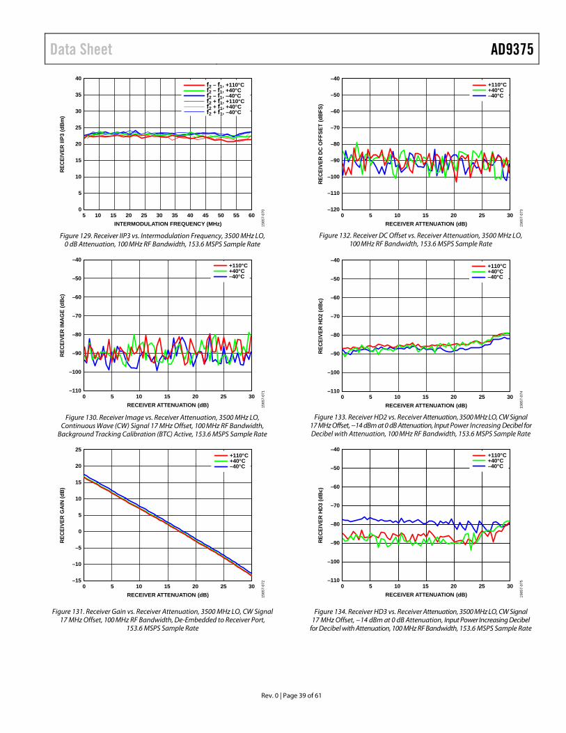
Data Sheet AD9375
Rev. 0 | Page 39 of 61
RECE
IVER
IIP3
(dBm
)
INTERMODULATION FREQUENCY (MHz)5 10 15 20 25 30 35 40 45 50 55 60
0
5
10
15
20
25
30
35
40f2 – f1, +110°Cf2 – f1, +40°Cf2 – f1, –40°Cf2 + f1, +110°Cf2 + f1, +40°Cf2 + f1, –40°C
1565
7-07
0
Figure 129. Receiver IIP3 vs. Intermodulation Frequency, 3500 MHz LO,
0 dB Attenuation, 100 MHz RF Bandwidth, 153.6 MSPS Sample Rate
RECE
IVER
IMAG
E (d
Bc)
RECEIVER ATTENUATION (dB)0 5 10 15 20 25 30
–110
–100
–90
–80
–70
–60
–50
–40+110°C+40°C–40°C
1565
7-07
1
Figure 130. Receiver Image vs. Receiver Attenuation, 3500 MHz LO,
Continuous Wave (CW) Signal 17 MHz Offset, 100 MHz RF Bandwidth, Background Tracking Calibration (BTC) Active, 153.6 MSPS Sample Rate
RECE
IVER
GAI
N (d
B)
RECEIVER ATTENUATION (dB)0 5 10 15 20 25 30
–15
–10
–5
0
5
10
15
20
25+110°C+40°C–40°C
1565
7-07
2
Figure 131. Receiver Gain vs. Receiver Attenuation, 3500 MHz LO, CW Signal 17 MHz Offset, 100 MHz RF Bandwidth, De-Embedded to Receiver Port,
153.6 MSPS Sample Rate
RECE
IVER
DC
OFF
SET
(dBF
S)
RECEIVER ATTENUATION (dB)0 5 10 15 20 25 30
–120
–110
–100
–90
–80
–70
–60
–50
–40+110°C+40°C–40°C
1565
7-07
3
Figure 132. Receiver DC Offset vs. Receiver Attenuation, 3500 MHz LO,
100 MHz RF Bandwidth, 153.6 MSPS Sample Rate
RECE
IVER
HD2
(dBc
)
RECEIVER ATTENUATION (dB)0 5 10 15 20 25 30
–110
–100
–90
–80
–70
–60
–50
–40+110°C+40°C–40°C
1565
7-07
4
Figure 133. Receiver HD2 vs. Receiver Attenuation, 3500 MHz LO, CW Signal
17 MHz Offset, −14 dBm at 0 dB Attenuation, Input Power Increasing Decibel for Decibel with Attenuation, 100 MHz RF Bandwidth, 153.6 MSPS Sample Rate
RECE
IVER
HD3
(dBc
)
RECEIVER ATTENUATION (dB)0 5 10 15 20 25 30
–110
–100
–90
–80
–70
–60
–50
–40+110°C+40°C–40°C
1565
7-07
5
Figure 134. Receiver HD3 vs. Receiver Attenuation, 3500 MHz LO, CW Signal 17 MHz Offset, −14 dBm at 0 dB Attenuation, Input Power Increasing Decibel
for Decibel with Attenuation, 100 MHz RF Bandwidth, 153.6 MSPS Sample Rate
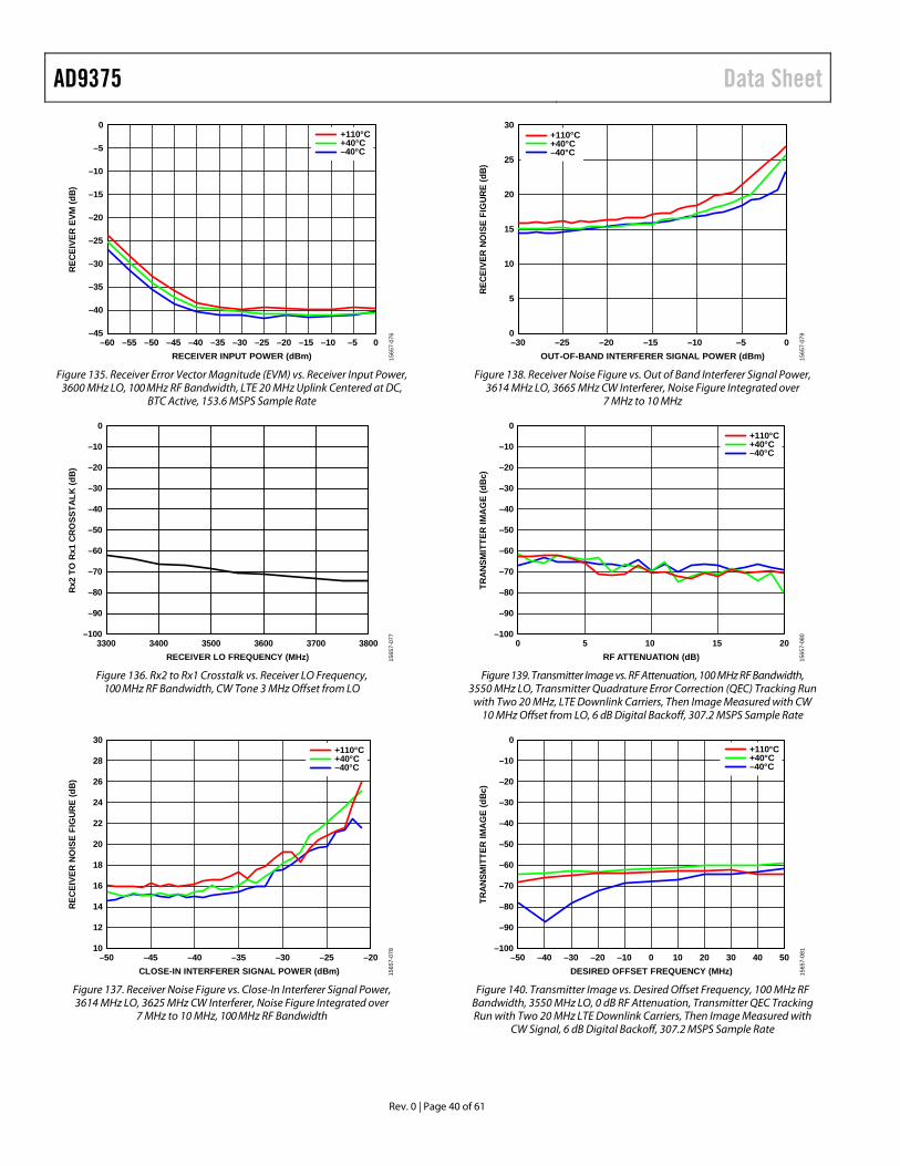
AD9375 Data Sheet
Rev. 0 | Page 40 of 61
RECE
IVER
EVM
(dB)
RECEIVER INPUT POWER (dBm)
–45
–40
–35
–30
–25
–20
–15
–10
–5
0
–60 –55 –50 –45 –40 –35 –30 –25 –20 –15 –10 –5 0
+110°C+40°C–40°C
1565
7-07
6
Figure 135. Receiver Error Vector Magnitude (EVM) vs. Receiver Input Power,
3600 MHz LO, 100 MHz RF Bandwidth, LTE 20 MHz Uplink Centered at DC, BTC Active, 153.6 MSPS Sample Rate
Rx2
TO
Rx1
CR
OSS
TALK
(dB
)
RECEIVER LO FREQUENCY (MHz)
–100
–90
–80
–70
–60
–50
–40
–30
–20
–10
0
3300 3400 3500 3600 3700 3800
1565
7-07
7
Figure 136. Rx2 to Rx1 Crosstalk vs. Receiver LO Frequency,
100 MHz RF Bandwidth, CW Tone 3 MHz Offset from LO
REC
EIVE
R N
OIS
E FI
GU
RE
(dB
)
CLOSE-IN INTERFERER SIGNAL POWER (dBm)
10
12
14
16
18
20
22
24
26
28
30
–50 –45 –40 –35 –30 –25 –20
+110°C+40°C–40°C
1565
7-07
8
Figure 137. Receiver Noise Figure vs. Close-In Interferer Signal Power, 3614 MHz LO, 3625 MHz CW Interferer, Noise Figure Integrated over
7 MHz to 10 MHz, 100 MHz RF Bandwidth
RECE
IVER
NO
ISE
FIG
URE
(dB)
OUT-OF-BAND INTERFERER SIGNAL POWER (dBm)
0
5
10
15
20
25
30
–30 –25 –20 –15 –10 –5 0
+110°C+40°C–40°C
1565
7-07
9
Figure 138. Receiver Noise Figure vs. Out of Band Interferer Signal Power,
3614 MHz LO, 3665 MHz CW Interferer, Noise Figure Integrated over 7 MHz to 10 MHz
TRAN
SMIT
TER
IMAG
E (d
Bc)
RF ATTENUATION (dB)
–100
–90
–80
–70
–60
–50
–40
–30
–20
–10
0
0 5 10 15 20
+110°C+40°C–40°C
1565
7-08
0
Figure 139. Transmitter Image vs. RF Attenuation, 100 MHz RF Bandwidth,
3550 MHz LO, Transmitter Quadrature Error Correction (QEC) Tracking Run with Two 20 MHz, LTE Downlink Carriers, Then Image Measured with CW
10 MHz Offset from LO, 6 dB Digital Backoff, 307.2 MSPS Sample Rate
TRAN
SMIT
TER
IMAG
E (d
Bc)
DESIRED OFFSET FREQUENCY (MHz)
–100
–90
–80
–70
–60
–50
–40
–30
–20
–10
0
–50 –40 –30 –20 –10 0 10 20 30 40 50
+110°C+40°C–40°C
1565
7-08
1
Figure 140. Transmitter Image vs. Desired Offset Frequency, 100 MHz RF
Bandwidth, 3550 MHz LO, 0 dB RF Attenuation, Transmitter QEC Tracking Run with Two 20 MHz LTE Downlink Carriers, Then Image Measured with
CW Signal, 6 dB Digital Backoff, 307.2 MSPS Sample Rate
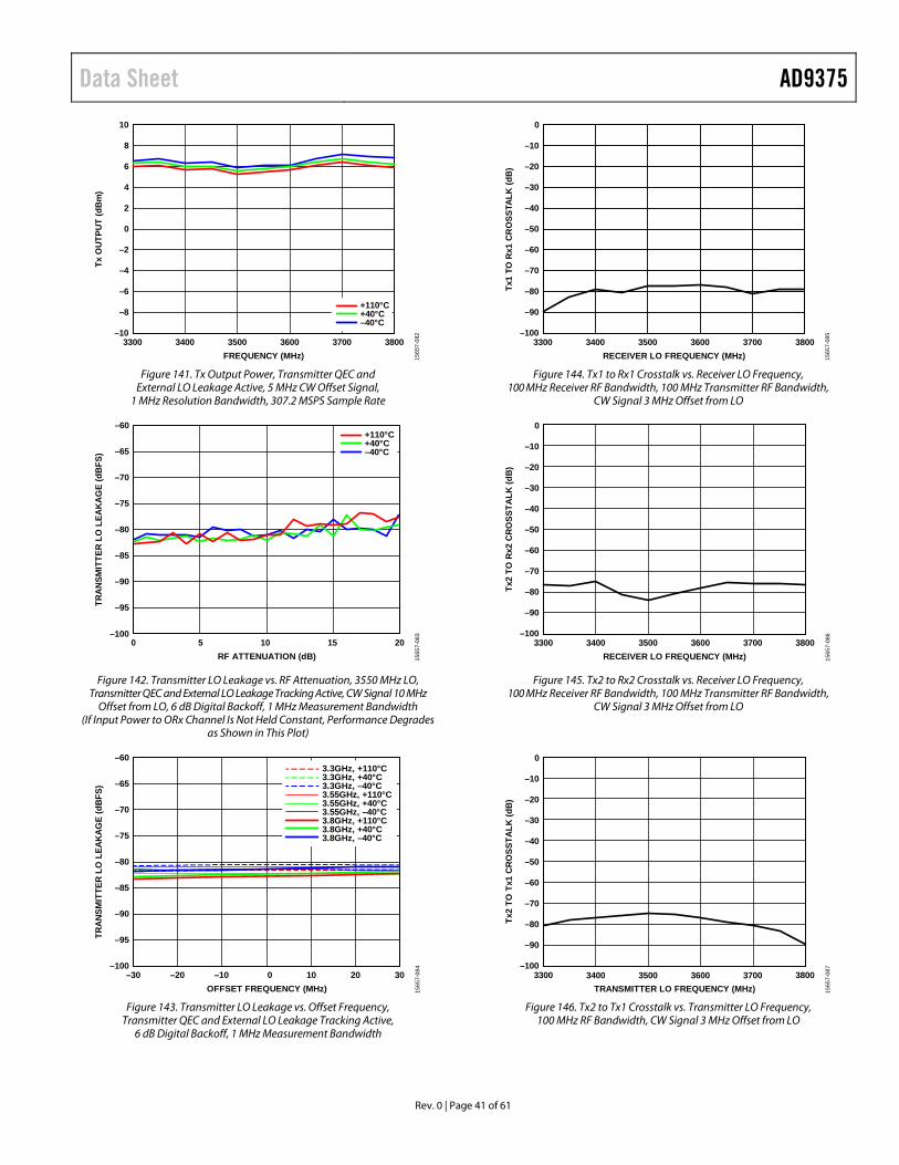
Data Sheet AD9375
Rev. 0 | Page 41 of 61
Tx O
UTP
UT
(dB
m)
FREQUENCY (MHz)
–10
–8
–6
–4
–2
0
2
4
6
8
10
3300 3400 3500 3600 3700 3800
+110°C+40°C–40°C
1565
7-08
2
Figure 141. Tx Output Power, Transmitter QEC and
External LO Leakage Active, 5 MHz CW Offset Signal, 1 MHz Resolution Bandwidth, 307.2 MSPS Sample Rate
0 5 10 15 20
TRAN
SMIT
TER
LO L
EAKA
GE
(dBF
S)
RF ATTENUATION (dB)
–95
–90
–85
–80
–75
–70
–65
–60
–100
+110°C+40°C–40°C
1565
7-08
3
Figure 142. Transmitter LO Leakage vs. RF Attenuation, 3550 MHz LO, Transmitter QEC and External LO Leakage Tracking Active, CW Signal 10 MHz
Offset from LO, 6 dB Digital Backoff, 1 MHz Measurement Bandwidth (If Input Power to ORx Channel Is Not Held Constant, Performance Degrades
as Shown in This Plot)
TRAN
SMIT
TER
LO L
EAKA
GE
(dBF
S)
OFFSET FREQUENCY (MHz)
3.3GHz, +110°C3.3GHz, +40°C3.3GHz, –40°C3.55GHz, +110°C3.55GHz, +40°C3.55GHz, –40°C3.8GHz, +110°C3.8GHz, +40°C3.8GHz, –40°C
–100
–95
–90
–85
–80
–75
–70
–65
–60
–30 –20 –10 0 10 20 30
1565
7-08
4
Figure 143. Transmitter LO Leakage vs. Offset Frequency,
Transmitter QEC and External LO Leakage Tracking Active, 6 dB Digital Backoff, 1 MHz Measurement Bandwidth
Tx1
TOR
x1C
RO
SSTA
LK(d
B)
RECEIVER LO FREQUENCY (MHz)
–100
–90
–80
–70
–60
–50
–40
–30
–20
–10
0
3300 3400 3500 3600 3700 3800
1565
7-08
5
Figure 144. Tx1 to Rx1 Crosstalk vs. Receiver LO Frequency,
100 MHz Receiver RF Bandwidth, 100 MHz Transmitter RF Bandwidth, CW Signal 3 MHz Offset from LO
0
–1003300 3400 3500 3600 3700 3800
Tx2
TO R
x2 C
RO
SSTA
LK (d
B)
RECEIVER LO FREQUENCY (MHz)
–90
–80
–70
–60
–50
–40
–30
–20
–10
1565
7-08
6
Figure 145. Tx2 to Rx2 Crosstalk vs. Receiver LO Frequency, 100 MHz Receiver RF Bandwidth, 100 MHz Transmitter RF Bandwidth,
CW Signal 3 MHz Offset from LO
0
–1003300 3800
Tx2
TO T
x1 C
RO
SSTA
LK (d
B)
TRANSMITTER LO FREQUENCY (MHz)3400 3500 3600 3700
–90
–80
–70
–60
–50
–40
–30
–20
–10
1565
7-08
7
Figure 146. Tx2 to Tx1 Crosstalk vs. Transmitter LO Frequency,
100 MHz RF Bandwidth, CW Signal 3 MHz Offset from LO
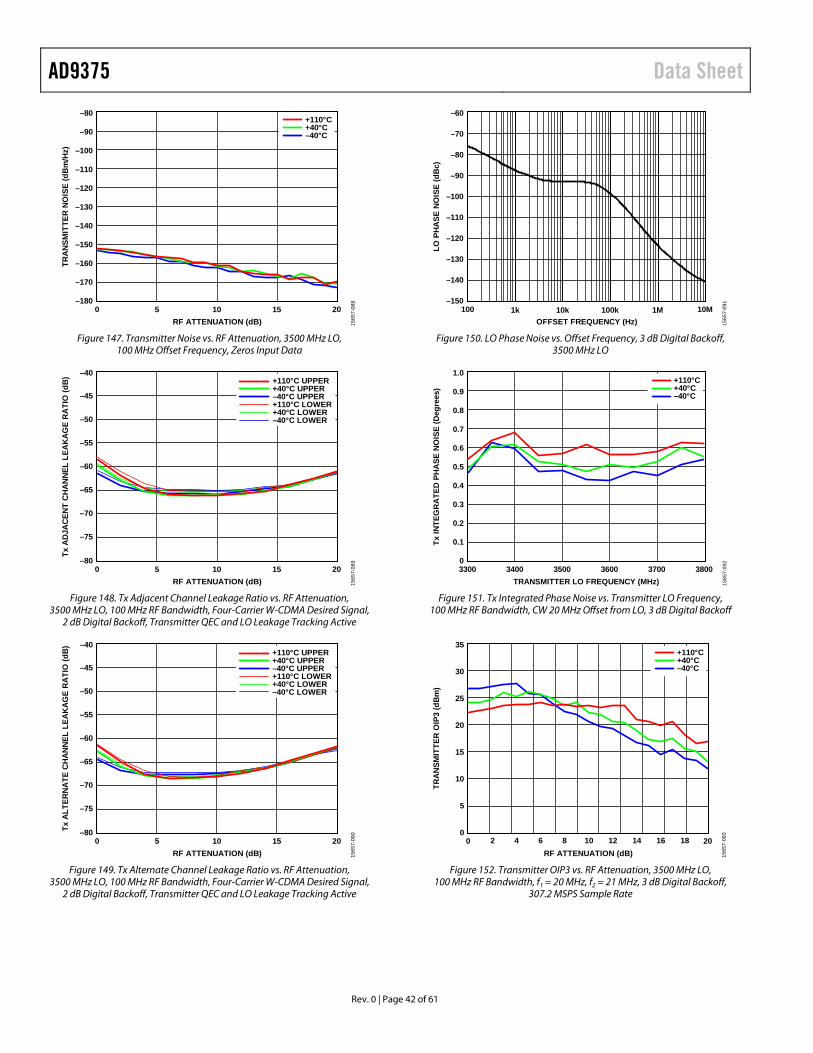
AD9375 Data Sheet
Rev. 0 | Page 42 of 61
–80
–180
TRAN
SMIT
TER
NOIS
E (d
Bm/H
z)
–170
–160
–150
–140
–130
–120
–110
–100
–90
0 205 10 15RF ATTENUATION (dB)
+110°C+40°C–40°C
1565
7-08
8
Figure 147. Transmitter Noise vs. RF Attenuation, 3500 MHz LO,
100 MHz Offset Frequency, Zeros Input Data
0 205 10 15
–40
–80
Tx A
DJAC
ENT
CHAN
NEL
LEAK
AGE
RATI
O (d
B)
RF ATTENUATION (dB)
–75
–70
–65
–60
–55
–50
–45
+110°C UPPER+40°C UPPER–40°C UPPER+110°C LOWER+40°C LOWER–40°C LOWER
1565
7-08
9
Figure 148. Tx Adjacent Channel Leakage Ratio vs. RF Attenuation,
3500 MHz LO, 100 MHz RF Bandwidth, Four-Carrier W-CDMA Desired Signal, 2 dB Digital Backoff, Transmitter QEC and LO Leakage Tracking Active
–40
–800 20
Tx A
LTER
NATE
CHA
NNEL
LEA
KAG
E RA
TIO
(dB)
RF ATTENUATION (dB)
–75
–70
–65
–60
–55
–50
–45
5 10 15
+110°C UPPER+40°C UPPER–40°C UPPER+110°C LOWER+40°C LOWER–40°C LOWER
1565
7-09
0
Figure 149. Tx Alternate Channel Leakage Ratio vs. RF Attenuation,
3500 MHz LO, 100 MHz RF Bandwidth, Four-Carrier W-CDMA Desired Signal, 2 dB Digital Backoff, Transmitter QEC and LO Leakage Tracking Active
–60
–150100 10M
LO P
HA
SE N
OIS
E (d
Bc)
OFFSET FREQUENCY (Hz)
–140
–130
–120
–110
–100
–90
–80
–70
1k 10k 100k 1M
1565
7-09
1
Figure 150. LO Phase Noise vs. Offset Frequency, 3 dB Digital Backoff,
3500 MHz LO
1.0
03300 3800
Tx IN
TEG
RA
TED
PH
ASE
NO
ISE
(Deg
rees
)
TRANSMITTER LO FREQUENCY (MHz)
0.1
0.2
0.3
0.4
0.5
0.6
0.7
0.8
0.9
3400 3500 3600 3700
+110°C+40°C–40°C
1565
7-09
2
Figure 151. Tx Integrated Phase Noise vs. Transmitter LO Frequency,
100 MHz RF Bandwidth, CW 20 MHz Offset from LO, 3 dB Digital Backoff
35
00 20
TRAN
SMIT
TER
OIP
3 (d
Bm)
RF ATTENUATION (dB)
5
10
15
20
25
30
2 4 6 8 10 12 14 16 18
+110°C+40°C–40°C
1565
7-09
3
Figure 152. Transmitter OIP3 vs. RF Attenuation, 3500 MHz LO,
100 MHz RF Bandwidth, f1 = 20 MHz, f2 = 21 MHz, 3 dB Digital Backoff, 307.2 MSPS Sample Rate
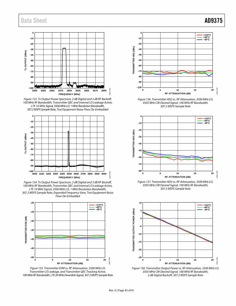
Data Sheet AD9375
Rev. 0 | Page 43 of 61
3400 3600FREQUENCY (MHz)
0
–100
Tx O
UTP
UT
(dB
m)
–90
–80
–70
–60
–50
–40
–30
–20
–10
3425 3450 3475 3500 3525 3550 3575
1565
7-09
4
Figure 153. Tx Output Power Spectrum, 2 dB Digital and 3 dB RF Backoff,
100 MHz RF Bandwidth, Transmitter QEC and Internal LO Leakage Active, LTE 10 MHz Signal, 3500 MHz LO, 1 MHz Resolution Bandwidth,
307.2 MSPS Sample Rate, Test Equipment Noise Floor De-Embedded
0
–1003000 4000
Tx O
UTP
UT
(dB
m)
FREQUENCY (MHz)
–90
–80
–70
–60
–50
–40
–30
–20
–10
3100 3200 3300 3400 3500 3600 3700 3800 3900
1565
7-09
5
Figure 154. Tx Output Power Spectrum, 2 dB Digital and 3 dB RF Backoff,
100 MHz RF Bandwidth, Transmitter QEC and Internal LO Leakage Active, LTE 10 MHz Signal, 3500 MHz LO, 1 MHz Resolution Bandwidth,
307.2 MSPS Sample Rate, Expanded Frequency View, Test Equipment Noise Floor De-Embedded
–20
–500 20
TRAN
SMIT
TER
EVM
(dB)
RF ATTENUATION (dB)
–45
–40
–35
–30
–25
5 10 15
+110°C+40°C–40°C
1565
7-09
6
Figure 155. Transmitter EVM vs. RF Attenuation, 3500 MHz LO, Transmitter LO Leakage, and Transmitter QEC Tracking Active,
100 MHz RF Bandwidth, LTE 20 MHz Downlink Signal, 307.2 MSPS Sample Rate
0
–1000 20
TRAN
SMIT
TER
HD2
(dBc
)
RF ATTENUATION (dB)
–90
–80
–70
–60
–50
–40
–30
–20
–10
5 10 15
+110°C+40°C–40°C
1565
7-09
7
Figure 156. Transmitter HD2 vs. RF Attenuation, 3500 MHz LO, 3505 MHz CW Desired Signal, 100 MHz RF Bandwidth,
307.2 MSPS Sample Rate
0
–800 20
TRAN
SMIT
TER
HD3
(dBc
)
RF ATTENUATION (dB)
–70
–60
–50
–40
–30
–20
–10
5 10 15
+110°C+40°C–40°C
1565
7-09
8
Figure 157. Transmitter HD3 vs. RF Attenuation, 3500 MHz LO,
3505 MHz CW Desired Signal, 100 MHz RF Bandwidth, 307.2 MSPS Sample Rate
10
–250 20
TRAN
SMIT
TER
OUT
PUT
POW
ER (d
Bm)
RF ATTENUATION (dB)
–20
–15
–10
–5
0
5
5 10 15
+110°C+40°C–40°C
1565
7-09
9
Figure 158. Transmitter Output Power vs. RF Attenuation, 3500 MHz LO,
3505 MHz CW Desired Signal, 100 MHz RF Bandwidth, 2 dB Digital Backoff, 307.2 MSPS Sample Rate
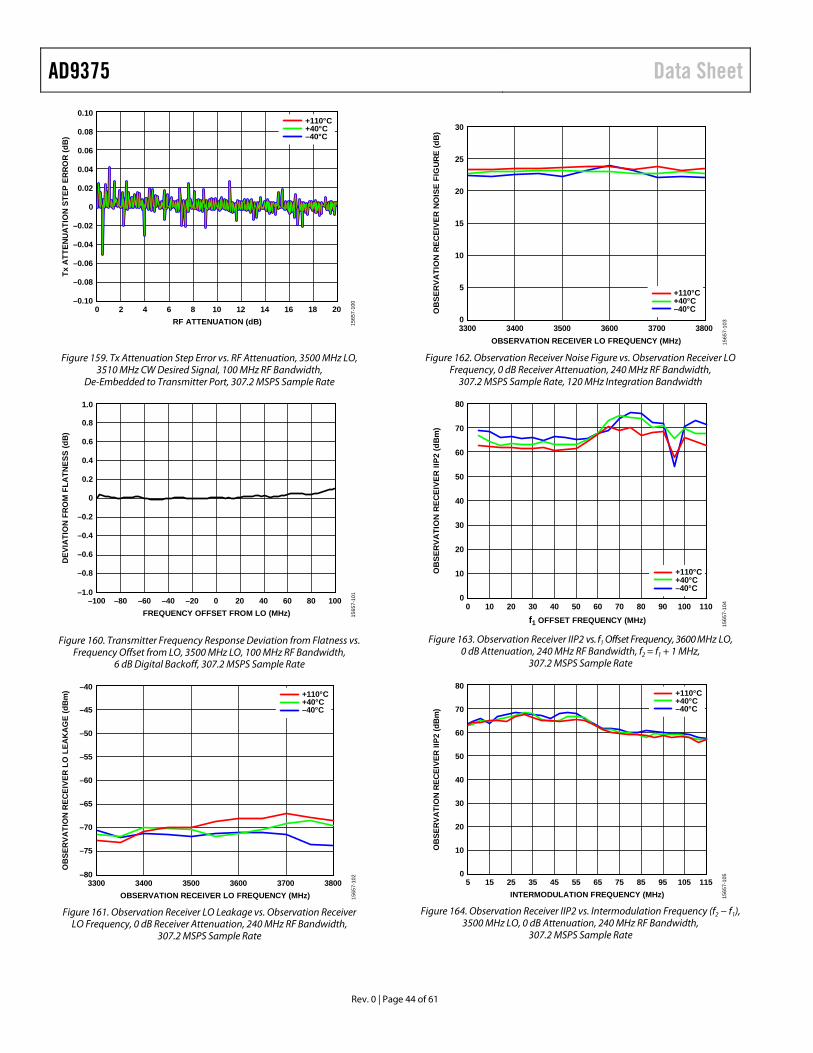
AD9375 Data Sheet
Rev. 0 | Page 44 of 61
0.10
–0.100 20
Tx A
TTEN
UATI
ON
STEP
ERR
OR
(dB)
RF ATTENUATION (dB)
–0.08
–0.06
–0.04
–0.02
0
0.02
0.04
0.06
0.08
2 4 6 8 10 12 14 16 18
+110°C+40°C–40°C
1565
7-10
0
Figure 159. Tx Attenuation Step Error vs. RF Attenuation, 3500 MHz LO, 3510 MHz CW Desired Signal, 100 MHz RF Bandwidth,
De-Embedded to Transmitter Port, 307.2 MSPS Sample Rate
1.0
–1.0–100 100
DEV
IATI
ON
FR
OM
FLA
TNES
S (d
B)
FREQUENCY OFFSET FROM LO (MHz)
–0.8
–0.6
–0.4
–0.2
0
0.2
0.4
0.6
0.8
–80 –60 –40 –20 0 20 40 60 80
1565
7-10
1
Figure 160. Transmitter Frequency Response Deviation from Flatness vs. Frequency Offset from LO, 3500 MHz LO, 100 MHz RF Bandwidth,
6 dB Digital Backoff, 307.2 MSPS Sample Rate
–40
–803300 3800
OB
SER
VATI
ON
REC
EIVE
R L
O L
EAK
AG
E (d
Bm
)
OBSERVATION RECEIVER LO FREQUENCY (MHz)
–75
–70
–65
–60
–55
–50
–45
3400 3500 3600 3700
+110°C+40°C–40°C
1565
7-10
2
Figure 161. Observation Receiver LO Leakage vs. Observation Receiver
LO Frequency, 0 dB Receiver Attenuation, 240 MHz RF Bandwidth, 307.2 MSPS Sample Rate
30
03300 3800
OB
SER
VATI
ON
REC
EIVE
R N
OIS
E FI
GU
RE
(dB
)
OBSERVATION RECEIVER LO FREQUENCY (MHz)
5
10
15
20
25
3400 3500 3600 3700
+110°C+40°C–40°C
1565
7-10
3
Figure 162. Observation Receiver Noise Figure vs. Observation Receiver LO
Frequency, 0 dB Receiver Attenuation, 240 MHz RF Bandwidth, 307.2 MSPS Sample Rate, 120 MHz Integration Bandwidth
80
00 110
OB
SER
VATI
ON
REC
EIVE
R II
P2 (d
Bm
)
f1 OFFSET FREQUENCY (MHz)
10
20
30
40
50
60
70
10 20 30 40 50 60 70 80 90 100
+110°C+40°C–40°C
1565
7-10
4
Figure 163. Observation Receiver IIP2 vs. f1 Offset Frequency, 3600 MHz LO,
0 dB Attenuation, 240 MHz RF Bandwidth, f2 = f1 + 1 MHz, 307.2 MSPS Sample Rate
80
05 115
OB
SER
VATI
ON
REC
EIVE
R II
P2 (d
Bm
)
INTERMODULATION FREQUENCY (MHz)15 25 35 45 55 65 75 85 95 105
10
20
30
40
50
60
70
+110°C+40°C–40°C
1565
7-10
5
Figure 164. Observation Receiver IIP2 vs. Intermodulation Frequency (f2 − f1),
3500 MHz LO, 0 dB Attenuation, 240 MHz RF Bandwidth, 307.2 MSPS Sample Rate
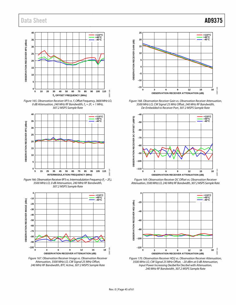
Data Sheet AD9375
Rev. 0 | Page 45 of 61
40
00 110
OB
SER
VATI
ON
REC
EIVE
R II
P3 (d
Bm
)
f1 OFFSET FREQUENCY (MHz)
5
10
15
20
25
30
35
10 20 30 40 50 60 70 80 90 100
+110°C+40°C–40°C
1565
7-10
6
Figure 165. Observation Receiver IIP3 vs. f1 Offset Frequency, 3600 MHz LO,
0 dB Attenuation, 240 MHz RF Bandwidth, f2 = 2f1 + 1 MHz, 307.2 MSPS Sample Rate
40
05 115
OB
SER
VATI
ON
REC
EIVE
R II
P3 (d
Bm
)
INTERMODULATION FREQUENCY (MHz)
5
10
15
20
25
30
35
15 25 35 45 55 65 75 85 95 105
+110°C+40°C–40°C
1565
7-10
7
Figure 166. Observation Receiver IIP3 vs. Intermodulation Frequency (f2 − 2f1),
3500 MHz LO, 0 dB Attenuation, 240 MHz RF Bandwidth, 307.2 MSPS Sample Rate
0
–1000 18
OBS
ERVA
TIO
N RE
CEIV
ER IM
AGE
(dBc
)
OBSERVATION RECEIVER ATTENUATION (dB)
–90
–80
–70
–60
–50
–40
–30
–20
–10
3 6 9 12 15
+110°C+40°C–40°C
1565
7-10
8
Figure 167. Observation Receiver Image vs. Observation Receiver
Attenuation, 3500 MHz LO, CW Signal 25 MHz Offset, 240 MHz RF Bandwidth, BTC Active, 307.2 MSPS Sample Rate
25
–150 18
OBS
ERVA
TIO
N RE
CEIV
ER G
AIN
(dB)
OBSERVATION RECEIVER ATTENUATION (dB)
–10
–5
0
5
10
15
20
3 6 9 12 15
+110°C+40°C–40°C
1565
7-10
9
Figure 168. Observation Receiver Gain vs. Observation Receiver Attenuation, 3500 MHz LO, CW Signal 25 MHz Offset, 240 MHz RF Bandwidth,
De-Embedded to Receiver Port, 307.2 MSPS Sample Rate
–40
–1100 18
OBS
ERVA
TIO
N RE
CEIV
ER D
C O
FFSE
T (d
BFS)
OBSERVATION RECEIVER ATTENUATION (dB)
–100
–90
–80
–70
–60
–50
3 6 9 12 15
+110°C+40°C–40°C
1565
7-11
0
Figure 169. Observation Receiver DC Offset vs. Observation Receiver
Attenuation, 3500 MHz LO, 240 MHz RF Bandwidth, 307.2 MSPS Sample Rate
0
–1200 18
OBS
ERVA
TIO
N RE
CEIV
ER H
D2 (d
Bc)
OBSERVATION RECEIVER ATTENUATION (dB)
–100
–80
–60
–40
–20
3 6 9 12 15
+110°C+40°C–40°C
1565
7-11
1
Figure 170. Observation Receiver HD2 vs. Observation Receiver Attenuation,
3500 MHz LO, CW Signal 25 MHz Offset, −20 dBm at 0 dB Attenuation, Input Power Increasing Decibel for Decibel with Attenuation,
240 MHz RF Bandwidth, 307.2 MSPS Sample Rate
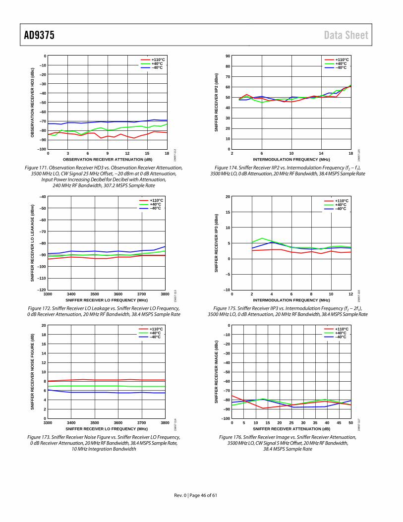
AD9375 Data Sheet
Rev. 0 | Page 46 of 61
0
–1000 18
OBS
ERVA
TIO
N RE
CEIV
ER H
D3 (d
Bc)
OBSERVATION RECEIVER ATTENUATION (dB)
–90
–80
–70
–60
–50
–40
–30
–20
–10
3 6 9 12 15
+110°C+40°C–40°C
1565
7-11
2
Figure 171. Observation Receiver HD3 vs. Observation Receiver Attenuation,
3500 MHz LO, CW Signal 25 MHz Offset, −20 dBm at 0 dB Attenuation, Input Power Increasing Decibel for Decibel with Attenuation,
240 MHz RF Bandwidth, 307.2 MSPS Sample Rate
–40
–120
SNIF
FER
REC
EIVE
R L
O L
EAK
AG
E (d
Bm
)
SNIFFER RECEIVER LO FREQUENCY (MHz)
–110
–100
–90
–80
–70
–60
–50
3300 38003400 3500 3600 3700
+110°C+40°C–40°C
1565
7-11
3
Figure 172. Sniffer Receiver LO Leakage vs. Sniffer Receiver LO Frequency, 0 dB Receiver Attenuation, 20 MHz RF Bandwidth, 38.4 MSPS Sample Rate
20
03300 3800
SNIF
FER
REC
EIVE
R N
OIS
E FI
GU
RE
(dB
)
SNIFFER RECEIVER LO FREQUENCY (MHz)3400 3500 3600 3700
2
4
6
8
10
12
14
16
18+110°C+40°C–40°C
1565
7-11
4
Figure 173. Sniffer Receiver Noise Figure vs. Sniffer Receiver LO Frequency,
0 dB Receiver Attenuation, 20 MHz RF Bandwidth, 38.4 MSPS Sample Rate, 10 MHz Integration Bandwidth
90
02 18
SNIF
FER
RECE
IVER
IIP2
(dBm
)
INTERMODULATION FREQUENCY (MHz)
10
20
30
40
50
60
70
80
6 10 14
+110°C+40°C–40°C
1565
7-11
5
Figure 174. Sniffer Receiver IIP2 vs. Intermodulation Frequency (f2 − f1),
3500 MHz LO, 0 dB Attenuation, 20 MHz RF Bandwidth, 38.4 MSPS Sample Rate
20
–100 12
SNIF
FER
RECE
IVER
IIP3
(dBm
)
INTERMODULATION FREQUENCY (MHz)
–5
0
5
10
15
2 4 6 8 10
+110°C+40°C–40°C
1565
7-11
6
Figure 175. Sniffer Receiver IIP3 vs. Intermodulation Frequency (f2 − 2f1),
3500 MHz LO, 0 dB Attenuation, 20 MHz RF Bandwidth, 38.4 MSPS Sample Rate
0
–1000 50
SNIF
FER
RECE
IVER
IMAG
E (d
Bc)
SNIFFER RECEIVER ATTENUATION (dB)
–90
–80
–70
–60
–50
–40
–30
–20
–10
5 10 15 20 25 30 35 40 45
+110°C+40°C–40°C
1565
7-11
7
Figure 176. Sniffer Receiver Image vs. Sniffer Receiver Attenuation,
3500 MHz LO, CW Signal 5 MHz Offset, 20 MHz RF Bandwidth, 38.4 MSPS Sample Rate
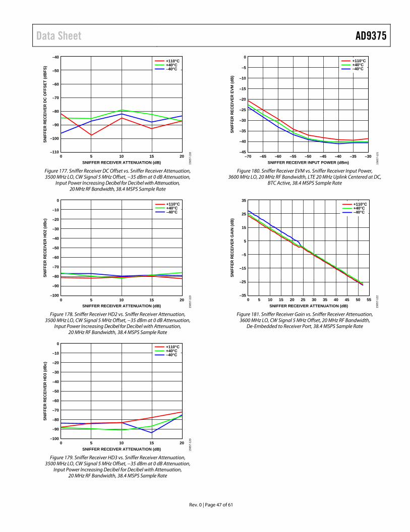
Data Sheet AD9375
Rev. 0 | Page 47 of 61
–40
–1100 20
SNIF
FER
RECE
IVER
DC
OFF
SET
(dBF
S)
SNIFFER RECEIVER ATTENUATION (dB)
–100
–90
–80
–70
–60
–50
5 10 15
+110°C+40°C–40°C
1565
7-11
8
Figure 177. Sniffer Receiver DC Offset vs. Sniffer Receiver Attenuation, 3500 MHz LO, CW Signal 5 MHz Offset, −35 dBm at 0 dB Attenuation,
Input Power Increasing Decibel for Decibel with Attenuation, 20 MHz RF Bandwidth, 38.4 MSPS Sample Rate
0
–1000 20
SNIF
FER
RECE
IVER
HD2
(dBc
)
SNIFFER RECEIVER ATTENUATION (dB)
–90
–80
–70
–60
–50
–40
–30
–20
–10
5 10 15
+110°C+40°C–40°C
1565
7-11
9
Figure 178. Sniffer Receiver HD2 vs. Sniffer Receiver Attenuation,
3500 MHz LO, CW Signal 5 MHz Offset, −35 dBm at 0 dB Attenuation, Input Power Increasing Decibel for Decibel with Attenuation,
20 MHz RF Bandwidth, 38.4 MSPS Sample Rate
0
–100
–90
–80
–70
–60
–50
–40
–30
–20
0 20
SNIF
FER
RECE
IVER
HD3
(dBc
)
SNIFFER RECEIVER ATTENUATION (dB)
–10
5 10 15
+110°C+40°C–40°C
1565
7-12
0
Figure 179. Sniffer Receiver HD3 vs. Sniffer Receiver Attenuation,
3500 MHz LO, CW Signal 5 MHz Offset, −35 dBm at 0 dB Attenuation, Input Power Increasing Decibel for Decibel with Attenuation,
20 MHz RF Bandwidth, 38.4 MSPS Sample Rate
0
–45–70 –30
SNIF
FER
REC
EIVE
R E
VM (d
B)
SNIFFER RECEIVER INPUT POWER (dBm)
–40
–35
–30
–25
–20
–15
–10
–5
–65 –60 –55 –50 –45 –40 –35
+110°C+40°C–40°C
1565
7-12
1
Figure 180. Sniffer Receiver EVM vs. Sniffer Receiver Input Power,
3600 MHz LO, 20 MHz RF Bandwidth, LTE 20 MHz Uplink Centered at DC, BTC Active, 38.4 MSPS Sample Rate
35
–350 55
SNIF
FER
RECE
IVER
GAI
N (d
B)
SNIFFER RECEIVER ATTENUATION (dB)
–25
–15
–5
5
15
25
5 10 15 20 25 30 35 40 45 50
+110°C+40°C–40°C
1565
7-12
2
Figure 181. Sniffer Receiver Gain vs. Sniffer Receiver Attenuation,
3600 MHz LO, CW Signal 5 MHz Offset, 20 MHz RF Bandwidth, De-Embedded to Receiver Port, 38.4 MSPS Sample Rate
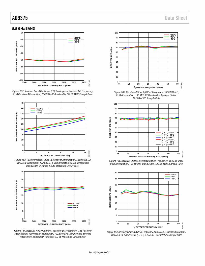
AD9375 Data Sheet
Rev. 0 | Page 48 of 61
5.5 GHz BAND –30
–1005300 5900
REC
EIVE
R L
O L
EAK
AG
E (d
Bm
)
RECEIVER LO FREQUENCY (MHz)
–90
–80
–70
–60
–50
–40
5400 5500 5600 5700 5800
+110°C+40°C–40°C
1565
7-22
3
Figure 182. Receiver Local Oscillator (LO) Leakage vs. Receiver LO Frequency, 0 dB Receiver Attenuation, 100 MHz RF Bandwidth, 122.88 MSPS Sample Rate
45
00 15
RECE
IVER
NO
ISE
FIG
URE
(dB)
RECEIVER ATTENUATION (dB)
5
10
15
20
25
35
30
40
3 6 9 12
+110°C+40°C–40°C
1565
7-22
4
Figure 183. Receiver Noise Figure vs. Receiver Attenuation, 5600 MHz LO,
100 MHz Bandwidth, 122.88 MSPS Sample Rate, 50 MHz Integration Bandwidth (Includes 1.2 dB Matching Circuit Loss)
30
05300 5900
REC
EIVE
R N
OIS
E FI
GU
RE
(dB
)
RECEIVER LO FREQUENCY (MHz)
5
10
15
20
25
5400 5500 5600 5700 5800
+110°C+40°C–40°C
1565
7-22
5
Figure 184. Receiver Noise Figure vs. Receiver LO Frequency, 0 dB Receiver Attenuation, 100 MHz RF Bandwidth, 122.88 MSPS Sample Rate, 50 MHz
Integration Bandwidth (Includes 1.2 dB Matching Circuit Loss)
100
90
80
70
60
50
40
30
20
10
00 60
RE
CE
IVE
R II
P2
(dB
m)
f1 OFFSET FREQUENCY (MHz)20 4010 30 50
+110°C+40°C–40°C
1565
7-18
5
Figure 185. Receiver IIP2 vs. f1 Offset Frequency, 5600 MHz LO,
0 dB Attenuation, 100 MHz RF Bandwidth, f2 = f1 + 1 MHz, 122.88 MSPS Sample Rate
100
015 45
RECE
IVER
IIP2
(dBm
)
INTERMODULATION FREQUENCY (MHz)
10
30
50
70
90
20
40
60
80
20 25 30 35 40
f2 + f1, +110°Cf2 + f1, +40°Cf2 + f1, –40°Cf2 – f1, +110°Cf2 – f1, +40°Cf2 – f1, –40°C
1565
7-22
6
Figure 186. Receiver IIP2 vs. Intermodulation Frequency, 5600 MHz LO, 0 dB Attenuation, 100 MHz RF Bandwidth, 122.88 MSPS Sample Rate
40
35
30
25
20
15
10
5
00 60
REC
EIVE
R II
P3 (d
Bm
)
f1 OFFSET FREQUENCY (MHz)20 4010 30 50
+110°C+40°C–40°C
1565
7-18
7
Figure 187. Receiver IIP3 vs. f1 Offset Frequency, 5600 MHz LO, 0 dB Attenuation,
100 MHz RF Bandwidth, f2 = 2 f1 + 2 MHz, 122.88 MSPS Sample Rate
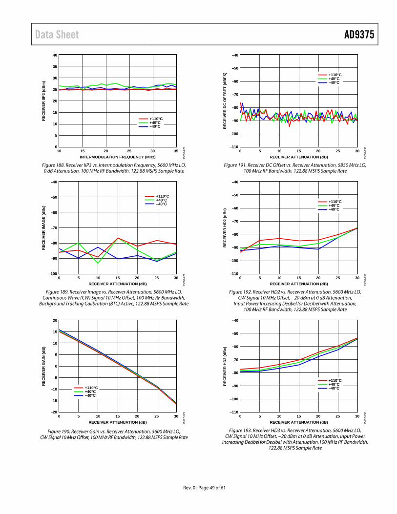
Data Sheet AD9375
Rev. 0 | Page 49 of 61
40
010 15 35
RECE
IVER
IIP3
(dBm
)
INTERMODULATION FREQUENCY (MHz)
10
20
5
15
25
30
35
20 25 30
+110°C+40°C–40°C
1565
7-22
7
Figure 188. Receiver IIP3 vs. Intermodulation Frequency, 5600 MHz LO, 0 dB Attenuation, 100 MHz RF Bandwidth, 122.88 MSPS Sample Rate
–40
–1000 30
RECE
IVER
IMAG
E (d
Bc)
RECEIVER ATTENUATION (dB)
–80
–90
–70
–60
–50
5 15 2510 20
+110°C+40°C–40°C
1565
7-22
8
Figure 189. Receiver Image vs. Receiver Attenuation, 5600 MHz LO,
Continuous Wave (CW) Signal 10 MHz Offset, 100 MHz RF Bandwidth, Background Tracking Calibration (BTC) Active, 122.88 MSPS Sample Rate
20
–200 30
RECE
IVER
GAI
N (d
B)
RECEIVER ATTENUATION (dB)
–10
–15
–5
5
15
0
10
5 15 2510 20
+110°C+40°C–40°C
1565
7-22
9
Figure 190. Receiver Gain vs. Receiver Attenuation, 5600 MHz LO, CW Signal 10 MHz Offset, 100 MHz RF Bandwidth, 122.88 MSPS Sample Rate
–40
–1100 30
RECE
IVER
DC
OFF
SET
(dBF
S)
RECEIVER ATTENUATION (dB)
–90
–100
–80
–60
–70
–50
5 15 2510 20
+110°C+40°C–40°C
1565
7-23
0
Figure 191. Receiver DC Offset vs. Receiver Attenuation, 5850 MHz LO,
100 MHz RF Bandwidth, 122.88 MSPS Sample Rate
–40
–1100 30
RECE
IVER
HD2
(dBc
)
RECEIVER ATTENUATION (dB)
–90
–100
–80
–60
–70
–50
5 15 2510 20
+110°C+40°C–40°C
1565
7-23
1
Figure 192. Receiver HD2 vs. Receiver Attenuation, 5600 MHz LO,
CW Signal 10 MHz Offset, −20 dBm at 0 dB Attenuation, Input Power Increasing Decibel for Decibel with Attenuation,
100 MHz RF Bandwidth, 122.88 MSPS Sample Rate
–40
–1100 30
RECE
IVER
HD3
(dBc
)
RECEIVER ATTENUATION (dB)
–90
–100
–80
–60
–70
–50
5 15 2510 20
+110°C+40°C–40°C
1565
7-23
2
Figure 193. Receiver HD3 vs. Receiver Attenuation, 5600 MHz LO,
CW Signal 10 MHz Offset, −20 dBm at 0 dB Attenuation, Input Power Increasing Decibel for Decibel with Attenuation,100 MHz RF Bandwidth,
122.88 MSPS Sample Rate
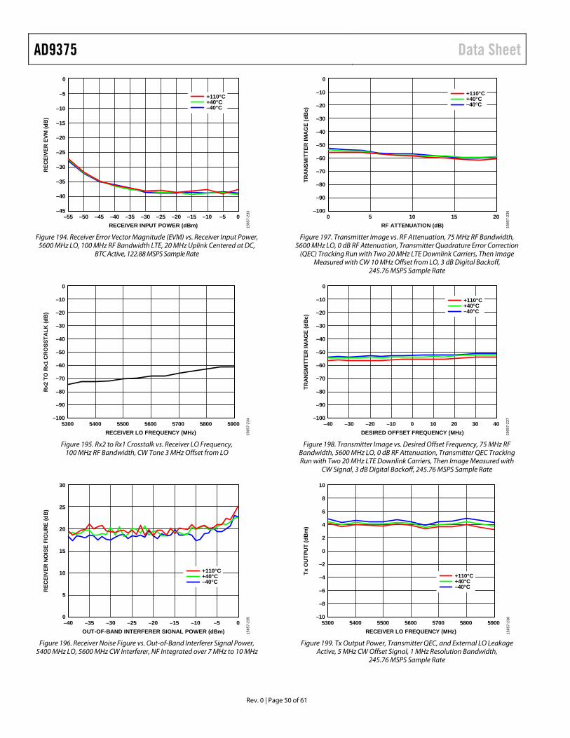
AD9375 Data Sheet
Rev. 0 | Page 50 of 61
0
–45–55 0
RECE
IVER
EVM
(dB)
RECEIVER INPUT POWER (dBm)
–35
–40
–30
–15
–25
–5
–20
–10
–45 –25 –5–35 –15–50 –30 –10–40 –20
+110°C+40°C–40°C
1565
7-23
3
Figure 194. Receiver Error Vector Magnitude (EVM) vs. Receiver Input Power,
5600 MHz LO, 100 MHz RF Bandwidth LTE, 20 MHz Uplink Centered at DC, BTC Active, 122.88 MSPS Sample Rate
0
–1005300 5900
Rx2
TO
Rx1
CR
OSS
TALK
(dB
)
RECEIVER LO FREQUENCY (MHz)
–70
–80
–90
–60
–30
–50
–10
–40
–20
5500 57005400 58005600
1565
7-23
4
Figure 195. Rx2 to Rx1 Crosstalk vs. Receiver LO Frequency,
100 MHz RF Bandwidth, CW Tone 3 MHz Offset from LO
30
0–40 0
RECE
IVER
NO
ISE
FIG
URE
(dB)
OUT-OF-BAND INTERFERER SIGNAL POWER (dBm)
15
5
25
10
20
–25 –5–35 –15–30 –10–20
+110°C+40°C–40°C
1565
7-23
5
Figure 196. Receiver Noise Figure vs. Out-of-Band Interferer Signal Power,
5400 MHz LO, 5600 MHz CW Interferer, NF Integrated over 7 MHz to 10 MHz
0
–1000 20
TRAN
SMIT
TER
IMAG
E (d
Bc)
RF ATTENUATION (dB)
–70
–80
–90
–60
–30
–50
–10
–40
–20
105 15
+110°C+40°C–40°C
1565
7-23
6
Figure 197. Transmitter Image vs. RF Attenuation, 75 MHz RF Bandwidth,
5600 MHz LO, 0 dB RF Attenuation, Transmitter Quadrature Error Correction (QEC) Tracking Run with Two 20 MHz LTE Downlink Carriers, Then Image
Measured with CW 10 MHz Offset from LO, 3 dB Digital Backoff, 245.76 MSPS Sample Rate
0
–100–40 40
TRAN
SMIT
TER
IMAG
E (d
Bc)
DESIRED OFFSET FREQUENCY (MHz)
–70
–80
–90
–60
–30
–50
–10
–40
–20
0–20 20 30–10–30 10
+110°C+40°C–40°C
1565
7-23
7
Figure 198. Transmitter Image vs. Desired Offset Frequency, 75 MHz RF
Bandwidth, 5600 MHz LO, 0 dB RF Attenuation, Transmitter QEC Tracking Run with Two 20 MHz LTE Downlink Carriers, Then Image Measured with
CW Signal, 3 dB Digital Backoff, 245.76 MSPS Sample Rate
10
–105300 5900
Tx O
UTP
UT
(dB
m)
RECEIVER LO FREQUENCY (MHz)
–8
–4
0
4
8
–6
–2
2
6
5400 5500 5600 5700 5800
+110°C+40°C–40°C
1565
7-23
8
Figure 199. Tx Output Power, Transmitter QEC, and External LO Leakage
Active, 5 MHz CW Offset Signal, 1 MHz Resolution Bandwidth, 245.76 MSPS Sample Rate
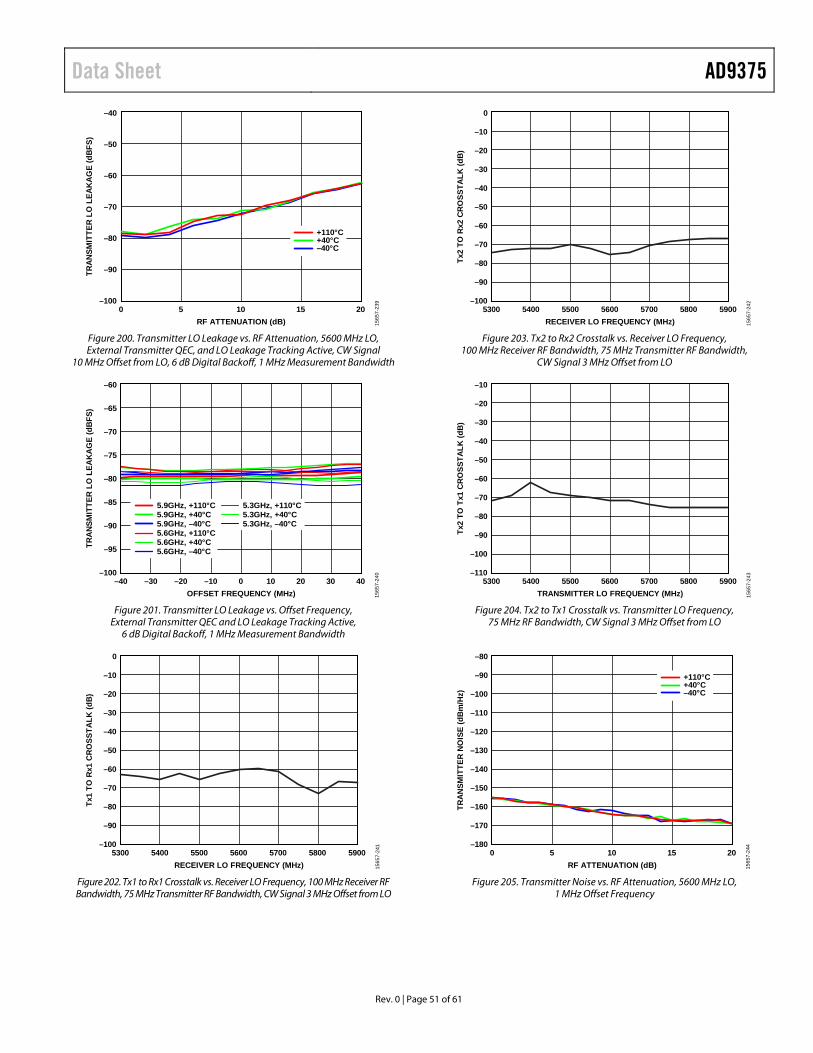
Data Sheet AD9375
Rev. 0 | Page 51 of 61
–40
–1000 20
TRAN
SMIT
TER
LO L
EAKA
GE
(dBF
S)
RF ATTENUATION (dB)
–90
–70
–80
–60
–50
5 10 15
+110°C+40°C–40°C
1565
7-23
9
Figure 200. Transmitter LO Leakage vs. RF Attenuation, 5600 MHz LO, External Transmitter QEC, and LO Leakage Tracking Active, CW Signal
10 MHz Offset from LO, 6 dB Digital Backoff, 1 MHz Measurement Bandwidth
–60
–100–40 40
TRAN
SMIT
TER
LO L
EAKA
GE
(dBF
S)
OFFSET FREQUENCY (MHz)
–90
–75
–80
–95
–85
–70
–65
–20 0 20 30–30 –10 10
5.9GHz, +110°C5.9GHz, +40°C5.9GHz, –40°C5.6GHz, +110°C5.6GHz, +40°C5.6GHz, –40°C
5.3GHz, +110°C5.3GHz, +40°C5.3GHz, –40°C
1565
7-24
0
Figure 201. Transmitter LO Leakage vs. Offset Frequency,
External Transmitter QEC and LO Leakage Tracking Active, 6 dB Digital Backoff, 1 MHz Measurement Bandwidth
0
–1005300 5900
Tx1
TO R
x1 C
RO
SSTA
LK (d
B)
RECEIVER LO FREQUENCY (MHz)
–90
–70
–50
–30
–10
–80
–60
–40
–20
5400 5500 5600 5700 5800
1565
7-24
1
Figure 202. Tx1 to Rx1 Crosstalk vs. Receiver LO Frequency, 100 MHz Receiver RF Bandwidth, 75 MHz Transmitter RF Bandwidth, CW Signal 3 MHz Offset from LO
0
–1005300 5900
Tx2
TO R
x2 C
RO
SSTA
LK (d
B)
RECEIVER LO FREQUENCY (MHz)
–90
–70
–50
–30
–10
–80
–60
–40
–20
5400 5500 5600 5700 5800
1565
7-24
2
Figure 203. Tx2 to Rx2 Crosstalk vs. Receiver LO Frequency,
100 MHz Receiver RF Bandwidth, 75 MHz Transmitter RF Bandwidth, CW Signal 3 MHz Offset from LO
–110
–100
5300 5900
Tx2
TO T
x1 C
RO
SSTA
LK (d
B)
TRANSMITTER LO FREQUENCY (MHz)
–90
–70
–50
–30
–10
–80
–60
–40
–20
5400 5500 5600 5700 5800
1565
7-24
3
Figure 204. Tx2 to Tx1 Crosstalk vs. Transmitter LO Frequency,
75 MHz RF Bandwidth, CW Signal 3 MHz Offset from LO
–80
–1800 20
TRAN
SMIT
TER
NOIS
E (d
Bm/H
z)
RF ATTENUATION (dB)
–170
–140
–160
–120
–100
–130
–150
–110
–90
5 10 15
+110°C+40°C–40°C
1565
7-24
4
Figure 205. Transmitter Noise vs. RF Attenuation, 5600 MHz LO,
1 MHz Offset Frequency
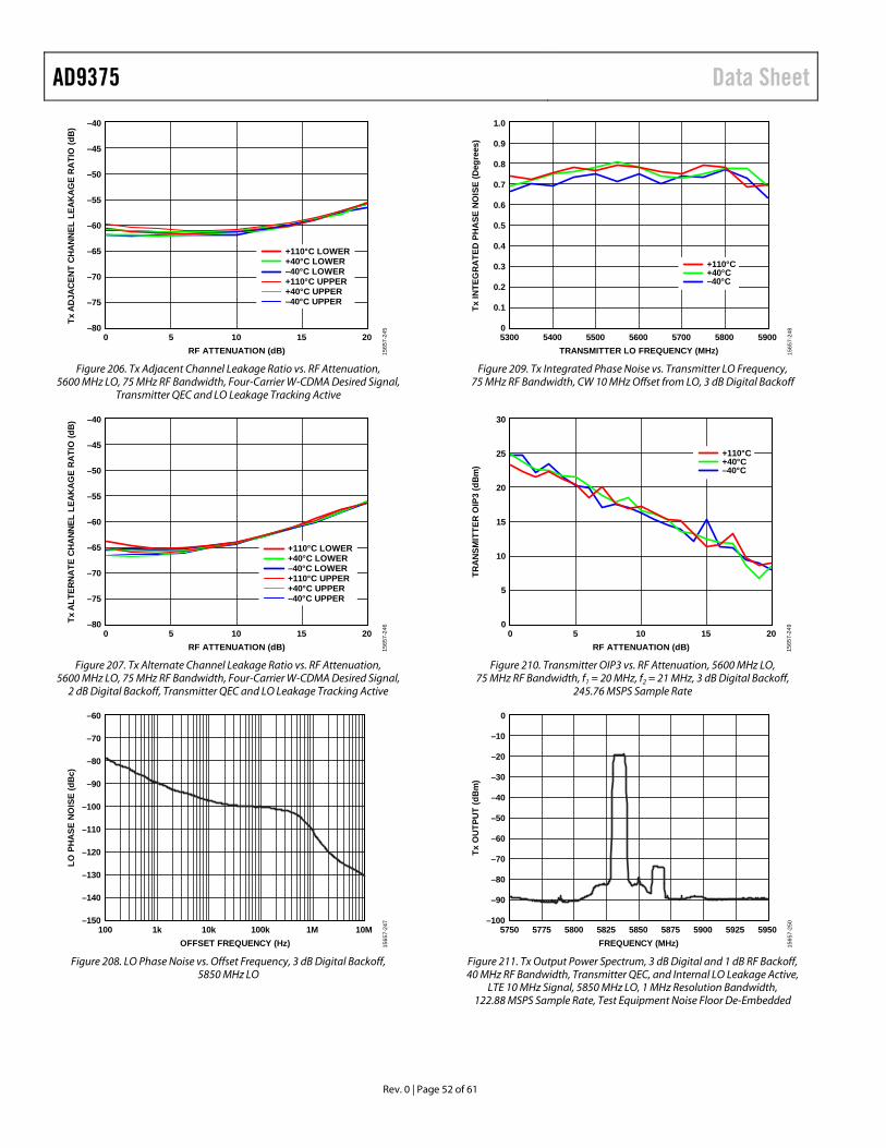
AD9375 Data Sheet
Rev. 0 | Page 52 of 61
–40
–800 20
TxAD
JACE
NT C
HANN
EL L
EAKA
GE
RATI
O (d
B)
RF ATTENUATION (dB)
–70
–60
–50
–65
–75
–55
–45
5 10 15
+110°C LOWER+40°C LOWER–40°C LOWER+110°C UPPER+40°C UPPER–40°C UPPER
1565
7-24
5
Figure 206. Tx Adjacent Channel Leakage Ratio vs. RF Attenuation,
5600 MHz LO, 75 MHz RF Bandwidth, Four-Carrier W-CDMA Desired Signal, Transmitter QEC and LO Leakage Tracking Active
–40
–800 20
TxAL
TERN
ATE
CHAN
NEL
LEAK
AGE
RATI
O (d
B)
RF ATTENUATION (dB)
–70
–60
–50
–65
–75
–55
–45
5 10 15
+110°C LOWER+40°C LOWER–40°C LOWER+110°C UPPER+40°C UPPER–40°C UPPER
1565
7-24
6
Figure 207. Tx Alternate Channel Leakage Ratio vs. RF Attenuation,
5600 MHz LO, 75 MHz RF Bandwidth, Four-Carrier W-CDMA Desired Signal, 2 dB Digital Backoff, Transmitter QEC and LO Leakage Tracking Active
–60
–150100 10M
LO P
HA
SE N
OIS
E (d
Bc)
OFFSET FREQUENCY (Hz)
–120
–100
–80
–110
–140
–130
–90
–70
1k 100k10k 1M
1565
7-24
7
Figure 208. LO Phase Noise vs. Offset Frequency, 3 dB Digital Backoff,
5850 MHz LO
1.0
05300 5900
Tx IN
TEG
RA
TED
PH
ASE
NO
ISE
(Deg
rees
)
TRANSMITTER LO FREQUENCY (MHz)
0.1
0.3
0.5
0.7
0.9
0.2
0.4
0.6
0.8
5400 5500 5600 5700 5800
+110°C+40°C–40°C
1565
7-24
8
Figure 209. Tx Integrated Phase Noise vs. Transmitter LO Frequency,
75 MHz RF Bandwidth, CW 10 MHz Offset from LO, 3 dB Digital Backoff
30
00 20
TRAN
SMIT
TER
OIP
3 (d
Bm)
RF ATTENUATION (dB)
10
20
5
15
25
5 10 15
+110°C+40°C–40°C
1565
7-24
9
Figure 210. Transmitter OIP3 vs. RF Attenuation, 5600 MHz LO,
75 MHz RF Bandwidth, f1 = 20 MHz, f2 = 21 MHz, 3 dB Digital Backoff, 245.76 MSPS Sample Rate
0
–1005750 5950
Tx O
UTP
UT
(dB
m)
FREQUENCY (MHz)
–90
–70
–50
–30
–10
–80
–60
–40
–20
5775 5800 5825 5850 59005875 5925
1565
7-25
0
Figure 211. Tx Output Power Spectrum, 3 dB Digital and 1 dB RF Backoff, 40 MHz RF Bandwidth, Transmitter QEC, and Internal LO Leakage Active,
LTE 10 MHz Signal, 5850 MHz LO, 1 MHz Resolution Bandwidth, 122.88 MSPS Sample Rate, Test Equipment Noise Floor De-Embedded
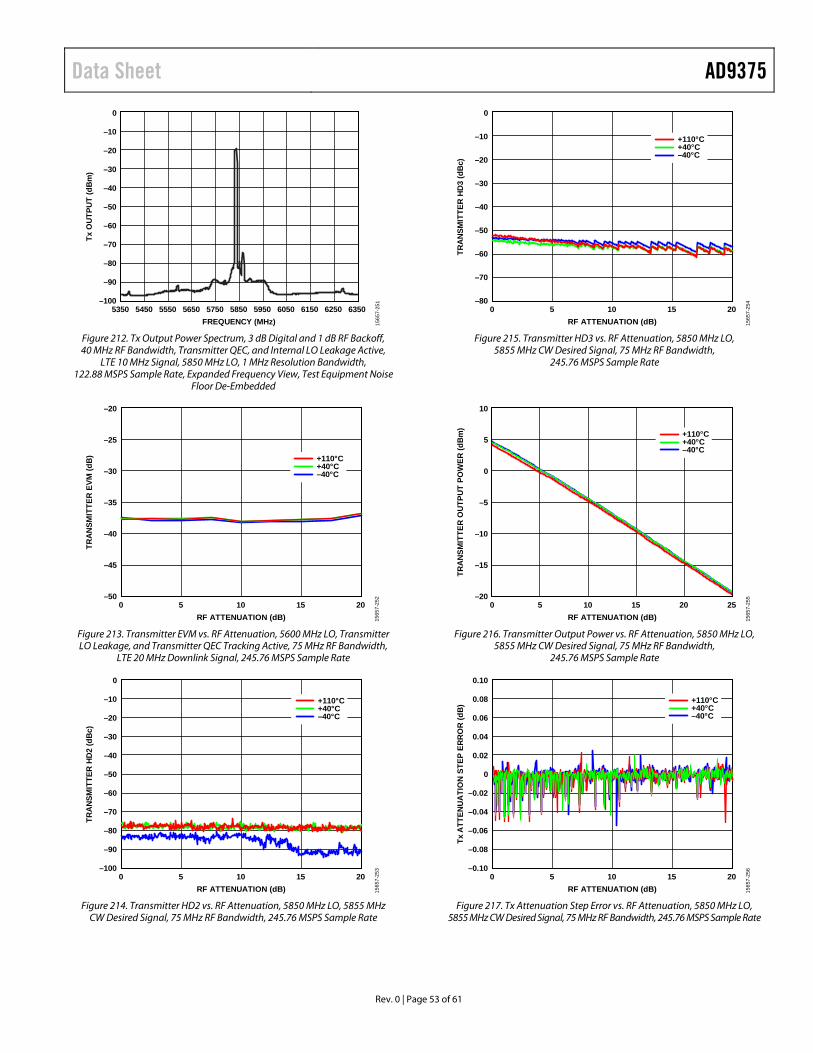
Data Sheet AD9375
Rev. 0 | Page 53 of 61
0
–1005350 6350
Tx O
UTP
UT
(dB
m)
FREQUENCY (MHz)
–90
–70
–50
–30
–10
–80
–60
–40
–20
5450 5550 5650 5750 59505850 61506050 6250
1565
7-25
1
Figure 212. Tx Output Power Spectrum, 3 dB Digital and 1 dB RF Backoff, 40 MHz RF Bandwidth, Transmitter QEC, and Internal LO Leakage Active,
LTE 10 MHz Signal, 5850 MHz LO, 1 MHz Resolution Bandwidth, 122.88 MSPS Sample Rate, Expanded Frequency View, Test Equipment Noise
Floor De-Embedded
–20
–500 20
TRAN
SMIT
TER
EVM
(dB)
RF ATTENUATION (dB)
–45
–35
–40
–30
–25
5 10 15
+110°C+40°C–40°C
1565
7-25
2
Figure 213. Transmitter EVM vs. RF Attenuation, 5600 MHz LO, Transmitter LO Leakage, and Transmitter QEC Tracking Active, 75 MHz RF Bandwidth,
LTE 20 MHz Downlink Signal, 245.76 MSPS Sample Rate
0
–1000 20
TRAN
SMIT
TER
HD2
(dBc
)
RF ATTENUATION (dB)
–70
–80
–90
–60
–30
–50
–10
–40
–20
105 15
+110°C+40°C–40°C
1565
7-25
3
Figure 214. Transmitter HD2 vs. RF Attenuation, 5850 MHz LO, 5855 MHz
CW Desired Signal, 75 MHz RF Bandwidth, 245.76 MSPS Sample Rate
0
–800 20
TRAN
SMIT
TER
HD3
(dBc
)
RF ATTENUATION (dB)
–70
–60
–30
–50
–10
–40
–20
105 15
+110°C+40°C–40°C
1565
7-25
4
Figure 215. Transmitter HD3 vs. RF Attenuation, 5850 MHz LO,
5855 MHz CW Desired Signal, 75 MHz RF Bandwidth, 245.76 MSPS Sample Rate
10
–200 2520
TRAN
SMIT
TER
OUT
PUT
POW
ER (d
Bm)
RF ATTENUATION (dB)
–5
–15
5
–10
0
105 15
+110°C+40°C–40°C
1565
7-25
5
Figure 216. Transmitter Output Power vs. RF Attenuation, 5850 MHz LO,
5855 MHz CW Desired Signal, 75 MHz RF Bandwidth, 245.76 MSPS Sample Rate
0.10
–0.100 20
TxAT
TENU
ATIO
N ST
EP E
RRO
R (d
B)
RF ATTENUATION (dB)
–0.02
–0.04
–0.08
0.08
–0.06
0.02
0.06
0.04
0
105 15
+110°C+40°C–40°C
1565
7-25
6
Figure 217. Tx Attenuation Step Error vs. RF Attenuation, 5850 MHz LO,
5855 MHz CW Desired Signal, 75 MHz RF Bandwidth, 245.76 MSPS Sample Rate
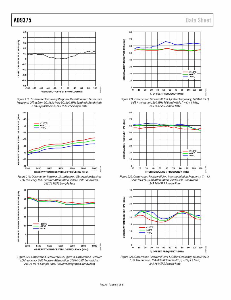
AD9375 Data Sheet
Rev. 0 | Page 54 of 61
0.5
–0.5–100 100
DEV
IATI
ON
FR
OM
FLA
TNES
S (d
B)
FREQUENCY OFFSET FROM LO (MHz)
–0.1
–0.2
–0.4
0.4
–0.3
0.1
0.3
0.2
0
20–40 800–60 60–20–80 40
1565
7-25
7
Figure 218. Transmitter Frequency Response Deviation from Flatness vs. Frequency Offset from LO, 5850 MHz LO, 200 MHz Synthesis Bandwidth,
6 dB Digital Backoff, 245.76 MSPS Sample Rate
–40
–805300 5900
OB
SER
VATI
ON
REC
EIVE
R L
O L
EAK
AG
E (d
Bm
)
OBSERVATION RECEIVER LO FREQUENCY (MHz)
–75
–65
–55
–45
–70
–60
–50
5400 5500 5600 5700 5800
+110°C+40°C–40°C
1565
7-25
8
Figure 219. Observation Receiver LO Leakage vs. Observation Receiver
LO Frequency, 0 dB Receiver Attenuation, 200 MHz RF Bandwidth, 245.76 MSPS Sample Rate
30
05300 5900
OB
SER
VATI
ON
REC
EIVE
R N
OIS
E FI
GU
RE
(dB
)
OBSERVATION RECEIVER LO FREQUENCY (MHz)
5
15
25
10
20
5400 5500 5600 5700 5800
+110°C+40°C–40°C
1565
7-25
9
Figure 220. Observation Receiver Noise Figure vs. Observation Receiver LO Frequency, 0 dB Receiver Attenuation, 200 MHz RF Bandwidth,
245.76 MSPS Sample Rate, 100 MHz Integration Bandwidth
80
00 10 110
OB
SER
VATI
ON
REC
EIVE
R II
P2 (d
Bm
)
f1 OFFSET FREQUENCY (MHz)
10
30
70
20
50
60
40
20 40 60 8030 50 70 90 100
+110°C+40°C–40°C
1565
7-22
1
Figure 221. Observation Receiver IIP2 vs. f1 Offset Frequency, 5600 MHz LO,
0 dB Attenuation, 200 MHz RF Bandwidth, f2 = f1 + 1 MHz, 245.76 MSPS Sample Rate
80
010 110
OB
SER
VATI
ON
REC
EIVE
R II
P2 (d
Bm
)
INTERMODULATION FREQUENCY (MHz)
10
30
70
20
50
60
40
20 40 60 8030 50 70 90 100
+110°C+40°C–40°C
1565
7-26
0
Figure 222. Observation Receiver IIP2 vs. Intermodulation Frequency (f2 − f1),
5600 MHz LO, 0 dB Attenuation, 200 MHz RF Bandwidth, 245.76 MSPS Sample Rate
40
35
30
25
20
15
10
5
00 110100908070605040302010
OB
SER
VATI
ON
REC
EIVE
R II
P3 (d
Bm
)
f1 OFFSET FREQUENCY (MHz)
+110°C+40°C–40°C
1565
7-22
2
Figure 223. Observation Receiver IIP3 vs. f1 Offset Frequency, 5600 MHz LO,
0 dB Attenuation, 200 MHz RF Bandwidth, f2 = 2 f1 + 1 MHz, 245.76 MSPS Sample Rate
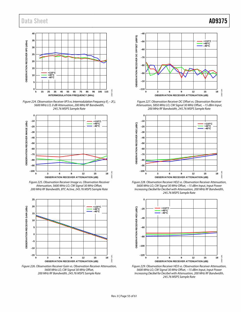
Data Sheet AD9375
Rev. 0 | Page 55 of 61
40
05 115
OB
SER
VATI
ON
REC
EIVE
R II
P3 (d
Bm
)
INTERMODULATION FREQUENCY (MHz)
5
15
35
10
25
30
20
15 35 55 7525 45 65 85 95 105
+110°C+40°C–40°C
1565
7-26
1
Figure 224. Observation Receiver IIP3 vs. Intermodulation Frequency (f2 − 2f1), 5600 MHz LO, 0 dB Attenuation, 200 MHz RF Bandwidth,
245.76 MSPS Sample Rate
0
–1000 18
OBS
ERVA
TIO
N RE
CEIV
ER IM
AGE
(dBc
)
OBSERVATION RECEIVER ATTENUATION (dB)
–70
–80
–90
–60
–30
–50
–10
–40
–20
63 129 15
+110°C+40°C–40°C
1565
7-26
2
Figure 225. Observation Receiver Image vs. Observation Receiver
Attenuation, 5600 MHz LO, CW Signal 30 MHz Offset, 200 MHz RF Bandwidth, BTC Active, 245.76 MSPS Sample Rate
25
–150 18
OBS
ERVA
TIO
N RE
CEIV
ER G
AIN
(dBc
)
OBSERVATION RECEIVER ATTENUATION (dB)
–10
–5
10
0
20
5
15
63 129 15
+110°C+40°C–40°C
1565
7-26
3
Figure 226. Observation Receiver Gain vs. Observation Receiver Attenuation,
5600 MHz LO, CW Signal 30 MHz Offset, 200 MHz RF Bandwidth, 245.76 MSPS Sample Rate
–40
–50
–60
–70
–80
–90
–10
–1100 181512963
OBS
ERVA
TIO
N RE
CEIV
ER D
C O
FFSE
T (d
BFS)
OBSERVATION RECEIVER ATTENUATION (dB)
+110°C+40°C–40°C
1565
7-26
4
Figure 227. Observation Receiver DC Offset vs. Observation Receiver Attenuation, 5850 MHz LO, CW Signal 30 MHz Offset, −15 dBm Input,
200 MHz RF Bandwidth, 245.76 MSPS Sample Rate
0
–1000 18
OBS
ERVA
TIO
N RE
CEIV
ER H
D2 (d
BC)
OBSERVATION RECEIVER ATTENUATION (dB)
–90
–80
–70
–50
–30
–10
–60
–40
–20
63 129 15
+110°C+40°C–40°C
1565
7-26
5
Figure 228. Observation Receiver HD2 vs. Observation Receiver Attenuation,
5600 MHz LO, CW Signal 30 MHz Offset, −15 dBm Input, Input Power Increasing Decibel for Decibel with Attenuation, 200 MHz RF Bandwidth,
245.76 MSPS Sample Rate
0
–120
–100
0 18
OBS
ERVA
TIO
N RE
CEIV
ER H
D3 (d
BC)
OBSERVATION RECEIVER ATTENUATION (dB)
–80
–60
–40
–20
63 129 15
+110°C+40°C–40°C
1565
7-26
6
Figure 229. Observation Receiver HD3 vs. Observation Receiver Attenuation,
5600 MHz LO, CW Signal 30 MHz Offset, −15 dBm Input, Input Power Increasing Decibel for Decibel with Attenuation, 200 MHz RF Bandwidth,
245.76 MSPS Sample Rate
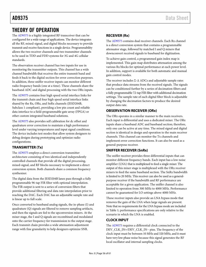
AD9375 Data Sheet
Rev. 0 | Page 56 of 61
THEORY OF OPERATION The AD9375 is a highly integrated RF transceiver that can be configured for a wide range of applications. The device integrates all the RF, mixed-signal, and digital blocks necessary to provide transmit and receive functions in a single device. Programmability allows the two receiver channels and two transmitter channels to be used in TDD and FDD systems for 3G and 4G cellular standards.
The observation receiver channel has two inputs for use in monitoring the transmitter outputs. This channel has a wide channel bandwidth that receives the entire transmit band and feeds it back to the digital section for error correction purposes. In addition, three sniffer receiver inputs can monitor different radio frequency bands (one at a time). These channels share the baseband ADC and digital processing with the two ORx inputs.
The AD9375 contains four high speed serial interface links for the transmit chain and four high speed serial interface links shared by the Rx, ORx, and SnRx channels (JESD204B, Subclass 1 compliant), providing a low pin count and reliable data interface to a field-programmable gate array (FPGA) or other custom integrated baseband solutions.
The AD9375 also provides self calibration for dc offset and quadrature error correction to maintain a high performance level under varying temperatures and input signal conditions. The device includes test modes that allow system designers to debug designs during prototyping and optimize radio configurations.
TRANSMITTER (Tx) The AD9375 employs a direct conversion transmitter architecture consisting of two identical and independently controlled channels that provide all the digital processing, mixed-signal, and RF blocks necessary to implement a direct conversion system. Both channels share a common frequency synthesizer.
The digital data from the JESD204B lanes pass through a fully programmable 96-tap FIR filter with optional interpolation. The FIR output is sent to a series of conversion filters that provide additional filtering and data rate interpolation prior to reaching the DAC. Each DAC has an adjustable sample rate and is linear up to full scale.
Once converted to baseband analog signals, the in-phase (I) and quadrature (Q) signals are filtered to remove sampling artifacts, and then the signals are fed to the upconversion mixers. At the mixer stage, the I and Q signals are recombined and modulated onto the carrier frequency for transmission to the output stage. Each transmit chain provides a wide attenuation adjustment range with fine granularity to help designers optimize SNR.
RECEIVER (Rx) The AD9375 contains dual receiver channels. Each Rx channel is a direct conversion system that contains a programmable attenuator stage, followed by matched I and Q mixers that downconvert received signals to baseband for digitization.
To achieve gain control, a programmed gain index map is implemented. This gain map distributes attenuation among the various Rx blocks for optimal performance at each power level. In addition, support is available for both automatic and manual gain control modes.
The receiver includes Σ-Δ ADCs and adjustable sample rates that produce data streams from the received signals. The signals can be conditioned further by a series of decimation filters and a fully programmable 72-tap FIR filter with additional decimation settings. The sample rate of each digital filter block is adjustable by changing the decimation factors to produce the desired output data rate.
OBSERVATION RECEIVER (ORx) The ORx operates in a similar manner to the main receivers. Each input is differential and uses a dedicated mixer. The ORx inputs share a baseband ADC and baseband section; therefore, only one can be active at any time. The mixed signal and digital section is identical in design and operation to the main receiver channels. This channel can monitor the Tx channels and implement error correction functions. It can also be used as a general-purpose receiver.
SNIFFER RECEIVER (SnRx) The sniffer receiver provides three differential inputs that can monitor different frequency bands. Each input has a low noise amplifier (LNA) that is multiplexed to feed a single mixer. The output of this mixer stage is multiplexed with the ORx receiver mixers to feed the same baseband section. The SnRx bandwidth is limited to 20 MHz. This receiver can also be used as a general-purpose receiver if the bandwidth and RF performance are acceptable for a given application. The sniffer channel is also limited to operation from 300 MHz to 4000 MHz. Performance cannot be guaranteed for LO settings above 4000 MHz.
These receiver inputs also provide an LNA bypass mode that removes the gain of the LNA when large signals are present. Note that no requirements for the LNA bypass mode are included in Table 1; performance specifications are only relative to the scenario in which the LNA is enabled.
CLOCK INPUT The AD9375 requires a differential clock connected to the DEV_CLK_IN+/DEV_CLK_IN− pins. The frequency of the clock input must be between 10 MHz and 320 MHz, and it must have very low phase noise because this signal generates the RF local oscillator and internal sampling clocks.
Data Sheet AD9375
Rev. 0 | Page 57 of 61
SYNTHESIZERS RF PLL
The AD9375 contains three fractional-N PLLs to generate the RF LOs used by the transmitter, receiver, and observation receiver. The PLL incorporates an internal VCO and loop filter that require no external components. The internal VCO LDO regulators eliminate the need for additional external power supplies for the PLLs. These regulators only require an external bypass capacitor for each supply.
Clock PLL
The AD9375 contains a PLL synthesizer that generates all of the baseband related clock signals and SERDES clocks. This PLL is programmed based on the data rate and sample rate requirements of the system.
SERIAL PERIPHERAL INTERFACE (SPI) The AD9375 uses a SPI to communicate with the baseband processor (BBP). This interface can be configured as a 4-wire interface with dedicated receive and transmit ports, or it can be configured as a 3-wire interface with a bidirectional data communications port. This bus allows the BBP to set all device control parameters using a simple address data serial bus protocol.
Write commands follow a 24-bit format. The first bit sets the bus direction of the bus transfer. The next 15 bits set the address where data is written. The final eight bits are the data being transferred to the specific register address.
Read commands follow a similar format with the exception that the first 16 bits are transferred on the SDIO pin, and the final eight bits are read from the AD9375, either on the SDO pin in 4-wire mode or on the SDIO pin in 3-wire mode.
GPIO_x AND GPIO_3P3_x PINS The AD9375 general-purpose input/output signals referenced to the VDD_IF supply can be configured for numerous functions. Some of these pins, when configured as outputs, are used by the BBP as real-time signals to provide a number of internal settings and measurements. This configuration allows the BBP to monitor receiver performance in different situations. A pointer register selects the information that is output to these pins. Signals used for manual gain mode, calibration flags, state machine states, and various receiver parameters are among the outputs that can be monitored on these pins. In addition, certain pins can be configured as inputs and used in various functions such as setting the receiver gain in real time.
The GPIO_3P3_x pins are referenced to the VDDA_3P3 supply. These pins can provide control signals to other components such as voltage gain amplifiers (VGAs) or attenuators in the RF section that typically use a higher reference voltage.
AUXILIARY CONVERTERS Auxiliary ADC Inputs (AUXADC_x)
The AD9375 contains an auxiliary ADC that is multiplexed to four input pins (AUXADC_0 through AUXADC_3). This block can monitor system voltages without adding additional components. The auxiliary ADC is 12 bits with an input voltage range of 0.05 V to VDDA_3P3 − 0.05 V. When enabled, the auxiliary ADC is free running. Software reads of the output value provide the last value latched at the ADC output.
Auxiliary DACs (AUXDAC_x)
The AD9375 contains 10 identical auxiliary DACs (AUXDAC_0 to AUXDAC_9) that can supply bias voltages, analog control voltages, or other system functionality. The inputs of these auxiliary DACs (AUXDAC_0 to AUXDAC_9) are multiplexed with the GPIO_ 3P3_x pins according to Table 7. The auxiliary DACs are 10 bits, have an output voltage range of approximately 0.5 V to 3.0 V, and have a current drive of 10 mA.
Table 7. AUXDAC Input Pin Assignments AUXDAC_x Output GPIO_3P3_x Pin AUXDAC_0 GPIO_3P3_9 AUXDAC_1 GPIO_3P3_7 AUXDAC_2 GPIO_3P3_6 AUXDAC_3 GPIO_3P3_10 AUXDAC_4 GPIO_3P3_0 AUXDAC_5 GPIO_3P3_1 AUXDAC_6 GPIO_3P3_3 AUXDAC_7 GPIO_3P3_4 AUXDAC_8 GPIO_3P3_5 AUXDAC_9 GPIO_3P3_8
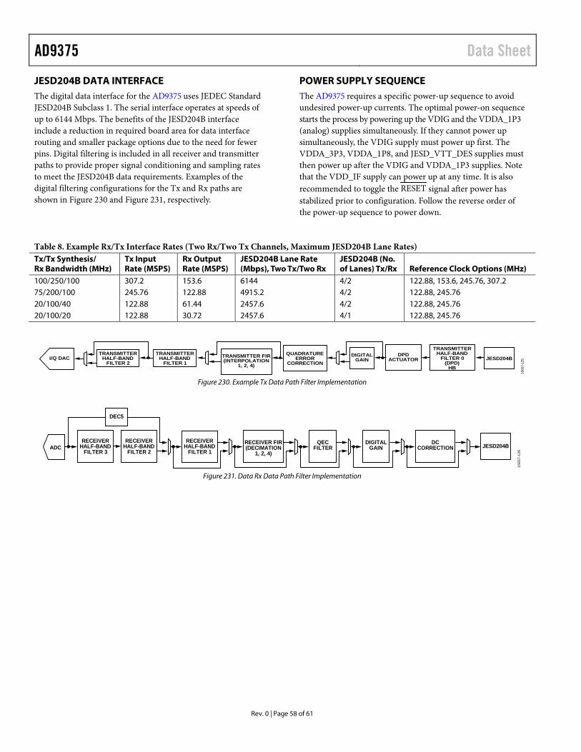
AD9375 Data Sheet
Rev. 0 | Page 58 of 61
JESD204B DATA INTERFACE The digital data interface for the AD9375 uses JEDEC Standard JESD204B Subclass 1. The serial interface operates at speeds of up to 6144 Mbps. The benefits of the JESD204B interface include a reduction in required board area for data interface routing and smaller package options due to the need for fewer pins. Digital filtering is included in all receiver and transmitter paths to provide proper signal conditioning and sampling rates to meet the JESD204B data requirements. Examples of the digital filtering configurations for the Tx and Rx paths are shown in Figure 230 and Figure 231, respectively.
POWER SUPPLY SEQUENCE The AD9375 requires a specific power-up sequence to avoid undesired power-up currents. The optimal power-on sequence starts the process by powering up the VDIG and the VDDA_1P3 (analog) supplies simultaneously. If they cannot power up simultaneously, the VDIG supply must power up first. The VDDA_3P3, VDDA_1P8, and JESD_VTT_DES supplies must then power up after the VDIG and VDDA_1P3 supplies. Note that the VDD_IF supply can power up at any time. It is also recommended to toggle the RESET signal after power has stabilized prior to configuration. Follow the reverse order of the power-up sequence to power down.
Table 8. Example Rx/Tx Interface Rates (Two Rx/Two Tx Channels, Maximum JESD204B Lane Rates) Tx/Tx Synthesis/ Rx Bandwidth (MHz)
Tx Input Rate (MSPS)
Rx Output Rate (MSPS)
JESD204B Lane Rate (Mbps), Two Tx/Two Rx
JESD204B (No. of Lanes) Tx/Rx Reference Clock Options (MHz)
100/250/100 307.2 153.6 6144 4/2 122.88, 153.6, 245.76, 307.2 75/200/100 245.76 122.88 4915.2 4/2 122.88, 245.76 20/100/40 122.88 61.44 2457.6 4/2 122.88, 245.76 20/100/20 122.88 30.72 2457.6 4/1 122.88, 245.76
I/Q DAC TRANSMITTER FIR(INTERPOLATION
1, 2, 4)
DIGITALGAIN JESD204B
QUADRATUREERROR
CORRECTION
DPDACTUATOR
TRANSMITTERHALF-BAND
FILTER 0(DPD)
HB
1565
7-12
5
TRANSMITTERHALF-BAND
FILTER 2
TRANSMITTERHALF-BAND
FILTER 1
Figure 230. Example Tx Data Path Filter Implementation
ADC JESD204BRECEIVER
HALF-BANDFILTER 3
RECEIVER FIR(DECIMATION
1, 2, 4)
QECFILTER
DCCORRECTION
DIGITALGAIN
DEC5
RECEIVERHALF-BAND
FILTER 2
RECEIVERHALF-BAND
FILTER 1
1565
7-12
6
Figure 231. Data Rx Data Path Filter Implementation
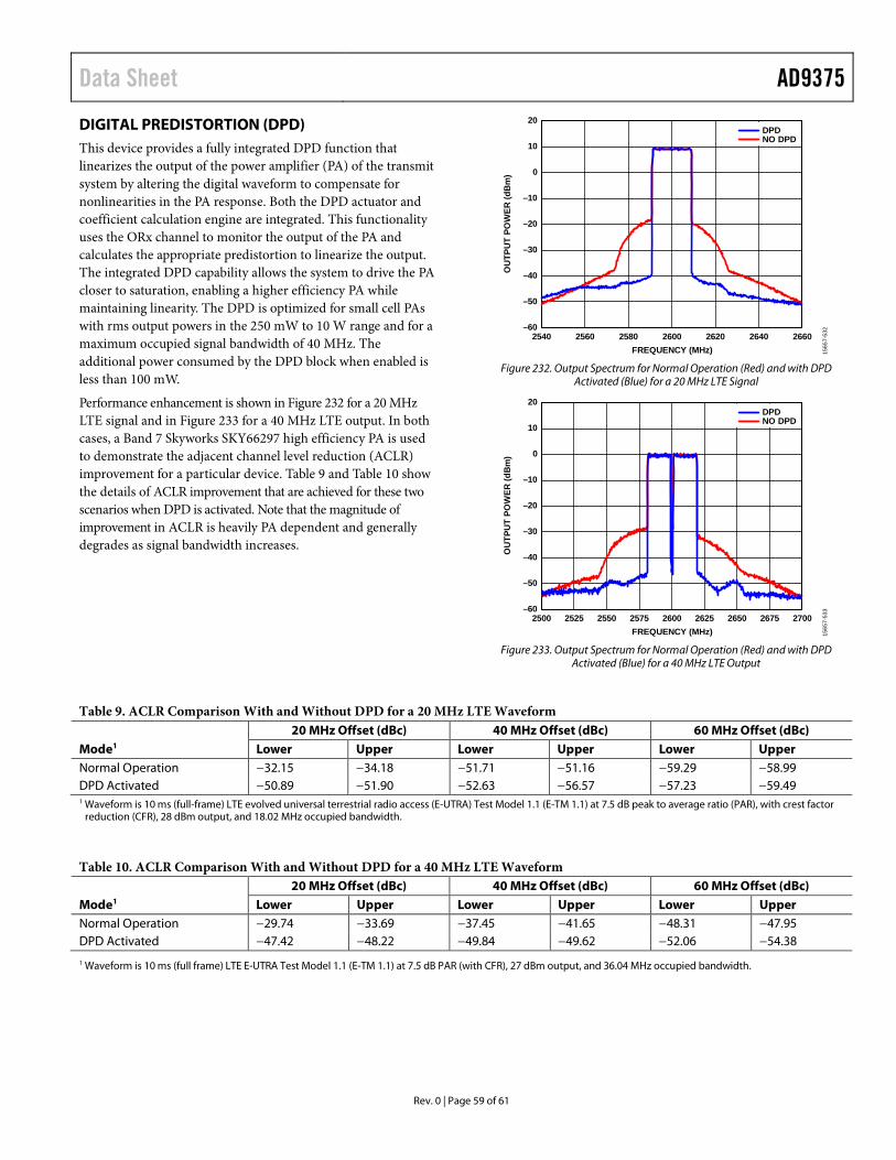
Data Sheet AD9375
Rev. 0 | Page 59 of 61
DIGITAL PREDISTORTION (DPD) This device provides a fully integrated DPD function that linearizes the output of the power amplifier (PA) of the transmit system by altering the digital waveform to compensate for nonlinearities in the PA response. Both the DPD actuator and coefficient calculation engine are integrated. This functionality uses the ORx channel to monitor the output of the PA and calculates the appropriate predistortion to linearize the output. The integrated DPD capability allows the system to drive the PA closer to saturation, enabling a higher efficiency PA while maintaining linearity. The DPD is optimized for small cell PAs with rms output powers in the 250 mW to 10 W range and for a maximum occupied signal bandwidth of 40 MHz. The additional power consumed by the DPD block when enabled is less than 100 mW.
Performance enhancement is shown in Figure 232 for a 20 MHz LTE signal and in Figure 233 for a 40 MHz LTE output. In both cases, a Band 7 Skyworks SKY66297 high efficiency PA is used to demonstrate the adjacent channel level reduction (ACLR) improvement for a particular device. Table 9 and Table 10 show the details of ACLR improvement that are achieved for these two scenarios when DPD is activated. Note that the magnitude of improvement in ACLR is heavily PA dependent and generally degrades as signal bandwidth increases.
20
–60
–50
–40
–30
–20
–10
0
10
2540 2560 2580 2600 2620 2640 2660
OU
TPU
T PO
WER
(dB
m)
FREQUENCY (MHz)
DPDNO DPD
1565
7-53
2
Figure 232. Output Spectrum for Normal Operation (Red) and with DPD
Activated (Blue) for a 20 MHz LTE Signal
20
–60
–50
–40
–30
–20
–10
0
10
2500 2525 2550 2575 2600 2625 2650 2675 2700
OU
TPU
T PO
WER
(dB
m)
FREQUENCY (MHz)
DPDNO DPD
1565
7-53
3
Figure 233. Output Spectrum for Normal Operation (Red) and with DPD
Activated (Blue) for a 40 MHz LTE Output
Table 9. ACLR Comparison With and Without DPD for a 20 MHz LTE Waveform
Mode1 20 MHz Offset (dBc) 40 MHz Offset (dBc) 60 MHz Offset (dBc)
Lower Upper Lower Upper Lower Upper Normal Operation −32.15 −34.18 −51.71 −51.16 −59.29 −58.99 DPD Activated −50.89 −51.90 −52.63 −56.57 −57.23 −59.49 1 Waveform is 10 ms (full-frame) LTE evolved universal terrestrial radio access (E-UTRA) Test Model 1.1 (E-TM 1.1) at 7.5 dB peak to average ratio (PAR), with crest factor
reduction (CFR), 28 dBm output, and 18.02 MHz occupied bandwidth.
Table 10. ACLR Comparison With and Without DPD for a 40 MHz LTE Waveform
Mode1 20 MHz Offset (dBc) 40 MHz Offset (dBc) 60 MHz Offset (dBc)
Lower Upper Lower Upper Lower Upper Normal Operation −29.74 −33.69 −37.45 −41.65 −48.31 −47.95 DPD Activated −47.42 −48.22 −49.84 −49.62 −52.06 −54.38
1 Waveform is 10 ms (full frame) LTE E-UTRA Test Model 1.1 (E-TM 1.1) at 7.5 dB PAR (with CFR), 27 dBm output, and 36.04 MHz occupied bandwidth.
AD9375 Data Sheet
Rev. 0 | Page 60 of 61
JTAG BOUNDARY SCAN The AD9375 provides support for a JTAG boundary scan. Five dual-function pins are associated with the JTAG interface. These pins, listed in Table 11, are used to access the on-chip test access port. To enable the JTAG functionality, set the GPIO_0 through GPIO_3 pins according to Table 12 depending on how the desired JESD204B sync pin (that is, SYNCINB0+, SYNCINB0−, SYNCINB1+, SYNCINB1−, SYNCOUTB0+, or SYNCOUTB0−) is configured in the software (LVDS or CMOS mode). Pull the TEST pin high to enable the JTAG mode.
Table 11. Dual-Function Boundary Scan Test Pins Mnemonic JTAG Mnemonic Description GPIO_4 TRST Test access port reset
GPIO_5 TDO Test data output GPIO_6 TDI Test data input GPIO_7 TMS Test access port mode select GPIO_18 TCK Test clock
Table 12. JTAG Modes Test Pin Level GPIO_0 to GPIO_3 Description 0 XXXX1 Normal operation 1 1001 JTAG mode with LVDS
JESD204B sync signals 1 1011 JTAG mode with CMOS
JESD204B sync signals
1 X means don’t care.
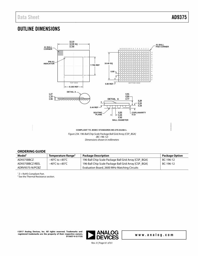
Data Sheet AD9375
Rev. 0 | Page 61 of 61
OUTLINE DIMENSIONS
COMPLIANT TO JEDEC STANDARDS MO-275-GGAB-1. 03-0
2-20
15-A
0.80
0.80 REF
0.44 REF
ABCDEFG
91011121314 8 7 56 4 23 1
BOTTOM VIEW
10.40 SQ
HJKLMNP
DETAIL A
TOP VIEW
DETAIL A
COPLANARITY0.12
0.500.450.40
BALL DIAMETER
SEATINGPLANE
12.1012.00 SQ11.90
A1 BALLPAD CORNER
1.271.181.09
7.755 REF
8.165 REF
0.910.840.77
0.390.340.29
PKG
-004
569
A1 BALLCORNER
PIN A1INDICATOR
Figure 234. 196-Ball Chip Scale Package Ball Grid Array [CSP_BGA]
(BC-196-12) Dimensions shown in millimeters
ORDERING GUIDE Model1 Temperature Range2 Package Description Package Option AD9375BBCZ −40°C to +85°C 196-Ball Chip Scale Package Ball Grid Array [CSP_BGA] BC-196-12 AD9375BBCZ-REEL −40°C to +85°C 196-Ball Chip Scale Package Ball Grid Array [CSP_BGA] BC-196-12 ADRV9375-N/PCBZ Evaluation Board, 2600 MHz Matching Circuits 1 Z = RoHS-Compliant Part. 2 See the Thermal Resistance section.
©2017 Analog Devices, Inc. All rights reserved. Trademarks and registered trademarks are the property of their respective owners. D15657-0-3/17(0)
Recommended