Ken Goodson
Professor & Vice Chair
Mechanical Engineering
Stanford University
Nano Thermal Management
for Electronics MEPTEC 2012
March 19, 2012
Intel/Numonyx Vuckovic Group, Stanford
http://www.nanoheat.stanford.edu
Micro hx
EO Pump
Heatrejector
Micro hx
EO Pump
Heatrejector

Electronics Thermal Challenges
portables
servers
transportation defense
energy efficiency
hotspot mitigation
heterogeneous
integration

portables
servers
transportation defense
Electronics Thermal Challenges

portables
servers
transportation defense
Electronics Thermal Challenges

Energy
Efficiency
Performance
nonvolatile memory
Our Research
RF electronics
3D integration
optical
interconnects
rapid PCR &
blood analysis
thermoelectric
harvesting
heat & power for
computation
heat & power in
portables

PCRAM Data Storage
Thermal
Interfaces nanoThermo-
electrics
with RTI
EUV Nano
Mirrors
Goodson group & Monano
collaborators, Stanford
with Group4 Labs
Composite
Substrates
with Intel TMG
with KLA Tencor
with Vuckovic et al.
Stanford
QC Lasers/Guides
Micro HX
Membranes
Milnes David,
Goodson group, Stanford
Liquid region
vapor
AlGaN
Diamond
NanoMaterials

Non uniform heat generating chip
Base
IR transparent window
Imaging lens
To detector
IR radiation
IR transparent fluid
(a)
1
3
5
1
4
2
7
8
9 6
15
13 ,14
10 11 12
16
• Real-time power and hotspot
mapping for temp/power–aware
computing and energy saving.
• Microfluidic cooling including
Porous Membrane Vapor Venting
and 3D in-situ extraction (MCCI)
•Nanostructured underfill and
thermal interface materials (TIM)
•Low-power nonvolatile memory
technologies including PCRAM
0
5
10
15
20
25
-0.2 0 0.2 0.4 0.6 0.8 1
Exit Quality
No
rm P
ress
ure
[P
/P li
q]
vent
2ml/min
Con
vent
iona
l
(a)
(b)
PMVV
Technology
(a) (b) (c) Distributed
Temperature
Sensor
Network
Rep
rod
uced
po
wer
map
Po
wer
map
Rapid Hotspot Prediction & Power Distribution
Advanced Vapor Chambers
Microfluidic Cooling
Lid/SpreaderThermal
Block
Nanostructured Underfill and Interface Materials
Silicon Nanopillar Hydrophilic Layer
Heat & Power Management
for Computation
Through-Wafer
Hotspot Imaging
http://www.stanford.edu/group/microheat/
Nonvolatile Memory
including PCRAM
GS
T
GS
T

Selected Alumni
Prof. Dan Fletcher UC Berkeley Dr. Jeremy Rowlette Daylight Solns
Prof. Evelyn Wang MIT Dr. Patricia Gharagozloo Sandia Labs
Prof. Katsuo Kurabayashi U. Michigan Dr. Per Sverdrup Intel
Prof. Sungtaek Ju UCLA Dr. Chen Fang Exxon-Mobile
Prof. Mehdi Asheghi Stanford Dr. Milnes David IBM
Prof. Bill King UIUC Dr. Max Touzelbaev AMD
Prof. Eric Pop UIUC (EE) Dr. Roger Flynn Intel
Prof. Sanjiv Sinha UIUC Dr. Julie Steinbrenner Xerox Parc
Prof. Xeujiao Hu Wuhan Univ. Dr. John Reifenberg Intel
Prof. Carlos Hidrovo UT Austin Dr. David Fogg Creare
Prof. Kaustav Banerjee UCSB (EE) Dr. Matthew Panzer KLA-Tencor
Prof. Ankur Jain UT Arlington
Prof. Sarah Parikh Foothill College
Current Group Ken Goodson
Josef Miler Elah Bozorg-Grayeli Lewis Hom
Michael Barako Amy Marconnet Aditja Sood (MSE)
Jaeho Lee Shilpi Roy (EE) Woosung Parc
Sri Lingamneni Yuan Gao
Saniya Leblanc Yiyang Li (MSE) Dr. Takashi Kodama
Jungwan Cho Zijian Li Dr. Yoonjin Won
Prof. Mehdi Asheghi

Outline
Metrology
GaN-Diamond HEMTs
Phase Change Memory
3D NanoPackaging
Microfluidic Cooling
http://www.nanoheat.stanford.edu

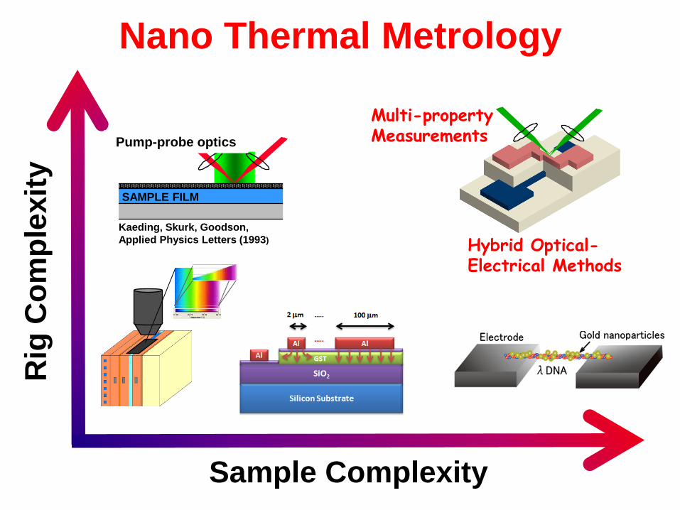
Sample Complexity
Rig
Co
mp
lexit
y
Kodama, Jain, Goodson, Nano Letters 9 (2009)
Nano Thermal Metrology

Nanobridge Samples
ALD Pt
SiO2
Si
10 nm
Free-standing
WFL
Bulk
Thermal conductivity (W/mK)
Bridge Thickness (nm)
SiO2 Si3N4
nanotube Pt
Pt gate
2 μm nanotube on
substrate suspended
over trench
0 0.2 0.4 0.6 0.8 1 1.20
2
4
6
8
10
12
14
16
I (
A)
V (V)
On Substrate
Suspended
L = 3 m
Cu
rren
t (
A)
Voltage (V)
On substrate
Suspended
Single Wall Carbon Nanotube FETs Pop, Dai, Goodson, et al., Physical Review Letters (2005), Nano Letters (2006)
Metal Interconnects down to 7.3 nm Students: Yoneoka & Lee, Nano Letters (2012, in press)

Sample Complexity
Rig
Co
mp
lexit
y
Kodama, Jain, Goodson, Nano Letters 9 (2009)
Nano Thermal Metrology

Sample Complexity
Rig
Co
mp
lexit
y
Nano Thermal Metrology
Kodama, Jain, Goodson, Nano Letters 9 (2009)
Marconnet, Wardle, Goodson, et al., ACS Nano (2011)
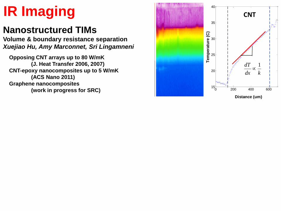
IR Imaging Heater
growth substrate
CNT Film
0 200 400 60015
20
25
30
35
40
Distance (um)
Tem
pera
ture
(C
)
CNT
kdx
dT 1
Nanostructured TIMs Volume & boundary resistance separation
Xuejiao Hu, Amy Marconnet, Sri Lingamneni
Opposing CNT arrays up to 80 W/mK
(J. Heat Transfer 2006, 2007)
CNT-epoxy nanocomposites up to 5 W/mK
(ACS Nano 2011)
Graphene nanocomposites
(work in progress for SRC)

IR Imaging
Nanostructured TIMs Volume & boundary resistance separation
Xuejiao Hu, Amy Marconnet, Sri Lingamneni
Opposing CNT arrays up to 80 W/mK
(J. Heat Transfer 2006, 2007)
CNT-epoxy nanocomposites up to 5 W/mK
(ACS Nano 2011)
Graphene nanocomposites
(work in progress for SRC)
IR Solid Immersion Lens Submicron resolution with microcantilever
Daniel Fletcher
First thermal microscopy demonstration
(Microscale Thermophysical Engineering 2003)
Electromagnetic simulations and optimization
(Optics Letters 2001)
Microfabrication details
(J. MicroElectroMechanical Systems 2001)
Resolution demonstration
(Applied Physics Letters 2000)
10 µm
silicon
tip
pyrex

Sample Complexity
Rig
Co
mp
lexit
y
Nano Thermal Metrology
Kodama, Jain, Goodson, Nano Letters 9 (2009)
Marconnet, Wardle, Goodson, et al., ACS Nano (2011)

Sample Complexity
Rig
Co
mp
lexit
y
SAMPLE FILM
Kaeding, Skurk, Goodson,
Applied Physics Letters (1993)
Pump-probe optics
Nano Thermal Metrology
Kodama, Jain, Goodson, Nano Letters 9 (2009)
Marconnet, Wardle, Goodson, et al., ACS Nano (2011)
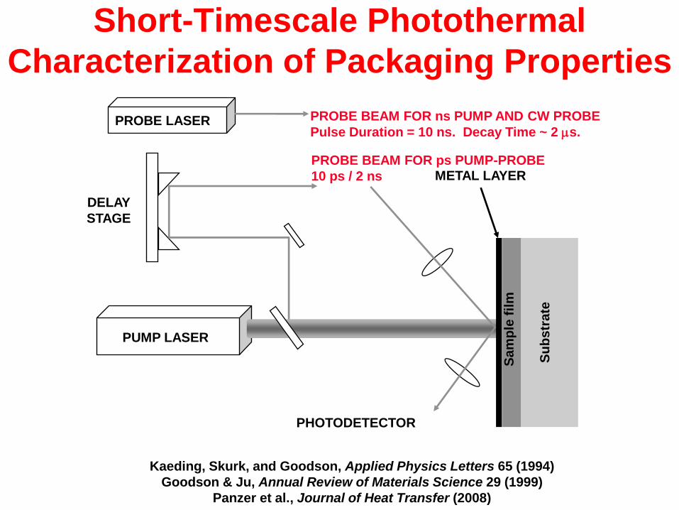
Kaeding, Skurk, and Goodson, Applied Physics Letters 65 (1994)
Goodson & Ju, Annual Review of Materials Science 29 (1999)
Panzer et al., Journal of Heat Transfer (2008)
DELAY
STAGE
PUMP LASER
PROBE BEAM FOR ns PUMP AND CW PROBE
Pulse Duration = 10 ns. Decay Time ~ 2 s. PROBE LASER
PHOTODETECTOR
METAL LAYER PROBE BEAM FOR ps PUMP-PROBE
10 ps / 2 ns
Short-Timescale Photothermal
Characterization of Packaging Properties
Sa
mp
le f
ilm
Su
bs
tra
te

Applications
Thermal Interface
Metal
Metal Catalyst
Transparent
Substrate
Die Attach
Distributions
Matt Panzer, Yuan Gao,
Amy Marconnet
Nanoletters (2010)
J. Heat Transfer (2008)
J. Electronic Materials (2009)
Intel Proprietary Layers
Alloy TIM
Si
Interconnects &
Low-K Dielectrics AlCu on polymer
Intel Corporation
SRC IPS Task 1392
(2009-2011)
SRC Tasks 357 & 754 (1998)
SRC/Intel IPS Task 1640 (2009)
Jungwan Cho, Matt Panzer
Alloy Die Attach
Multilayers
Sungtaek Ju, Olaf Kaeding,
Katsuo Kurabayashi
Journal of Heat Transfer (1998)
Electron Device Letters (1997a, 1997b)
Thin Solid Films (1999)
JMEMS (1999)
Elah Bozorg-Grayeli & John Reifenberg
Applied Physics Letters (2007)
Electron Device Letters (2008, 2010, 2011x3!)
PCRAM Materials and Interfaces
Intel SRS
SRC DS Task 1996

Applications
Thermal Interface
Metal
Metal Catalyst
Transparent
Substrate
Die Attach
Distributions
Matt Panzer, Yuan Gao,
Amy Marconnet
Nanoletters (2010)
J. Heat Transfer (2008)
J. Electronic Materials (2009)
Intel Proprietary Layers
Alloy TIM
Si
Interconnects &
Low-K Dielectrics AlCu on polymer
Intel Corporation
SRC IPS Task 1392
(2009-2011)
SRC Tasks 357 & 754 (1998)
SRC/Intel IPS Task 1640 (2009)
Jungwan Cho, Matt Panzer
Alloy Die Attach
Multilayers
Sungtaek Ju, Olaf Kaeding,
Katsuo Kurabayashi
Journal of Heat Transfer (1998)
Electron Device Letters (1997a, 1997b)
Thin Solid Films (1999)
JMEMS (1999)
Die Attach Scanning
Katsuo Kurabayashi
IEEE Transactions on
Components, Packaging, &
Manufacturing Technology (1998)
SRC Task 357 (1998)

Outline
Metrology
GaN-Diamond HEMTs
Phase Change Memory
3D NanoPackaging
Microfluidic Cooling
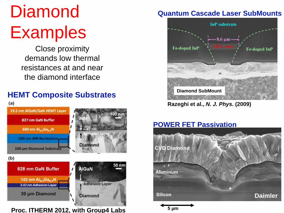
Razeghi et al., N. J. Phys. (2009)
Diamond SubMount HEMT Composite Substrates
POWER FET Passivation
Quantum Cascade Laser SubMounts
Daimler
Close proximity
demands low thermal
resistances at and near
the diamond interface
Diamond
Examples
Proc. ITHERM 2012, with Group4 Labs

Resistance Targets for GaN HEMTs
101
102
103
104
105
0
5
10
15
20
25
Heater width (nm)
Therm
al r
esi
stance
(K
/W/m
m)
Diamond
SiC
Bottom TBR
Solid (─) 0 m2K/GW
Dash (– –) 20 m2K/GW
Dot (▪▪▪▪) 50 m2K/GW
800nm GaN buffer layerK=150 W/m-K
HEMT Device
SiC or Diamond SubstrateK=390, or 1800 W/m-K
TBR
GaN-Diamond Boundary Resistance
0.1 1
better
m2K/GW 10 100
worse than SiC Diamond is ….… much
better

30 μm Diamond
828 nm GaN Buffer
3-42 nm Adhesion Layer
50 nm Al Transducer
142 nm AlGaN
• RGaN-Diamond = RAlGaN-ADH + RADH + RADH-Diamond
• kGaN and kAlGaN measured using independent sample sets
yielding 90 and 16.6 W/mK, respectively
24
Sam
ple
A
Measurement
Technique
RGaN-Diamond, A
[m2K/GW]
RGaN-Diamond, B
[m2K/GW]
Picosecond 22 ± 9 25 ± 13
DC Joule heating 25 ± 11 29 ± 12
Picosecond & DC Joule Heating
for GaN-on-Diamond Multilayers
30 μm Diamond
848 nm GaN Buffer
38-50 nm Adhesion Layer
50 nm Al Transducer
Sa
mp
le B
269 nm AlGaN
AlGaN
Diamond
Substrate
50 nm
10 µm
101
102
103
104
105
101
102
103
104
105
106
Heater width (nm)
Therm
al re
sis
tance (
K/W
)
Numerical solution
Experimental data
Patterned bridges,
50nm-5mm width
Stanford with Group4 Labs

Diamond & GaN in Composite Substrates
Boundary Resistance
0.1 1 m2K/GW 10 100
Kuball
2007, 2010
Raman
Kuzmik 2007
Interferometry,
Raman
GaN-diamond
target
Goodson 1995
10 ns TDTR
+ 20 m Bridge
Touzelbaev & Goodson 1998, 10 ns TDTR
GaN-SiC
GaN-diamond
Stanford
10 ps TDTR Northrop
Grumman Raytheon
TDTR
Uncertainty
better much better
Kuzmik 2011, Interferometry
Stanford, 10 ps TDTR + 50 nm Bridge
Group4
2010
Group4
2011
Diamond-Si
GaN-Si
Group4
+ 50 nm
Joule
heating
Diamond-ADH
Stanford
10 ps TDTR
Multithickness Group4

Outline
Metrology
GaN-Diamond HEMTs
Phase Change Memory
3D NanoPackaging
Microfluidic Cooling
http://www.nanoheat.stanford.edu

Pop, Sinha, Goodson, Proceedings IEEE (2006)
Rowlette, Goodson, IEEE Trans. Electron Devices (2008)
N(T)
300 K 343 K
Energy [meV]
1.0 V
@25 nm
960 K
Hot Phonons

Phase Change Memory

Phase Change Memory
Research Challenges • Multibit data storage (holy grail)
• Drift of reset resistance
& threshold voltage
• Interface transport
• Energy consumption (reset)
Tem
pera
ture
Cheng et al., IBM/Macronix, Proc IEDM 2011
Active
region
GeSbTe
Top Electrode
Bottom
Electrode

SiO2
PCMW W
Current (A)V GND
Thermal Characterization
Electrothermal/Crystallization Modeling
Jaeho Lee
Zijian Li
ThermoElectrics (Seebeck/Thomson)
Sample film (CNT Array)
Heat sink (silicon or metal substrate)
Metal coating
Nanosecond Heating from Nd:YAG
To
Detector
CW Radiation for
Thermometry
GST
Threshold & Reset Drift
Multibit Strategies and Novel Synthesis
PC
Amorphous Crystalline
Elah Bozorg-Grayeli
Zijian Li, Jeaho Lee
MicroThermal
Stage (MTS) Rakesh
Jeyasingh,
Jaeho Lee Jaeho Lee,
Rakesh Jeyasingh,
Zijian Li
Rakesh Jeyasingh
Zijian Li
Jaeho Lee
H.S.P Wong group (Stanford EE), Intel (Kau, Chang, Spandini), NXP (Hurckx),
Micron (Smythe), IBM (Raoux, Krebs)
National Science Foundation, Semiconductor Research Corporation
Sponsors &
Collaborators:
Phase Change Nanodevice Group
ThermoMechanics Yoonjin Won
Jaeho Lee

GST
TEC (W)
BEC (W)
HeaterSiO2
20 nm
50 nm
80 nm
20 nm
Φ40nm
80 nm80 nm
GST
TEC (W)
BEC (W)
SiO2
20 nm
50 nm
100 nm
20 nm
50 nm
Φ80nm
BEC (Bottom Electrode Contact)
MEC (Middle Electrode Contact)
TEC (Top Electrode Contact)
SiO2
R0 R1
R3 R2
GST
SiO2
GST
GST
Multibit
PCM
Design
Strategies
10 nm SiO2
40 nm GST
10 nm SiO2
100 nm GST
10 nm GST
TiNTiN
SiO2 / Si Substrate
80 nm 50 nm
Pulse-controlled MLC
• Standard manufacturing;
• Multiple programming
schemes available (tail
duration and pulse amplitude);
• Capable of more than 4
levels;
• Need write-and-verify;
• Subject to resistance drift.
Multilayer Stacked Design
Stacked Vertical Cell
• Four distinct resistance
levels;
• Low programming current;
• Precise control of
dimensions;
• Fabrication complexity;
Varying Width PC Structures
• Programming control with
variable width w3 > w2 > w1
• Susceptible to resistance drift
• Distinct levels of
resistance
•Thermally efficient
programming
• Fabrication
complexity
Electrode
Electrode
w3
w2
w1
w3 w2 w1
Lateral Configuration Vertical
PCRAM Multibit Design Geometries Wong, Goodson, Asheghi, et al., Proceedings of the IEEE (2011)

Future Phase Change Nanodevices
Field-Programmable
Gate Arrays
RF-FPGA
SyNAPSE
SL
m-1
SL
m+1SL
WL
n-1
WL
n+1
n
WL
n
Depressed Synapse
(amorphous state)
Potentiated Synapse
(crystalline state)
Pre spike line
Post spike line
GST
Bottom
electrode
Pre-synaptic neuron
Post-synaptic neuron
Neural signal
Synapse
Neural
signal
Dendrites
Nucleus
Axon hillock
Myelin sheath
Synapses for Brain-
Inspired Computing Kuzum, Jeyasingh, Lee, Wong,
Nano Letters (2011)
Lee, Asheghi, Wong, Goodson, et al.
Electron Device Letters (2011)

Outline
Metrology
GaN-Diamond HEMTs
Phase Change Memory
3D NanoPackaging
Microfluidic Cooling
http://www.nanoheat.stanford.edu

Logic
Memory Memory
Chip Carrier
IBM-3M Press Release
September 2011
3D Stacking Interfaces
3D NanoPackaging

Logic
Memory Memory
Chip Carrier
Primary Thermal
Interface 2011
Removable
backer
Nanofibers
Low melting temperature
binder (e.g. alloys of Ga, In, Sn)
Adhesion layer
Adhesion layer wets nanotubes and promotes
adhesion of binder (Pd, Pt, or Ti).
~100 nm is the
typical variation in
CNT height.
Hu, Fisher, Goodson, et al., J. Heat Transfer (2006)
SRC Patent: Hu, Jiang, Goodson, US Patent 7,504,453, issued 2009
SRC Patent: Panzer, Goodson, et al., 2009/0068387 (pending)
3D NanoPackaging

Logic
Memory Memory
Chip Carrier
Carbon 2012
Primary Thermal
Interface
2010
3D NanoPackaging

Logic
Memory Memory
Chip Carrier
3D Stacking Interfaces
2011
Axia
lTransverse
CNT
Composites
3D NanoPackaging
Sample Complexity
Rig
Co
mp
lexit
y
SAMPLE FILM
Kaeding, Skurk, Goodson,
Applied Physics Letters (1993)
Pump-probe optics
Hybrid Optical-Electrical Methods
Multi-property Measurements
Nano Thermal Metrology

Mechanical & Thermal Properties of
Aligned CNT Films
750 µm
50 µm
Thermal Mechanical
Pump Laser Doppler Vibrometer (LDV)
Piezoelectric Shaker
Probe
Si substrate
Polysilicon Oxide Al2O3
Fe CNT
Yoonjin Won, Matt Panzer, Amy Marconnet
Carbon (2012). SRC 1640 (ended), 1966
MEMS Resonator

GOAL
Thermal Interface Materials (TIM)
Properties
Thermal Resistivity (m K / W) 1.0 0.1
Ela
sti
c M
od
ulu
s (
MP
a)
Greases
& Gels
Phase
Change
Materials
Indium/
Solders Adhesives
0.01
Nano-
gels
Lifetime
thermal cycling
104
103
102
101
Latest
Stanford CNT
Data1
1 Gao, Goodson, et al., J. Electronic Materials (2010).
Won, Goodson, et al., Carbon (2011) 40
Long-
Anticipated
Publication in
CARBON
(2011)
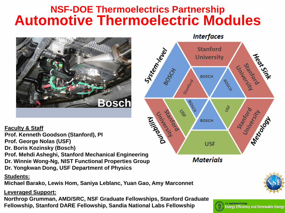
NSF-DOE Thermoelectrics Partnership
Automotive Thermoelectric Modules
Faculty & Staff
Prof. Kenneth Goodson (Stanford), PI
Prof. George Nolas (USF)
Dr. Boris Kozinsky (Bosch)
Prof. Mehdi Asheghi, Stanford Mechanical Engineering
Dr. Winnie Wong-Ng, NIST Functional Properties Group
Dr. Yongkwan Dong, USF Department of Physics
Students:
Michael Barako, Lewis Hom, Saniya Leblanc, Yuan Gao, Amy Marconnet
Leveraged Support:
Northrop Grumman, AMD/SRC, NSF Graduate Fellowships, Stanford Graduate
Fellowship, Stanford DARE Fellowship, Sandia National Labs Fellowship
Bosch
Outline
Metrology
GaN-Diamond HEMTs
Phase Change Memory
3D NanoPackaging
Microfluidic Cooling
http://www.nanoheat.stanford.edu

Microfluidics Cooling Trajectory
1985 1990 2000 2010 2005
IBM Thermal
conduction module
Tuckerman & Pease
microchannel
demonstration
Microchannel
implementation in
laser diode cooling
Extensive single/two-
phase flow research DARPA
Programs
Toshiba &
Hitachi
Laptops
Apple G5
Liquid Cooling goes primetime
100
W/Cm2
300+
W/Cm2
3D
microfluidics
Two-phase
flow
Fluid Design
Nano
Surfaces
Multicore

Instrumented Microfluidic Platform
400 m
Back Side Front Side
Doped Si Sensor
Al Heater
100 m
Kramer, Flynn, Fogg, Wang, Hidrovo, Prasher, Chau, Narasimhan, Goodson. “Microchannel
Experimental Structure for Measuring Temperature Fields During Convective Boiling,” ASME
International Mechanical Engineering Congress & Exposition, Anaheim, CA, USA, November 13-19,
2004, IMECE2004-61936.

IEEE Transactions on Components and Packaging Technology (2002)
2000 2002 2004
DARPA funding
Intel
Apple
AMD
Research Background
Cooligy
Startup
(VC funding)
MicroCoolers for Computers
Acquisition
By Emerson
2006 2008
~600W total
~ 1kW/cm2
Best Paper at SEMITHERM 2001
Product Win
100K+ Units
Trajectory of a Startup (Cooligy)

2000 2002 2004
DARPA funding
Intel
Apple
AMD
Research Background
Trajectory of a Startup (Cooligy) Micro hx
EO Pump
Heatrejector
Micro hx
EO Pump
Heatrejector
Zhou et al., Proc. SEMITHERM 2004, Proc. ITHERM 2004
Si chip
Fluid
inlet Outlet Thermal
attach 3D
Cooligy
Startup
(VC funding)
Product Win
100K+ Units
MicroCoolers for Computers
Acquisition
By Emerson
2006 2008
~600W total
~ 1kW/cm2
Liquid
Cooling
Challenge

Vapor Escape
Microfluidic HX
Prototype
Vapor-transmitting membrane
reduces pressure drop and
instabilities along two-phase
micro HX.
Latest data show 60% pressure
drop and nearly 50% drop in
excess temperature over inlet
saturation.
2 ml/min, G = 103 kg/s/m2
0
5
10
15
20
25
0 10 20 30 40 50 60 70
Eff. Heat Flux [W/cm2]
DP
tot /
DP
lo
Control
Vent
SIM Control
SIM Vent
Liquid IN
Liquid + Vapor
OUT
Heat Flux from
AMD Test Chip
Vapor
OUT
Vapor
OUT
60-100 um thick, 50-220 nm pore,
hydrophobic porous PTFE
125 um square
plastic/copper
vapor channels
125 um square
copper liquid
channels with
12 embedded
thermocouples
International Journal of Heat and Mass
Transfer (2011)
International Journal of Multiphase Flow
(2011)
Students: Milnes David, Roger Flynn,
Julie Steinbrenner, Chen Fang, Joe Miler
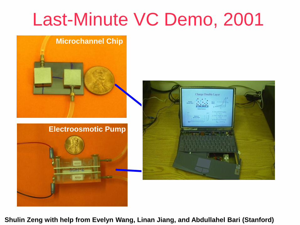
Last-Minute VC Demo, 2001 Microchannel Chip
Electroosmotic Pump
Heat Rejecter Coil & Plate
Sony VAIO Laptop Demo
Shulin Zeng with help from Evelyn Wang, Linan Jiang, and Abdullahel Bari (Stanford)

Selected Alumni
Prof. Dan Fletcher UC Berkeley Dr. Jeremy Rowlette Daylight Solns
Prof. Evelyn Wang MIT Dr. Patricia Gharagozloo Sandia Labs
Prof. Katsuo Kurabayashi U. Michigan Dr. Per Sverdrup Intel
Prof. Sungtaek Ju UCLA Dr. Chen Fang Exxon-Mobile
Prof. Mehdi Asheghi Stanford Dr. Milnes David IBM
Prof. Bill King UIUC Dr. Max Touzelbaev AMD
Prof. Eric Pop UIUC (EE) Dr. Roger Flynn Intel
Prof. Sanjiv Sinha UIUC Dr. Julie Steinbrenner Xerox Parc
Prof. Xeujiao Hu Wuhan Univ. Dr. John Reifenberg Intel
Prof. Carlos Hidrovo UT Austin Dr. David Fogg Creare
Prof. Kaustav Banerjee UCSB (EE) Dr. Matthew Panzer KLA-Tencor
Prof. Ankur Jain UT Arlington
Prof. Sarah Parikh Foothill College
Current Group Ken Goodson
Josef Miler Elah Bozorg-Grayeli Lewis Hom
Michael Barako Amy Marconnet Aditja Sood (MSE)
Jaeho Lee Shilpi Roy (EE) Woosung Parc
Sri Lingamneni Yuan Gao
Saniya Leblanc Yiyang Li (MSE) Dr. Takashi Kodama
Jungwan Cho Zijian Li Dr. Yoonjin Won
Prof. Mehdi Asheghi
Recommended