Patterning of colloidal quantum dots forthe generation of surface plasmon
Yeonsang ParkYoung-Geun RohUn Jeong KimDae-Young ChungHwansoo SuhJineun KimSangmo CheonJaesoong LeeTae-Ho KimKyung-Sang ChoChang-Won Lee
Patterning of colloidal quantum dots for the generationof surface plasmon
Yeonsang ParkYoung-Geun RohUn Jeong KimDae-Young ChungHwansoo SuhJineun KimSangmo CheonJaesoong LeeTae-Ho KimKyung-Sang ChoChang-Won LeeSamsung Advanced Institute of TechnologyFrontier Research LabYongin-si, Kyonggi-do 446-712, Republic of KoreaE-mail: [email protected]
Abstract. Patterning of colloidal quantum dot (QD) of a nanometer res-olution is important for potential applications in micro- or nanophotonics.Several patterning techniques such as polymer composites, molecularkey-lock methods, inkjet printing, and the microcontact printing of QDshave been successfully developed and applied to various plasmonicapplications. However, these methods are not easily adapted to conven-tional complementary metal-oxide semiconductor (CMOS)-compatibleprocesses because of either limits in fabrication resolutions or difficultiesin sub-100-nm alignment. Here, we present an adaptation of a conven-tional lift-off method for the patterning of colloidal QDs. This simple methodcan be later applied to CMOS processes by changing electron beamlithography to photolithography for building up photon-generation ele-ments in various planar geometries. Various shapes formed by colloidalQD clusters such as straight lines, rings, and dot patterns with sub-100-nmsize could be fabricated. The patterned structures show sub-10-nm posi-tioning with good fluorescence properties and well-defined sidewallprofiles. To demonstrate the applicability of our method, we present a sur-face plasmon generator from a QD cluster. © 2013 Society of Photo-OpticalInstrumentation Engineers (SPIE) [DOI: 10.1117/1.JMM.12.4.041202]
Subject terms: colloidal quantum dot; nanoscale patterning; electron beam lithog-raphy; lift-off process; surface plasmon generator; finite-difference time-domainsimulation.
Paper 13022SSP received Mar. 11, 2013; revised manuscript received Apr. 26,2013; accepted for publication May 7, 2013; published online Sep. 25, 2013.
1 IntroductionSince its invention, the colloidal quantum dot (QD) hasattracted interest due to its broad functionalities and applica-bilities.1,2 Owing to the quantum confinement effect, theoptical spectrum of QDs moves to a higher energy levelupon a decrease in the size of the material.3–6 In addition,high internal radiative efficiency holds promise for variousphotonic7–10 and plasmonic applications.11–13 In spite ofthe numerous advantages of QDs, the microfabrication ofcolloidal QDs into one-dimensional (1-D) or two-dimen-sional (2-D) structures is still quite challenging because ofsolubility issues and the wetting properties on oxide and met-allic substrates. These difficulties result in restricted usageand applications of QDs in diverse fields of photonics andplasmonics. To overcome these constraints, researchershave successfully developed methods of patterning mixturesof a photosensitive polymer and QDs.14–17 The photo-curingpatterning of nanocrystals shows fabrication resolutionslarger than 2 μm and reduced luminescence intensity perunit volume compared to that of pristine QDs. The micro-contact printing method has shown unique advantagessuch as ease of use and high throughput with a sub-microm-eter-scale resolution.18–20 However, it has difficulty in align-ment between the mold and the predefined nanostructure andbecomes disadvantageous in situations where only a fractionof the size of the mold has to be stamped. Recently, a fewresearch groups devised method of patterning QDs with aself-assembled monolayer (SAM) treatment, called molecule
key-lock method.21–24 This method uses a SAM chemicaltreatment of a region to be patterned followed by a QD coat-ing of the surface. Once a key-lock pair is formed betweenthe patterned SAM molecule and the ligand molecule of theQDs, excessive QDs can be easily removed from the surface,leaving only the patterned QDs on top of the predefinedSAM of key molecules. However, this method requires addi-tional chemical combinations of the key-lock pair moleculesfor more than two types of QDs.
In this letter, we present a simple patterning process forcolloidal QDs similar to a conventional lift-off process. Thisapproach facilitates fabrication processes for defining high-resolution 1-D and 2-D structures without a complicated sur-face treatment process and/or a delicate choice of a key-lockmolecule pair. With our approach, arbitrary shapes com-posed of QDs can be patterned onto a designated location.This method, unlike the microcontact printing method, canbe applied even for defining sparse patterns. Our methodopens up the possibility of acquiring complementary metal-oxide semiconductor (CMOS) compatibility with colloidalQDs as local photonic and plasmonic sources on a planarmetal or oxide surface. We successfully fabricated 1-Dstraight-line and 2-D ring structures made of colloidal QDswith linewidths of a few hundreds of nanometers. As anextreme case of patterning, we fabricated zero-dimensional(0-D) dot with a few tens of a nanometer diameter. TheQD nanostructures fabricated on a metallic plane could beused for surface plasmons (SP) launchers where fabricationresolution on the sub-100-nm scale plays a significant role.0091-3286/2013/$25.00 © 2013 SPIE
J. Micro/Nanolith. MEMS MOEMS 041202-1 Oct–Dec 2013/Vol. 12(4)
J. Micro/Nanolith. MEMS MOEMS 12(4), 041202 (Oct–Dec 2013)
2 Experiment
2.1 Sample Preparation
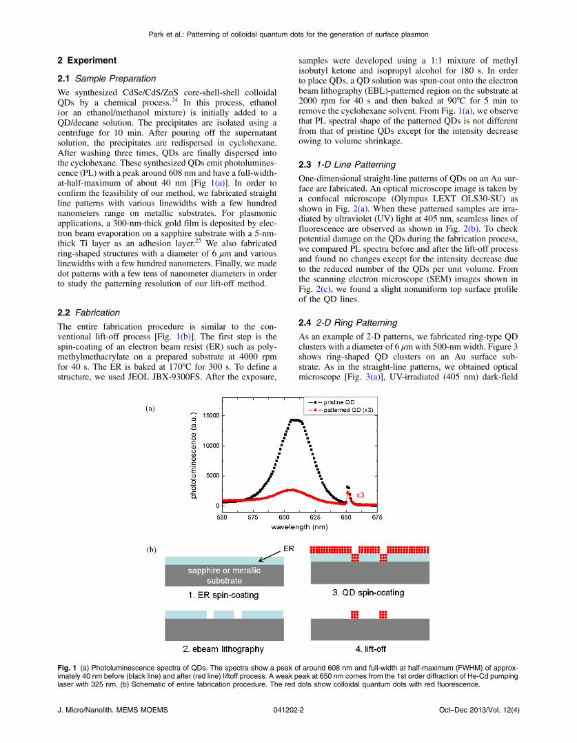
We synthesized CdSe/CdS/ZnS core-shell-shell colloidalQDs by a chemical process.24 In this process, ethanol(or an ethanol/methanol mixture) is initially added to aQD/decane solution. The precipitates are isolated using acentrifuge for 10 min. After pouring off the supernatantsolution, the precipitates are redispersed in cyclohexane.After washing three times, QDs are finally dispersed intothe cyclohexane. These synthesized QDs emit photolumines-cence (PL) with a peak around 608 nm and have a full-width-at-half-maximum of about 40 nm [Fig 1(a)]. In order toconfirm the feasibility of our method, we fabricated straightline patterns with various linewidths with a few hundrednanometers range on metallic substrates. For plasmonicapplications, a 300-nm-thick gold film is deposited by elec-tron beam evaporation on a sapphire substrate with a 5-nm-thick Ti layer as an adhesion layer.25 We also fabricatedring-shaped structures with a diameter of 6 μm and variouslinewidths with a few hundred nanometers. Finally, we madedot patterns with a few tens of nanometer diameters in orderto study the patterning resolution of our lift-off method.
2.2 Fabrication
The entire fabrication procedure is similar to the con-ventional lift-off process [Fig. 1(b)]. The first step is thespin-coating of an electron beam resist (ER) such as poly-methylmethacrylate on a prepared substrate at 4000 rpmfor 40 s. The ER is baked at 170°C for 300 s. To define astructure, we used JEOL JBX-9300FS. After the exposure,
samples were developed using a 1:1 mixture of methylisobutyl ketone and isopropyl alcohol for 180 s. In orderto place QDs, a QD solution was spun-coat onto the electronbeam lithography (EBL)-patterned region on the substrate at2000 rpm for 40 s and then baked at 90°C for 5 min toremove the cyclohexane solvent. From Fig. 1(a), we observethat PL spectral shape of the patterned QDs is not differentfrom that of pristine QDs except for the intensity decreaseowing to volume shrinkage.
2.3 1-D Line Patterning
One-dimensional straight-line patterns of QDs on an Au sur-face are fabricated. An optical microscope image is taken bya confocal microscope (Olympus LEXT OLS30-SU) asshown in Fig. 2(a). When these patterned samples are irra-diated by ultraviolet (UV) light at 405 nm, seamless lines offluorescence are observed as shown in Fig. 2(b). To checkpotential damage on the QDs during the fabrication process,we compared PL spectra before and after the lift-off processand found no changes except for the intensity decrease dueto the reduced number of the QDs per unit volume. Fromthe scanning electron microscope (SEM) images shown inFig. 2(c), we found a slight nonuniform top surface profileof the QD lines.
2.4 2-D Ring Patterning
As an example of 2-D patterns, we fabricated ring-type QDclusters with a diameter of 6 μmwith 500-nm width. Figure 3shows ring-shaped QD clusters on an Au surface sub-strate. As in the straight-line patterns, we obtained opticalmicroscope [Fig. 3(a)], UV-irradiated (405 nm) dark-field
Fig. 1 (a) Photoluminescence spectra of QDs. The spectra show a peak of around 608 nm and full-width at half-maximum (FWHM) of approx-imately 40 nm before (black line) and after (red line) liftoff process. A weak peak at 650 nm comes from the 1st order diffraction of He-Cd pumpinglaser with 325 nm. (b) Schematic of entire fabrication procedure. The red dots show colloidal quantum dots with red fluorescence.
J. Micro/Nanolith. MEMS MOEMS 041202-2 Oct–Dec 2013/Vol. 12(4)
Park et al.: Patterning of colloidal quantum dots for the generation of surface plasmon
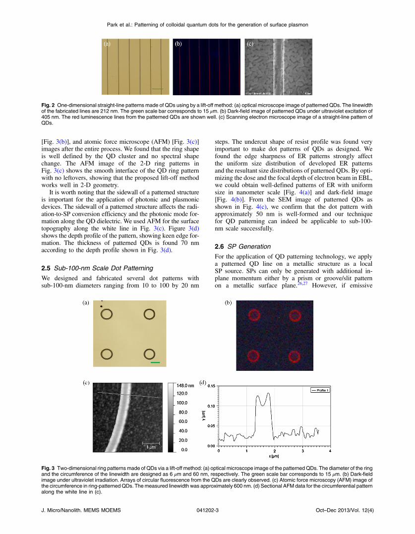
[Fig. 3(b)], and atomic force microscope (AFM) [Fig. 3(c)]images after the entire process. We found that the ring shapeis well defined by the QD cluster and no spectral shapechange. The AFM image of the 2-D ring patterns inFig. 3(c) shows the smooth interface of the QD ring patternwith no leftovers, showing that the proposed lift-off methodworks well in 2-D geometry.
It is worth noting that the sidewall of a patterned structureis important for the application of photonic and plasmonicdevices. The sidewall of a patterned structure affects the radi-ation-to-SP conversion efficiency and the photonic mode for-mation along the QD dielectric. We used AFM for the surfacetopography along the white line in Fig. 3(c). Figure 3(d)shows the depth profile of the pattern, showing keen edge for-mation. The thickness of patterned QDs is found 70 nmaccording to the depth profile shown in Fig. 3(d).
2.5 Sub-100-nm Scale Dot Patterning
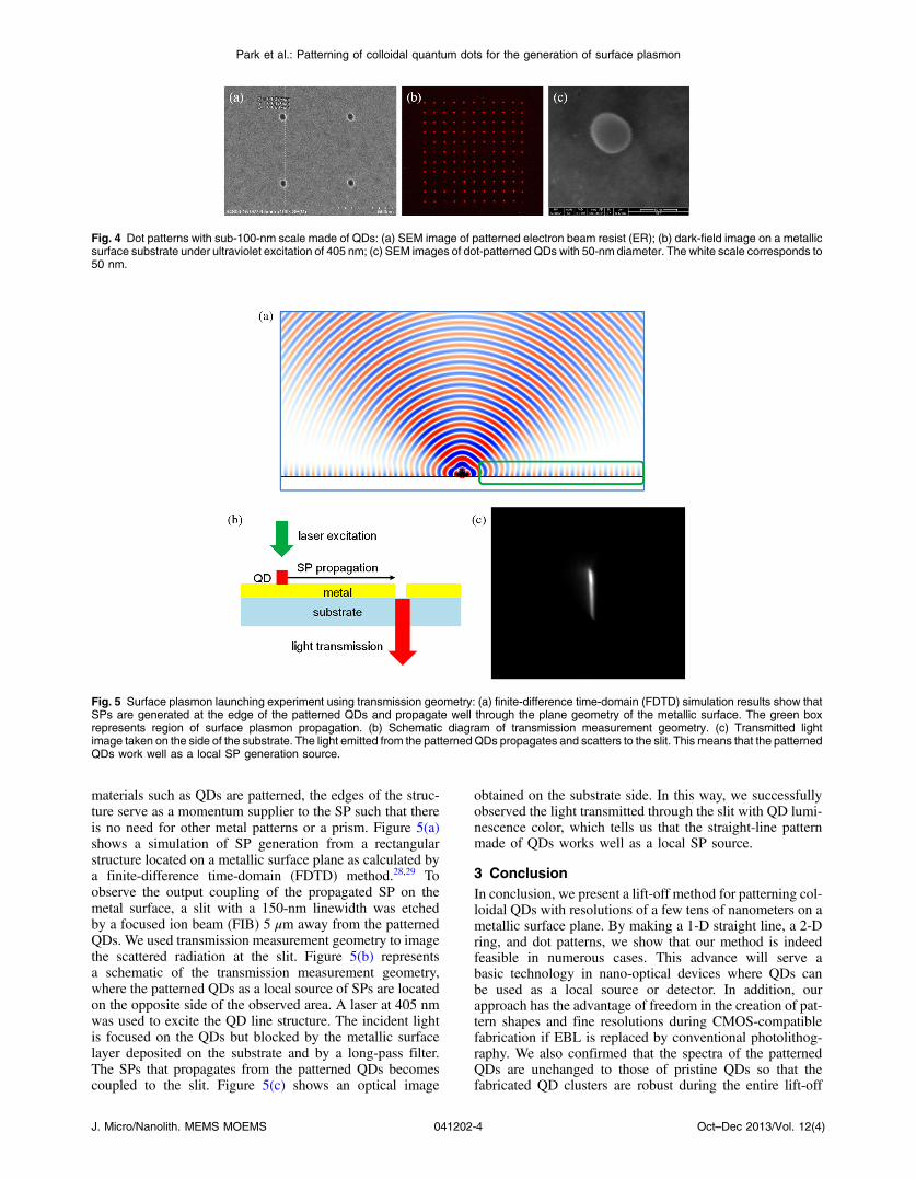
We designed and fabricated several dot patterns withsub-100-nm diameters ranging from 10 to 100 by 20 nm
steps. The undercut shape of resist profile was found veryimportant to make dot patterns of QDs as designed. Wefound the edge sharpness of ER patterns strongly affectthe uniform size distribution of developed ER patternsand the resultant size distributions of patterned QDs. By opti-mizing the dose and the focal depth of electron beam in EBL,we could obtain well-defined patterns of ER with uniformsize in nanometer scale [Fig. 4(a)] and dark-field image[Fig. 4(b)]. From the SEM image of patterned QDs asshown in Fig. 4(c), we confirm that the dot pattern withapproximately 50 nm is well-formed and our techniquefor QD patterning can indeed be applicable to sub-100-nm scale successfully.
2.6 SP Generation
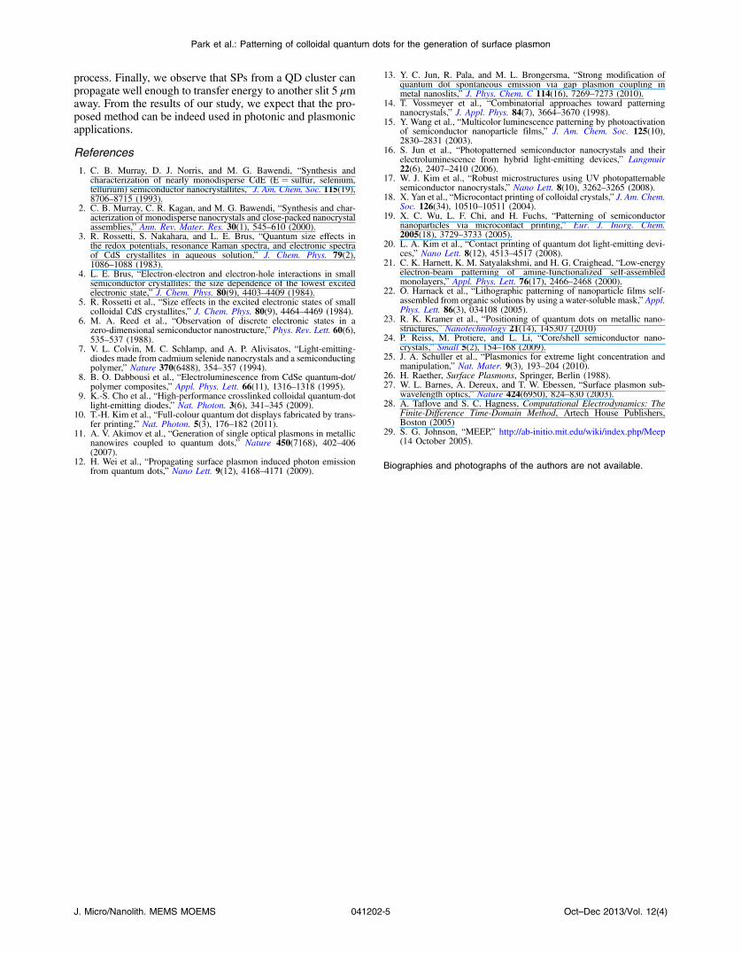
For the application of QD patterning technology, we applya patterned QD line on a metallic structure as a localSP source. SPs can only be generated with additional in-plane momentum either by a prism or groove/slit patternon a metallic surface plane.26,27 However, if emissive
Fig. 2 One-dimensional straight-line patterns made of QDs using by a lift-off method: (a) optical microscope image of patterned QDs. The linewidthof the fabricated lines are 212 nm. The green scale bar corresponds to 15 μm. (b) Dark-field image of patterned QDs under ultraviolet excitation of405 nm. The red luminescence lines from the patterned QDs are shown well. (c) Scanning electron microscope image of a straight-line pattern ofQDs.
Fig. 3 Two-dimensional ring patterns made of QDs via a lift-off method: (a) optical microscope image of the patterned QDs. The diameter of the ringand the circumference of the linewidth are designed as 6 μm and 60 nm, respectively. The green scale bar corresponds to 15 μm. (b) Dark-fieldimage under ultraviolet irradiation. Arrays of circular fluorescence from the QDs are clearly observed. (c) Atomic force microscopy (AFM) image ofthe circumference in ring-patterned QDs. Themeasured linewidth was approximately 600 nm. (d) Sectional AFM data for the circumferential patternalong the white line in (c).
J. Micro/Nanolith. MEMS MOEMS 041202-3 Oct–Dec 2013/Vol. 12(4)
Park et al.: Patterning of colloidal quantum dots for the generation of surface plasmon
materials such as QDs are patterned, the edges of the struc-ture serve as a momentum supplier to the SP such that thereis no need for other metal patterns or a prism. Figure 5(a)shows a simulation of SP generation from a rectangularstructure located on a metallic surface plane as calculated bya finite-difference time-domain (FDTD) method.28,29 Toobserve the output coupling of the propagated SP on themetal surface, a slit with a 150-nm linewidth was etchedby a focused ion beam (FIB) 5 μm away from the patternedQDs. We used transmission measurement geometry to imagethe scattered radiation at the slit. Figure 5(b) representsa schematic of the transmission measurement geometry,where the patterned QDs as a local source of SPs are locatedon the opposite side of the observed area. A laser at 405 nmwas used to excite the QD line structure. The incident lightis focused on the QDs but blocked by the metallic surfacelayer deposited on the substrate and by a long-pass filter.The SPs that propagates from the patterned QDs becomescoupled to the slit. Figure 5(c) shows an optical image
obtained on the substrate side. In this way, we successfullyobserved the light transmitted through the slit with QD lumi-nescence color, which tells us that the straight-line patternmade of QDs works well as a local SP source.
3 ConclusionIn conclusion, we present a lift-off method for patterning col-loidal QDs with resolutions of a few tens of nanometers on ametallic surface plane. By making a 1-D straight line, a 2-Dring, and dot patterns, we show that our method is indeedfeasible in numerous cases. This advance will serve abasic technology in nano-optical devices where QDs canbe used as a local source or detector. In addition, ourapproach has the advantage of freedom in the creation of pat-tern shapes and fine resolutions during CMOS-compatiblefabrication if EBL is replaced by conventional photolithog-raphy. We also confirmed that the spectra of the patternedQDs are unchanged to those of pristine QDs so that thefabricated QD clusters are robust during the entire lift-off
Fig. 4 Dot patterns with sub-100-nm scale made of QDs: (a) SEM image of patterned electron beam resist (ER); (b) dark-field image on a metallicsurface substrate under ultraviolet excitation of 405 nm; (c) SEM images of dot-patterned QDs with 50-nm diameter. The white scale corresponds to50 nm.
Fig. 5 Surface plasmon launching experiment using transmission geometry: (a) finite-difference time-domain (FDTD) simulation results show thatSPs are generated at the edge of the patterned QDs and propagate well through the plane geometry of the metallic surface. The green boxrepresents region of surface plasmon propagation. (b) Schematic diagram of transmission measurement geometry. (c) Transmitted lightimage taken on the side of the substrate. The light emitted from the patternedQDs propagates and scatters to the slit. This means that the patternedQDs work well as a local SP generation source.
J. Micro/Nanolith. MEMS MOEMS 041202-4 Oct–Dec 2013/Vol. 12(4)
Park et al.: Patterning of colloidal quantum dots for the generation of surface plasmon
process. Finally, we observe that SPs from a QD cluster canpropagate well enough to transfer energy to another slit 5 μmaway. From the results of our study, we expect that the pro-posed method can be indeed used in photonic and plasmonicapplications.
References
1. C. B. Murray, D. J. Norris, and M. G. Bawendi, “Synthesis andcharacterization of nearly monodisperse CdE (E ¼ sulfur, selenium,tellurium) semiconductor nanocrystallites,” J. Am. Chem. Soc. 115(19),8706–8715 (1993).
2. C. B. Murray, C. R. Kagan, and M. G. Bawendi, “Synthesis and char-acterization of monodisperse nanocrystals and close-packed nanocrystalassemblies,” Ann. Rev. Mater. Res. 30(1), 545–610 (2000).
3. R. Rossetti, S. Nakahara, and L. E. Brus, “Quantum size effects inthe redox potentials, resonance Raman spectra, and electronic spectraof CdS crystallites in aqueous solution,” J. Chem. Phys. 79(2),1086–1088 (1983).
4. L. E. Brus, “Electron-electron and electron-hole interactions in smallsemiconductor crystallites: the size dependence of the lowest excitedelectronic state,” J. Chem. Phys. 80(9), 4403–4409 (1984).
5. R. Rossetti et al., “Size effects in the excited electronic states of smallcolloidal CdS crystallites,” J. Chem. Phys. 80(9), 4464–4469 (1984).
6. M. A. Reed et al., “Observation of discrete electronic states in azero-dimensional semiconductor nanostructure,” Phys. Rev. Lett. 60(6),535–537 (1988).
7. V. L. Colvin, M. C. Schlamp, and A. P. Alivisatos, “Light-emitting-diodes made from cadmium selenide nanocrystals and a semiconductingpolymer,” Nature 370(6488), 354–357 (1994).
8. B. O. Dabbousi et al., “Electroluminescence from CdSe quantum‐dot/polymer composites,” Appl. Phys. Lett. 66(11), 1316–1318 (1995).
9. K.-S. Cho et al., “High-performance crosslinked colloidal quantum-dotlight-emitting diodes,” Nat. Photon. 3(6), 341–345 (2009).
10. T.-H. Kim et al., “Full-colour quantum dot displays fabricated by trans-fer printing,” Nat. Photon. 5(3), 176–182 (2011).
11. A. V. Akimov et al., “Generation of single optical plasmons in metallicnanowires coupled to quantum dots,” Nature 450(7168), 402–406(2007).
12. H. Wei et al., “Propagating surface plasmon induced photon emissionfrom quantum dots,” Nano Lett. 9(12), 4168–4171 (2009).
13. Y. C. Jun, R. Pala, and M. L. Brongersma, “Strong modification ofquantum dot spontaneous emission via gap plasmon coupling inmetal nanoslits,” J. Phys. Chem. C 114(16), 7269–7273 (2010).
14. T. Vossmeyer et al., “Combinatorial approaches toward patterningnanocrystals,” J. Appl. Phys. 84(7), 3664–3670 (1998).
15. Y. Wang et al., “Multicolor luminescence patterning by photoactivationof semiconductor nanoparticle films,” J. Am. Chem. Soc. 125(10),2830–2831 (2003).
16. S. Jun et al., “Photopatterned semiconductor nanocrystals and theirelectroluminescence from hybrid light-emitting devices,” Langmuir22(6), 2407–2410 (2006).
17. W. J. Kim et al., “Robust microstructures using UV photopatternablesemiconductor nanocrystals,” Nano Lett. 8(10), 3262–3265 (2008).
18. X. Yan et al., “Microcontact printing of colloidal crystals,” J. Am. Chem.Soc. 126(34), 10510–10511 (2004).
19. X. C. Wu, L. F. Chi, and H. Fuchs, “Patterning of semiconductornanoparticles via microcontact printing,” Eur. J. Inorg. Chem.2005(18), 3729–3733 (2005).
20. L. A. Kim et al., “Contact printing of quantum dot light-emitting devi-ces,” Nano Lett. 8(12), 4513–4517 (2008).
21. C. K. Harnett, K. M. Satyalakshmi, and H. G. Craighead, “Low-energyelectron-beam patterning of amine-functionalized self-assembledmonolayers,” Appl. Phys. Lett. 76(17), 2466–2468 (2000).
22. O. Harnack et al., “Lithographic patterning of nanoparticle films self-assembled from organic solutions by using a water-soluble mask,” Appl.Phys. Lett. 86(3), 034108 (2005).
23. R. K. Kramer et al., “Positioning of quantum dots on metallic nano-structures,” Nanotechnology 21(14), 145307 (2010)
24. P. Reiss, M. Protiere, and L. Li, “Core/shell semiconductor nano-crystals,” Small 5(2), 154–168 (2009).
25. J. A. Schuller et al., “Plasmonics for extreme light concentration andmanipulation,” Nat. Mater. 9(3), 193–204 (2010).
26. H. Raether, Surface Plasmons, Springer, Berlin (1988).27. W. L. Barnes, A. Dereux, and T. W. Ebessen, “Surface plasmon sub-
wavelength optics,” Nature 424(6950), 824–830 (2003).28. A. Taflove and S. C. Hagness, Computational Electrodynamics: The
Finite-Difference Time-Domain Method, Artech House Publishers,Boston (2005)
29. S. G. Johnson, “MEEP,” http://ab-initio.mit.edu/wiki/index.php/Meep(14 October 2005).
Biographies and photographs of the authors are not available.
J. Micro/Nanolith. MEMS MOEMS 041202-5 Oct–Dec 2013/Vol. 12(4)
Park et al.: Patterning of colloidal quantum dots for the generation of surface plasmon
Recommended