Embed Size (px)
Citation preview
IEEE JOURNAL OF SOLID-STATE CIRCUITS, VOL. 42, NO. 12, DECEMBER 2007 2715
40-Gb/s High-Gain Distributed Amplifiers WithCascaded Gain Stages in 0.18-�m CMOS
Jun-Chau Chien, Student Member, IEEE, and Liang-Hung Lu, Member, IEEE
Abstract—A novel circuit topology for high-gain distributed am-plifiers is presented in this study. Based on the conventional dis-tributed architecture, the gain cells are realized by cascading cas-code stages for gain enhancement. In addition, the stagger-tuningtechnique is extensively utilized in the design of the cascode stagesas well as the cascaded stages, leading to significant improvementin terms of the operating bandwidth and the gain flatness. With theproposed circuit architecture, two amplifiers are implemented in astandard 0.18- m CMOS technology. The amplifier with a 3 3configuration exhibits a gain of 16.2 dB and a 3-dB bandwidth of33.4 GHz, while the one in a form of 2 4 demonstrates a gainof 20 dB and a bandwidth of 39.4 GHz. Consuming a dc powerof 260 mW from a 2.8-V supply voltage, both circuits provide cleareye-opening with a pseudorandom bit sequence (PRBS) at 40 Gb/s.
Index Terms—Bandwidth enhancement, distributed amplifiers,gain–bandwidth product, gain flatness, inductive peaking, stagger-tuning technique.
I. INTRODUCTION
DUE TO THE increasing demand in the capacity of datacommunications, implementation of systems operating at
a data rate beyond 10 Gb/s has attracted great attention in thepast decade. With the advances in semiconductor technologies,integrated circuits operating at 40 Gb/s have been realized instandard CMOS processes [1]–[5]. Among all kinds of high-speed circuits, the broadband amplifier is a key building blockat both the transmitting and the receiving ends. Recently, sev-eral CMOS broadband amplifiers with bandwidth-enhancementtechniques have been reported [6]–[10].
In conventional circuit implementations, the gain-bandwidthproduct of broadband amplifiers is severely limited by theprocess technology. For high-speed operations, the amplifiergain is often sacrificed for an adequate bandwidth. Therefore,most of the 40-Gb/s amplifiers suffer from a limited gain [9],[10]. In order to overcome the design limitations, a novel circuitarchitecture for broadband amplifiers is proposed in this study[11]. By replacing the gain cells in the conventional distributedamplifiers (DAs) with cascaded stages, the gain is effectivelyenhanced. In addition, due to the use of inductive peaking withthe stagger-tuning technique, a remarkable 3-dB bandwidth canbe achieved while maintaining excellent gain flatness withinthe entire frequency band.
Manuscript received April 11, 2007; revised August 27, 2007. This work wassupported in part by the National Science Council under Grants 96-2220-E-002-016 and 96-2220-E-002-018.
The authors are with the Department of Electrical Engineering and GraduateInstitute of Electronics Engineering, National Taiwan University, Taipei 10617,Taiwan, R.O.C. (e-mail: [email protected]).
Digital Object Identifier 10.1109/JSSC.2007.908688
Fig. 1. Simplified circuit schematic of a 1-D DA.
This paper is organized as follows. Section II discusses theexisting architectures for broadband amplifiers and introducesthe proposed circuit configuration. Detailed circuit design andexperimental results of the 40-Gb/s high-gain DAs are presentedin Sections III and IV, respectively. Finally, conclusions are pro-vided in Section V.
II. AMPLIFIER ARCHITECTURE
A. Conventional DA
Distributed circuit techniques are widely used for the broad-band amplifiers in high-speed data links [10]–[16] as well asthe low-noise amplifiers in ultra-wideband (UWB) systems[17]–[19]. Fig. 1 shows the simplified schematic of the conven-tional one-dimensional (1-D) DA. Note that each gain cell isrepresented by a common-source stage for simplicity. By prop-erly choosing the transistor sizes and the inductance values, theinput and the output of the amplifier can be treated as 50-artificial transmission lines, demonstrating extremely widebandfrequency response with low input and output return losses. Inorder to maximize the gain of the amplifier, the phase delaysof the input and the output transmission lines are typicallymatched. Therefore, the currents generated by the individualgain cells can be added constructively at the output of theamplifier. Assuming that the transmission lines are lossless, thelow-frequency gain of the 1-D DA can be estimated by
(1)
where is the number of the distributed stages, representsthe transconductance of each stage, and is the terminationimpedance for the output transmission line, which is typically50 . Note that the coefficient 1/2 in (1) indicates that half of thesignal current propagates in an opposite direction towards thedrain termination. The characteristic impedance and the phasevelocity of the artificial transmission lines can be expressed as
(2)
(3)
0018-9200/$25.00 © 2007 IEEE
2716 IEEE JOURNAL OF SOLID-STATE CIRCUITS, VOL. 42, NO. 12, DECEMBER 2007
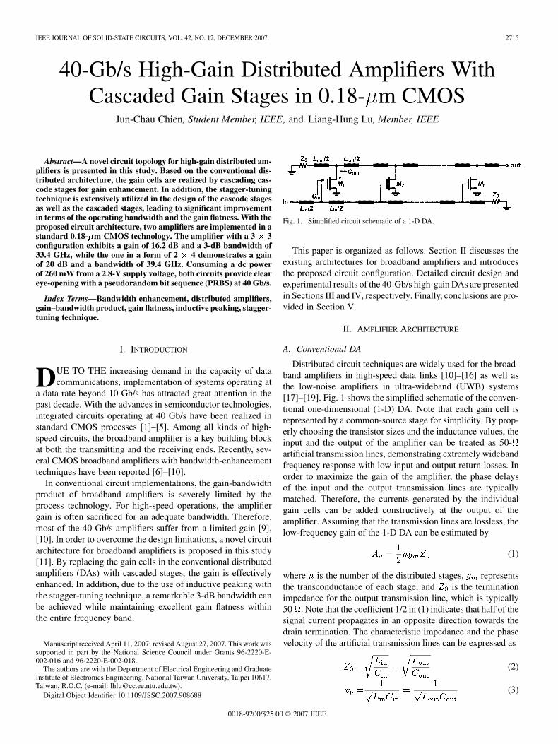
Fig. 2. Small-signal equivalent circuits for a single DA section at (a) the inputline and (b) the output line.
respectively. It is noted that the bandwidth of the DA is primarilydetermined by the cutoff frequencies of the artificial trans-mission lines, which are given by
(4)
Theoretically, the gain of the 1-D DA can be increased byadding more distributed cells. However, the series losses fromthe on-chip inductors as well as the input gate resistance andthe finite output resistance of the transistors severely limit themaximum number of cells. Fig. 2 shows the equivalent small-signal models of a single DA section at the gate and the drainlines. By applying series-to-parallel impedance transformation,the propagation constant for both artificial transmission linescan be expressed as [20]
(5)
(6)
where
(7)
(8)
Based on the circuit models, and are the inductive ele-ments of the transmission lines, while and are the seriesresistances associated with the respective inductors. The deviceparameters of the gain cells are represented by , , ,and . From (5) and (6), the expressions of the attenuationconstants for the gate and the drain line can be simplified as [20]
(9)
(10)
where and are the physical lengths of a unit section. It isnoted that, along the transmission line, the attenuation accumu-lates faster than the gain does if excessive distributed cells areemployed. Therefore, the optimum number of stages for the DAcan be derived as [20]
(11)
which is limited by the on-chip device characteristics of theprocess technology.
In order to alleviate the design limitations due to the lineattenuation, various circuit techniques have been reportedincluding using an -degenerated common-source gain cell[10], a down-scaling design approach [12], and a capacitivedivision technique [13]. Furthermore, a modified topology withparallel loss-compensation circuitry has also been proposedin [14] to enhance the amplifier performance. However, forwideband applications, the gain of 1-D CMOS DAs is stilllimited to less than 10 dB for the existing circuit techniques.
B. Cascaded DA
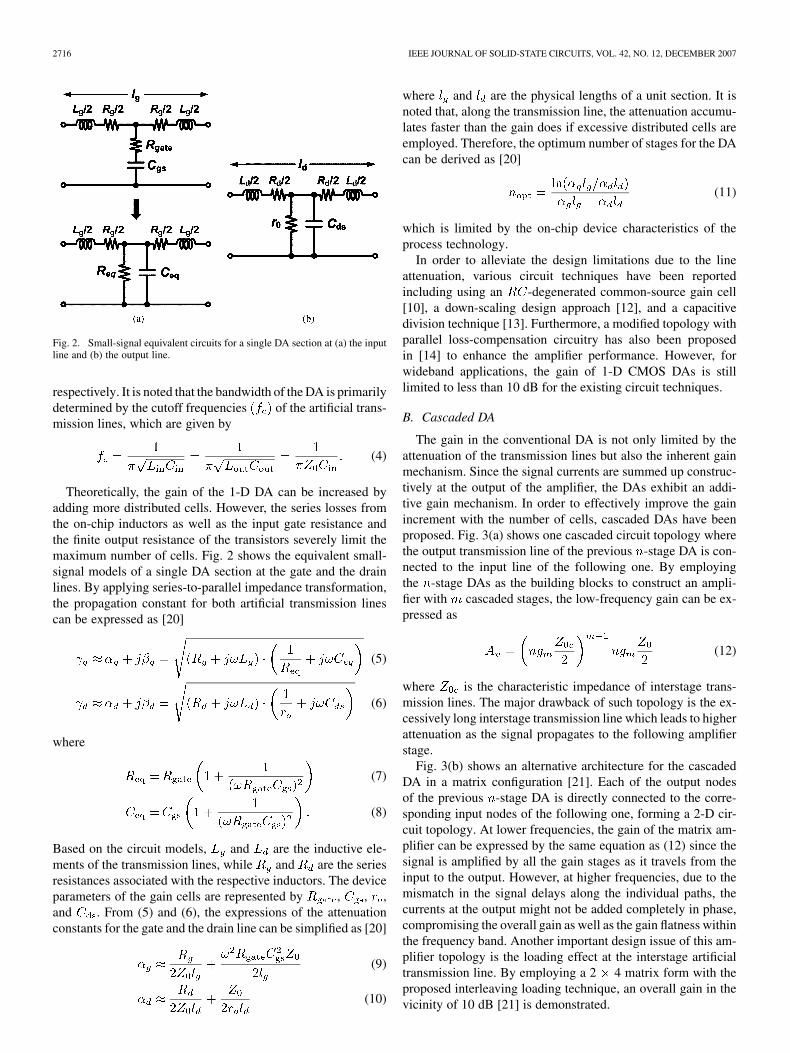
The gain in the conventional DA is not only limited by theattenuation of the transmission lines but also the inherent gainmechanism. Since the signal currents are summed up construc-tively at the output of the amplifier, the DAs exhibit an addi-tive gain mechanism. In order to effectively improve the gainincrement with the number of cells, cascaded DAs have beenproposed. Fig. 3(a) shows one cascaded circuit topology wherethe output transmission line of the previous -stage DA is con-nected to the input line of the following one. By employingthe -stage DAs as the building blocks to construct an ampli-fier with cascaded stages, the low-frequency gain can be ex-pressed as
(12)
where is the characteristic impedance of interstage trans-mission lines. The major drawback of such topology is the ex-cessively long interstage transmission line which leads to higherattenuation as the signal propagates to the following amplifierstage.
Fig. 3(b) shows an alternative architecture for the cascadedDA in a matrix configuration [21]. Each of the output nodesof the previous -stage DA is directly connected to the corre-sponding input nodes of the following one, forming a 2-D cir-cuit topology. At lower frequencies, the gain of the matrix am-plifier can be expressed by the same equation as (12) since thesignal is amplified by all the gain stages as it travels from theinput to the output. However, at higher frequencies, due to themismatch in the signal delays along the individual paths, thecurrents at the output might not be added completely in phase,compromising the overall gain as well as the gain flatness withinthe frequency band. Another important design issue of this am-plifier topology is the loading effect at the interstage artificialtransmission line. By employing a 2 4 matrix form with theproposed interleaving loading technique, an overall gain in thevicinity of 10 dB [21] is demonstrated.
CHIEN AND LU: HIGH-GAIN DISTRIBUTED AMPLIFIERS WITH CASCADED GAIN STAGES IN 0.18- m CMOS 2717
Fig. 3. Circuit schematics of (a) the cascaded DA, (b) the matrix DA, and (c) the CSSDA.
Note that, in most of the cascaded DA topologies, the numberof cascaded stages is typically smaller than that of thedistributed cells along the transmission lines , making thegain primarily determined by the additive mechanism insteadof the multiplicative one. In order to take full advantage ofthe multiplicative gain mechanism, a cascaded single-stagedistributed amplifier (CSSDA) [9], [22]–[24] is proposed asshown in Fig. 3(c). Each amplifier stage is now composed of asingle transistor, a -ladder network to separate the capac-itances, and a termination resistor for impedance matching.Since only multiplicative gain mechanism is involved in thistopology, the gain increment is more effective than any of theother topologies as the number of stages increases. Assumingthat cascaded stages are employed, the low-frequency gainof the CSSDA can be derived as
(13)
where is the impedance of the interstage load. From (13),it is clear that there are three major advantages in terms of gainfor this architecture. First, the gain grows exponentially with thenumber of stages. Second, only one termination load is requiredfor each interstage line. Third, the characteristic impedance ofthe interstage lines does not need to match the 50- impedance.Therefore, it is well suited for high-gain amplifier designs withreasonable power consumption. The drawback of this topology
is that the output power of the amplifier is limited by the devicesize of the output stage [23]. Typically, a larger aspect ratio ofthe transistor results in higher output power at the cost of a de-graded amplifier bandwidth.
C. Proposed Amplifier Architecture
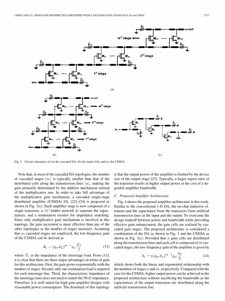
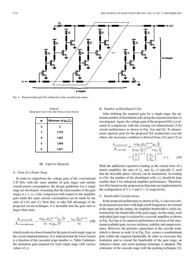
Fig. 4 shows the proposed amplifier architecture in this work.Similar to the conventional 1-D DA, the on-chip inductive el-ements and the capacitance from the transistors form artificialtransmission lines at the input and the output. To overcome thedesign tradeoff between power and bandwidth while providingeffective gain enhancement, the gain cells are realized by cas-caded gain stages. The proposed architecture is considered acombination of the DA as shown in Fig. 1 and the CSSDA asshown in Fig. 3(c). Provided that gain cells are distributedalong the transmission lines and each cell is composed of cas-caded stages, the low-frequency gain of the amplifier is given by
(14)
which shows both the linear and exponential relationship withthe numbers of stages and , respectively. Compared with thecase for the CSSDA, higher output power can be achieved in theproposed architecture without sacrificing the bandwidth as thecapacitances of the output transistors are distributed along theartificial transmission line.
2718 IEEE JOURNAL OF SOLID-STATE CIRCUITS, VOL. 42, NO. 12, DECEMBER 2007
Fig. 4. Proposed high-gain DA architecture with cascaded gain stages.
TABLE IREQUIRED GAIN FOR THE SINGLE GAIN STAGE
III. CIRCUIT DESIGNS
A. Gain of a Single Stage
In order to outperform the voltage gain of the conventional1-D DAs with the same number of gain stages and similaroverall power consumption, the design guidelines for a singlestage are developed. Assuming that the total number of the gainstages is , a fair comparison with respect to the amplifiergain under the same current consumption can be made by theratio of (14) and (1). Note that, to take full advantage of theproposed circuit technique, it is desirable that the gain ratio islarger than unity
(15)
which results in a lower bound for the gain of each single stage inthe circuit implementations. It is indicated that the lower boundis a function of the cascaded stage number . Table I tabulatesthe minimum gain required for each single stage with variousvalues of .
B. Number of Distributed Cells
After defining the required gain for a single stage, the op-timum number of distributed cells along the transmission lines isinvestigated. Again, the voltage gain of the proposed DA is eval-uated in comparison with the existing two-dimensional (2-D)circuit architectures as shown in Fig. 3(a) and (b). To demon-strate superior gain for the proposed DA architecture over theothers, the necessary condition is derived from (14) and (12) as
(16)
With the additional capacitive loading at the central lines of amatrix amplifier, the ratio of and is typically 2, suchthat the desirable phase velocity can be maintained. Accordingto (16), the number of the distributed cells should be keptsmaller than 4 for enhanced amplifier performance. Therefore,two DAs based on the proposed architecture are implemented inthe configuration of 3 3 and 2 4, respectively.
C. Bandwidth Considerations
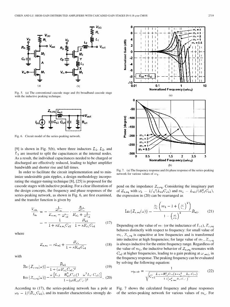
In the proposed architecture as shown in Fig. 4, since two arti-ficial transmission lines with high cutoff frequencies are formedat the input and the output, the amplifier bandwidth is solely de-termined by the bandwidth of the gain stages. In this study, eachindividual gain stage is realized by a cascode amplifier as shownin Fig. 5(a) due to its superior performance in terms of the max-imum available gain, reverse isolation, stability and output resis-tance. However, the parasitic capacitance at the cascode node,which is shown as node A in Fig. 5(a), creates a nondominantpole within the required bandwidth. In order to overcome thislimitation and to extend the bandwidth of the gain stage, aninductive shunt- and series-peaking technique is adopted. Theschematic of the cascode stage with the peaking technique [3],
CHIEN AND LU: HIGH-GAIN DISTRIBUTED AMPLIFIERS WITH CASCADED GAIN STAGES IN 0.18- m CMOS 2719
Fig. 5. (a) The conventional cascode stage and (b) broadband cascode stagewith the inductive peaking technique.
Fig. 6. Circuit model of the series-peaking network.
[9] is shown in Fig. 5(b), where three inductors , , andare inserted to split the capacitances at the internal nodes.
As a result, the individual capacitances needed to be charged ordischarged are effectively reduced, leading to higher amplifierbandwidth and shorter rise and fall times.
In order to facilitate the circuit implementation and to min-imize undesirable gain ripples, a design methodology incorpo-rating the stagger-tuning technique [8], [25] is proposed for thecascode stages with inductive peaking. For a clear illustration ofthe design concepts, the frequency and phase responses of theseries-peaking network, as shown in Fig. 6, are first examined,and the transfer function is given by
(17)
where
(18)
with
(19)
(20)
According to (17), the series-peaking network has a pole at, and its transfer characteristics strongly de-
Fig. 7. (a) The frequency response and (b) phase response of the series-peakingnetwork for various values of m .
pend on the impedance . Considering the imaginary partof with and ,the expression in (20) can be rearranged as
(21)
Depending on the value of (or the inductance of ),behaves distinctly with respect to frequency: for small value of
, is capacitive at low frequencies and is transformedinto inductive at high frequencies; for large value of ,is always inductive for the entire frequency range. Regardless ofthe value of , the inductive behavior of resonates with
at higher frequencies, leading to a gain peaking at inthe frequency response. The peaking frequency can be evaluatedby solving the following equation:
(22)
Fig. 7 shows the calculated frequency and phase responsesof the series-peaking network for various values of . For
2720 IEEE JOURNAL OF SOLID-STATE CIRCUITS, VOL. 42, NO. 12, DECEMBER 2007
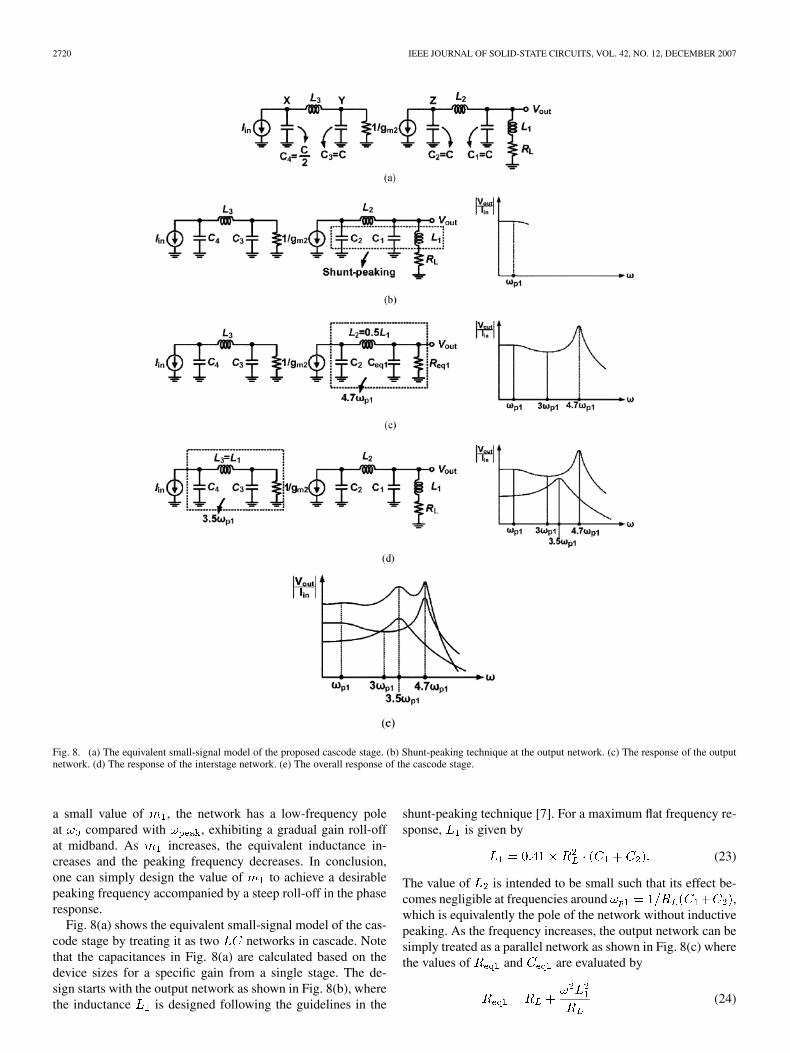
Fig. 8. (a) The equivalent small-signal model of the proposed cascode stage. (b) Shunt-peaking technique at the output network. (c) The response of the outputnetwork. (d) The response of the interstage network. (e) The overall response of the cascode stage.
a small value of , the network has a low-frequency poleat compared with , exhibiting a gradual gain roll-offat midband. As increases, the equivalent inductance in-creases and the peaking frequency decreases. In conclusion,one can simply design the value of to achieve a desirablepeaking frequency accompanied by a steep roll-off in the phaseresponse.
Fig. 8(a) shows the equivalent small-signal model of the cas-code stage by treating it as two networks in cascade. Notethat the capacitances in Fig. 8(a) are calculated based on thedevice sizes for a specific gain from a single stage. The de-sign starts with the output network as shown in Fig. 8(b), wherethe inductance is designed following the guidelines in the
shunt-peaking technique [7]. For a maximum flat frequency re-sponse, is given by
(23)
The value of is intended to be small such that its effect be-comes negligible at frequencies around ,which is equivalently the pole of the network without inductivepeaking. As the frequency increases, the output network can besimply treated as a parallel network as shown in Fig. 8(c) wherethe values of and are evaluated by
(24)
CHIEN AND LU: HIGH-GAIN DISTRIBUTED AMPLIFIERS WITH CASCADED GAIN STAGES IN 0.18- m CMOS 2721
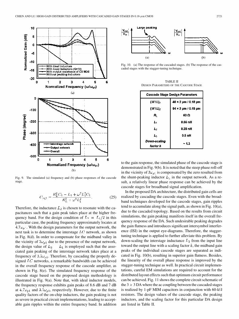
Fig. 9. The simulated (a) frequency and (b) phase responses of the cascodestage.
(25)
Therefore, the inductance is chosen to resonate with the ca-pacitances such that a gain peak takes place at the higher fre-quency band. For the design condition of in thisparticular case, the peaking frequency approximately locates at
. With the design parameters for the output network, thenext task is to determine the interstage network, as shownin Fig. 8(d). In order to compensate for the midband valley inthe vicinity of due to the presence of the output network,the design value of is employed such that the asso-ciated gain peaking of the interstage network takes place at afrequency of . Therefore, by cascading the properly de-signed networks, a remarkable bandwidth can be achievedin the overall frequency response of the cascode amplifier, asshown in Fig. 8(e). The simulated frequency response of thecascode stage based on the proposed design methodology isillustrated in Fig. 9(a). Note that, with ideal inductor models,the frequency response exhibits gain peaks of 8.6 dB and 7 dBat and , respectively. However, due to the finitequality factors of the on-chip inductors, the gain peaking is notas severe in practical circuit implementations, leading to accept-able gain ripples within the entire frequency band. In addition
Fig. 10. (a) The response of the cascaded stages. (b) The response of the cas-caded stages with the stagger-tuning technique.
TABLE IIDESIGN PARAMETERS OF THE CASCODE STAGE
to the gain response, the simulated phase of the cascode stage isdemonstrated in Fig. 9(b). It is noted that the steep phase roll-offin the vicinity of is compensated by the zero resulted fromthe shunt-peaking inductor in the output network. As a re-sult, a relatively linear phase response can be achieved by thecascode stages for broadband signal amplification.
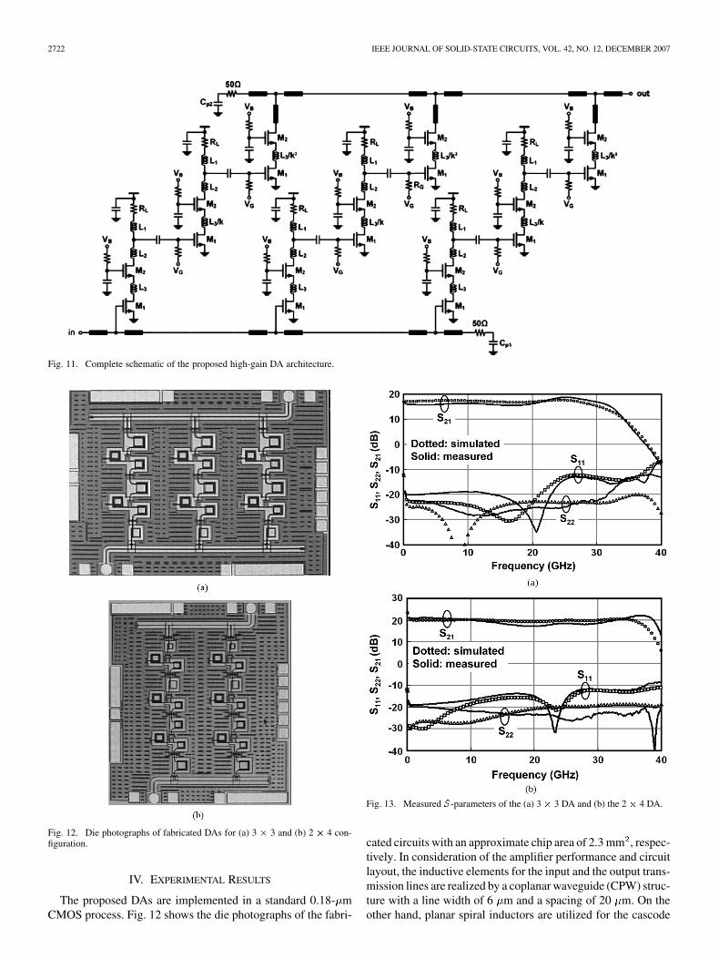
In the proposed DA architecture, the distributed gain cells arerealized by cascading the cascode stages. Even with the broad-band techniques developed for the cascode stages, gain ripplestend to accumulate along the signal path, as shown in Fig. 10(a),due to the cascaded topology. Based on the results from circuitsimulations, the gain peaking manifests itself in the overall fre-quency response of the DA. Such undesirable peaking degradesthe gain flatness and introduces significant intersymbol interfer-ence (ISI) in the output eye-diagrams. Therefore, the stagger-tuning technique is applied to further alleviate this problem. Bydown-scaling the interstage inductance from the input linetoward the output line with a scaling factor , the midband gainpeaks of the individual cascode stages are separated as indi-cated in Fig. 10(b), resulting in superior gain flatness. Besides,the linearity of the overall phase response is improved by thestagger-tuning technique as well. In practical circuit implemen-tations, careful EM simulations are required to account for thedistributed layout effects such that optimum circuit performancecan be achieved. Fig. 11 shows the complete circuit schematic ofthe 3 3 DA where the ac coupling between the cascaded stagesis realized by 1-pF MIM capacitors in conjunction with 60-kresistors. The design values of the cascode stage, the peakinginductors, and the scaling factor for this particular DA designare listed in Table II.
2722 IEEE JOURNAL OF SOLID-STATE CIRCUITS, VOL. 42, NO. 12, DECEMBER 2007
Fig. 11. Complete schematic of the proposed high-gain DA architecture.
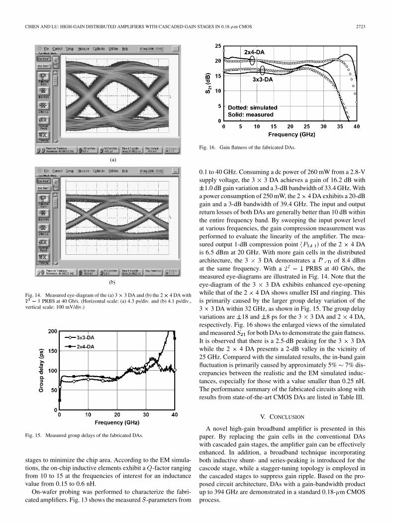
Fig. 12. Die photographs of fabricated DAs for (a) 3 � 3 and (b) 2 � 4 con-figuration.
IV. EXPERIMENTAL RESULTS
The proposed DAs are implemented in a standard 0.18- mCMOS process. Fig. 12 shows the die photographs of the fabri-
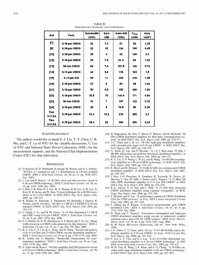
Fig. 13. Measured S-parameters of the (a) 3 � 3 DA and (b) the 2 � 4 DA.
cated circuits with an approximate chip area of 2.3 mm , respec-tively. In consideration of the amplifier performance and circuitlayout, the inductive elements for the input and the output trans-mission lines are realized by a coplanar waveguide (CPW) struc-ture with a line width of 6 m and a spacing of 20 m. On theother hand, planar spiral inductors are utilized for the cascode
CHIEN AND LU: HIGH-GAIN DISTRIBUTED AMPLIFIERS WITH CASCADED GAIN STAGES IN 0.18- m CMOS 2723
Fig. 14. Measured eye-diagram of the (a) 3� 3 DA and (b) the 2� 4 DA with2 � 1 PRBS at 40 Gb/s. (Horizontal scale: (a) 4.3 ps/div. and (b) 4.1 ps/div.,vertical scale: 100 mV/div.)
Fig. 15. Measured group delays of the fabricated DAs.
stages to minimize the chip area. According to the EM simula-tions, the on-chip inductive elements exhibit a -factor rangingfrom 10 to 15 at the frequencies of interest for an inductancevalue from 0.15 to 0.6 nH.
On-wafer probing was performed to characterize the fabri-cated amplifiers. Fig. 13 shows the measured -parameters from
Fig. 16. Gain flatness of the fabricated DAs.
0.1 to 40 GHz. Consuming a dc power of 260 mW from a 2.8-Vsupply voltage, the 3 3 DA achieves a gain of 16.2 dB with
1.0 dB gain variation and a 3-dB bandwidth of 33.4 GHz. Witha power consumption of 250 mW, the 2 4 DA exhibits a 20-dBgain and a 3-dB bandwidth of 39.4 GHz. The input and outputreturn losses of both DAs are generally better than 10 dB withinthe entire frequency band. By sweeping the input power levelat various frequencies, the gain compression measurement wasperformed to evaluate the linearity of the amplifier. The mea-sured output 1-dB compression point of the 2 4 DAis 6.5 dBm at 20 GHz. With more gain cells in the distributedarchitecture, the 3 3 DA demonstrates a of 8.4 dBmat the same frequency. With a PRBS at 40 Gb/s, themeasured eye-diagrams are illustrated in Fig. 14. Note that theeye-diagram of the 3 3 DA exhibits enhanced eye-openingwhile that of the 2 4 DA shows smaller ISI and ringing. Thisis primarily caused by the larger group delay variation of the3 3 DA within 32 GHz, as shown in Fig. 15. The group delayvariations are 18 and 8 ps for the 3 3 DA and 2 4 DA,respectively. Fig. 16 shows the enlarged views of the simulatedand measured for both DAs to demonstrate the gain flatness.It is observed that there is a 2.5-dB peaking for the 3 3 DAwhile the 2 4 DA presents a 2-dB valley in the vicinity of25 GHz. Compared with the simulated results, the in-band gainfluctuation is primarily caused by approximately 5% 7% dis-crepancies between the realistic and the EM simulated induc-tances, especially for those with a value smaller than 0.25 nH.The performance summary of the fabricated circuits along withresults from state-of-the-art CMOS DAs are listed in Table III.
V. CONCLUSION
A novel high-gain broadband amplifier is presented in thispaper. By replacing the gain cells in the conventional DAswith cascaded gain stages, the amplifier gain can be effectivelyenhanced. In addition, a broadband technique incorporatingboth inductive shunt- and series-peaking is introduced for thecascode stage, while a stagger-tuning topology is employed inthe cascaded stages to suppress gain ripple. Based on the pro-posed circuit architecture, DAs with a gain-bandwidth productup to 394 GHz are demonstrated in a standard 0.18- m CMOSprocess.
2724 IEEE JOURNAL OF SOLID-STATE CIRCUITS, VOL. 42, NO. 12, DECEMBER 2007
TABLE IIIPERFORMANCE SUMMARY AND COMPARISON
ACKNOWLEDGMENT
The authors would like to thank E.-J. Lin, T.-Y. Chen, C.-R.Wu, and C.-T. Lu of NTU for the valuable discussions, C. Leeof NTU and National Nano Device Laboratory (NDL) for themeasurement supports, and the National Chip ImplementationCenter (CIC) for chip fabrication.
REFERENCES
[1] D. Kehreer, H.-D. Wohlmuth, H. Knapp, M. Wurzer, and A. L. Scholtz,“40-Gb/s 2:1 multiplexer and 1:2 demultiplexer in 120-nm standardCMOS,” IEEE J. Solid-State Circuits, vol. 38, no. 11, pp. 1830–1837,Nov. 2003.
[2] J. Lee and B. Razavi, “A 40-Gb/s clock and data recovery circuit in0.18-�m CMOS technology,” IEEE J. Solid-State Circuits, vol. 38, no.12, pp. 2181–2190, Dec. 2003.
[3] J. Kim, J.-K. Kim, B.-J. Lee, M.-S. Hwang, H.-R. Lee, S.-H. Lee, N.Kim, D.-K. Jeong, and W. Kim, “Circuit techniques for a 40 Gb/s trans-mitter in 0.13 �m CMOS,” in IEEE ISSCC Dig. Tech. Papers, Feb.2005, pp. 150–151.
[4] K. Kanda, D. Yamazaki, T. Yamamoto, M. Horinaka, J. Ogawa, H.Tamura, and H. Onodera, “40 Gb/s 4:1 MUX/1:4 DEMUX in 90 nmstandard CMOS,” in IEEE ISSCC Dig. Tech. Papers, Feb. 2005, pp.152–153.
[5] U. Singh, L. Li, and M. M. Green, “A 34 Gb/s distributed 2:1 MUXand CMU using 0.18 �m CMOS,” IEEE J. Solid-State Circuits, vol.41, no. 9, pp. 2067–2076, Sep. 2006.
[6] S. S. Mohan, M. D. M. Hershenson, S. P. Boyd, and T. H. Lee, “Band-width extension in CMOS with optimized on-chip inductors,” IEEE J.Solid-State Circuits, vol. 35, no. 3, pp. 346–355, Mar. 2000.
[7] R.-C. Liu, C.-S. Lin, K.-L. Deng, and H. Wang, “Design and analysisof dc-to-14-GHz and 22-GHz CMOS cascode distributed amplifiers,”IEEE J. Solid-State Circuits, vol. 39, no. 8, pp. 1370–1374, Aug. 2004.
[8] B. Analui and A. Hajimiri, “Bandwidth enhancement for trans-impedance amplifiers,” IEEE J. Solid-State Circuits, vol. 39, no. 8, pp.1263–1270, Aug. 2004.
[9] S. Galal and B. Razavi, “40-Gb/s amplifier and ESD protection circuitin 0.18-�m CMOS technology,” IEEE J. Solid-State Circuits, vol. 39,no. 12, pp. 2389–2396, Dec. 2004.
[10] H. Shigematsu, M. Sato, T. Hirose, F. Brewer, and M. Rodwell, “40Gb/s CMOS distributed amplifier for fiber-optic communication sys-tems,” in IEEE ISSCC Dig. Tech. Papers, Feb. 2004, pp. 476–477.
[11] J.-C. Chien and L.-H. Lu, “40 Gb/s high-gain distributed amplifierswith cascaded gain stages in 0.18 �m CMOS,” in IEEE ISSCC Dig.Tech. Papers, Feb. 2007, pp. 538–539.
[12] A. Yazdi, D. Lin, and P. Heydari, “A 1.8 V three-stage 25 GHz 3dB-BW differential non-uniform downsized distributed amplifier,” inIEEE ISSCC Dig. Tech. Papers, Feb. 2005, pp. 156–157.
[13] R.-C. Liu, T.-P. Wang, L.-H. Lu, and H. Wang, “An 80 GHz traveling-wave amplifier in a 90 nm CMOS technology,” in IEEE ISSCC Dig.Tech. Papers, Feb. 2005, pp. 154–155.
[14] K. Moez and M. Elmasry, “A 10 dB 44 GHz loss-compensated CMOSdistributed amplifier,” in IEEE ISSCC Dig. Tech. Papers, Feb. 2007,pp. 548–549.
[15] J. Kim, J.-O. Plouchart, N. Zamdmer, R. Trzcenski, R. Groves, M.Sherony, Y. Tan, M. Talbi, J. Safran, and L. Wagner, “A 12 dBm 320GHz GBW distributed amplifier in 0.12 �m SOI CMOS,” in IEEEISSCC Dig. Tech. Papers, Feb. 2004, pp. 478–479.
[16] R. E. Amaya, N. G. Tarr, and C. Plett, “A 27 GHz fully integratedCMOS distributed amplifier using coplanar waveguides,” in RFICSymp. Dig. Papers, Jun. 2004, pp. 193–196.
[17] P. Heydari and D. Lin, “A performance optimized CMOS distributedLNA for UWB receivers,” in Proc. IEEE Custom Integrated CircuitsConf., Sep. 2005, pp. 337–340.
[18] F. Zhang and P. Kinget, “Low-power programmable gain CMOSdistributed LNA,” IEEE J. Solid-State Circuits, vol. 41, no. 6, pp.1333–1343, Jun. 2006.
[19] X. Guan and C. Nguyen, “Low-power-consumption and high-gainCMOS distributed amplifiers using cascade of inductively coupledcommon-source gain cells for UWB systems,” IEEE Trans. Microw.Theory Tech., vol. 54, no. 8, pp. 3278–3283, Aug. 2006.
[20] D. M. Pozar, Microwave Engineering, 2nd ed. New York: Wiley,1998.
[21] J.-C. Chien, T.-Y. Chen, and L.-H. Lu, “A 9.5-dB 50-GHz matrix dis-tributed amplifier in 0.18-�m CMOS,” in Symp. VLSI Circuits Dig.Tech. Papers, Jun. 2006, pp. 182–183.
[22] C. Lee, L.-C. Cho, and S.-I. Liu, “A 0.1-25.5-GHz differential cas-caded-distributed amplifier in 0.18-�m CMOS technology,” in 2005IEEE Asian Solid-State Circuits Conf., Nov. 2005, pp. 129–132.
[23] M.-D. Tsai, H. Wang, J.-F. Kuan, and C.-S. Chang, “A 70 GHz cas-caded multi-stage distributed amplifier in 90 nm CMOS technology,”in IEEE ISSCC Dig. Tech. Papers, Feb. 2005, pp. 402–403.
CHIEN AND LU: HIGH-GAIN DISTRIBUTED AMPLIFIERS WITH CASCADED GAIN STAGES IN 0.18- m CMOS 2725
[24] M.-D. Tsai, K.-L. Deng, H. Wang, C.-H. Chen, C.-S. Chang, and J.G. J. Chern, “A miniature 25-GHz 9-dB CMOS cascaded single-stagedistributed amplifier,” IEEE Microw. Wireless Compon. Lett., vol. 14,no. 12, pp. 554–556, Dec. 2004.
[25] S. Shekhar, J. S. Walling, and D. J. Allstot, “Bandwidth extension tech-niques for CMOS amplifiers,” IEEE J. Solid-State Circuits, vol. 41, no.11, pp. 2424–2439, Nov. 2006.
Jun-Chau Chien (S’05) was born in Taipei, Taiwan,R.O.C., in 1981. He received the B.S. and M.S.degrees in electronics engineering from NationalTaiwan University, Taipei, in 2004 and 2006,respectively.
His research interests focus on integrated circuitdesigns for high-speed communication systems.
Mr. Chien was a recipient of the 2007 InternationalSolid-State Circuits Conference (ISSCC) SilkroadAward, the 2006 Outstanding Research Award, andthe Annual Best Thesis Award of Graduate Institute
of Electronics Engineering, National Taiwan University.
Liang-Hung Lu (M’02) was born in Taipei, Taiwan,R.O.C., in 1968. He received the B.S. and M.S.degrees in electronics engineering from NationalChiao-Tung University, Hsinchu, Taiwan, R.O.C., in1991 and 1993, respectively, and the Ph.D. degreein electrical engineering from the University ofMichigan, Ann Arbor, in 2001.
During his graduate studies, he was involved inSiGe HBT technology and monolithic microwave in-tegrated circuit (MMIC) designs. From 2001 to 2002,he was with the IBM T. J. Watson Research Center,
Yorktown Heights, NY, where he was involved with low-power and RF inte-grated circuits for silicon-on-insulator technology. In August of 2002, he joinedthe faculty of the Graduate Institute of Electronics Engineering and the De-partment of Electrical Engineering, National Taiwan University, Taipei, wherehe is currently an Associate Professor. His research interests include CMOS/BiCMOS RF and mixed-signal integrated circuit designs.