Embed Size (px)
Citation preview

2684 IEEE TRANSACTIONS ON INDUSTRY APPLICATIONS, VOL. 49, NO. 6, NOVEMBER/DECEMBER 2013
A Thermal Management Approach to Fault-ResilientDesign of Three-Level IGCT-Based NPC Converters
Anderson Vagner Rocha, Hélder de Paula, Manoel Eustáquio dos Santos, and Braz J. Cardoso Filho
Abstract—The three-level (3L) neutral-point-clamped (NPC)converter, introduced by Nabae in 1981, has become the mostpopular converter topology for high-power medium-voltage in-dustrial drives. Responsible for driving key processes in variousindustries, high availability of these converters is mandatory, sincetheir maintenance or replacement implies downtimes incompat-ible with the requirements of the production processes. In thiscontext, this paper discusses a thermal management approachto a fault-resilient design of the 3L integrated gate-commutatedthyristor-based NPC converters. The main goal is to reduce thedamage extension and restrict the damage pattern within the NPCbridge in case of failures or malfunction of currently employedprotection schemes. It is shown that the thermal stress caused bythe short-circuit currents can be managed, easing the selectivityand tracing of the damaged components, thus reducing the overallconverter downtime and maintenance costs.
Index Terms—Active front end (AFE), integrated gate-commutated thyristor (IGCT), medium-voltage (MV) powerconverter, multilevel converters, neutral point clamped (NPC),protection, reliability.
I. INTRODUCTION
THE three-level (3L) converter with neutral point clamped(NPC) was introduced by Nabae in 1981 [1] and is cur-
rently the most popular topology for medium-voltage (MV)converters used in industrial drives, being commercialized bymajor manufacturers worldwide [2], [3]. Currently, both theintegrated gate-commutated thyristor (IGCT) and insulated-gate bipolar transistor (IGBT) can be used, with no seriesconnections, as self-commutated switches in the multilevelMV converters. The IGCTs are more advantageous for higherpowers due to their lower on-state voltage drop and snubberlessoperation capability, resulting in highly efficient and reliableMV converter systems with minimum part count [4], [5].
Manuscript received December 13, 2012; revised March 28, 2013;accepted March 31, 2013. Date of publication June 3, 2013; date of cur-rent version November 18, 2013. Paper 2012-IPCC-627.R1, presented at the2012 IEEE Energy Conversion Congress and Exposition, Raleigh, NC, USA,September 15–20, and approved for publication in the IEEE TRANSACTIONS
ON INDUSTRY APPLICATIONS by the Industrial Power Converter Committeeof the IEEE Industry Applications Society.
A. V. Rocha is with the Department of Electrical Engineering, UniversidadeFederal de Minas Gerais, Belo Horizonte 31270-010, Brazil, and also withthe Centro Federal de Educação Tecnológica de Minas Gerais, Belo Horizonte30421-169, Brazil (e-mail: [email protected]).
H. de Paula and B. J. Cardoso Filho are with the Department of Elec-trical Engineering, Universidade Federal de Minas Gerais, Belo Horizonte31270-010, Brazil (e-mail: [email protected]; [email protected]).
M. E. dos Santos is with the Management of Engineering, Gerdau AçominasS/A, Ouro Branco 36420-000, Brazil (e-mail: [email protected]).
Color versions of one or more of the figures in this paper are available onlineat http://ieeexplore.ieee.org.
Digital Object Identifier 10.1109/TIA.2013.2265935
TABLE ISUMMARY OF THE MV IGCT-BASED NPC CONVERTERS
MARKETED BY MAJOR DRIVE MANUFACTURERS
Fig. 1. Circuit configuration of a 3L NPC converter.
Table I shows the current power ratings and semiconductortypes adopted by some of the major NPC IGCT-based variable-frequency drive (VFD) manufacturers in the world [5].
A schematic of a three-phase MV 3L NPC IGCT-basedconverter is presented in Fig. 1. The topology in Fig. 1 can beused as an inverter or as an active front-end (AFE) converter.The 3L NPC topology traditionally has been used for MVdrives in industrial and other applications. Such large drivesare typically responsible for driving key processes in variousindustries. As a consequence, high availability of these con-verters is mandatory, since their maintenance or replacementimplies downtimes incompatible with the requirements of theproduction processes.
MV converters should be tolerant to any kind of failure, sincethey are present in many mission-critical industrial systems.Fault tolerance in high-power converters is difficult to achieve.A more realistic and desirable characteristic is that, followinga failure, the converter is restored to normal operation in a fastand economical way. This can be achieved from intrinsic dam-age control capability. In this context, the term fault resilient isused to characterize equipment with such characteristic.
This paper discusses a fault-resilient design of the 3L IGCT-based NPC AFE converters, based on a thermal managementapproach. The main goal is to reduce the damage extensionand restrict the damage pattern in the AFE converter in caseof failures or malfunction of the firing mode protection scheme[13], a widely used solution for protection of IGCT-based
0093-9994 © 2013 IEEE

ROCHA et al.: APPROACH TO FAULT-RESILIENT DESIGN OF THREE-LEVEL IGCT-BASED NPC CONVERTERS 2685
Fig. 2. Block diagram of a typical regenerative IGCT-based NPC VFD.
converters. It is shown that the thermal stress caused by theshort-circuit currents from the firing mode protection can bemanaged, preserving the costly components, easing both theselectivity and tracing of the damaged parts. The target benefitshere are the reduction of the overall downtime and maintenancecosts.
II. REGENERATIVE VFD SYSTEM DESCRIPTION
A. Typical Arrangement With Regeneration Capability
Nowadays, aiming to meet technical and economical re-quirements, the modern high-capacity equipment in productionplants typically employ large-horsepower squirrel-cage induc-tion motors fed by MV inverters. In its simplest form, 3L MV-VFD along with the related protection device comprises aninput transformer, a circuit breaker or fuses, two converters(active rectifier and inverter), and an induction motor, as shownin Fig. 2. This configuration, based on two structurally identicalconverters (as shown in Fig. 1), is the typical choice when alarge independent drive with breaking requirement is needed.
In this configuration, the operation in the regenerative modeis guaranteed due to the NPC active rectifier. This feature isvery attractive for applications such as belt conveyors with longdownhill runs, rolling mills, large excavators, hydrotransport,and cranes.
The VFD illustrated in Fig. 2 uses a combination ofpulsewidth-modulated rectifier and inverter to control the motorspeed and torque. A power transformer is used to reduce thevoltage from the power grid level (typically 13.8 kV and higher)to the drive rated voltage, typically 2.3 or 4.16 kV. In the VFD,the ac incoming power is rectified by the NPC IGCT-basedactive rectifier and transmitted internally along busbars. Thisdc power is then fed to the NPC inverter shown in Fig. 2. TheNPC inverter converts the dc power back to ac power, with theIGCTs being controlled to produce a varying frequency-varyingvoltage output to meet the motor requirements and properlydrive the mechanical load. The fundamental frequency of theVFD output voltage essentially determines the speed of theload. Proper variation of the output frequency and voltage ofthe VFD sets the rate of acceleration of the load from start up.Significant heat is generated during the operation of the VFDso a water cooling system may be incorporated within the VFDcabinets to draw off heat from various sections of the drive.
In most commercial solutions, the VFD system is providedwith a circuit breaker installed upstream from the VFD trans-former, which is adjusted to trip in the event of a fault beingdetected in the VFD and to protect the VFD from furtherdamage. In some industrial plants, this circuit breaker may
TABLE II4 MVA VFD SYSTEM DATA
Fig. 3. NPC phase leg with the clamp circuit for freewheeling diode di/dtturn-off limitation.
be the one and only protection element against severe faultsin the VFD.
B. VFD Characterization
For the purposes of this study, a regenerative VFD employingcommercial converters able to drive a 4125-hp induction motorin 2300 V from a 23-kV power grid was considered. Table IIshows the main data of the drive system. Other important dataincluding the information obtained from the semiconductormanufacturers’ datasheet are shown in the Appendix.
C. Clamp Circuit for Freewheeling Diodes
With the development of the IGCT, many of the problemsrelated to the limitations in the gate turn-off thyristor (GTO)switching performance were solved. Turn-off snubbers are nolonger required, but limiting di/dt at turn-on is still necessaryto keep the diode’s reverse recovery process within its safeoperating area [9].
Due to its thyristor nature, the GCT does not provide intrinsicdi/dt control. Instead, the di/dt at turn-on is limited by meansof an inductor (Lcl), clamped by a diode (Dcl) and a resistorplaced in the dc bus. This di/dt snubber also limits the rateof rise of the dc bus current in the event of a shoot-through.Details of the di/dt snubber circuit for the freewheeling diodeare shown in Fig. 3 for both rectifier and inverter NPC bridges.The snubber component data for the NPC rectifier and inverterbridges (taken from a commercial drive with ratings similar tothe one considered in this paper) are presented in Table III.
2686 IEEE TRANSACTIONS ON INDUSTRY APPLICATIONS, VOL. 49, NO. 6, NOVEMBER/DECEMBER 2013
TABLE IIIPASSIVE ELEMENT VALUES FOR CLAMP DEVICE CIRCUIT
III. OVERCURRENT PROTECTION IN REGENERATIVE
IGCT-BASED NPC CONVERTERS
Despite the numerous advantages of using MV VFDs inseveral applications, special attention should be given to theprotection schemes of the power converters. When a faultoccurs in a VFD, if the protection scheme does not operateproperly, the converter can be seriously damaged, requiring along time for its repair or replacement. In this case, the financiallosses due to the extended downtime will be dramatic [7].
The protection strategy of high-power NPC IGCT-based con-verters plays a vital role in ensuring the availability of the drive.Due to their thyristor-type nature, the IGCTs are not capable ofturning off high currents, such as those resulting from a short-circuit condition. Therefore, the overcurrent protection schemeis one of the most important points related to the IGCT-basedpower converter reliability [8], [11].
In commercial drives with AFE, the overcurrent protectionstrategy takes advantage of the inherent overload capability ofthe IGCTs. When a fault is detected, the protection is typicallyprovided by turning on all IGCTs in the converter to limit thethermal stresses on each device due to the energy in the dcbus capacitors and power mains. In the case of AFE, the faultyconverter needs to be quickly disconnected from the mains, lim-iting the total energy dissipated in the power devices. The ap-propriate sizing of the power devices guarantees their integrityas long as the breaker device works properly. This interestingprotection philosophy is known as firing mode protection, andits success is subjected to the proper and timely operation of thebreaker element (fast circuit breaker or fuses) upon the eventof a fault. After the firing protection is initiated, the energystored in the dc-link capacitors is dissipated in most of theconverter power devices, while the energy from the ac mainsis restricted to the AFE. It was shown in [6] that the activerectifier survival is completely dependent on the clearing timeto interrupt the short-circuit currents. In other words, a fault inany of the converters of the VFD and triggering of the firingmode protection, followed by a misoperation of the breakerdevice, can result in irreversible damages to the AFE increasingthe repair costs and the drive downtime.
The fuseless converters are designed to operate safely with-out fuses employing fast circuit breakers with clearing times ofabout 70 ms. Unlike a fuse, the circuit breaker can be remotelyreset to resume normal operation, resulting in less spare partsand better overall availability. In [8], it was shown that, in ashort-circuit situation, the fuse with the required i2t to protectthe IGCTs has a rated current lower than the converter rated cur-rent. As a result, such fuse may blow in situations which are notactually faults. The conclusion is that the protection with fusesrequires oversizing the IGCTs and diodes, leading to highercost and poor silicon utilization. All the aforementioned argu-ments support the use of fast circuit breakers as the mains dis-connecting devices in commercial MV IGCT-based converters.
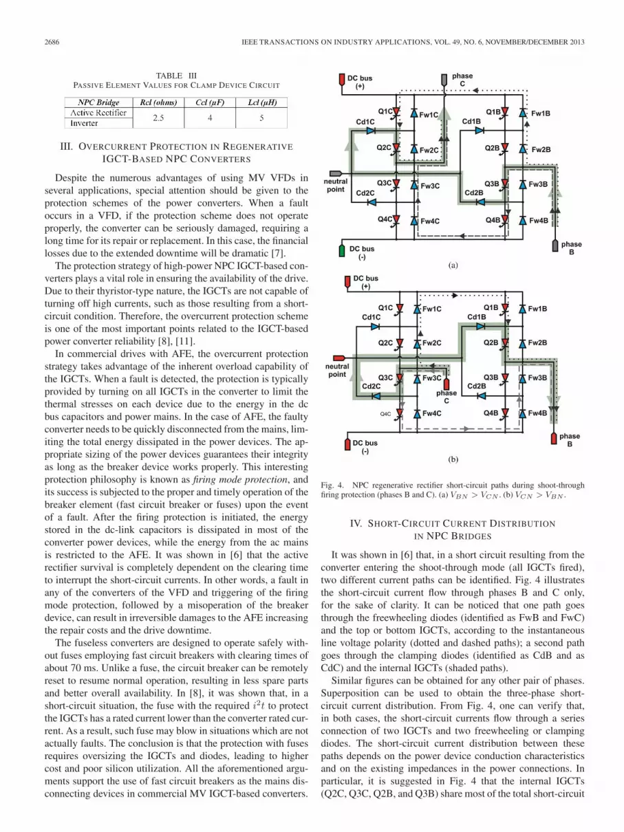
Fig. 4. NPC regenerative rectifier short-circuit paths during shoot-throughfiring protection (phases B and C). (a) VBN > VCN . (b) VCN > VBN .
IV. SHORT-CIRCUIT CURRENT DISTRIBUTION
IN NPC BRIDGES
It was shown in [6] that, in a short circuit resulting from theconverter entering the shoot-through mode (all IGCTs fired),two different current paths can be identified. Fig. 4 illustratesthe short-circuit current flow through phases B and C only,for the sake of clarity. It can be noticed that one path goesthrough the freewheeling diodes (identified as FwB and FwC)and the top or bottom IGCTs, according to the instantaneousline voltage polarity (dotted and dashed paths); a second pathgoes through the clamping diodes (identified as CdB and asCdC) and the internal IGCTs (shaded paths).
Similar figures can be obtained for any other pair of phases.Superposition can be used to obtain the three-phase short-circuit current distribution. From Fig. 4, one can verify that,in both cases, the short-circuit currents flow through a seriesconnection of two IGCTs and two freewheeling or clampingdiodes. The short-circuit current distribution between thesepaths depends on the power device conduction characteristicsand on the existing impedances in the power connections. Inparticular, it is suggested in Fig. 4 that the internal IGCTs(Q2C, Q3C, Q2B, and Q3B) share most of the total short-circuit

ROCHA et al.: APPROACH TO FAULT-RESILIENT DESIGN OF THREE-LEVEL IGCT-BASED NPC CONVERTERS 2687
Fig. 5. Charging proccess of the dc-link capacitors.
current, and therefore, they are the first candidates to fail due tothe thermal stresses.
V. THERMAL BEHAVIOR OF THE POWER DEVICES
IN THE FIRING PROTECTION MODE
A. Thermal Stresses in the Power Devices
As the firing protection mode is initiated, the power semicon-ductors in the VFD devices are subjected to a sequence of twodifferent thermal stress modes:
1) the transient thermal stress due to the dc-link capacitordischarge in both converters;
2) the permanent thermal stress due to the short-circuitcurrent from the power grid in the active rectifier.
The effects of the phenomena aforementioned were inves-tigated on simulation models implemented in Matlab/Simulinkand Ansoft Simplorer softwares. It was verified that the temper-atures in the junctions of the power devices dangerously start toincrease compared to the normal operation of the converters.
In the event of a fault in any of the VFD converters, theprotection scheme is expected to disconnect the converter fromthe mains in a very short time: 70 ms or less. Despite thecommanded shoot-through, the proper drive design ensures thatno power devices will be damaged. If the converter circuitbreaker does not open for any reason, the upstream protectionmust actuate. According to international standards, the inputtransformer and reactor are able to withstand short-circuit cur-rents for at least 2 s [10] implying that the short-circuit currentsmust be interrupted within a 2-s interval.
B. DC-Link Capacitor Discharging Process
The results from keeping the VFD converters in firing protec-tion mode for 2 s were simulated, aiming to observe the thermaleffects on the temperatures of the power devices. The chargingand discharging processes of the dc-link capacitors are depictedin Figs. 5 and 6, respectively. The shoot-through command wassent to the IGCTs in both converters after about 50 ms fromthe drive power up. The dc-link capacitors are fully chargedin about 4 ms. The discharge is followed by an oscillationcaused by the resonance between the dc-link capacitors and theinductance from the snubber circuits.
The oscillatory nature of the dc bus capacitor dischargingcurrent can be explained with the aid of the equivalent circuitshown in Fig. 7 considering the converters in the shoot-through
Fig. 6. Discharging process of the dc-link capacitors during the firing protec-tion mode.
Fig. 7. Equivalent dc bus discharging network on the shoot-through firingmode protection.
Fig. 8. Total discharge dc-link capacitor current.
mode (all IGCTs fired). The amplitude of the first pulse and thedischarge current damping depend on the conduction character-istics of the components, busbar impedances, and connectionsin the converters. The oscillation frequency (fo) is determinedaccording to
fo =1
2 · π ·√
Leq · Ceq
(1)
where Leq is the equivalent inductance in the bridge dischargingcircuit and Ceq is the equivalent series capacitance of the dclink. From the parameters in Tables II and III for Lcl and C, theobtained fo is 1125 Hz. The correspondent period To is about0.9 ms.
The capacitor discharging process takes about 15 ms as canbe seen in Fig. 8 for the considered drive.
It is shown in Fig. 8 that the total transient current io throughthe capacitors reaches a peak of 117 kA and is extinguished

2688 IEEE TRANSACTIONS ON INDUSTRY APPLICATIONS, VOL. 49, NO. 6, NOVEMBER/DECEMBER 2013
Fig. 9. Discharge dc-link capacitor current and its components.
Fig. 10. Inverter phase A upper device discharge current.
in about 15 ms. This current is initially shared between thetwo converters and then distributed between the componentsof each NPC bridge. The total discharge current (io) and itscomponents through the power converters (ior and ioi) aredetailed shown in Fig. 9.
C. Semiconductor Transient Thermal Stress
Considering that the two converters are identical, the follow-ing plots show the effects of the dc-link capacitor dischargecurrent in the phase A upper devices (Q1A, Q2A, Fw1A,and Fw2A). The similar effects can be observed in phases Band C. The phase A upper device transient currents are shownin Fig. 10.
The energy losses and junction temperature increase for eachdevice were computed assuming the initial junction temperatureof 100 ◦C. The power device transient thermal impedance frommanufacturer datasheet was considered in the models. Thefollowing set of plots (Figs. 11–13) show the dissipated power,Pj (in kilowatts), energy losses (in joules), and temperatureincrease due to the dc bus capacitor discharge in the inverterpower devices.
Aiming to study the effect of the first current surge on thepower devices, the total thermal energy related to the shoot-through surge current was compared to the test conditionsprovided by the manufacturers. The maximum peak surge on-state current and the limiting load integral (i2t) for standardsinusoidal current pulses are shown in the Appendix. In Figs. 14and 15, Pjlim and Wlim are the computed values for powerand energy losses considering the boundaries provided by thepower device manufacturers. The test conditions assumed in thedatasheets consider sinusoidal pulses of 10 ms for all devicesand 1 ms for the fast power diodes.
Fig. 11. Inverter diodes: Power losses and energy during dc capacitor dis-charge. (a) Phase A freewheeling diode Fw1A. (b) Phase A freewheeling diodeFw2A.
Fig. 12. Inverter IGCTs: Power losses and thermal energy during dc capacitordischarge.
Fig. 13. Inverter Phase A devices—junction temperature increase.
As shown in Fig. 15(b), the rising rate of the thermal en-ergy in the IGCT due to the surge current exceeds the limitguaranteed by the manufacturer. The shortest pulse provided bythe manufacturer for a 56-kA peak surge current in the IGCTsis 3 ms. Since the discharge transient is shorter than that,one cannot conclude on the integrity of the device under suchconditions.

ROCHA et al.: APPROACH TO FAULT-RESILIENT DESIGN OF THREE-LEVEL IGCT-BASED NPC CONVERTERS 2689
Fig. 14. Freewheeling diode power and energy losses in the transient dc busdischarge.
Fig. 15. IGCT power and energy losses in the transient dc bus discharge.(a) Power losses: Datasheet test conditions and simulated results. (b) Energylosses: Datasheet test conditions and simulated results.
D. Permanent Thermal Stress During Firing Protection
The consequences of keeping the converter in the shoot-through mode for 2 s or more, which would occur as a resultof a failure in the breaker element, are shown in Fig. 16 for thephase A devices. From this figure, it can be concluded that, ifthe converter remains connected to the mains after the firingprotection command, the thermal energy in the power deviceswill reach extremely high levels, exceeding their thermal capa-bility and causing a permanent failure of the power converter.This figure confirms that it is possible that the first device to failis one of the internal IGCTs, as discussed in Section IV. Thissituation results from the current path through the clampingdiodes (shaded paths in Fig. 4). The conduction characteristicsof the connections of the clamping diodes may be varied tochange the distribution of the short-circuit currents in the NPCbridge. The goal is to prevent the short-circuit current fromflowing through the clamping diodes, thus avoiding prohibitivecurrents in the internal IGCTs.
Fig. 16. Junction temperature rises on shoot-through mode—Phase A devices.
Fig. 17. Insertion of the resilience impedances (Zr) in the clamping diodebranches of the 3L NPC IGCT-based converter.
VI. MANAGING THE POWER DEVICE THERMAL
STRESS UNDER FIRING PROTECTION
If the converter is in the firing protection mode, the short-circuit current component through the internal IGCTs can bereduced by adding “resilience impedances” (Zr) to the clamp-ing diode connections, as shown in Fig. 17.
Increasing the voltage drop in the clamping diode branches,we can ensure that the first devices to reach their thermal energylimits will always be the freewheeling diodes. As can be seen inFig. 3 (Section IV), the short-circuit current component flowingthrough internal IGCTs (IQ) is higher than the one flowingthrough the freewheeling diodes (IFw). Fig. 18 illustrateshow the IQ/IFw ratio can be changed by choosing properconduction characteristics for the NPC bars. In this picture,the forward resistances of the clamp (RC) and freewheeling(RF ) diode branches are normalized with respect to the IGCTforward resistance (RQ). In the converter design, the ratio

2690 IEEE TRANSACTIONS ON INDUSTRY APPLICATIONS, VOL. 49, NO. 6, NOVEMBER/DECEMBER 2013
Fig. 18. Internal IGCT and power diode short-circuit ratio in terms of theconduction characteristics of the devices.
Fig. 19. Junction temperature rises on shoot-through mode—Phase A devicesof the resilient converter.
IQ/IFw is set for proper thermal stress distribution, the ratioRF/RQ is a circuit parameter, and the ratio RC/RF is thecontrolled variable.
The results presented in Fig. 19 were obtained assumingclamp diode branches with increased resistance (RC = rCd +rbus + Zr).
It is shown in Fig. 19 that the thermal energy in the IGCTs isnow closer to the energy levels in the freewheeling diodes. Theimmediate result of reducing the ratio IQ/IFw is changing thefailure sequence in the NPC bridge. Now, the power diodes arethe first components to fail. It is important to stress here thatpress pack devices used in MV converters always fail shorted,so when they fail, they inherently protect their correspondentantiparallel device; this situation is shown in Fig. 20.
VII. CONCLUSION
In this paper, the short-circuit behavior of the IGCT-basedhigh-power 3L NPC topology has been addressed from the
Fig. 20. Junction temperature rises on shoot-through mode—Phase A failuresequence on thermal stress.
TABLE IVPOWER SEMICONDUCTOR DATA
perspective of characterization of the damage pattern resultingfrom a shoot-through mode followed by a protection schememalfunction. In order to keep the cost to repair at its minimumunder these conditions, it is mandatory to limit the damageto the power diodes as much as possible. The progressionof the damage of the power semiconductors is determinedthrough computer simulations considering the transient ther-mal management of the stressed devices. It is pointed that,by proper design of the converter busbars and managementof the thermal stresses, it is possible for the IGCTs to sur-vive the converter shoot-through mode even in the eventthat the circuit breaker fails to operate. Other immediateconsequence of this proposal is the reduction of the drivetime to repair with a consequent increase in its availabilitysince the selectivity of the damaged components in the caseof catastrophic failures allows faster tracing of items to bereplaced.
APPENDIX
The semiconductor manufacturers’ datasheet is shown inTable IV.

ROCHA et al.: APPROACH TO FAULT-RESILIENT DESIGN OF THREE-LEVEL IGCT-BASED NPC CONVERTERS 2691
REFERENCES
[1] A. Nabae, I. Takahasai, and H. Akagi, “A new neutral-point-clampedPWM inverter,” IEEE Trans. Ind. Appl., vol. IA-17, no. 5, pp. 518–523,Sep. 1981.
[2] D. Floricau, E. Floricau, and G. Gateau, “Three-level active NPC con-verter: PWM strategies and loss distribution,” in Proc. IEEE IECON,Nov. 2008, pp. 3333–3338.
[3] J. Rodrıíguez, J. Lai, and F. Peng, “Multilevel inverters: A survey oftopologies, controls and applications,” IEEE Trans. Ind. Electron., vol. 49,no. 4, pp. 724–738, Aug. 2002.
[4] E. P. Wiechmann, P. Aqueveque, R. Burgos, and J. Rodriguez, “On the effi-ciency of voltage source and current source inverters for high power drives,”IEEE Trans. Ind. Electron., vol. 55, no. 4, pp. 1771–1782, Apr. 2008.
[5] B. Wu, High-Power Converters and AC Drives. Hoboken, NJ, USA:Wiley-IEEE Press, 2006.
[6] A. V. Rocha, G. J. França, M. E. dos Santos, H. de Paula, andB. J. Cardoso Filho, “Improving the performance of protection schemes inthree level IGCT-based neutral point clamped converters,” in Proc. IEEEECCE, Sep. 12–16, 2010, pp. 2326–2332.
[7] A. V. Rocha, G. J. Franca, M. E. dos Santos, H. de Paula, andB. J. Cardoso Filho, “Increasing long belt-conveyors availability by usingfault-resilient medium voltage AC drives,” in Conf. Rec. IEEE IAS Annu.Meeting, Oct. 9–13, 2011, pp. 1–8.
[8] M. E. dos Santos and B. J. Cardoso Filho, “Short circuit and overcurrentprotection of IGCT-based three-level NPC inverters,” in Proc. 35th Annu.IEEE PESC, 2004, vol. 4, pp. 2553–2558.
[9] P. K. Steimer, H. E. Gruening, J. Werninger, E. Carroll, S. Klaka, andS. Linder, “IGCT—A new emerging technology for high power, low costinverters,” IEEE Ind. Appl. Mag., vol. 5, no. 4, pp. 12–18, Jul./Aug. 1999.
[10] Power Transformers—Part 5: Ability to Withstand Short Circuit, IEC Std.60 076-5, 2006, ed.3.0.
[11] A. V. Rocha, G. J. França, M. E. dos Santos, H. de Paula, andB. J. Cardoso Filho, “A fault-resilient implementation of three level NPCIGCT-based converters,” Eletrônica Potência, SOBRAEP Mag., vol. 16,no. 2, pp. 168–176, 2011.
[12] B. M. Hoosh, R. Zaimeddine, and T. M. Undeland, “Comparison of har-monics and common mode voltage in NPC and FLC multilevel convert-ers,” in Proc. 14th Int. EPE/PEMC, Sep. 6–8, 2010, pp. T2-158–T2-161.
[13] ACS 6000 Medium Voltage Drive—Course G750: Operation and Mainte-nance, ABB, Turgi, Switzerland, 2003.
Anderson Vagner Rocha was born in Belo Hori-zonte, Brazil, on February 13, 1970. He received theB.S. degree in electrical engineering from the CentroFederal de Educação Tecnológica de Minas Gerais(CEFET-MG), Belo Horizonte, in 1994 and the M.S.degree in electrical engineering from the Universi-dade Federal de Minas Gerais, Belo Horizonte, in1997, where he is currently working toward the Ph.D.degree in power electronics.
Since 1992, he has been a Faculty Member withCEFET-MG, where he teaches courses on electrical
machines and drives. Currently, his main research interests include medium-voltage ac drives, power semiconductors, efficiency, reliability, and availabilityof high-power converters and their applications.
Hélder de Paula was born in Uberlândia, Brazil,on December 27, 1975. He received the B.S., M.S.,and Ph.D. degrees in electrical engineering fromthe Universidade Federal de Uberlândia, Uberlândia,Brazil, in 1998, 2001, and 2005, respectively.
Since 2006, he has been with the Departmentof Electrical Engineering, Universidade Federal deMinas Gerais, Belo Horizonte, Brazil, as a Professorand a Member of the Tesla Power Engineering Lab-oratory. He has been working on R&D projects onequipment modeling for high-frequency studies. His
main interests are motor drives, electromagnetic compatibility, and dc systems.
Manoel Eustáquio dos Santos was born in Pompéu,Brazil, on September 27, 1953. He received theB.S.E.E. degree from the Pontifícia UniversidadeCatólica de Minas Gerais, Belo Horizonte, Brazil,in 1978 and the M.S. and Ph.D. degrees in electri-cal engineering from the Universidade Federal deMinas Gerais, Belo Horizonte, in 1990 and 2005,respectively.
Since 1981, he has been a Technical Consultantwith Gerdau Açominas S/A (an integrated steel mill),Ouro Branco, Brazil. His current research and tech-
nical interests are in electrical power systems, utility applications of power elec-tronics, high-power converters and drives, and semiconductor power devices.
Braz J. Cardoso Filho was born in Fortaleza, Brazil,on April 21, 1965. He received the B.S. and M.S. de-grees in electrical engineering from the UniversidadeFederal de Minas Gerais (UFMG), Belo Horizonte,Brazil, in 1987 and 1991, respectively, and the Ph.D.degree in electrical engineering from the Universityof Wisconsin, Madison, WI, USA, in 1998.
Since 1989, he has been a Faculty Member withthe Department of Electrical Engineering, UFMG,where he is a Cofounder and the Director of theIndustry Applications Laboratory. He has worked in
the fields of power converters, electric drives, and utility applications of powerconverters and is the author or coauthor of over 100 technical papers publishedin journals and conference proceedings. His main interests are power electronicconverters and their applications in industry and in the power grid, electricmachines and drives, and power semiconductor devices.


