Embed Size (px)
Citation preview

Chapter 24. Nano-Materials and Electronic Devices
24-1
Nano-Materials and Electronic Devices
Academic and Research Staff Professor Jing Kong
Postdoctoral Students Jikang Yuan
Graduate Students Hootan Farhat, Mario Hofmann, Daniel Nezich, Alfonso R. Reina Cecco, Hyungbin Son
Technical and Support Staff Evan Moran
The RLE Nano-materials and Electronics Group pursues investigations of a variety of nanomaterials such as carbon nanotubes, graphene and nanowires, studying their synthesis and integration, electrical and optical characterizations. Chemical vapor deposition method is used for carbon nanotube and graphene synthesis and hydrothermal method is used for the nanowire synthesis. Resonant Raman spectroscopy, electroluminescent and photo-luminescent studies, and photocurrent mapping techniques are used to investigate the electrical and optical properties of these devices. 1. Substrate-Induced Raman Frequency Variation for Single-Walled Carbon Nanotubes Sponsor MIT Project Staff H. Son, J. Kong Collaborating with Y. Zhang, J. Zhang, and Z. Liu at Peking University
During the past few years, resonant Raman spectroscopy has been developed into a powerful tool for characterizing the structure of carbon nanotubes.1 Particularly, it was demonstrated that by comparing the experimental resonant energy Eii and the radial-breathing mode (RBM) frequency ωRBM with the theoretically calculated Kataura plot, it is possible to determine the chirality (n,m) of an individual single-walled nanotube (SWNT).2 As these values can be significantly affected by the surrounding environment of a SWNT, to ensure the accuracy of the chirality identification, it is very important to find out how various environmental conditions alter the Eii or ωRBM values. Recent studies have shown that the ωRBM values are relatively insensitive to the type of wrapping agents surrounding the nanotube in a solution.3 Various calculations have predicted changes in the electronic band structure of nanotubes under strain.4 Raman frequency shifts due to applied uniaxial strain have also been observed.5 Another important source of perturbation is the van der Waals interactions with the substrate. However, it is still an open question to what extent these interactions will affect the SWNT’s Eii or ωRBM.
Figure 1: (a) Schematic illustration for a SWNT lying on a patterned SiO2 substrate. Our samples have various trench widths. All the data presented here are from nanotubes lying over the 3 µm wide trenches. (b) SEM image of the ultralong carbon nanotube sample used for the Raman investigations. (c) High-resolution SEM image of one SWNT lying over the trenches. (In the SEM image, lighter color indicates the trench.)

Chapter 24. Nano-Materials and Electronic Devices
24-2 RLE Progress Report 149
In this paper, we report on the frequency shift of the Raman spectra taken at different locations along the same SWNT, showing different results when the SWNT is freely suspended or when interacting with the substrate. The substrates used in this study are silicon wafers with thermal oxide on the surface, which contains trenches (300 nm deep, 1-80 µm wide) fabricated by photolithography and dry etching (Figure 1). Well separated, individual long SWNTs with a controlled orientation were grown by catalytic chemical vapor decomposition (CVD) of ethanol6 (see Supporting Information for details). An SEM image of the carbon nanotubes thus obtained is shown in Figure 1b. As shown by atomic force microscopy (AFM), nanotubes are suspended over trenches narrower than 3 µm (see Figure 1c and Figure S1).
Raman spectra of the same SWNTs were collected and compared as the laser beam moved along the nanotube. With an excitation energy of 1.96 eV (633 nm), all the SWNTs that came into resonance demonstrated a stronger signal for the suspended part than the part sitting on the SiO2 surface, which is consistent with what has been reported in the literature.7 More interesting, for several of the nanotubes, the Raman signals (RBM and G-band) showed an obvious upshift in the frequency of ωRBM and ωG when the laser beam was moved from the middle of the trench to the SiO2 surface along the nanotube axis. These shifts could be as large as 12 cm-1
and appear to be observed with nanotubes having relatively large diameter, that is, close to 2 nm.
Figure 2: Typical Raman spectra of the same SWNT with the laser spot moving along the tube from the middle of the trench to the left side. (a) G-band (G+/G- from 1591.6 / 1575.7 to 1594.2 / 1578.3 cm-1). (b) RBM (from 131.4 to 136.9 cm-1). The left inset gives the legend for the laser spot moving in a backward direction, and the right inset shows the RBM spectra when the laser beam moves from the middle of the trench to the right side.
Figure 2 shows representative Raman spectra of a SWNT with a diameter of ~1.8 nm. Numbers 1-7 label the position of the laser spot moving from the middle of the trench to the SiO2 substrate. Each step is 500 nm, and the Raman spectrum taken at each location is plotted with a different color. Graphs a and b in Figure 2 show the region near the G-band and RBM, respectively. In the inset of Figure 2b, Raman signals are taken with the focusing spot moving from the middle of trench to the right side. Figure 2b and its inset demonstrated similar results, indicating that this kind of Raman frequency variation is intrinsic to the nanotube. For most of the Raman spectra of the SWNTs in this study, there is no observable D-band, demonstrating the high quality of these SWNTs and, in addition, excluding the possibility that this kind of shift is due to the defects in the nanotubes. Along with the frequency shift, the intensity changes monotonically, and it is more than 20 times stronger for the suspended part of the SWNT than that sitting on top of the SiO2 surface. There are two possible reasons giving rise to the intensity variation: the first is that the resonant energy Eii changed when the nanotube is sitting on top of the SiO2 as compared to the freely suspended part due to the van der Waals SWNT SiO2 interactions8, and therefore, the freely suspended part is in stronger resonance than the part having interactions with substrate; the second is that the substrate interaction suppresses the Raman intensity. Currently, we are studying these samples with a tunable excitation source around 633 nm to identify the main reason for the intensity variation.
Compared with the intensity changes, the frequency shift, especially the RBM shift, appears to be rather surprising. If we take the Raman frequency of the freely suspended part as the intrinsic “reference” point, the upshift of the signals on SiO2 appear to be a “mode hardening” effect. A number of possibilities can lead to this hardening effect. The first is a heating effect,9 where the

Chapter 24. Nano-Materials and Electronic Devices
24-3
frequency downshift for the suspended part over the trench indicates that this part should experience a severe heating effect compared to the part on the SiO2. However, from our studies (data not shown), since the absorption cross-section of a SWNT is very small, only nanotubes that are supported on a substrate can be heated by laser beam through the heating of the substrate. In addition, we have tried different laser power levels at the same locations, and the peak frequencies did not change when changing the laser power (See Figure S2 in Supporting Information), thus eliminating the possibility of a heating effect. Another commonly observed cause of Raman frequency variation is the doping effect. Various chemical10
or electrochemical11
doping studies have been carried out on SWNTs, and their Raman frequencies have been reported to shift due to the transfer of charge carriers. However, considering the fact that SiO2 is a rather insulating material, the frequency upshift on SiO2 compared with the freely suspended part implies significant electron donation from SiO2 to the nanotubes, which is very unlikely. The last possibility, which we think plays a primary role in our system, is radial deformation induced by nanotubesubstrate van der Waals interactions8, which destroy the idealized shape of a free tube and distort the SWNT cross-section from a circle to an ellipse. Moreover, considering the high temperature process during nanotube preparation, an enhanced nanotubesubstrate interaction may be conceivable. Previous work indicates that the extent of radial deformation through surface van der Waals forces increases dramatically with increasing tube diameter (dt).8 We have collected Raman data on 17 individual SWNTs and summarized the data (see Table S1 in Supporting Information). The dependence of ΔωRBM (shift of ωRBM) on dt (calculated according dt ) 248/ωRBM,2 using the ωRBM of the part sitting on SiO2) is plotted in Figure 3. A clear trend can be seen that all large ΔωRBM are related to tubes with relatively large dt, and no large shift of ωRBM occurs for small dt nanotubes. These results are in good agreement with theoretical results on radial deformation8
and further confirm our proposed scenario.
It is worth noting that not all the large diameter tubes gave a large ΔωRBM, suggesting this effect is chirality dependent. We made a tentative (n,m) assignment for all 17 SWNTs (see Supporting Information for details) and found that for tubes with similar dt, ΔωRBM tended to increase with decreasing θ, as shown in the inset of Figure 3. These facts are consistent with calculated results, which suggested that radial deformation is chirality dependent12
In addition, in Figure 3, most of the large shifts are related to (n -m)mod3 ) 2 semiconducting nanotubes (marked with green diamond), which indicates this effect is not universal but is rather specific to a particular type of nanotubes.
In our observed frequency shifts, there does not appear to be a correlation between the magnitude of ΔωRBM and ΔωG. Previous work has suggested that under axial strain, the relative change of ΔωRBM is related to the corresponding shift of the ωG+ as ΔωRBM/ωRBM) = 0.15ΔωG+/ωG+.13 This result is quite different from our experiment. The G-band, related to the carbon-carbon stretching motion in the tangential direction of the nanotube, is sensitive to axial strain, while the RBM depends primarily on strain in the radial direction since it corresponds to the in-phase vibration of arbon atoms in a direction perpendicular to the tube axis. So a relatively larger ΔωRBM and a relatively smaller ΔωG in our experiment indicate that the origin of strain in our system is mainly driven by radial deformation. Additionally, in a recent work5,
Figure 3: The dependence of ΔωRBM on dt. Three types of symbols represent three types of SWNTs ((n - m)mod3 ) 0, (n - m)mod3 ) 1, and (n - m)mod3 ) 2). Inset is ΔωRBM versus the chiral angle for three SWNTs with similar diameter. Symbols * indicate that three SWNTs ((17,4) and two (16,6)) are too close to be identified in the figure.

Chapter 24. Nano-Materials and Electronic Devices
24-4 RLE Progress Report 149
examining the axial strain of SWNTs by AFM manipulation, the ωRBM remains unchanged even when the shift of ωG is as large as 40 cm-1. The striking contrast between their results and ours further confirms that it is radial strain that plays a predominant role for the shift of the ωRBM in our experiment. In summary, we have observed a dramatic Raman frequency variation for the same SWNT due to its radial deformation when lying on the substrate. The effect is more obvious with larger diameter nanotubes and appears to be chirality dependent. Our results shed new light into environmental effects on the properties of carbon nanotubes, and further investigations are underway to reveal the Eii variations due to these interactions with substrates. References
[1] M.S. Dresselhaus, G. Dresselhaus, R. Saito, A. Jorio. Phys. Rep., 409: 47-99 (2005). [2] A. Jorio, R. Saito, J.H. Hafner, C.M. Lieber, T. McClure, G. Dresselhaus, M.S.
Dresselhaus, Phys. Rev. Lett., 86: 1118-1121 (2001). [3] S.G. Chou et al. Chem. Phys. Lett., 397: 296-301 (2004). [4] S. Ogata, Y. Shibutani. Phys. Rev. B, 68: 165409 (2003). [5] S.B. Cronin, A.K. Swan, M.S. Unlu, B.B. Goldberg, M.S. Dresselhaus, M. Tinkham. Phys.
Rev. Lett., 93: 167401 (2004). [6] L.X. Zheng, M.J. O’Connell, S.K. Doorn, X.Z. Liao, Y.H. Zhao, E.A. Akhadov, M.A.
Hoffbauer, B.J. Roop, Q.X. Jia, R.C. Dye, D.E. Peterson, S.M. Huang, J. Liu, Y.T. Zhu. Nat. Mater., 3: 673-676 (2004).
[7] H.B. Son, Y. Hori, S.G. Chou, D. Nezich, G.G. Samsonidze, G. Dresselhaus, M.S. Dresselhaus, E.B. Barros. Appl. Phys. Lett., 85: 4744-4746 (2004).
[8] T. Hertel, R.E. Walkup, P. Avouris. Phys. Rev. B, 58: 13870-13873 (1998). [9] N.R. Raravikar, P. Keblinski, A.M. Rao, M.S. Dresselhaus, L.S. Schadler, Phys. Rev. B,
66: 235424 (2002). [10] A.M. Rao, P.C. Eklund, S. Bandow, A. Thess, R.E. Smalley, Nature, 388: 357-259
(1997). [11] L. Kavan, P. Rapta, L. Dunsch, M.J. Bronikowski, P. Willis, R.E. Smalley, J. Phys. Chem.
B, 105: 10764-10771 (2001). [12] (a) W. Fa, F. Hu, J. Dong, Phys. Lett., 331: 99-104 (2004).
(b) P.E. Lammert, P. Zhang, V.H. Crespi, Phys. Rev. Lett. 84: 2453-2456 (2000). [13] V.G. Hadjiev, C.A. Mitchell, S. Arepalli, J.L. Bahr, J.M. Tour, R.J. Krishnamoorti, Chem.
Phys., 122: 124708 (2005).
2. Raman Characterization of Electronic Transition Energies of Metallic Single-Wall Carbon Nanotubes
Sponsor NSF (DMR04-05538), Intel Higher Education Program, NSF-CHE 0111370 and NIH-RR02594 Project Staff H. Son, A. Reina, G.G. Samsonidze, R. Saito, A. Jorio, M.S. Dresselhaus, and J. Kong Optical characterization methods such as photoluminescence excitation (PLE) and resonance Raman spectroscopy (RRS) provide powerful tools for characterizing the structures and studying important properties of single-wall carbon nanotubes (SWNT’s), such as the optical transition

Chapter 24. Nano-Materials and Electronic Devices
24-5
energies and vibrational modes frequencies.1,2 The optical transition energies Eii obtained by these experimental studies have been successfully reproduced by using the extended tight-binding (ETB) method, including geometrical structure optimization,3,4 and by further applying many-body (MB) logarithmic corrections5 with empirical parameters.6 Except for armchair nanotubes, two different optical transitions for metallic SWNT’s are expected due to the trigonal warping effect, one with a lower transition energy E M
11L and a second with a higher transition
energy E M11H
7 Although many experimental data are available for E M11L from previous Raman
studies,6,8 transitions associated with E M11H were not observed in these Raman studies, and this
has remained an open question. A recent work has reported E M11H transitions using Rayleigh
scattering and has attributed the lack of observations of E M11H transitions in previous Raman
experiments to different electron-phonon coupling strengths for E M11L and E M
11H transitions.9 However, no experimental evidence is given for the difference in electron-phonon coupling strengths for E M
11L and E M11H transitions.
In this paper, we report the observation of E M
11H optical transitions for metallic nanotubes and show that the Raman signal intensity variations for the radial breathing mode (RBM) between different optical transitions provide a good match with the predictions of the ETB model, which includes excitonic effects and different coupling strengths for E M
11L and E M11H transitions. The
slight downshifts of the experimental transition energies for some observations are explained in terms of environmental effects.10,11
Figure 1: ETB+MB calculations of the optical transition energies versus RBM. The blue circles and the red squares are semiconducting and metallic SWNT’s, respectively. The 2n+m=const families are denoted by solid lines and the 2n+m family numbers are also indicated. The yellow diamonds are
experimental E M11L and E M
11H optical transition energies.
Figure 1 is the commonly used “Kataura plot,” where the optical transition energies Eii for different (n, m) structural indices are plotted against the RBM frequency (ωRBM). The solid circles and squares (data points) are calculated by the ETB+MB model, where blue circles correspond to semiconducting SWNT’s and red squares correspond to metallic SWNT’s. These calculations match the experimental data for SDS-wrapped SWNT’s very well.3,6 The 2n+m=const families are denoted by the solid lines and the 2n+m family numbers are also indicated on Figure 1. Due to the trigonal warping effect, the family lines are split into two branches for each 2n+m metallic SWNT family.3,7 The lower- and higher-energy branches correspond to the E M
11L and E M11H
transitions, respectively.3
Previous resonant Raman studies used the RBM signal and the optical transition energies associated with them to identify the (n, m) structural indices of SWNT’s.6 Recently, the electron-phonon matrix elements for RBM’s were calculated by the ETB model, and it was shown that the electron-phonon coupling matrix elements for these unreported E M
11H transitions are weak12 and
that the quantum interference effects might also hinder the observation of E M11H transitions.13,14
Our present observations of such optical transitions from individual metallic SWNT’s confirm that the lack of their previous observation is due to the small magnitude of their electron-phonon

Chapter 24. Nano-Materials and Electronic Devices
24-6 RLE Progress Report 149
matrix elements and show further that the experimental RBM intensities conform to predictions based on ETB theory.
Individual SWNT’s are grown on a SiO2 substrate by chemical vapor deposition (CVD) in methane at 900 °C using iron nanoparticles as the catalyst.15 The as-grown SWNT’s are analyzed with a confocal micro-Raman setup with a 50x objective (NA=0.8). The laser spot size is about 1 µm2. Raman spectra are taken at 16 different laser excitation energies Elaser from 1.56 eV to 2.61 eV generated from an argon ion laser and a dye laser (R6G and DCM dye). At most of these 16 Elaser values, Raman spectra were taken over a 40 µm by 20 µm spatial area at a 0.5 µm by 1 µm spacing, resulting in 1701 spectra at each laser energy. A unique-shaped feature on the sample is used as a marker to identify the same spatial area at every laser excitation energies.As a result, about 150 SWNT’s with diameters smaller than 1.5 nm were found in this spatial region, which ensures that the density of SWNT’s is low enough, so that each Raman spectrum is essentially the spectrum of an individual SWNT or only a few SWNT’s at most. This spatial mapping method allows us to follow and identify each nanotube, regarding its spatial position, and the method is particularly useful for recognizing when a particular SWNT goes in and out of resonance and for obtaining a resonance profile of each SWNT as a function of Elaser.16,17 We do not find any influence of the iron nanoparticles to the Raman spectra of the SWNT. Since the repeatability of the microscope stage is better than 0.5 µm, the resolution of the spatial mapping (0.5 µm by 1 µm) determines the accuracy of the spatial position of nanotube. The RBM signals from the SWNT’s are recorded simultaneously with the Raman signal from the Si, which is used for calibration. When the RBM signals at the same frequency appear at the same location at two different Elaser values, we conclude that the signals are coming from the same physical SWNT.16 Figures 2(a) and 2(b) show such RBM signals at the same frequency (240 cm−1) at the same location at two different Elaser (2.54 eV and 2.16 eV, respectively). By varying Elaser and compiling the RBM intensities obtained at each different Elaser, we obtain an interesting twopeak resonance window for this SWNT [see Figure 3(a)]. Since no semiconducting SWNT’s with ωRBM=240cm-1 are resonant at any of the laser energies used, we determine that this is a metallic SWNT (see Figure 1). The red circles represent the experimental integrated RBM intensity of this SWNT. The black curve shows the calculated resonance profiles for the integrated RBM intensity for both E M
11L and E M11H transitions obtained from time-dependent third-
order perturbation theory:
( )( ) ( )( )ι ι ι ι
⎡ ⎤⎢ ⎥= +⎢ ⎥− − Γ − − − Γ − − Γ − − − Γ⎣ ⎦
2se ep la se ep la
1L 1L 1L 1L 1H 1H 1H 1H1 M M M M
1 11L 1 ph 11L 1 11H 1 ph 11H
( )m M M M m M M M
I E CE E E E E E E E E E
(1)
where E1 is the laser excitation energy, se1XM , ep
1XM , and la1XM (X=L,H) are the transition matrix
elements for the spontaneous emission, electron-phonon scattering, and light absorption process
respectively, Eph is the RBM phonon energy, Γ is the broadening factor, and C includes all the other factors.18 The effective masses m1L and m1H arise from the integration of the electron joint density of states, assuming that the transition matrix elements are independent of the wave
Figure 2: RBM signals at the same spatial position at two different laser excitation energies (a) 2.54 eV and (b) 2.16 eV. The ωRBM=240cm-1 feature appears in both spectra.

Chapter 24. Nano-Materials and Electronic Devices
24-7
vector in the range of reciprocal space contributing to the Raman intensity.18 It should be noted here that optically excited states in SWNT’s are excitonic in nature.19, 20
However, we restrict Eq. (1) to noninteracting excitations, since the exciton-photon and exciton-phonon transition matrix elements are not yet available in the literature. The interference between the E M
11L and E M11H transitions is not considered since E M
11H - E M11L is large compared to
Γ and Eph for the SWNT’s we have investigated.
Figure 3: The resonance profile for (a) (10,4) SWNT, (b) (18,0) SWNT, and (c) (15,3) SWNT. The red circles are the experimental integrated RBM intensities. The SWNT intensities were calibrated against that of the 520-cm−1 Si peak. The blue diamonds are calculations using ETB+MB theory, and their horizontal positions correspond to the resonance energy. Regarding the intensity of the (10,4) SWNT, if we match the E M
11L and
E M11H results, we can then see that the experimental
and theoretical results agree well (see text). The black line is the calculated RBM resonance profile using Eq. (1). The blue drop lines indicate the E M
11L and E M11H
values used for the calculated resonance profile. Note that the E M
11L and E M11H differ from the peak center by
Eph/2 for the Stokes process. The experimental points are downshifted by 72 meV from the theoretical predictions for the (10,4) SWNT. All SWNT’s show Γ=35 meV.
From the optical transition energy of the highest-intensity RBM peak and the RBM frequency, the SWNT in Figs. 2 and 3(a) is determined to be a (10, 4) SWNT (see Figure 1).ETB calculations for the (10, 4)SWNT give the effective mass ratio m1L /m1H=0.46 (Ref. 21) and the matrix element ratios = =la la SE SE
1L 1H 1L 1H/ / 1.25M M M M (Refs. 22 and 23) and =ep ep1L 1L/ 3.75M M (Reference 12). We
then find a ratio of 7.26 between the integrated intensities of the E M11L and E M
11H peaks, as shown by the blue diamonds in Figure 3(a). In order to fit the black curve from the above equation with our experimental data points, one needs to adjust the broadening factor Γ and to make an overall downshift of both E M
11L and E M11H . We can see that both the energy splitting between E M
11H and
E M11H (0.35 eV) and their integrated intensity ratio agree well between theory and experiment.
There is, however, a downshift of 72 meV between the experimental results for both E M11L and
E M11H when compared to the theoretical predictions. Since both E M
11L and E M11H downshift by the
same amount, we believe that the energy downshift is due to the different dielectric environment for our SWNT’s as compared to SDS-wrapped SWNT’s.10,11 The presence of other SWNT’s can cause an inhomogeneous dielectric environment even on the same substrate. The curve fitting gives rise to Γ=35 meV for all the three SWNT’s shown in Figure 3, which is also comparable to Γ values obtained in previous experiments.6,24,25 The close match in the RBM intensity between the matrix element calculation and the experimental result indicates that the different intensities of the two resonances are due to differences in the matrix elements. Note that the ratio in the total optical matrix elements including the effective mass correction ( =la se la se
1L 1L 1L 1H 1H 1H/ 0.72m M M m M M ) is much closer to 1 than the ratio in the electron-phonon coupling matrix element( =ep ep
1L 1H/ 3.75M M ). Thus, the electron-phonon coupling matrix elements dominate the difference in the intensities for this particular case.

Chapter 24. Nano-Materials and Electronic Devices
24-8 RLE Progress Report 149
TABLE I: The comparison of E M11L and E M
11H transition energies between theory and experiment for metallic SWNT’s.
ETB+MB Theory Experiment
n m E M11L (eV) E M
11H (eV) E M11L (eV) E M
11H (eV)
10 4 2.21 2.56 2.14 ± 0.02a 2.48 ± 0.07a
13 4 1.92 2.18 1.95 ± 0.07b 2.16 ± 0.07b
15 3 1.81 2.05 2.04 ± 0.02a
14 5 1.81 1.99 2.00 ± 0.07b
18 0 1.70 1.94 1.655c 1.94 ± 0.02a
aFull resonance profile is obtained for these transitions. bThese transitions are observed only at one excitation energy. The error is derived from the noise level and using the resonance profile with Γ =35 meV. The noise level is about 10% of the RBM signal intensity at the maximum of the resonance profile cResult from Ref. 24.
In Table I we list data for two other metallic SWNT’s in addition to three metallic SWNT’s shown in Figure 3, for which we have observed the E M
11H resonance. For the (10, 4) and (13, 4)
nanotubes, we are able to detect the resonant Raman signal at both the E M11L and E M
11H energies,
whereas for the rest of the nanotubes, we were not able to examine the E M11L resonance due to
the lack of a laser excitation source. However, their E M11H resonances are detected in our study,
which has historically been much harder to see than the E M11L resonance signal. For the (10, 4)
nanotube, we have laser energies available to carry out the resonance profile determination as discussed above, but with the (13, 4) nanotube, due to the unavailability of appropriate excitation sources, we are not able at present to obtain a resonant profile to compare with theory. As we can see from the table, the energies at E M
11H match well with the ETB+MB calculations for all the data points, which are indicated by yellow diamonds in the Kataura plot in Figure 1. It was surprising to us that our ETB theory predictions based on noninteracting electrons and matrix elements that do not include excitonic effects explicitly can reproduce the experimental intensity so well for the (10,4) SWNT presented in this work. We are now accumulating more data to determine whether the match is accidental or whether it also applies to other SWNT’s with different (n,m) indices or in different environments. In summary, we present the observation of the optical transition corresponding to E M
11H for
metallic SWNT’s. The integrated RBM intensities associated for the E M11H transitions are much
lower than for E M11L transitions and the observed intensities conform to predictions of ETB theory.
A good signal-to-noise ratio is required to observe the weak E M11H transitions. We achieved a
strong enough signal in this work by taking the Raman spectrum of individual SWNT’s with a high efficiency confocal micro Raman system. The observation of E M
11L and E M11H transitions from the
same SWNT further validates ETB theory. The experimental method presented in this work will

Chapter 24. Nano-Materials and Electronic Devices
24-9
allow an experimental determination of the magnitude of electron-phonon coupling matrix elements for individual SWNT’s and of the quantum interference effects between E M
11L and
E M11H transitions that have been predicted for metallic SWNT’s.13,14
References
[1] M.S. Dresselhaus, G. Dresselhaus, R. Saito, and A. Jorio, Phys. Rep. 409, 47 (2005) [2] S.M. Bachilo, M.S. Strano, C. Kittrell, R.H. Hauge, R.E. Smalley, and R.B. Weisman,
Science 298: 2361 (2002) [3] G.G. Samsonidze, R. Saito, N. Kobayashi, A. Grüneis, J. Jiang, A. Jorio, S.G. Chou, G.
Dresselhaus, and M.S. Dresselhaus, Appl. Phys. Lett. 85: 5703 (2004) [4] V.N. Popov, New J. Phys. 6: 17 (2004) [5] C.L. Kane and E. J. Mele, Phys. Rev. Lett. 93: 197402 (2004) [6] C. Fantini, A. Jorio, M. Souza, M.S. Strano, M.S. Dresselhaus, and M.A. Pimenta, Phys.
Rev. Lett. 93: 147406 (2004) [7] R. Saito, G. Dresselhaus, and M.S. Dresselhaus, Phys. Rev. B 61: 2981 (2000) [8] J. Maultzsch, H. Telg, S. Reich, and C. Thomsen, Phys. Rev. B 72: 205438 (2005) [9] M.Y. Sfeir et al., Science 312 : 554 (2006) [10] M.J. O’Connell, S. Sivaram, and S.K. Doorn, Phys. Rev. B 69: 235415 (2004) [11] A.M. Rao, J. Chen, E. Richter, U. Schlecht, P.C. Eklund, R.C. Haddon, U.D.
Venkateswaran, Y.K. Kwon, and D. Tomanek, Phys. Rev. Lett. 86: 3895 (2001) [12] J. Jiang, R. Saito, G.G. Samsonidze, S.G. Chou, A. Jorio, G. Dresselhaus, and M.S.
Dresselhaus, Phys. Rev. B 72: 235408 (2005) [13] A.G. Souza Filho, N. Kobayashi, J. Jiang, A. Grüneis, R. Saito, S.B. Cronin, J. Mendes
Filho, G.G. Samsonidze, G. Dresselhaus, and M.S. Dresselhaus, Phys. Rev. Lett. 95: 217403 (2005)
[14] J. Jiang, R. Saito, A. Grüneis, S.G. Chou, G.G. Samsonidze, A. Jorio, G. Dresselhaus, and M.S. Dresselhaus, Phys. Rev. B 71: 205420 (2005)
[15] J. Kong, H.T. Soh, A.M. Casswell, C.F. Quate, and H. Dai, Nature (London) 395 : 878 (1998)
[16] Y. Yin et al. (unpublished) [17] L. X. Zheng et al., Nat. Mater. 3, 673 (2004) [18] R. M. Martin and L.M. Falicov, Light Scattering in Solids I, edited by M. Cardona, Topics
in Applied Physics, Vol. 8 (Springer-Verlag, Berlin, 1983), pp. 79–145, Chap. 3 [19] F. Wang, G. Dukovic, L.E. Brus, and T.F. Heinz, Science 308: 838 (2005) [20] J. Maultzsch, R. Pomraenke, S. Reich, E. Chang, D. Prezzi, A. Ruini, E. Molinari, M.S.
Strano, C. Thomsen, and C. Lienau, Phys. Rev. B 72: 241402(R) (2005) [21] A. Jorio et al., Phys. Rev. B 71: 075401 (2005) [22] A. Grüneis, R. Saito, G.G. Samsonidze, T. Kimura, M.A. Pimenta, A. Jorio, A.G. Souza
Filho, G. Dresselhaus, and M.S. Dresselhaus, Phys. Rev. B 67: 165402 (2003) [23] We did not consider the dependence of the matrix elements on Elaser (Ref. 22) since our
experimental data are calibrated at each Elaser using the Si peak intensity from the substrate
[24] A. Jorio, A.G. Souza Filho, G. Dresselhaus, M.S. Dresselhaus, R. Saito, J.H. Hafner, C.M. Lieber, F.M. Matinaga, M.S.S. Dantas, and M.A. Pimenta, Phys. Rev. B 63: 245416 (2001)
[25] S. B. Cronin et al., Phys. Rev. Lett. 96: 127403 (2006)

Chapter 24. Nano-Materials and Electronic Devices
24-10 RLE Progress Report 149
3. Characterizing the Chirality Distribution of Single-Walled Carbon Nanotube Materials with Tunable Raman Spectroscopy
Sponsor Intel Higher Education Program, Focus Center Research Program-Interconnect Focus Center, NSF (DMR04-05538)
Project Staff H.B. Son, A. Reina, M.S. Dresselhaus, and J. Kong
We have developed a methodology to use resonant Raman spectroscopy with a tunable excitation source to characterize the chirality distribution of a synthesized single-walled carbon nanotube (SWNT) material. Isolated SWNTs are either dispersed or directly grown on substrates with markers. The samples are then placed on an automatic scanning stage of a confocal Raman microscope. Resonant Raman signals from SWNTs are collected while the laser spot scans across the substrate and a two-dimensional mapping is obtained at each laser excitation energy. From the resonant Raman signal the chiralities of the SWNTs can be assigned and a chirality distribution of the material can therefore be obtained by examining hundreds to thousands SWNTs on the substrate.
Single-walled carbon nanotubes (SWNT) are fascinating one-dimensional materials with remarkable properties and many promising applications [1]. They can be considered as tiny cylinders rolled up from a single layer of graphite and their structure can be indexed by two integers (n, m) which are called the chirality of SWNTs. A very unique feature of SWNTs is that their properties depend sensitively on their chiralities; for example, a SWNT is metallic if n–m equals 3 times an integer, or semiconducting otherwise [2]. The bandgap of the semiconducting nanotubes are inversely proportional to its diameter. This unique characteristic gives rise to many different applications; on the other hand, it poses a significant challenge for the production of SWNT material. With current synthetic methods, there is always a mixture of SWNTs with a variety of chiralities obtained, whereas for many applications it is highly desirable to have SWNTs with only one type of structure. In order to have better control on the synthesis process, more understanding is needed in terms of how each synthetic parameter can be used to tune or control the chirality distribution of the SWNT material. Therefore a good method of characterizing the chirality distribution of a synthesized material is the first step to enable such an investigation.
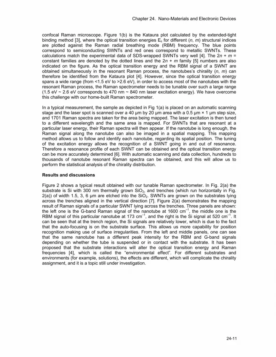
Figure 1: (online colour at: www.pss-b.com) Method for obtaining a chirality distribution of a SWNT material. (a) Schematic diagram of the sample used in these experiments. (b) Kataura plot calculated by the extended-tight binding method [3]
In these proceedings we present our methodology of characterizing the chirality distribution of SWNT materials with tunable Raman spectroscopy. Figure 1 explains the basic procedure. Figure 1(a) is a schematic diagram of the sample used in our method. The gray area is part of the substrate and the yellow squares are markers for position recognition. The dimensions of the markers are 0.5 ~ 1 μm and the distance between them is ~20 μm. The black lines indicate nanotubes which can be either directly grown on the substrate or dispersed from solutions of a bulk material. The samples are then put onto an automatic scanning stage of a home-built
Chapter 24. Nano-Materials and Electronic Devices
24-11
confocal Raman microscope. Figure 1(b) is the Kataura plot calculated by the extended-tight binding method [3], where the optical transition energies Eii for different (n, m) structural indices are plotted against the Raman radial breathing mode (RBM) frequency. The blue points correspond to semiconducting SWNTs and red ones correspond to metallic SWNTs. These calculations match the experimental data of SDS-wrapped SWNTs very well [4]. The 2n + m = constant families are denoted by the dotted lines and the 2n + m family [5] numbers are also indicated on the figure. As the optical transition energy and the RBM signal of a SWNT are obtained simultaneously in the resonant Raman process, the nanotubes’s chirality (n, m) can therefore be identified from the Kataura plot [4]. However, since the optical transition energy spans a wide range (from <1.5 eV to >2.6 eV), in order to access most of the nanotubes with the resonant Raman process, the Raman spectrometer needs to be tunable over such a large range (1.5 eV ~ 2.6 eV corresponds to 470 nm ~ 840 nm laser excitation energy). We have overcome this challenge with our home-built Raman spectrometer. In a typical measurement, the sample as depicted in Fig 1(a) is placed on an automatic scanning stage and the laser spot is scanned over a 40 μm by 20 μm area with a 0.5 μm × 1 μm step size, and 1701 Raman spectra are taken for the area being mapped. The laser excitation is then tuned to a different wavelength and the same area is mapped. For SWNTs that are resonant at a particular laser energy, their Raman spectra will then appear. If the nanotube is long enough, the Raman signal along the nanotube can also be imaged in a spatial mapping. This mapping method allows us to follow and identify each nanotube, regarding its spatial position. The tuning of the excitation energy allows the recognition of a SWNT going in and out of resonance. Therefore a resonance profile of each SWNT can be obtained and the optical transition energy can be more accurately determined [6]. With automatic scanning and data collection, hundreds to thousands of nanotube resonant Raman spectra can be obtained, and this will allow us to perform the statistical analysis of the chirality distribution. Results and discussions Figure 2 shows a typical result obtained with our tunable Raman spectrometer. In Fig. 2(a) the substrate is Si with 300 nm thermally grown SiO2, and trenches (which run horizontally in Fig. 2(a)) of width 1.5, 3, 6 μm are etched into the SiO2. SWNTs are grown on the substrates lying across the trenches aligned in the vertical direction [7]. Figure 2(a) demonstrates the mapping result of Raman signals of a particular SWNT lying across the trenches. Three panels are shown: the left one is the G-band Raman signal of the nanotube at 1600 cm–1, the middle one is the RBM signal of this particular nanotube at 173 cm–1, and the right is the Si signal at 520 cm–1. It can be seen that at the trench region, the Si signals are relatively lower, which is due to the fact that the auto-focusing is on the substrate surface. This allows us more capability for position recognition making use of surface irregularities. From the left and middle panels, one can see that the same nanotube has a different peak intensity for the RBM and G-band signals depending on whether the tube is suspended or in contact with the substrate. It has been proposed that the substrate interactions will alter the optical transition energy and Raman frequencies [4], which is called the “environmental effect”. For different substrates and environments (for example, solutions), the effects are different, which will complicate the chirality assignment, and it is a topic still under investigation.

Chapter 24. Nano-Materials and Electronic Devices
24-12 RLE Progress Report 149
Figure 2: (online colour at: www.pss-b.com) Typical results obtained with the tunable Raman spectrometer. (a) Spatial mapping capability allows the registering of each nanotube with regard to its position. The laser excitation wavelength is 579 nm in this example. (b) Resonant energy profile of a metallic nanotube.
In Fig. 2(b) we demonstrate the example of the resonant profile of a metallic nanotube, which is identified as a (10, 4) nanotube in the Katuara plot (it is circled in Fig. 1(b)). Due to the trigonal warping effect [8], the optical transition energy for non-armchair metallic nanotubes splits, as can be seen in the Kataura plot. When the RBM signal (240 cm–1) intensity versus the excitation energy is plotted, an interesting two-peak resonance can be seen in the resonant profile, confirming the theoretical prediction. The red dots are experimental data and the black curve shows the calculated resonance profiles for the RBM intensity for both transitions obtained from time-dependent third-order perturbation theory [9]. The blue diamonds indicate the predicted resonant energy. From our results we concluded that there is a downshift of ~70 meV for the resonant energy between the experimental data and theoretical prediction, which is due to the environmental effect mentioned above.
Figure 3 (online color at: www.pss-b.com) Preliminary results for the comparison of two samples grown at two different temperatures (the rest of the growth conditions are all the same). (a) Growth carried out at 650 °C. Green dots are the data points. (b) Growth at 900 °C. Yellow dots are the data points.

Chapter 24. Nano-Materials and Electronic Devices
24-13
With the spatial mapping and energy profile capabilities confirmed for our Raman spectrometer, we investigated two SWNT samples grown with the same catalyst and same chemical vapor deposition (CVD) conditions except for the growth temperature. The catalyst is Al2O3 supported Fe/Mo nanoparticles [10] directly spun onto Si/SiO2 substrates and the CVD conditions at the growth temperature are methane with a flow rate of 1000 standard cubic centimeter per minute (sccm) mixed with hydrogen of 500 sccm. The growth temperatures for the two samples are 650 °C and 900 °C respectively. In Fig. 3 the data of the samples are shown. The calculated Kataura plots are also displayed for reference. Figure 3(a) corresponds to the data obtained with the sample grown at 650 °C (green dots), and Fig. 3(b) displays the data of the sample grown at 900 °C (yellow dots). The blue shaded areas indicate the regions where we have laser excitation energies available. The size of the dots is proportional to the logarithm of the intensities of the Raman signal. Currently we are limited by the available laser sources, and thus are not able to perform the chirality distribution for these two samples. However, these preliminary results demonstrate the effectiveness of the basic principle. In addition, we can see that there is a fairly large environmental effect: the experimental data points appear at lower excitation energy and at a slightly higher RBM frequency compared with the calculated ones. Since these calculated results fit the SDS-wrapped nanotubes in water solutions fairly well, it is reasonable for the nanotube lying on Si to have a different environmental shift. However, this complicates the chirality assignment and renders the (n, m) identification not definitive when two (n, m) points are very close to each other. Further in-depth investigations of the environmental effect will be carried out in order to achieve clear chirality assignment in the future. Nevertheless, it can be seen from Fig. 3 that once the rest of the laser excitation energies are available, it will be straight forward to obtain a diameter distribution and metallic/semiconducting ratio characterization easily.
With these preliminary results, we performed a rough estimate of metallic to semiconducting nanotube ratio. For the 900 °C sample, we have observed 256 RBM signals within the current excitation ranges for 160 cm–1 ≤ ωRBM ≤ 340 cm–1 (we exclude ωRBM < 160 cm–1 because at blue excitation energies, small ωRBM are difficult to observe). Among these, 130 correspond to metallic SWNTs, 126 correspond to semiconducting ones. The same SWNT can be observed at different excitation energies if the laser energies are close enough to be within the nanotube’s resonance window. We include this factor into our consideration by using a ±0.1 eV resonance window and a 50 meV environmental downshift (these parameters work well for our experimental data points) and found that it is expected to observe 177 RBM signals corresponding to metallic nanotubes and 166 RBM signals corresponding to semiconducting nanotubes. This means if there is no preference in the chirality distribution, there should be a roughly 1:1 ratio of metallic to semiconducting nanotubes in these laser excitation regions. Our results give 130:126, which falls within this energy range. For the 650 °C sample, we observed 29 RBM signals corresponding to metallic SWNTs and 53 for semiconducting nanotubes in the region 160 cm–1 ≤ ωRBM ≤ 340 cm–
1. The number of data points at the current stage is not enough for making a statistically meaningful estimate for this sample. References
[1] M.S. Dresselhaus, G. Dresselhaus, and Ph. Avouris, Carbon Nanotubes: Synthesis, Structure, Properties and Applications (Springer Verlag, Berlin, 2001).
[2] C.L. Kane and E.J. Mele, Phys. Rev. Lett. 78: 1932 (1997). [3] G.G. Samsonidze, R. Saito, N. Kobayashi et al., Appl. Phys. Lett. 85: 5703 (2004) [4] C. Fantini, A. Jorio, M. Souza et al., Phys. Rev. Lett. 93: 147406 (2004) [5] S.M. Bachilo, M.S. Strano, C. Kittrell et al., Science 298: 2361 (2002) [6] A. Jorio, R. Saito, J.H. Hafner et al., Phys. Rev. Lett. 86: 1118 (2001) [7] Y.Y. Zhang, J. Zhang, H.B. Son, J. Kong, and Z.F. Liu, J. Am. Chem. Soc. 127: 17156
(2005) [8] R. Saito, G. Dresselhaus, and M.S. Dresselhaus, Phys. Rev. B 61: 2981 (2000)

Chapter 24. Nano-Materials and Electronic Devices
24-14 RLE Progress Report 149
[9] H.B. Son, A.R. Cecco, G.G. Samsonidze et al., “Raman characterization of electronic transition energies of metallic single-wall carbon nanotubes,” Physical Review B 74: 073406 (2006)
[10] J. Kong, H.T. Soh, A.M. Cassell, C.F. Quate, and H.J. Dai, Nature 395: 878 (1998)
4. CVD Synthesis of Single-Walled Carbon Nanotubes from Gold Nanoparticle Catalysts Sponsor Focus Center Research Program-IFC, NSF-CHE 0111370 and NIH-RR02594
Project Staff S. Bhaviripudi, E. Mile, S.A. Steiner III, A.T. Zare, M.S. Dresselhaus, A.M. Belcher and J. Kong
Single-walled carbon nanotubes (SWNTs) possess an appealing array of physical properties which give them great potential for a growing number of technological applications.1,2 Understanding how to control the synthesis of SWNTs is vital in order to deterministically integrate such nanostructures into various technologies. To date, the most versatile techniques for synthesizing SWNTs have been those based on catalyst-assisted chemical vapor deposition (CVD). In these techniques, metal-based nanoparticles serve as catalysts in both assisting carbon feedstock cracking and in facilitating the nucleation of nanotubes. In every variation of the CVD method used for synthesizing SWNTs, the composition and morphology of the catalyst nanoparticles are critical in determining the structure, length, and yield of nanotubes which will result. By far, the majority of work reporting CVD synthesis of carbon nanotubes has focused on nanoparticle catalysts based on Fe, Co, and Ni.
At the same time, there have been reports of SWNT and multi-walled nanotube growth employing catalysts based on other metals.3-5 Exploring alternative catalysts for nanotube growth is an interesting prospect for a number of reasons. For example, NMR experiments have indicated that the ratio of metallic to semiconducting SWNTs grown with Co/Ni-based catalysts is different than when Rh/Pd catalysts are used.6 This suggests that it may be possible to change the ratio of metallic to semiconducting nanotubes by varying the catalyst composition. In addition, at present in the field of nanotube research, there is not a clear understanding regarding the important factors for catalyzing nanotube growth. Based on the evaluation of carbon solubility and carbide stability from the carbon-metal binary phase diagrams, it has been suggested that Fe, Co and Ni are the only elements capable of catalyzing SWNT growth amongst 70 elements that include all of the transition metals.7 However, this is contradicted by experimental results. Therefore, a detailed comparison between the similarities and differences of various metal catalysts will help to elucidate the growth mechanism in greater depth.

Chapter 24. Nano-Materials and Electronic Devices
24-15
Figure 1: (a) TEM image showing monodisperse Au nanoparticles (b) High energy resolution XPS spectra of Au nanoparticles at different stages of treatment. (c) A typical AFM height image (5.0 × 3.9 µm2) and the corresponding cross sectional image. (d) SEM image of nanotubes grown from Au catalysts.
Gold is one potentially interesting alternative to Fe, Co, and Ni. Bulk gold has historically been regarded as relatively inactive towards catalyzing chemical reactions due to its completely filled 5d shell and relative high first ionization energy.8 Over the past decade, however, it has been shown that nanoscale gold particles possess enhanced catalytic activity over their bulk counterpart due to size effects.4,9 Additionally, bulk Au has a melting point of 1064°C, and so due to size effects, Au nanoparticles of diameters suitable for SWNT growth are expected to have melting points as low as 300°C.10 This low melting point may enable lower CVD growth temperatures than is possible with Fe, Co, and Ni under otherwise identical conditions, advantageous for the direct integration of nanotubes into different technologies with temperature-limiting materials and particals. Growth was carried out using highly monodisperse Au-nanoparticle catalysts prepared by block co-polymer templating technique.11 Synthesis of SWNTs and MWNTs from catalysts prepared using block copolymer templates has been recently reported during the past few years.12-14 In a typical experiment, 0.2 g polystyrene-poly(4-vinylpyridine) (PS-P4VP) di-block copolymer is dissolved in 50 ml toluene to form reverse micelles in toluene consisting of polar P4VP cores in non-polar PS domains.11 2 mg of tetrachloroauric acid (HAuCl4. 3H2O) is added to the solution. Interactions between the Au salt and pyridine unit of the PS-P4VP sequester Au ions within the spherical micellar domains. The Au-loaded polymer micellar solution is then spin-coated onto Si/SiO2 substrates to form a monolayer of micelles. Subsequently, O2 plasma treatment is carried out to remove the polymeric shell. Figure 1a is a transmission electron microscopy (TEM) image of the Au nanoparticles. The lattice fringes from a gold nanocrystal are seen in the inset. The syntheses of SWNTs were carried out in a 2.5-cm diameter quartz tube furnace. Typically, substrates with Au nanoparticles (after O2 plasma treatment) were loaded into the quartz tube and heated to growth temperature (800°C or 900°C) under Ar flow. At the growth temperature, the flow of Ar was replaced by a flow of 440 sccm H2 and maintained for 15 min to reduce the nanoparticles. Subsequently, the synthesis was initiated by introducing a flow of 20 sccm C2H4, 30 sccm CH4, and 440 sccm H2 for 10 min. After growth, the hydrocarbon gases were turned off, the tube removed from the furnace, and a flow of 600 sccm Ar activated as the tube cooled to room temperature. Numerous trials were performed to evaluate the influence of various process parameters on nanotube yield. It was found that no growth would occur without a reductive pretreatment, and that a process temperature of 800°C resulted in a higher yield than 900°C. Figure 1b shows the

Chapter 24. Nano-Materials and Electronic Devices
24-16 RLE Progress Report 149
high-resolution X-ray photoelectron (XPS) spectra of Au nanoparticles after O2 plasma, after reductive pretreatment, and finally after CVD. Two chemistries of gold are observed prior to the reductive pretreatment, with the higher binding energy possibly attributable to either a residual shell of gold chloride or gold oxide (as a result of plasma treatment) on the nanoparticles. These higher binding energy chemistries disappear after the reductive pretreatment, suggesting that the H2 treatment successfully removes this residual material. Given the inability of unreduced particles to successfully catalyze nanotube growth, it can be concluded that the presence of these higher binding energy chemistries of gold somehow inhibits nanotube growth. The presence of densely populated nanotubes on the surface of the substrate after CVD at 800ºC as shown in a representative scanning electron microscopy (SEM) image (Fig. 1d) indicates that Au serves as an efficient catalyst. Atomic force microscopy (AFM) height images of nanotubes reveal that the growth of nanotubes occurs from individual catalyst nanoparticles with diameters ranging from 1 to 2 nm (Fig. 1c). Resonant Raman spectra of nanotubes were collected using a laser excitation wavelength of 685 nm. The presence of radial breathing modes (RBM) in the spectra at various spots on the surface verifies that these structures are SWNTs (Fig. 2). Using the relationship for nanotube diameter dt (nm) = 233 cm-1/ωRBM,15 the diameters of the SWNTs are found to be between 1.2 to 1.8 nm, consistent with the AFM height measurements. In addition, the absence of disorder-induced Raman mode (D-band) at around 1300 cm-1 indicates the high quality of as-grown SWNTs (inset of Fig. 2).
Figure 2: Raman spectra of the nanotube sample grown with the Au catalyst. The inset shows the G-band and the absence of D-band.
Interestingly, a decrease in the density of the gold nanoparticles on the substrate is observed after CVD. This could be due to either evaporation of gold from the substrate (as a result of the low melting point of the Au nanoparticles) or possibly due to the diffusion of gold into the substrate. Further investigation will be carried out to understand this phenomenon. In addition, the average diameter of the nanoparticles (as measured by AFM) appears to decrease as (from 3.1 ± 0.4 nm to ~2.0 nm, see Supplementary Information). This could again be due to the evaporation of gold from the substrate or due to reduction of the oxide shell. At present, our attempts to grow SWNTs at temperatures lower than 800ºC using thermal CVD have not been successful. We believe this is mainly due to the thermal energy required for cracking the carbon feedstock. A two-stage furnace or other means to decompose the hydrocarbon gases, such as hot-filament CVD or plasma-enhanced CVD,16 may eventually lead to a lower growth temperature with Au nanoparticle catalysts. In summary, the growth of SWNTs using gold nanoparticle catalysts was successfully demonstrated. Investigations are currently underway to achieve low temperature SWNT growth. Furthermore, a detailed analysis with resonant Raman spectroscopy17 will be carried out to elucidate the metallic to semiconducting ratio of the SWNTs. Given the increased inter-atomic distance of Au over Fe, Co, or Ni, it is possible the chirality distribution of SWNTs grown from the Au nanoparticles could be different from those of conventional catalysts. Our successful synthesis opens up the route for the investigation of chirality modification through parameter control during the CVD.

Chapter 24. Nano-Materials and Electronic Devices
24-17
References
[1] S.J. Tans, A.R.M. Verschueren, C. Dekker Nature 393: 49-52 (1998) [2] M. Fuhrer, H. Park, P.L. McEuen, IEEE Trans. Nanotec. 1: 78-88 (2002) [3] C.J. Lee, S.C. Lyu, H.W. Kim, J.W. Park, H.M. Jung, J. Park, Chem. Phys. Lett. 361:
469-472 (2002) [4] S.Y. Lee M. Yamada, M. Miyake, Carbon 43: 2654-2663 (2005) [5] R.L.V. Wal, T.M. Ticich, V.E. Curtis, Carbon 39: 2277-2289 (2001) [6] X.P. Tang, A. Kleinhammes, H. Shimoda L. Fleming, K.Y. Bennoune, S. Sinha, C.
Bower, O. Zhou, Y. Wu Science 288: 492-494 (2000) [7] C.P. Deck, and K. Vecchio, Carbon 44: 267-275 (2006) [8] J.C. Bailar, Comprehensive Inorganic Chemistry, vol. 1, Pergamon, New York, 1973, p.
129 [9] G. Schmid, Chem. Rev. 92: 1709-1727 (1992) [10] P. Buffat, J.P. Borel, Physical Review A 13: 2287-2296 (1976) [11] (a) J.P. Spatz, S. Mossmer, C. Hartmann, M. Moller, Langmuir 16: 407-415 (2000)
(b) R. Glass, M. Moller and J.P. Spatz Nanotechnology 14: 1153-1160 (2003) [12] J. Lu, S.S. Yi, T. Kopley, C. Qian, J. Liu, E. Gulari J. of Phys. Chem. B 110: 6655-6660
(2006) [13] S. Bhaviripudi, A. Reina, J. Qi, J. Kong, A.M. Belcher, Nanotechnology 17: 5080-5086
(2006) [14] R.D. Bennett, A.J. Hart, R.J. Cohen, Adv. Mater. 18: 2274-2279 (2006) [15] J. Kurti, V. Zolyomi, M. Kertesz, G. Sun, New J. Phys. 5: 125.1-125.21 (2003) [16] Y. Li, D. Mann M. Rolandi, W. Kim, A. Ural, S. Hung, A. Javey, J. Cao, D. Wang, E.
Yenilmez, Q. Wang, J.F. Gibbons, Y. Nishi, H. Dai Nano. Lett. 4: 317-321 (2004) [17] H.B. Son, A. Reina, M.S. Dresselhaus, J. Kong Phys. Stat. Sol. B 243: 3161-3165 (2006)
5. Raman Spectra Variation of Partially Suspended Individual Single-Walled Carbon Nanotubes
Sponsor Intel Higher Education Program, NSF DMR 04-05538
Project Staff H. Son, M.S. Dresselhaus, J. Kong Collaboration with Y. Zhang, J. Zhang and Z. Liu at Peking University Introduction Resonance Raman spectroscopy has been demonstrated to provide a powerful tool for characterizing the structure of carbon nanotubes (CNTs). In particular, a strong Raman signal can be observed for an individual single-walled carbon nanotube (SWNT), when one of its electronic transition energies Eii is in resonance with the laser energy Elaser. By comparing the experimental resonant energy Eii and the radial breathing mode (RBM) frequency ωRBM with the theoretically calculated Kataura plot, it is possible to determine the diameter and the chiral indicies (n,m) of the SWNT.1

Chapter 24. Nano-Materials and Electronic Devices
24-18 RLE Progress Report 149
The Raman spectra of SWNTs have been shown to be sensitive to the nanotube’s environment,2-
4 including whether the tube is in a bundle or is an isolated SWNT, or whether it is in a solution or sitting on a substrate or freely suspended. For nanotube samples in solution, the wrapping agents and solvents represent different environments as well, since they can be polar or nonpolar. Since the ωRBM is of great importance for deducing the geometric structure of a SWNT by resonance Raman spectroscopy and Eii is an essential factor determining the electrical and optical properties of the SWNT, it is very important to understand and exploit these environmental effects.5-8 Theoretical calculations have predicted that tube-tube interactions within a bundle will cause a ~6-20 cm-1 upshift in RBM frequencies compared with isolated tubes due to the space restrictions imposed by the presence of neighboring tubes.9-11 It was also inferred from experiments that the resonant energy Eii of a SWNT in a bundle will be higher than when the nanotube is isolated.12 However, more recent studies show an unchanged ωRBM frequency but lower Eii for nanotubes in bundles compared with isolated tubes wrapped by sodium dodecyl sulfate (SDS) in aqueous solution.2 These previous investigations were all carried out with SWNT samples in bulk form, either as a solid or dispersed in solution. A direct investigation on specific individual SWNTs will be highly desirable to uncover and clarify further details regarding environmental effects. Such studies are lacking at present.
In our recent communication,13 ultralong individual SWNTs were successfully prepared on trench-containing substrates, which provide nanotubes with both suspended and nonsuspended segments. These samples serve as ideal systems for investigating environmental effects (in this case, substrate interactions) on individual SWNTs. In the present work, we report on the Raman signal variation (in terms of the intensity, frequency, line width, and intensity ratio between Stokes and anti-Stokes signals) by comparing the corresponding Raman features between the suspended and nonsuspended segments along the same SWNT. Our experiments are carried out with low enough laser excitation power so that the effect of laser heating on the suspended segments can be excluded. We collected RBM and G-mode Raman spectra for 15 individual SWNTs and compared the observed variations in detail, and the environment effects on the same nanotube have been systematically studied.
Experimental Section
Figure 1. (a) A schematic illustration of the trench-containing substrate (type A) with the catalyst being deposited at one edge of the substrate and used for the subsequent CVD preparation of SWNTs. (b) A schematic illustration of an individual SWNT suspended over trenches. (c) An SEM image showing oriented long SWNTs on a trench (300 nm deep)-containing substrate. (d) An SEM image of an individual SWNT crossing trenches (10 nm deep, 1 to 10 µm wide). (e) A zoomin SEM image at one edge of a trench (10 µm deep, 6 µm wide) showing that the nanotube is well suspended over the trench. (In the SEM image, the lighter color indicates the trench.)
A. SWNT Preparation and Characterization An illustration of the sample preparation is shown in Figure 1, parts a and b. The substrates used in this study are silicon pieces with a 300 nm thick SiO2 film. Photolithography and dry etching were used to pattern 1-80 µm wide trenches on the surface. Two types of substrates with trench depths of 300 nm (type A) and 10 µm (type B) were used in this study.

Chapter 24. Nano-Materials and Electronic Devices
24-19
SWNTs were grown by the catalytic chemical vapor decomposition (CVD) of ethanol.14 A 0.01 M FeCl3 ethanol solution was applied by microcontact printing to one edge of the substrate. The substrate was then placed in a horizontal 1.5 in. quartz furnace with the catalyst end directed toward the gas flow. The substrate was heated at 900 °C for 30 min in a flow of Ar/H2 (500 sccm/30 sccm) and then ethanol was introduced into the furnace by bubbling 200 sccm Ar through the ethanol. The growth was terminated after 30 min by switching the gas to Ar/H2 (500 sccm/30 sccm) and cooling the furnace.
As shown in Figure 1c, an SEM image of the prepared samples revealed that well-separated, millimeter to centimeter long carbon nanotubes with a controlled orientation can be routinely prepared on the trench-containing substrate. For the samples with 300 nm deep trenches, carbon nanotubes can be suspended over 3 µm wide trenches, while for the sample with 10 µm deep trenches, nanotubes are suspended over 10 µm wide trenches. For wider trenches, some SWNTs come into contact with the bottom of the trench. Parts d and e of Figure 1 show an individual SWNT that spans the trenches with 1 to 10 µm widths and is well suspended over them. This indicates that the nanotubes are floating above the substrate during the growth. TABLE 1: Summary of Data for 15 SWNTs that were investigated in this study, among which three SWNTs (Nos. 6, 13, and 14) are on a Type B Substrate (10 µm Deep Trench) and the Others are on a Type A (300 nm Deep Trench) Substratea
ωRBM (cm-1) fwhm (cm-1) IAS/IS RBM intensity
Number SUS ΔωRBM SUS SOS SUS SOS SU) (au) ISUS/ISOS
1 282.5 0 2.4 2.8 0.12 0.09 0.038 2.3
2 243.7 +1.3 5.6 3.8 1.23 0.88 0.0088 0.53
3 201.7 0 7.0 7.0 0.10 0.16 0.11 2.4
4 200.4 -0.1 3.6 4.8 0.13 0.14 0.0078 0.087
5 193.7 +0.6 4.4 5.3 0.14 0.16 1.0 18
6 187.4 +0.9 2.9 2.7 0.13 0.18 0.061 0.94
7 169.8 -0.3 2.8 2.8 0.40 0.27 0.39 4.1
8 167.6 0 3.1 3.3 0.80 0.80 0.0095 2.5
9 159.9 0 4.0 6.4 1.0 0.70 0.0050 1.1
10 157.5 -0.8 8.2 13 0.96 0.39 0.0067 2.2
11 148.4 -0.3 3.6 4.5 1.1 0.60 0.038 2.6
12 144.0 +0.6 4.1 4.0 0.82 0.84 0.0063 5.4
13 129.9 0 5.4 11 1.7 0.44 0.0073 3.2
14 117.0 0 4.9 4.0 0.7 1.20 0.017 14
15 115.8 -0.3 4.6 7.1 1.55 1.25 0.048 30
a Each row corresponds to data taken from the same SWNT. SUS indicates the data of a suspended segment and SOS means that from a segment sitting on a substrate. IAS/IS is the intensity ratio of the anti-Stokes to Stokes of the RBM features and fwhm (cm-1) is the full width at half-maximum of the RBM Raman peak. The units of the intensity are arbitrary and in this table we use the highest intensity as a normalization factor. ISUS/ISOS is the intensity ratio of the SUS segment to the SOS segment of the same SWNT

Chapter 24. Nano-Materials and Electronic Devices
24-20 RLE Progress Report 149
B. Raman Spectra Measurements Resonant Raman spectroscopy (Renishaw microprobe RM1000) with a 632.8 nm (1.96 eV) He-Ne laser was used in this study. The excitation spot size is about 1 µm2, using a 50_ objective lens. The excitation laser power ranges from 0.04 to 1.07 mW at the sample. With the help of the SEM image and using the trench structures on the substrate as markers, a micro-Raman spectroscopy study on an individual nanotube can be readily carried out. Generally, we first scan the laser spot along a trench (which is perpendicular to the SWNTs) to find resonant nanotubes. We next locate the precise position of a particular SWNT by looking for the strongest signal to make sure that the laser spot is right on top of the nanotube, and then we collect Raman spectra at that location. All spectra are taken with the light polarized parallel along the nanotube axis. Raman spectra of the 15 SWNTs (12 are on the type A substrate and 3 are on the type B substrate, see Table 1) are obtained from both the suspended (SUS) segments and the sitting-on-substrate (SOS) segments. The signals of the suspended segment of the 12 nanotubes on the type A substrate are taken over the 3 µm wide trenches, those of the No. 6 and No. 13 nanotubes are taken from the 6 µm wide trenches, those of the No. 14 nanotubes are taken from a 4 µm wide trench. In fact, our intention of using the type B substrate (deeper trenches, and nanotubes can be suspended over wider trenches) is to check whether the signals of the suspended segment of the same nanotube are the same over trenches with different widths. As observed experimentally, the Raman behaviors of suspended SWNTs are the same as long as the distance between the laser spot and the trench edge is above 1.5 µm (including 1.5 µm). So, as the signals for the suspended segments of these 15 SWNTs are all taken from trenches with width ≥ 3 µm (2 x 1.5 µm), it is reasonable to put them together for comparison. We focus on the RBM and G-band features in this study. The RBM peak positions (ωRBM), intensity, and full width at half-maximum (fwhm) are all obtained by fitting the spectra with use of a Lorentzian line shape. These values as well as the change in RBM frequency (ΔωRBM) and the anti- Stokes to Stokes RBM intensity ratios (IAS/IS) between the two segments are summarized in Table 1.
Note that, although the resolution of the spectrometer is about ~1 cm-1, the peak position stability in our experiments is much better than 1 cm-1 as observed experimentally, and therefore we believe that the peak shifts below 1 cm-1, when comparing suspended and nonsuspended segments, are due to environmental effects.
Results and Discussion
To clarify any possible laser heating effect, we first collect Raman spectra for each SWNT at every point and compare its spectra using various laser power levels. For the SOS parts of almost all the nanotubes, there was no observable heating effect when using a laser power of ≤ 1.07 mW, which is consistent with what has been previously reported15-17 and can be ascribed to the underlying substrate (SiO2) as an effective heat sink.18 However, for the SUS segments, the Raman spectra of most SWNTs show variations in RBM peak frequency, fwhm, and IAS/IS when changing the laser power from lower power levels to 1.07 mW (the highest power level in our setup), which indicates a heating effect for suspended SWNTs with a laser power of 1.07 mW. This can be explained by the poor thermal dissipation of the suspended SWNT to its surroundings due to its nanometer-scale cross section.19,20 So to investigate the intrinsic Raman spectral variation for each SWNT, we first collect Raman spectra with different laser power levels for its SUS and SOS segments separately and make sure that the spectra we used for the discussion of the environmental effect below are free of laser heating.

Chapter 24. Nano-Materials and Electronic Devices
24-21
Figure 2. Raman spectra from a suspended segment (upper line) and from a segment sitting on substrate (lower line) of an individual SWNT. All the spectra are collected with a laser power of 0.13 mW and the integration time is 30 s. The G mode intensity is multiplied by 10 (suspended) and by 50 (sitting on substrate) to display the spectra clearly in the same panel of the figure.
Figure 2 shows Raman spectra obtained from the SUS and SOS segments of the same SWNT demonstrating the striking contrast between the spectra from the two segments. From our observations, the spectra from the SUS and SOS segments of the same SWNT may exhibit differences in intensity, frequency, fwhm, and IAS/IS for the RBM, and also differences in intensity, frequency, line shape, and fwhm for the various features of the G-band.
First of all, suspended SWNTs usually show enhanced Raman signals, which can be seen in Figure 2 as an example. This intensity-enhancement has been reported17 previously and was attributed to an undisturbed environment for the suspended SWNTs. The enhanced signals are quite beneficial for both studying Raman features that are normally weak (such as the Raman peak at ~1730 cm-1 in Figure 2) and enabling observation of SWNTs with a relatively poor resonance condition. In fact, for more than one-third of the SWNTs showing RBM Raman signals for the SUS segments, the corresponding SOS segments display no signals. According to our observations, the RBM intensity ratio of the Stokes signal obtained from the SUS segments to that obtained from the SOS segments (ISUS/ISOS) varies from one nanotube to another and a ratio of over 20 has been observed for particular tubes (see Table 1). Although most of the SWNTs show enhanced signals from their SUS segments compared with their SOS segments, there are also a few exceptions. Among the 15 SWNTs, there are two nanotubes (Nos. 6 and 9) with an RBM intensity ratio close to 1 and two other nanotubes (Nos. 2 and 4) with an RBM intensity ratio less than 1.
Although the SUS segments are expected to have anintrinsically higher Raman cross section21 than the SOS segment, the electronic transition energies are also expected to change for the SUS segments relative to the SOS segments,8,22 which can explain the smaller RBM intensity in the SUS segments as compared to the SOS segments in terms of the change in the resonance condition.
Figure 3. RBM frequency variation of an individual SWNT (No. 6) with the laser spot moving along the tube (0.5 µm per step) from the left side to the right side of a 6 µm wide trench. The laser power level used here is 0.31 mW. A schematic illustration of the trench containing substrate is included on the bottom to show the laser spot location.
The RBM frequencies (ωRBM) from the SUS and SOS segments of the same SWNT exhibit a small but observable shift in a few SWNTs. For an example, SWNT No. 6 shows an 0.9 cm-1 shift in the RBM frequencies. To see the spatial variation of ωRBM and to ensure the repeatability of ωRBM measurements, we have collected a series of spectra by moving the laser spot along the SWNT No. 6 from one side to the other side of the trench (6 µm wide, 10 µm deep) at 0.5 µm steps, and we have plotted its ωRBM versus laser spot locations (see Figure 3). A clear difference in ωRBM between the SUS and SOS segments is seen in Figure 3. Since the heating effect has been excluded, the difference must be due to the environmental variations along the nanotube. A

Chapter 24. Nano-Materials and Electronic Devices
24-22 RLE Progress Report 149
possible explanation is the van der Waals interaction between the substrate and the SWNT. A previous work9 has reported an ωRBM shift for SWNT bundles under different pressures and has attributed this shift to the intertube van der Waals interactions.
The fwhms of the RBM are reduced significantly in the SUS segments compared with the SOS segments for about half of the SWNTs listed in Table 1, while a few SWNTs actually exhibit larger fwhm values in the SUS segments. We expect that the perturbation-free environment for the SUS segments will give rise to smaller fwhm in the SUS segments in general.17 However, the change in the Eii can affect the resonance condition |Elaser - Eii| and might increase the fwhm values in the SUS segments.23
The observed IAS/IS changes can be explained by the changes in Eii values and the inverse lifetime of the intermediate electronic state. IAS/IS is given by the following:2
( )( )( )( )
2
laser laser ph phAS2
S Blaser laser ph
(exp.)= expii ii
ii ii
E E i E E E i EII k TE E i E E E i
⎡ ⎤− − Γ + − − Γ ⎛ ⎞⎣ ⎦ −⎜ ⎟⎡ ⎤ ⎝ ⎠− − Γ − − − Γ⎣ ⎦
(1)
where Elaser and Eii have the same meaning as formerly defined, Eph is the phonon energy (ωRBM), Γ is the inverse lifetime of the intermediate electronic state, kB is the Boltzmann constant, and T is the temperature of the SWNT. As the laser heating is excluded, the IAS/IS variation between the SUS and SOS segments of a SWNT must come from either Eii or Γ variations. Although our instrument does not have the capability to measure Eii and Γ values, our results indicate that there is significant Eii variation, at least for a few SWNTs. For example, the No. 10 nanotube has a thermal factor of exp(-Eph/kBT) ) 0.47 at room temperature (T ) 298 K), and its IAS/IS values are 0.96 and 0.39 for the SUS and SOS segments, respectively. This indicates that Eii > Elaser for the SUS segment and Eii < Elaser for the SOS segment for this nanotube. With a similar argument, we can conclude that the Eii of nanotube No. 13 also downshifts in the SOS segment, whereas it is highly possible that the Eii of nanotube No. 14 upshifts in the SOS segment. If Eii of nanotube No. 14 did not shift at all, or if it downshifted, the Γ value must be significantly smaller in the SOS segment than in the SUS segment, which contradicts the assumption that the SUS segment is free of environmental perturbation and should have a longer lifetime of the intermediate electronic state.
There are several possible explanations for the Eii variations. The first one is the charge transfer between the substrate and the SWNT. However, this is not very likely in our samples since the SiO2 is an insulating material. Another possible explanation is the different dielectric environment giving rise to the difference in the electron-electron Coulomb repulsion and the exciton binding energies.24,25 This is also excluded since this effect is weakly sensitive to the SWNT chirality26 and would shift the Eii in the same direction for all the SWNTs, which is not consistent with our experimental results. The last explanation is in terms of the van der Waals interaction between the substrate and the SWNT. Theoretical calculations showed that for nanotubes on a flat metal surface, the binding energy between the substrate and the SWNT will introduce a radial deformation and alter its electronic properties.27,28 It is also expected that the van der Waals interactions between a SWNT and a silicon substrate distort the cross section of nanotubes and that the distorted tube cross-section leads to a change in its electronic properties.6
The radial deformation induced by the nanotube-substrate interaction will most likely result in strain in the radial direction in the nanotube. And on the other hand, the Eii of semiconducting nanotubes was reported to shift in two directions depending on their (2n+m) mod 3 ) 1 or 2 family type.5,29,30 We make tentative (n,m) assignments for these three nanotubes using a previously reported method.3,13 Nanotube No. 13 can be assigned to one of following nanotubess(24,1)/(18,10)/(19,8)/(23,3)s which all fall into an (2n+m) mod 3 ) 1 family (type I), and the laser excitation energy used in this experiment corresponds to an E44 transition for this nanotube. Nanotube No. 14 is one of (25,3)/(23,7)/(20,10), which all fall into the (2n+m) mod 3 ) 2 family (type II), and the observed optical transition corresponds to an E44 transition. Similarly,

Chapter 24. Nano-Materials and Electronic Devices
24-23
tube No. 10 belongs to the (2n+m) mod 3 ) 2 family (type II) and the optical transition corresponds to an E33 transition. The analysis given above showed that the Eii of nanotubes No. 10 and No. 13 downshifts and the Eii of nanotube No. 14 upshifts in SOS segments compared to SUS segments. This is consistent with the predicted family behavior of Eii shifting for SWNTs under strain. Note that for nanotubes with the same type, its E33 and E44 should shift in reverse direction under strain.
The G-band of semiconducting SWNTs show little change except for a couple of SWNTs that exhibit a small shift of about 5 cm-1 in the G--mode frequency (see Figure 4b). The SWNT in Figure 4b did not show an RBM signal in the SOS segment and therefore is not included in Table 1. The G--mode frequency is related to the curvature of the SWNT wall.31 This is consistent with a possible radial deformation due to the van der Waals interaction between the substrate and the SWNT, although it still remains unclear why the RBM frequency variation often does not coincide with the G--mode frequency variation.
Figure 4. G-mode Raman spectra of two individual SWNTs (a and b) taken from suspended segments and from segments sitting on substrate. The laser power level, the integration time, and the corresponding peak positions (in cm-1) are shown in the inset. The peak positions in part a cannot be determined well due to its omplicated line shape.
On the other hand, the G-band of a few metallic SWNTs shows a striking difference between the SUS and SOS segments (see Figures 4a). First of all, the relative intensity between the higher frequency peak and the lower frequency Breit-Wigner- Fano (BWF) peak changes dramatically. Second, the frequency of the BWF peak or higher frequency peak often shifts, although the shift directions vary for different SWNTs. We believe that these changes are due to the electronic band structure modulation since the metallic G-band shape and frequency are closely related to the electron-phonon interaction and by changing the electronic band structure the strength of this interaction would change.31-37 Unfortunately, at present there is no single theoretical model that can explain every detail of the observations we have made on these samples. Conclusions We prepared partially suspended individual long SWNTs on trench-contained substrates and carried out a systematic investigation of the difference between SUS and SOS segments of 15 individual SWNTs. With the heating effect being excluded by using low laser power, spectral differences between the SUS and SOS segments of the same nanotube are recorded and analyzed. Most of the SWNTs under investigation show enhanced Raman signals at their SUS segment compared with the SOS ones, with the exceptions that two of the tubes exhibit a similar Raman intensity at the SUS and SOS locations and two tubes show a reverse result. Along with the distinct intensity contrast, moderate RBM frequency variations are observed for some nanotubes, and these variations can be attributed to nanotube-substrate interaction. By analyzing the behaviors of the fwhm and IAS/IS of RBM, we find out that the Eii of SWNTs shift when comparing the two different types of segments. Considering all possible reasons for the Eii variation, we believe that for our system the main reason is van der Waals interactions between the SWNT and the substrate, which may deform the SWNT sitting on the substrate in the radial direction and thereby modify its electronic DOS, while suspended nanotubes still retain their pristine properties. Although the very detailed mechanisms behind these spectral differences are not very clear yet, our work provides evidence for the local property tuning of individual SWNTs

Chapter 24. Nano-Materials and Electronic Devices
24-24 RLE Progress Report 149
by environmental effects. The approach taken in the present study can be readily extended to other 1D materials and can lead to a facile way to generate and manipulate diverse properties of a single 1D object. References
[1] M.S. Dresselhaus, G. Dresselhaus, R. Saito, A. Jorio. Phys. Rep. 409: 47 (2005) [2] C. Fantini, A. Jorio, M. Souza, M.S. Strano, M.S. Dresselhaus, M.A. Pimenta. Phys. ReV.
Lett. 93: 147406 (2004) [3] A. Jorio, R. Saito, J.H. Hafner, C.M. Lieber, M. Hunter, T. McClure, G. Dresselhaus, M.S.
Dresselhaus. Phys. Rev. Lett. 86: 1118 (2001) [4] L.M. Ericson, P.E. Pehrsson. J. Phys. Chem. B 109:20276 (2005) [5] L. Yang, J. Han. Phys. Rev. Lett. 85: 154 (2000) [6] T. Hertel, R.E. Walkup, P. Avouris. Phys. Rev. B 58: 13870 (1998) [7] A. Maiti. Nat. Mater. 2:440 (2003) [8] A.G. Petrov, S.V. Rotkin. Nano Lett. 3: 701 (2003) [9] U.D. Venkateswaran, A.M. Rao, E. Richter, M. Menon, A. Rinzler, R.E. Smalley, P.C.
Eklund. Phys. Rev. B. 59: 10928 (1999) [10] L. Alvarez, A. Righi, T. Guillard, S. Rols, E. Anglaret, D. Laplaze, J.L. Sauvajol. Chem.
Phys. Lett. 316: 186 (2000) [11] L. Henrard, E. Hernandez, P. Bernier, A. Rubio. Phys. Rev. B 60: R8521 (1999) [12] A.M. Rao, J. Chen, E. Richter U. Schlecht, P.C. Eklund, R.C. Haddon, D.U.
Venkateswaran, Y.K. Kwon, D. Tomanek. Phys. Rev. Lett. 86: 3895 (2001) [13] Y.Y. Zhang, J. Zhang, H.B. Son, J. Kong; Z.F. Liu. J. Am. Chem. Soc. 127: 17156 (2005) [14] L.X. Zheng, M.J. O’Connell, S.K. Doorn, X.Z. Liao, Y.H. Zhao, E.A. Akhadov, M.A.
Hoffbauer, B.J. Roop, Q.X. Jia, R.C. Dye, D.E. Peterson, S.M. Huang, J. Liu, Y.T. Zhu. Nat. Mater. 3: 673 (2004)
[15] Dresselhaus, M. S.; Dresselhaus, G.; Jorio, A.; Souza, A. G.; Saito, R. Carbon 40,: 2043 (2002)
[16] A.G. Souza, S.G. Chou, G.G. Samsonidze, G. Dresselhaus, M.S. Dresselhaus, L. An,, J. Liu, A.K. Swan, M.S. Unlu, B.B. Goldberg, A. Jorio, A. Gruneis, R. Saito Phys. Rev. B 69: 115428 (2004)
[17] H.B. Son, Y. Hori, S.G. Chou, D. Nezich, G.G. Samsonidze, G. Dresselhaus, M.S. Dresselhaus, E.B. Barros. Appl. Phys. Lett. 85: 4744 (2004)
[18] E. Pop, D. Mann, J. Cao, Q. Wang, K. Goodson, H.J. Dai. Phys. ReV. Lett. 95: 155505 (2005)
[19] M.E. Itkis, F. Borondics, A.P Yu, R.C. Haddon. Science 312: 413 (2006) [20] H. Cao, Q. Wang, D.W. Wang, H.J. Dai, Small 1: 138 (2005) [21] P. Corio, P.S. Santos, M.A. Pimenta, M.S. Dresselhaus. Chem Phys. Lett. 360: 557
(2002) [22] A. Maiti, A. Ricca. Chem. Phys. Lett. 395: 7 (2004) [23] S. Reich, C. Thomsen, P. Ordejon Phys. ReV. B 65: 155411 (2002) [24] T. Ando. J. Phys. Soc. Jpn. 66: 1066 (1997) [25] V. Perebeinos, J. Tersoff, P. Avouris. Phys. ReV. Lett. 92: 257402 (2004)

Chapter 24. Nano-Materials and Electronic Devices
24-25
[26] G.G. Samsonidze, R. Saito, N. Kobayashi, A. Gruneis, J. Jiang, A. Jorio, S.G. Chou, G. Dresselhaus, M.S. Dresselhaus. Appl. Phys. Lett. 85: 5703 (2004)
[27] S. Dag, O. Gulseren, S. Ciraci, T. Yildirim. Appl. Phys. Lett. 83: 3180 (2003) [28] N. Park, S. Hong. Phys. ReV. B 72: 045408 (2005) [29] D. Karaiskaj, C. Engtrakul, T. McDonald, M.J. Heben, A. Mascarenhas. Phys. ReV. Lett.
96: 106805 (2006) [30] A.G. Souza, N. Kobayashi, J. Jiang, A. Gruneis, R. Saito, S.B. Cronin, J. Mendes, G.G.
Samsonidze, G. Dresselhaus, M.S. Dresselhaus. Phys. ReV. Lett. 95: 217403 (2005) [31] A. Jorio, M.A. Pimenta, A.G. Souza, R. Saito, G. Dresselhaus, M.S. Dresselhaus. New J.
Phys. 5: 139 (2003) [32] V.N. Popov, P. Lambin. Phys. Rev. B 73: 085407 (2006) [33] M. Lazzeri, S. Piscanec, F. Mauri, A.C. Ferrari, J. Robertson. Phys. Rev. B 73: 155426
(2006) [34] S.M. Bose, S. Gayen, S.N. Behera. Phys. Rev. B 72: 153402 (2005) [35] C.Y. Jiang, K. Kempa, J.L. Zhao, U. Schlecht, U. Kolb, T. Basche, M. Burghard, A.
Mews. Phys. Rev. B 66: 161404 (2002) [36] S.D.M. Brown, A. Jorio, P. Corio, M.S. Dresselhaus, G. Dresselhaus, R. Saito, K.
Kneipp. Phys. Rev. B 6315: 155414 (2001) [37] M. Shim, T. Ozel, A. Gaur, C.J. Wang. J. Am. Chem. Soc 128: 7522 (2006)
Publications Journal Articles Bhaviripudi, S., E. Mile, et al. (2007). "CVD synthesis of single-walled carbon nanotubes from
gold nanoparticle catalysts." Journal of the American Chemical Society 129(6): 1516-1517.
Chou, S. G., H. Son, et al. (2007). "Length characterization of DNA-wrapped carbon nanotubes using Raman spectroscopy." Applied Physics Letters 90(13): 131109.
Duan, X. J., H. B. Son, et al. (2007). "Resonant raman spectroscopy of individual strained single-wall carbon nanotubes." Nano Letters 7(7): 2116-2121.
Farhat, H., H. Son, et al. (2007). "Phonon softening in individual metallic carbon nanotubes due to the Kohn anomaly." Physics Review Letters 99: 145506.
Gao, B., X. J. Duan, et al. (2007). "Raman spectral probing of electronic transition energy E-ii variation of individual SWNTs under torsional strain." Nano Letters 7(3): 750-753.
Reina, A., M. Hofmann, et al. (2007). "Growth mechanism of long and horizontally aligned carbon nanotubes by chemical vapor deposition." Journal of Physical Chemistry C 111(20): 7292-7297.
Son, H., G. G. Samsonidze, et al. (2007). "Strain and friction induced by van der Waals interaction in individual single walled carbon nanotubes." Applied Physics Letters 90(25): 253113.
Steiner, S. A., T. F. Baumann, et al. (2007). "Iron-doped carbon aerogels: Novel porous substrates for direct growth of carbon nanotubes." Langmuir 23(9): 5161-5166.
Zhang, Y. Y., H. Son, et al. (2007). "Raman spectra variation of partially suspended individual single-walled carbon nanotubes." Journal of Physical Chemistry C 111(5): 1983-1987.
Zhang, Y. Y., H. Son, et al. (2007). "Laser-heating effect on Raman spectra of individual suspended single-walled carbon nanotubes." Journal of Physical Chemistry C 111(5): 1988-1992.

Chapter 24. Nano-Materials and Electronic Devices
24-26 RLE Progress Report 149
Conference Papers Cho, T. S. L., K. J.;Kong, J.; Chandrakasan, A. P. (2007). “A Low Power Carbon Nanotube
Chemical Sensor System”. IEEE Custom Integrated Circuits Conference, San Jose, California.


