Embed Size (px)
Citation preview
Citation: Lin, B.-R. Analysis and
Implementation of a Bidirectional
Converter with Soft Switching
Operation. Processes 2022, 10, 561.
https://doi.org/10.3390/pr10030561
Academic Editor: Yu-En Wu
Received: 24 February 2022
Accepted: 10 March 2022
Published: 13 March 2022
Publisher’s Note: MDPI stays neutral
with regard to jurisdictional claims in
published maps and institutional affil-
iations.
Copyright: © 2022 by the author.
Licensee MDPI, Basel, Switzerland.
This article is an open access article
distributed under the terms and
conditions of the Creative Commons
Attribution (CC BY) license (https://
creativecommons.org/licenses/by/
4.0/).
processes
Article
Analysis and Implementation of a Bidirectional Converter withSoft Switching OperationBor-Ren Lin
Department of Electrical Engineering, NYUST, Yunlin 640, Taiwan; [email protected]
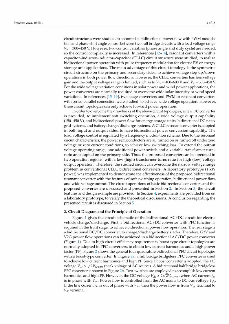
Abstract: This paper presents a soft switching direct current (DC) converter, with the benefitsof bidirectional power conversion and wide-ranging voltage operation for battery charging anddischarging capability. A series resonant circuit with variable switching frequency modulation is usedto achieve the advantages of soft switching turn-on or turn-off of semiconductor devices. Therefore,the switching power losses in power devices can be reduced. A symmetric resonant circuit topologywith a capacitor–inductor–inductor–capacitor (CLLC) structure is adopted to achieve a bidirectionalpower conversion capability for battery storage units in electric vehicle applications. Due to thesymmetric circuit structure on both input and output sides, the converter has similar voltage gainsfor each power flow operation. In order to overcome the drawback of narrow voltage range operationin conventional resonant converters, a variable transformer turns ratio is adopted in the circuit, toachieve wide output voltage operation (150–450 V) for battery charging applications. To demonstratethe converter performance, a 1-kW laboratory prototype was constructed and tested. Experimentalresults are provided, to verify the effectiveness of the studied circuit.
Keywords: series resonant converter; bidirectional DC converter; wide voltage gain; frequencymodulation
1. Introduction
Power converters with bidirectional power flow have been widely utilized betweenAC and DC grid systems and battery storage systems. Three-phase AC/DC bidirectionalpower factor correctors (PFC) [1,2] and DC/DC bidirectional converters [3–5] are adopted torealize forward and reverse power flow operations between AC grid and DC grid systems.The same circuit structures can be used for electric vehicle (EV) systems, to achieve vehicle-to-grid (V2G) and grid-to-vehicle (G2V) operations. The main advantages of AC/DC PFCare high power factor and low current harmonics. The bidirectional DC/DC converters canrealize forward/reverse power operations between the different DC voltage buses, such asbattery storage systems or EV battery units [6]. For renewable energy applications [7,8],wide voltage DC/DC and AC/DC converters are required in solar power and wind powerconversion, respectively, due to unstable solar intensity and wind speed. The basic circuittopologies of a bidirectional AC/DC converter are based on four or six three-leg activeswitches. These AC/DC converters can be controlled in PFC operation under forwardpower flow, or inverter operation under reverse power flow. The buck/boost DC/DCconverter is the basic topology for accomplishing bidirectional power conversion. Buck(boost) operation is controlled under forward (reverse) power flow. However, a buck/boostconverter has no electric isolation.
In [9], a pulse-width modulation converter was presented, to realize a bidirectionalpower flow capability with voltage step-down/step-up features during forward/backwardpower flow. However, a PWM converter cannot achieve both voltage step up/down de-mands under both power flow directions. The same drawback can be found in bidirectionalinductor–inductor–capacitor (LLC) resonant converters with synchronous switches on thesecondary side. In references [10,11], symmetric PWM converters with two full bridge
Processes 2022, 10, 561. https://doi.org/10.3390/pr10030561 https://www.mdpi.com/journal/processes
Processes 2022, 10, 561 2 of 18
circuit structures were studied, to accomplish bidirectional power flow with PWM modula-tion and phase-shift angle control between two full bridge circuits with a load voltage rangeVo = 300–450 V. However, two control variables (phase angle and duty cycle) are needed,so the control complexity is increased. In references [12–14], resonant converters with acapacitor–inductor–inductor–capacitor (CLLC) circuit structure were studied, to realizebidirectional power operation with pulse frequency modulation for electric EV or energystorage unit applications. The main advantage of this circuit topology is the symmetriccircuit structure on the primary and secondary sides, to achieve voltage step up/downoperations in both power flow directions. However, the CLLC converters has less voltagegain and the output voltage range is limited, such as to Vin = 400–600 V and Vo = 300–450 V.For the wide voltage variation conditions in solar power and wind power applications, thepower converters are normally required to overcome wide solar intensity or wind speedvariations. In references [15–19], two-stage converters and PWM or resonant converterswith series-parallel connection were studied, to achieve wide voltage operation. However,these circuit topologies can only achieve forward power operation.
In order to overcome the drawbacks of the above circuit topologies, a new DC converteris provided, to implement soft switching operation, a wide voltage output capability(150~450 V), and bidirectional power flow for energy storage units, bidirectional DC nano-grid systems, and battery charge/discharge systems. A CLLC resonant converter is adoptedin both input and output sides, to have bidirectional power conversion capability. Theload voltage control is regulated by a frequency modulation scheme. Due to the resonantcircuit characteristics, the power semiconductors are all turned on or turned off under zerovoltage or zero current conditions, to achieve low switching loss. To extend the outputvoltage operating range, one additional power switch and a variable transformer turnsratio are adopted on the primary side. Thus, the proposed converter can be operated intwo operation regions, with a low (high) transformer turns ratio for high (low) voltageoutput operation. Therefore, the studied circuit can overcome the narrow voltage rangeproblem in conventional CLLC bidirectional converters. A laboratory prototype (1 kWpower) was implemented to demonstrate the effectiveness of the proposed bidirectionalresonant converter with the features of soft switching operation, bidirectional power flow,and wide voltage output. The circuit operations of basic bidirectional converters and theproposed converter are discussed and presented in Section 2. In Section 3, the circuitfeatures and design example are provided. In Section 4, experiments are provided from ona laboratory prototype, to verify the theoretical discussions. A conclusion regarding thepresented circuit is discussed in Section 5.
2. Circuit Diagram and the Principle of Operation
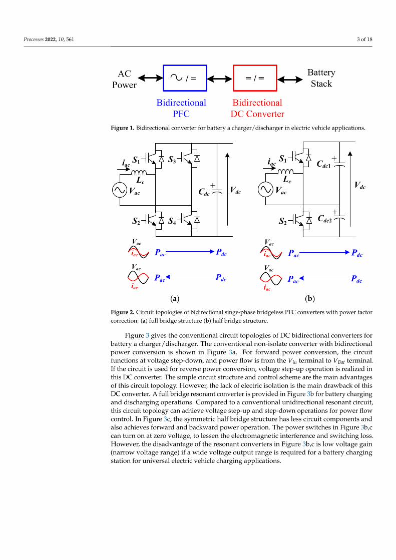
Figure 1 gives the circuit schematic of the bidirectional AC/DC circuit for electricvehicle charge/discharge. First, a bidirectional AC/DC converter with PFC function isrequired in the front stage, to achieve bidirectional power flow operation. The rear stage isa bidirectional DC/DC converter, to charge/discharge battery stacks. Therefore, G2V andV2G power flow operations can be achieved in a bidirectional AC/DC power converter(Figure 1). Due to high circuit-efficiency requirements, boost-type circuit topologies arenormally adopted in PFC converters, to obtain low current harmonics and a high powerfactor (PF). Figure 2 shows the general four quadrature bidirectional PFC circuit topologieswith a boost-type converter. In Figure 2a, a full bridge bridgeless PFC converter is usedto achieve low current harmonics and high PF. Since a boost converter is adopted, the DCvoltage Vdc >
√2Vac,rms (peak voltage of AC source). A bidirectional half bridge bridgeless
PFC converter is shown in Figure 2b. Two switches are employed to accomplish low currentharmonics and high PF. However, the DC voltage Vdc > 2
√2Vac,rms, when AC current iac
is in phase with Vac. Power flow is controlled from the AC mains to DC bus voltage Vdc.If the line current iac is out of phase with Vac, then the power flow is from Vdc terminal toVac terminal.
Processes 2022, 10, 561 3 of 18
Processes 2022, 10, x FOR PEER REVIEW 3 of 19
voltage Vdc. If the line current iac is out of phase with Vac, then the power flow is from Vdc terminal to Vac terminal.
/ =ACPower
= / = Battery Stack
BidirectionalPFC
BidirectionalDC Converter
Figure 1. Bidirectional converter for battery a charger/discharger in electric vehicle applications.
Vac
Lc
S1
S2
S3
S4
Cdc+
Pac
Vdc
Pdc
Vac
iac
Pac Pdc
Vac
iac
iac
VacVdc
Lc
S1
S2
Cdc1
Cdc2
+
+
Pac Pdc
Vac
iac
Pac Pdc
Vac
iac
iac
(a) (b)
Figure 2. Circuit topologies of bidirectional singe-phase bridgeless PFC converters with power fac-tor correction: (a) full bridge structure (b) half bridge structure.
Figure 3 gives the conventional circuit topologies of DC bidirectional converters for battery a charger/discharger. The conventional non-isolate converter with bidirectional power conversion is shown in Figure 3a. For forward power conversion, the circuit func-tions at voltage step-down, and power flow is from the Vin terminal to VBat terminal. If the circuit is used for reverse power conversion, voltage step-up operation is realized in this DC converter. The simple circuit structure and control scheme are the main advantages of this circuit topology. However, the lack of electric isolation is the main drawback of this DC converter. A full bridge resonant converter is provided in Figure 3b for battery charg-ing and discharging operations. Compared to a conventional unidirectional resonant cir-cuit, this circuit topology can achieve voltage step-up and step-down operations for power flow control. In Figure 3c, the symmetric half bridge structure has less circuit com-ponents and also achieves forward and backward power operation. The power switches in Figure 3b,c can turn on at zero voltage, to lessen the electromagnetic interference and switching loss. However, the disadvantage of the resonant converters in Figure 3b,c is low voltage gain (narrow voltage range) if a wide voltage output range is required for a battery charging station for universal electric vehicle charging applications.
Figure 1. Bidirectional converter for battery a charger/discharger in electric vehicle applications.
Processes 2022, 10, x FOR PEER REVIEW 3 of 19
voltage Vdc. If the line current iac is out of phase with Vac, then the power flow is from Vdc terminal to Vac terminal.
/ =ACPower
= / = Battery Stack
BidirectionalPFC
BidirectionalDC Converter
Figure 1. Bidirectional converter for battery a charger/discharger in electric vehicle applications.
Vac
Lc
S1
S2
S3
S4
Cdc+
Pac
Vdc
Pdc
Vac
iac
Pac Pdc
Vac
iac
iac
VacVdc
Lc
S1
S2
Cdc1
Cdc2
+
+
Pac Pdc
Vac
iac
Pac Pdc
Vac
iac
iac
(a) (b)
Figure 2. Circuit topologies of bidirectional singe-phase bridgeless PFC converters with power fac-tor correction: (a) full bridge structure (b) half bridge structure.
Figure 3 gives the conventional circuit topologies of DC bidirectional converters for battery a charger/discharger. The conventional non-isolate converter with bidirectional power conversion is shown in Figure 3a. For forward power conversion, the circuit func-tions at voltage step-down, and power flow is from the Vin terminal to VBat terminal. If the circuit is used for reverse power conversion, voltage step-up operation is realized in this DC converter. The simple circuit structure and control scheme are the main advantages of this circuit topology. However, the lack of electric isolation is the main drawback of this DC converter. A full bridge resonant converter is provided in Figure 3b for battery charg-ing and discharging operations. Compared to a conventional unidirectional resonant cir-cuit, this circuit topology can achieve voltage step-up and step-down operations for power flow control. In Figure 3c, the symmetric half bridge structure has less circuit com-ponents and also achieves forward and backward power operation. The power switches in Figure 3b,c can turn on at zero voltage, to lessen the electromagnetic interference and switching loss. However, the disadvantage of the resonant converters in Figure 3b,c is low voltage gain (narrow voltage range) if a wide voltage output range is required for a battery charging station for universal electric vehicle charging applications.
Figure 2. Circuit topologies of bidirectional singe-phase bridgeless PFC converters with power factorcorrection: (a) full bridge structure (b) half bridge structure.
Figure 3 gives the conventional circuit topologies of DC bidirectional converters forbattery a charger/discharger. The conventional non-isolate converter with bidirectionalpower conversion is shown in Figure 3a. For forward power conversion, the circuitfunctions at voltage step-down, and power flow is from the Vin terminal to VBat terminal.If the circuit is used for reverse power conversion, voltage step-up operation is realized inthis DC converter. The simple circuit structure and control scheme are the main advantagesof this circuit topology. However, the lack of electric isolation is the main drawback of thisDC converter. A full bridge resonant converter is provided in Figure 3b for battery chargingand discharging operations. Compared to a conventional unidirectional resonant circuit,this circuit topology can achieve voltage step-up and step-down operations for power flowcontrol. In Figure 3c, the symmetric half bridge structure has less circuit components andalso achieves forward and backward power operation. The power switches in Figure 3b,ccan turn on at zero voltage, to lessen the electromagnetic interference and switching loss.However, the disadvantage of the resonant converters in Figure 3b,c is low voltage gain(narrow voltage range) if a wide voltage output range is required for a battery chargingstation for universal electric vehicle charging applications.
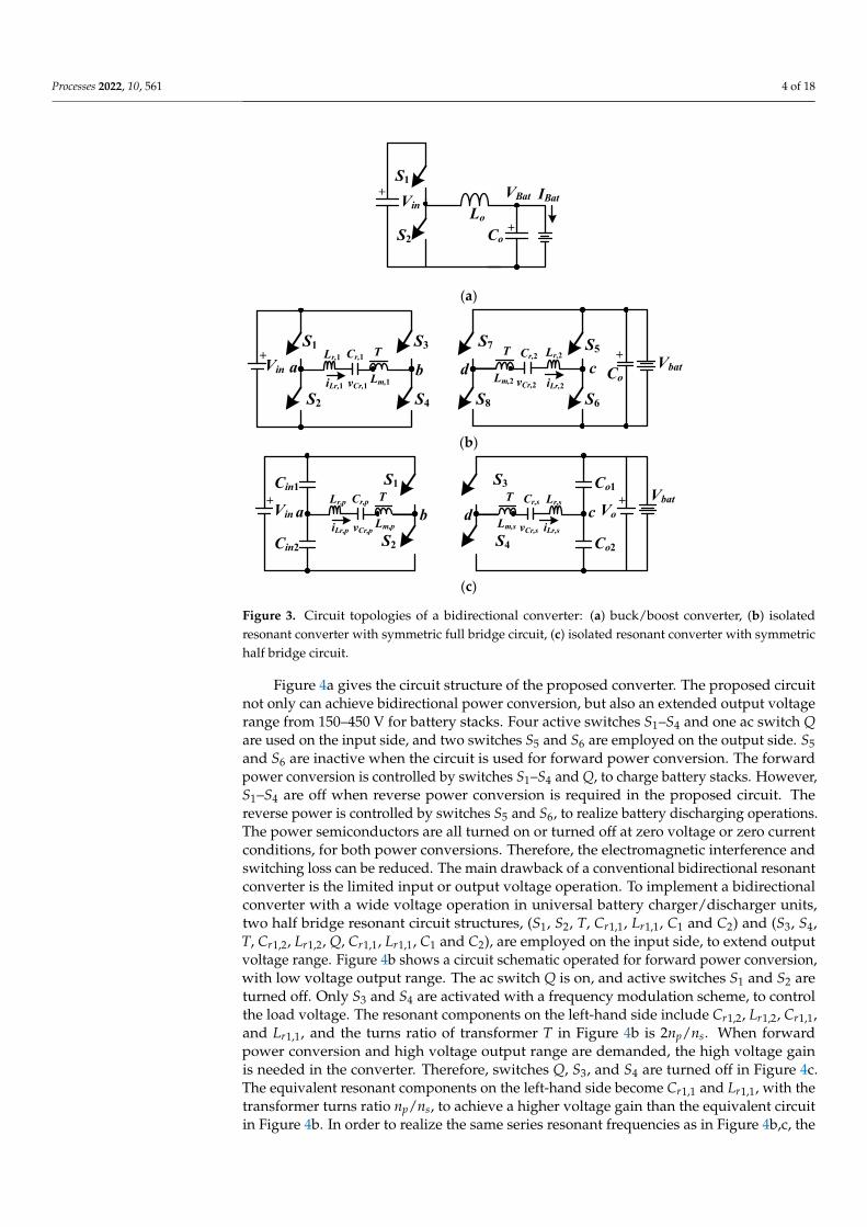
Processes 2022, 10, 561 4 of 18Processes 2022, 10, x FOR PEER REVIEW 4 of 19
S1
S2
VBat IBat+
+Co
Vin Lo
(a)
Vin
S1
S2
+S3
S4
a bTLr,1
iLr,1
Cr,1
vCr,1Lm,1
Co
S5
S6
+S7
S8
dT Lr,2
iLr,2
Cr,2
vCr,2Lm,2
c Vbat
(b)
Vin+
S1
S2
a bTLr,p
iLr,p
Cr,p
vCr,pLm,p
Cin1
Cin2
Vo+
S3
S4
cdT Lr,s
iLr,s
Cr,s
vCr,sLm,s
Co1
Co2
Vbat
(c)
Figure 3. Circuit topologies of a bidirectional converter: (a) buck/boost converter, (b) isolated reso-nant converter with symmetric full bridge circuit, (c) isolated resonant converter with symmetric half bridge circuit.
Figure 4a gives the circuit structure of the proposed converter. The proposed circuit not only can achieve bidirectional power conversion, but also an extended output voltage range from 150–450 V for battery stacks. Four active switches S1–S4 and one ac switch Q are used on the input side, and two switches S5 and S6 are employed on the output side. S5 and S6 are inactive when the circuit is used for forward power conversion. The forward power conversion is controlled by switches S1–S4 and Q, to charge battery stacks. How-ever, S1–S4 are off when reverse power conversion is required in the proposed circuit. The reverse power is controlled by switches S5 and S6, to realize battery discharging opera-tions. The power semiconductors are all turned on or turned off at zero voltage or zero current conditions, for both power conversions. Therefore, the electromagnetic interfer-ence and switching loss can be reduced. The main drawback of a conventional bidirec-tional resonant converter is the limited input or output voltage operation. To implement a bidirectional converter with a wide voltage operation in universal battery charger/dis-charger units, two half bridge resonant circuit structures, (S1, S2, T, Cr1,1, Lr1,1, C1 and C2) and (S3, S4, T, Cr1,2, Lr1,2, Q, Cr1,1, Lr1,1, C1 and C2), are employed on the input side, to extend output voltage range. Figure 4b shows a circuit schematic operated for forward power conversion, with low voltage output range. The ac switch Q is on, and active switches S1 and S2 are turned off. Only S3 and S4 are activated with a frequency modulation scheme, to control the load voltage. The resonant components on the left-hand side include Cr1,2, Lr1,2, Cr1,1, and Lr1,1, and the turns ratio of transformer T in Figure 4b is 2np/ns. When forward power conversion and high voltage output range are demanded, the high voltage gain is needed in the converter. Therefore, switches Q, S3, and S4 are turned off in Figure 4c. The equivalent resonant components on the left-hand side become Cr1,1 and Lr1,1, with the trans-former turns ratio np/ns, to achieve a higher voltage gain than the equivalent circuit in Figure 4b. In order to realize the same series resonant frequencies as in Figure 4b,c, the
Figure 3. Circuit topologies of a bidirectional converter: (a) buck/boost converter, (b) isolatedresonant converter with symmetric full bridge circuit, (c) isolated resonant converter with symmetrichalf bridge circuit.
Figure 4a gives the circuit structure of the proposed converter. The proposed circuitnot only can achieve bidirectional power conversion, but also an extended output voltagerange from 150–450 V for battery stacks. Four active switches S1–S4 and one ac switch Qare used on the input side, and two switches S5 and S6 are employed on the output side. S5and S6 are inactive when the circuit is used for forward power conversion. The forwardpower conversion is controlled by switches S1–S4 and Q, to charge battery stacks. However,S1–S4 are off when reverse power conversion is required in the proposed circuit. Thereverse power is controlled by switches S5 and S6, to realize battery discharging operations.The power semiconductors are all turned on or turned off at zero voltage or zero currentconditions, for both power conversions. Therefore, the electromagnetic interference andswitching loss can be reduced. The main drawback of a conventional bidirectional resonantconverter is the limited input or output voltage operation. To implement a bidirectionalconverter with a wide voltage operation in universal battery charger/discharger units,two half bridge resonant circuit structures, (S1, S2, T, Cr1,1, Lr1,1, C1 and C2) and (S3, S4,T, Cr1,2, Lr1,2, Q, Cr1,1, Lr1,1, C1 and C2), are employed on the input side, to extend outputvoltage range. Figure 4b shows a circuit schematic operated for forward power conversion,with low voltage output range. The ac switch Q is on, and active switches S1 and S2 areturned off. Only S3 and S4 are activated with a frequency modulation scheme, to controlthe load voltage. The resonant components on the left-hand side include Cr1,2, Lr1,2, Cr1,1,and Lr1,1, and the turns ratio of transformer T in Figure 4b is 2np/ns. When forwardpower conversion and high voltage output range are demanded, the high voltage gainis needed in the converter. Therefore, switches Q, S3, and S4 are turned off in Figure 4c.The equivalent resonant components on the left-hand side become Cr1,1 and Lr1,1, with thetransformer turns ratio np/ns, to achieve a higher voltage gain than the equivalent circuitin Figure 4b. In order to realize the same series resonant frequencies as in Figure 4b,c, the
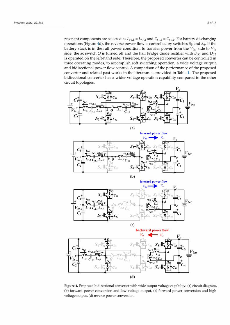
Processes 2022, 10, 561 5 of 18
resonant components are selected as Lr1,1 = Lr1,2 and Cr1,1 = Cr1,2. For battery dischargingoperations (Figure 4d), the reverse power flow is controlled by switches S5 and S6. If thebattery stack is in the full power condition, to transfer power from the Vbat side to Vinside, the ac switch Q is turned off and the half bridge diode rectifier with DS1 and DS2is operated on the left-hand side. Therefore, the proposed converter can be controlled inthree operating modes, to accomplish soft switching operation, a wide voltage output,and bidirectional power flow control. A comparison of the performance of the proposedconverter and related past works in the literature is provided in Table 1. The proposedbidirectional converter has a wider voltage operation capability compared to the othercircuit topologies.
Processes 2022, 10, x FOR PEER REVIEW 5 of 19
resonant components are selected as Lr1,1 = Lr1,2 and Cr1,1 = Cr1,2. For battery discharging operations (Figure 4d), the reverse power flow is controlled by switches S5 and S6. If the battery stack is in the full power condition, to transfer power from the Vbat side to Vin side, the ac switch Q is turned off and the half bridge diode rectifier with DS1 and DS2 is operated on the left-hand side. Therefore, the proposed converter can be controlled in three oper-ating modes, to accomplish soft switching operation, a wide voltage output, and bidirec-tional power flow control. A comparison of the performance of the proposed converter and related past works in the literature is provided in Table 1. The proposed bidirectional converter has a wider voltage operation capability compared to the other circuit topolo-gies.
Vin Qc
+
bT
Lr1,1
iLr1 vCr1,1
Lm,1
Vbat
S1
S2
C1
C2+
+
Vo
e
S5
S6
dLr2
iLr2
Cr2vCr2
Lm,2
C3
C4+
+
a
S3
S4
vCr1,2
Lr1,2 Cr1,2Cr1,1
CS1
CS2
CS3
CS4
CS5
CS6
DS1
DS2 DS6
DS5
DS4
DS3
np1np2
nS
(a)
Vo
forward power flowVin
Vin Qc
+
bT
Lr1,1
iLr1 vCr1,1
Lm,1
Vbat
S1
S2
C1
C2+
+
Vo
e
S5
S6
dLr2
iLr2
Cr2vCr2
Lm,2
C3
C4+
+
a
S3
S4
vCr1,2
Lr1,2 Cr1,2Cr1,1
CS1
CS2
CS3
CS4
CS5
CS6
DS1
DS2 DS6
DS5
DS4
DS3
nS
np2np1
(b)
Vo
forward power flowVin
Vin Qc
+
bT
Lr1,1
iLr1 vCr1,1
Lm,1
Vbat
S1
S2
C1
C2+
+
Vo
e
S5
S6
dLr2
iLr2
Cr2vCr2
Lm,2
C3
C4+
+
a
S3
S4
vCr1,2
Lr1,2 Cr1,2Cr1,1
CS1
CS2
CS3
CS4
CS5
CS6
DS1
DS2 DS6
DS5
DS4
DS3
np1
ns
(c)
VoVin
backward power flow
Vin Qc
+
bT
Lr1,1
iLr1 vCr1,1
Lm,1
Vbat
S1
S2
C1
C2+
+
Vo
e
S5
S6
dLr2
iLr2
Cr2vCr2
Lm,2
C3
C4+
+
a
S3
S4
vCr1,2
Lr1,2 Cr1,2Cr1,1
CS1
CS2
CS3
CS4
CS5
CS6
DS1
DS2 DS6
DS5
DS4
DS3
np1
ns
(d)
Figure 4. Proposed bidirectional converter with wide output voltage capability: (a) circuit diagram, (b) forward power conversion and low voltage output, (c) forward power conversion and high volt-age output, (d) reverse power conversion.
Figure 4. Proposed bidirectional converter with wide output voltage capability: (a) circuit diagram,(b) forward power conversion and low voltage output, (c) forward power conversion and highvoltage output, (d) reverse power conversion.

Processes 2022, 10, 561 6 of 18
Table 1. Comparison between the presented circuit and the other bidirectional converters.
Primary-Side Secondary-Side Input/OutputVoltages Power Flow Direction Control Scheme
Proposedcircuit
Half-bridgecircuit Half-bridge circuit Vin = 400 V
Vo = 150–450 V
Voltagestep-up/step-down for
bidirectional power flowFrequency control
Circuitstructure in [9]
Half-bridgecircuit Half-bridge circuit Vin = 48 V
Vo = 24–30 V
Voltage step-down forforward power flow and
voltage step-up forreverse power flow
Phase shift + PWMcontrol
Circuitstructure in
[11]
Full-bridgecircuit Full-bridge circuit Vin = 400 V
Vo =400 V
Voltagestep-up/step-down for
bidirectional power flow
Phase shift + PWMcontrol
Circuitstructure in
[13]
Full-bridgecircuit Full-bridge circuit Vin = 382–408 V
Vo = 400 V
Voltagestep-up/step-down for
bidirectional power flowFrequency control
Circuitstructure in
[15]
Cascadehalf-bridge
circuit
Parallelcenter-tapped
rectifier
Vin = 750–800 VVo = 24 V
Voltagestep-up/step-down for
forward power flowFrequency control
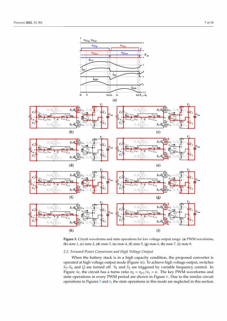
2.1. Forward Power Conversion and Low Voltage Output
When a battery stack has a low capacity or depleted condition, the converter iscontrolled in low voltage output mode (Figure 4b). Q turns on and S1, S2, S5, and S6 areoff under low voltage output mode. S3 and S4 are operated with frequency modulation,to control the battery voltage or battery charging current. The transformer turns ratioin Figure 4b is n1 = (np1 + np2)/ns = 2np/ns = 2n, where np1 = np2 = np and n = np/ns.Figure 5a shows the main PWM signals of the proposed converter under a fsw (switchingfrequency) < fr (resonant frequency) condition. The circuit parameters are assumed asLr1,1 = Lr1,2 = n2Lr2 and Cr1,1 = Cr1,2 = Cr2/n2. Based on the above assumption, the resonantfrequencies under forward and reverse power flow operations are identical. Figure 5b–ishow the operating circuits for eight operating states.
State 1 [t0 ≤ t < t1]: For t = t0, the output capacitor voltage vCS3 is decreased to zero voltageand the diode DS3 becomes forward biased, owing to iLr1(t0) being negative. Atthis time, S1 is turned on, to have zero voltage switching. Since iLr2 is positive, theantipallel diodes DS5 and DS6 are conducting.
State 2 [t1 ≤ t < t2]: The primary current iLr1 becomes positive value after t1. Therefore, iLr1will flow through switch S3 instead of diode DS3. In this state, the forward power flowis from C1 to C3. The leg voltages are Vac = VC1 = Vin/2 and Vde = VC3 = Vo/2. The se-ries resonant frequency is fr = 1/(2π
√(Lr1,1 + Lr1,2)(Cr1,1Cr1,2)/(Cr1,1 + Cr1,2) ) =
1/(2π√
Lr1,1Cr1,1). If fsw < (or >) fr, then the next state operation of the proposedcircuit will go to state 3 (or state 4).
State 3 [t2 ≤ t < t3]: At time t2, iLr2 becomes zero at time t2 and DS5 becomes off. iLr1 flowsthrough S3, Lm,1, Cr1,1, Lr1,1, Cr1,2, Lr1,2, and C1.
State 4 [t3 ≤ t < t4]: At time t3, S3 turns off. iLr1 charges CS3 and discharges CS4. VCS4 = 0 at t4.State 5 [t4 ≤ t < t5]: vCS4 = 0 at t4 and DS4 becomes forward biased due to iLr1(t4) > 0. At this
moment, S4 turns on under zero voltage. In state 5, iLr2 < 0 and DS6 is conductingto charge C4.
State 6 [t5 ≤ t < t6]: Since Vac = −VC2 = −Vin/2, iLr1 is decreased and becomes negative attime t5. Then, the primary current iLr1 will flow through S4 instead of DS4. Forwardpower flow is from C2 to charge C4.
State 7 [t6 ≤ t < t7]: iLr2 = 0 at t = t6 and DS6 turns off. The primary side current iLr1 flowsthrough C2, Lr1,1, Cr1,1, Lm,1, Lr1,2, Cr1,2, and S4.
State 8 [t7 ≤ t < Tsw+t0]: S4 turns off at t = t7. Then, CS3 is discharged and CS4 is chargedby current iLr1. This state is terminated at Tsw + t0.
Processes 2022, 10, 561 7 of 18
Processes 2022, 10, x FOR PEER REVIEW 7 of 19
State 5 [t4 ≤ t < t5]: vCS4 = 0 at t4 and DS4 becomes forward biased due to iLr1(t4) > 0. At this moment, S4 turns on under zero voltage. In state 5, iLr2 < 0 and DS6 is conducting to charge C4.
State 6 [t5 ≤ t < t6]: Since Vac = −VC2 = −Vin/2, iLr1 is decreased and becomes negative at time t5. Then, the primary current iLr1 will flow through S4 instead of DS4. Forward power flow is from C2 to charge C4.
State 7 [t6 ≤ t < t7]: iLr2 = 0 at t = t6 and DS6 turns off. The primary side current iLr1 flows through C2, Lr1,1, Cr1,1, Lm,1, Lr1,2, Cr1,2, and S4.
State 8 [t7 ≤ t < Tsw+t0]: S4 turns off at t = t7. Then, CS3 is discharged and CS4 is charged by current iLr1. This state is terminated at Tsw + t0.
vS3,g
tt0
iLr1
Vin
t1 t2t3 t4 t7
vS3,ce
vS4,g
vS4,ce
iS3
iS4iDS5
iDS6
Tsw+t0t5 t6
vS1,g, vS2,g
(a)
Vin Qc
+
bT
Lr1,1
iLr1 vCr1,1
Lm,1
Vbat
S1
S2
C1
C2+
+
Vo
e
S5
S6
dLr2
iLr2
Cr2vCr2
Lm,2
C3
C4+
+
a
S3
S4
vCr1,2
Lr1,2 Cr1,2Cr1,1
CS1
CS2
CS3
CS4
CS5
CS6
DS1
DS2 DS6
DS5
DS4
DS3
Vin Qc
+
bT
Lr1,1
iLr1 vCr1,1
Lm,1
Vbat
S1
S2
C1
C2+
+
Vo
e
S5
S6
dLr2
iLr2
Cr2vCr2
Lm,2
C3
C4+
+
a
S3
S4
vCr1,2
Lr1,2 Cr1,2Cr1,1
CS1
CS2
CS3
CS4
CS5
CS6
DS1
DS2 DS6
DS5
DS4
DS3
(b) (c)
Vin Qc
+
bT
Lr1,1
iLr1 vCr1,1
Lm,1
Vbat
S1
S2
C1
C2+
+
Vo
e
S5
S6
dLr2
iLr2
Cr2vCr2
Lm,2
C3
C4+
+
a
S3
S4
vCr1,2
Lr1,2 Cr1,2Cr1,1
CS1
CS2
CS3
CS4
CS5
CS6
DS1
DS2 DS6
DS5
DS4
DS3
Vin Qc
+
bT
Lr1,1
iLr1 vCr1,1
Lm,1
Vbat
S1
S2
C1
C2+
+
Vo
e
S5
S6
dLr2
iLr2
Cr2vCr2
Lm,2
C3
C4+
+
a
S3
S4
vCr1,2
Lr1,2 Cr1,2Cr1,1
CS1
CS2
CS3
CS4
CS5
CS6
DS1
DS2 DS6
DS5
DS4
DS3
(d) (e)
Vin Qc
+
bT
Lr1,1
iLr1 vCr1,1
Lm,1
Vbat
S1
S2
C1
C2+
+
Vo
e
S5
S6
dLr2
iLr2
Cr2vCr2
Lm,2
C3
C4+
+
a
S3
S4
vCr1,2
Lr1,2 Cr1,2Cr1,1
CS1
CS2
CS3
CS4
CS5
CS6
DS1
DS2 DS6
DS5
DS4
DS3
Vin Qc
+
bT
Lr1,1
iLr1 vCr1,1
Lm,1
Vbat
S1
S2
C1
C2+
+
Vo
e
S5
S6
dLr2
iLr2
Cr2vCr2
Lm,2
C3
C4+
+
a
S3
S4
vCr1,2
Lr1,2 Cr1,2Cr1,1
CS1
CS2
CS3
CS4
CS5
CS6
DS1
DS2 DS6
DS5
DS4
DS3
(f) (g)
Vin Qc
+
bT
Lr1,1
iLr1 vCr1,1
Lm,1
Vbat
S1
S2
C1
C2+
+
Vo
e
S5
S6
dLr2
iLr2
Cr2vCr2
Lm,2
C3
C4+
+
a
S3
S4
vCr1,2
Lr1,2 Cr1,2Cr1,1
CS1
CS2
CS3
CS4
CS5
CS6
DS1
DS2 DS6
DS5
DS4
DS3
Vin Qc
+
bT
Lr1,1
iLr1 vCr1,1
Lm,1
Vbat
S1
S2
C1
C2+
+
Vo
e
S5
S6
dLr2
iLr2
Cr2vCr2
Lm,2
C3
C4+
+
a
S3
S4
vCr1,2
Lr1,2 Cr1,2Cr1,1
CS1
CS2
CS3
CS4
CS5
CS6
DS1
DS2 DS6
DS5
DS4
DS3
(h) (i)
Figure 5. Circuit waveforms and state operations for low voltage output range: (a) PWM waveforms, (b) state 1, (c) state 2, (d) state 3, (e) state 4, (f) state 5, (g) state 6, (h) state 7, (i) state 8.
Figure 5. Circuit waveforms and state operations for low voltage output range: (a) PWM waveforms,(b) state 1, (c) state 2, (d) state 3, (e) state 4, (f) state 5, (g) state 6, (h) state 7, (i) state 8.
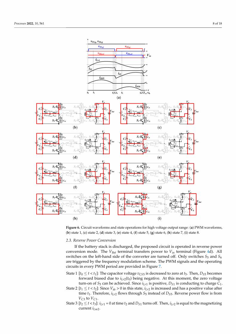
2.2. Forward Power Conversion and High Voltage Output
When the battery stack is in a high capacity condition, the proposed converter isoperated at high voltage output mode (Figure 4c). To achieve high voltage output, switchesS3–S6 and Q are turned off. S1 and S2 are triggered by variable frequency control. InFigure 4c, the circuit has a turns ratio n2 = np1/ns = n. The key PWM waveforms andstate operations in every PWM period are shown in Figure 6. Due to the similar circuitoperations in Figures 5 and 6, the state operations in this mode are neglected in this section.
Processes 2022, 10, 561 8 of 18
Processes 2022, 10, x FOR PEER REVIEW 8 of 19
2.2. Forward Power Conversion and High Voltage Output When the battery stack is in a high capacity condition, the proposed converter is op-
erated at high voltage output mode (Figure 4c). To achieve high voltage output, switches S3–S6 and Q are turned off. S1 and S2 are triggered by variable frequency control. In Figure 4c, the circuit has a turns ratio n2 = np1/ns = n. The key PWM waveforms and state opera-tions in every PWM period are shown in Figure 6. Due to the similar circuit operations in Figures 5 and 6, the state operations in this mode are neglected in this section.
vS1,g
tt0
iLr1
Vin
t1 t2t3t4 t7
vS1,ce
vS2,g
vS2,ce
iS1
iS2iDS5
iDS6
Tsw+t0t5 t6
vS3,g, vS4,g
(a)
Vin Qc
+
bT
Lr1,1
iLr1 vCr1,1
Lm,1
Vbat
S1
S2
C1
C2+
+
Vo
e
S5
S6
dLr2
iLr2
Cr2vCr2
Lm,2
C3
C4+
+
a
S3
S4
vCr1,2
Lr1,2 Cr1,2Cr1,1
CS1
CS2
CS3
CS4
CS5
CS6
DS1
DS2 DS6
DS5
DS4
DS3
Vin Qc
+
bT
Lr1,1
iLr1 vCr1,1
Lm,1
Vbat
S1
S2
C1
C2+
+
Vo
e
S5
S6
dLr2
iLr2
Cr2vCr2
Lm,2
C3
C4+
+
a
S3
S4
vCr1,2
Lr1,2 Cr1,2Cr1,1
CS1
CS2
CS3
CS4
CS5
CS6
DS1
DS2 DS6
DS5
DS4
DS3
(b) (c)
Vin Qc
+
bT
Lr1,1
iLr1 vCr1,1
Lm,1
Vbat
S1
S2
C1
C2+
+
Vo
e
S5
S6
dLr2
iLr2
Cr2vCr2
Lm,2
C3
C4+
+
a
S3
S4
vCr1,2
Lr1,2 Cr1,2Cr1,1
CS1
CS2
CS3
CS4
CS5
CS6
DS1
DS2 DS6
DS5
DS4
DS3
Vin Qc
+
bT
Lr1,1
iLr1 vCr1,1
Lm,1
Vbat
S1
S2
C1
C2+
+
Vo
e
S5
S6
dLr2
iLr2
Cr2vCr2
Lm,2
C3
C4+
+
a
S3
S4
vCr1,2
Lr1,2 Cr1,2Cr1,1
CS1
CS2
CS3
CS4
CS5
CS6
DS1
DS2 DS6
DS5
DS4
DS3
(d) (e)
Vin Qc
+
bT
Lr1,1
iLr1 vCr1,1
Lm,1
Vbat
S1
S2
C1
C2+
+
Vo
e
S5
S6
dLr2
iLr2
Cr2vCr2
Lm,2
C3
C4+
+
a
S3
S4
vCr1,2
Lr1,2 Cr1,2Cr1,1
CS1
CS2
CS3
CS4
CS5
CS6
DS1
DS2 DS6
DS5
DS4
DS3
Vin Qc
+
bT
Lr1,1
iLr1 vCr1,1
Lm,1
Vbat
S1
S2
C1
C2+
+
Vo
e
S5
S6
dLr2
iLr2
Cr2vCr2
Lm,2
C3
C4+
+
a
S3
S4
vCr1,2
Lr1,2 Cr1,2Cr1,1
CS1
CS2
CS3
CS4
CS5
CS6
DS1
DS2 DS6
DS5
DS4
DS3
(f) (g)
Vin Qc
+
bT
Lr1,1
iLr1 vCr1,1
Lm,1
Vbat
S1
S2
C1
C2+
+
Vo
e
S5
S6
dLr2
iLr2
Cr2vCr2
Lm,2
C3
C4+
+
a
S3
S4
vCr1,2
Lr1,2 Cr1,2Cr1,1
CS1
CS2
CS3
CS4
CS5
CS6
DS1
DS2 DS6
DS5
DS4
DS3
Vin Qc
+
bT
Lr1,1
iLr1 vCr1,1
Lm,1
Vbat
S1
S2
C1
C2+
+
Vo
e
S5
S6
dLr2
iLr2
Cr2vCr2
Lm,2
C3
C4+
+
a
S3
S4
vCr1,2
Lr1,2 Cr1,2Cr1,1
CS1
CS2
CS3
CS4
CS5
CS6
DS1
DS2 DS6
DS5
DS4
DS3
(h) (i)
Figure 6. Circuit waveforms and state operations for high voltage output range: (a) PWM wave-forms, (b) state 1, (c) state 2, (d) state 3, (e) state 4, (f) state 5, (g) state 6, (h) state 7, (i) state 8.
Figure 6. Circuit waveforms and state operations for high voltage output range: (a) PWM waveforms,(b) state 1, (c) state 2, (d) state 3, (e) state 4, (f) state 5, (g) state 6, (h) state 7, (i) state 8.
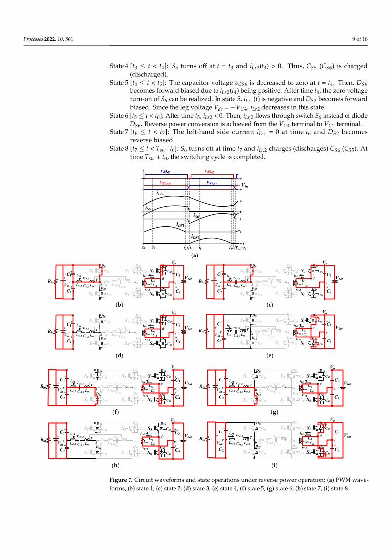
2.3. Reverse Power Conversion
If the battery stack is discharged, the proposed circuit is operated in reverse powerconversion mode. The VBat terminal transfers power to Vin terminal (Figure 4d). Allswitches on the left-hand side of the converter are turned off. Only switches S5 and S6are triggered by the frequency modulation scheme. The PWM signals and the operatingcircuits in every PWM period are provided in Figure 7.
State 1 [t0 ≤ t < t1]: The capacitor voltage vCS5 is decreased to zero at t5. Then, DS5 becomesforward biased due to iLr2(t0) being negative. At this moment, the zero voltageturn-on of S5 can be achieved. Since iLr1 is positive, DS1 is conducting to charge C1.
State 2 [t1 ≤ t < t2]: Since Vde > 0 in this state, iLr2 is increased and has a positive value aftertime t1. Therefore, iLr2 flows through S5 instead of DS5. Reverse power flow is fromVC3 to VC1.
State 3 [t2 ≤ t < t3]: iLr1 = 0 at time t2 and DS1 turns off. Then, iLr2 is equal to the magnetizingcurrent iLm2.
Processes 2022, 10, 561 9 of 18
State 4 [t3 ≤ t < t4]: S5 turns off at t = t3 and iLr2(t3) > 0. Thus, CS5 (CS6) is charged(discharged).
State 5 [t4 ≤ t < t5]: The capacitor voltage vCS6 is decreased to zero at t = t4. Then, DS6becomes forward biased due to iLr2(t4) being positive. After time t4, the zero voltageturn-on of S6 can be realized. In state 5, iLr1(t) is negative and DS2 becomes forwardbiased. Since the leg voltage Vde = −VC4, iLr2 decreases in this state.
State 6 [t5 ≤ t < t6]: After time t5, iLr2 < 0. Then, iLr,2 flows through switch S6 instead of diodeDS6. Reverse power conversion is achieved from the VC4 terminal to VC2 terminal.
State 7 [t6 ≤ t < t7]: The left-hand side current iLr1 = 0 at time t6 and DS2 becomesreverse biased.
State 8 [t7 ≤ t < Tsw+t0]: S6 turns off at time t7 and iLr,2 charges (discharges) CS6 (CS5). Attime Tsw + t0, the switching cycle is completed.
Processes 2022, 10, x FOR PEER REVIEW 9 of 19
2.3. Reverse Power Conversion If the battery stack is discharged, the proposed circuit is operated in reverse power
conversion mode. The VBat terminal transfers power to Vin terminal (Figure 4d). All switches on the left-hand side of the converter are turned off. Only switches S5 and S6 are triggered by the frequency modulation scheme. The PWM signals and the operating cir-cuits in every PWM period are provided in Figure 7. State 1 [t0 ≤ t < t1]: The capacitor voltage vCS5 is decreased to zero at t5. Then, DS5 becomes
forward biased due to iLr2(t0) being negative. At this moment, the zero voltage turn-on of S5 can be achieved. Since iLr1 is positive, DS1 is conducting to charge C1.
State 2 [t1 ≤ t < t2]: Since Vde > 0 in this state, iLr2 is increased and has a positive value after time t1. Therefore, iLr2 flows through S5 instead of DS5. Reverse power flow is from VC3 to VC1.
State 3 [t2 ≤ t < t3]: iLr1 = 0 at time t2 and DS1 turns off. Then, iLr2 is equal to the magnetizing current iLm2.
State 4 [t3 ≤ t < t4]: S5 turns off at t = t3 and iLr2 (t3) > 0. Thus, CS5 (CS6) is charged (discharged). State 5 [t4 ≤ t < t5]: The capacitor voltage vCS6 is decreased to zero at t = t4. Then, DS6 becomes
forward biased due to iLr2(t4) being positive. After time t4, the zero voltage turn-on of S6 can be realized. In state 5, iLr1(t) is negative and DS2 becomes forward biased. Since the leg voltage Vde = −VC4, iLr2 decreases in this state.
State 6 [t5 ≤ t < t6]: After time t5, iLr2 < 0. Then, iLr,2 flows through switch S6 instead of diode DS6. Reverse power conversion is achieved from the VC4 terminal to VC2 terminal.
State 7 [t6 ≤ t < t7]: The left-hand side current iLr1 = 0 at time t6 and DS2 becomes reverse biased.
State 8 [t7 ≤ t < Tsw+t0]: S6 turns off at time t7 and iLr,2 charges (discharges) CS6 (CS5). At time Tsw + t0, the switching cycle is completed.
vS5,g
tt0
iLr2
Vin
t1 t2t3 t4 t7
vS5,ce
vS6,g
vS6,ce
iS5
iS6
iDS1
iDS2
Tsw+t0t5 t6 (a)
Vin Qc
+
bT
Lr1,1
iLr1 vCr1,1
Lm,1
Vbat
S1
S2
C1
C2+
+
Vo
e
S5
S6
dLr2
iLr2
Cr2vCr2
Lm,2
C3
C4+
+
a
S3
S4
vCr1,2
Lr1,2 Cr1,2Cr1,1
CS1
CS2
CS3
CS4
CS5
CS6
DS1
DS2 DS6
DS5
DS4
DS3
Rin
Vin Qc
+
bT
Lr1,1
iLr1 vCr1,1
Lm,1
Vbat
S1
S2
C1
C2+
+
Vo
e
S5
S6
dLr2
iLr2
Cr2vCr2
Lm,2
C3
C4+
+
a
S3
S4
vCr1,2
Lr1,2 Cr1,2Cr1,1
CS1
CS2
CS3
CS4
CS5
CS6
DS1
DS2 DS6
DS5
DS4
DS3
Rin
(b) (c)
Vin Qc
+
bT
Lr1,1
iLr1 vCr1,1
Lm,1
Vbat
S1
S2
C1
C2+
+
Vo
e
S5
S6
dLr2
iLr2
Cr2vCr2
Lm,2
C3
C4+
+
a
S3
S4
vCr1,2
Lr1,2 Cr1,2Cr1,1
CS1
CS2
CS3
CS4
CS5
CS6
DS1
DS2 DS6
DS5
DS4
DS3
Rin
Vin Qc
+
bT
Lr1,1
iLr1 vCr1,1
Lm,1
Vbat
S1
S2
C1
C2+
+
Vo
e
S5
S6
dLr2
iLr2
Cr2vCr2
Lm,2
C3
C4+
+
a
S3
S4
vCr1,2
Lr1,2 Cr1,2Cr1,1
CS1
CS2
CS3
CS4
CS5
CS6
DS1
DS2 DS6
DS5
DS4
DS3
Rin
(d) (e)
Processes 2022, 10, x FOR PEER REVIEW 10 of 19
Vin Qc
+
bT
Lr1,1
iLr1 vCr1,1
Lm,1
Vbat
S1
S2
C1
C2+
+
Vo
e
S5
S6
dLr2
iLr2
Cr2vCr2
Lm,2
C3
C4+
+
a
S3
S4
vCr1,2
Lr1,2 Cr1,2Cr1,1
CS1
CS2
CS3
CS4
CS5
CS6
DS1
DS2 DS6
DS5
DS4
DS3
Rin
Vin Qc
+
bT
Lr1,1
iLr1 vCr1,1
Lm,1
Vbat
S1
S2
C1
C2+
+
Vo
e
S5
S6
dLr2
iLr2
Cr2vCr2
Lm,2
C3
C4+
+
a
S3
S4
vCr1,2
Lr1,2 Cr1,2Cr1,1
CS1
CS2
CS3
CS4
CS5
CS6
DS1
DS2 DS6
DS5
DS4
DS3
Rin
(f) (g)
Vin Qc
+
bT
Lr1,1
iLr1 vCr1,1
Lm,1
Vbat
S1
S2
C1
C2+
+
Vo
e
S5
S6
dLr2
iLr2
Cr2vCr2
Lm,2
C3
C4+
+
a
S3
S4
vCr1,2
Lr1,2 Cr1,2Cr1,1
CS1
CS2
CS3
CS4
CS5
CS6
DS1
DS2 DS6
DS5
DS4
DS3
Rin
Vin Qc
+
bT
Lr1,1
iLr1 vCr1,1
Lm,1
Vbat
S1
S2
C1
C2+
+
Vo
e
S5
S6
dLr2
iLr2
Cr2vCr2
Lm,2
C3
C4+
+
a
S3
S4
vCr1,2
Lr1,2 Cr1,2Cr1,1
CS1
CS2
CS3
CS4
CS5
CS6
DS1
DS2 DS6
DS5
DS4
DS3
Rin
(h) (i)
Figure 7. Circuit waveforms and state operations under reverse power operation: (a) PWM wave-forms, (b) state 1, (c) state 2, (d) state 3, (e) state 4, (f) state 5, (g) state 6, (h) state 7, (i) state 8.
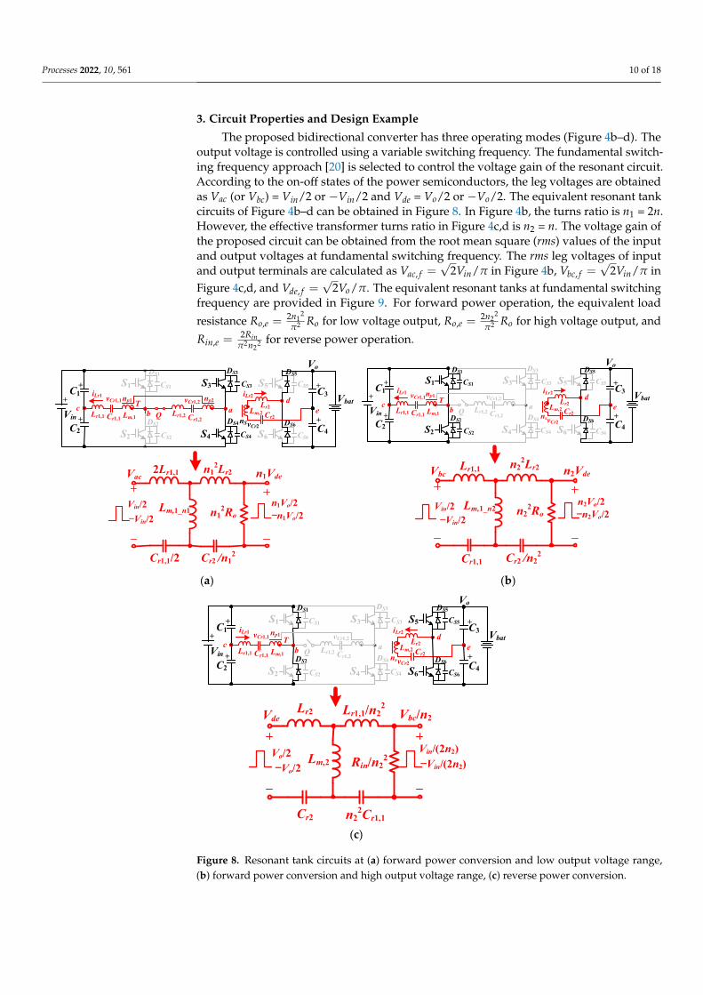
3. Circuit Properties and Design Example The proposed bidirectional converter has three operating modes (Figure 4b–d). The
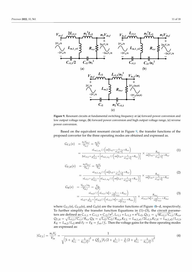
output voltage is controlled using a variable switching frequency. The fundamental switching frequency approach [20] is selected to control the voltage gain of the resonant circuit. According to the on-off states of the power semiconductors, the leg voltages are obtained as Vac (or Vbc) = Vin/2 or −Vin/2 and Vde = Vo/2 or −Vo/2. The equivalent resonant tank circuits of Figure 4b–d can be obtained in Figure 8. In Figure 4b, the turns ratio is n1 = 2n. However, the effective transformer turns ratio in Figure 4c,d is n2 = n. The voltage gain of the proposed circuit can be obtained from the root mean square (rms) values of the input and output voltages at fundamental switching frequency. The rms leg voltages of input and output terminals are calculated as π/2, infac VV = in Figure 4b, π/2, infbc VV = in
Figure 4c,d, and π/2, ofde VV = . The equivalent resonant tanks at fundamental switching frequency are provided in Figure 9. For forward power operation, the equivalent load
resistance oeo RnR 2
21
,2π
= for low voltage output, oeo RnR 2
22
,2π
= for high voltage output,
and 22
2,2
nRR in
ein π= for reverse power operation.
Vin Qc
+
bT
Lr1,1
iLr1 vCr1,1
Lm,1
Vbat
S1
S2
C1
C2+
+
Vo
e
S5
S6
dLr2
iLr2
Cr2vCr2
Lm,2
C3
C4+
+
a
S3
S4
vCr1,2
Lr1,2 Cr1,2Cr1,1
CS1
CS2
CS3
CS4
CS5
CS6
DS1
DS2 DS6
DS5
DS4
DS3
nS
np2np1
2Lr1,1 n12Lr2
Cr2 /n12
Vac n1Vde
n1Vo/2Vin/2−Vin/2 n1
2Ro −n1Vo/2
Cr1,1/2
Lm,1_n1 Lm,1_n2
Cr1,1
Lr1,1 n22Lr2
Cr2 /n22
Vbc n2Vde
n2Vo/2Vin/2−Vin/2
n22Ro −n2Vo/2
Vin Qc
+
bT
Lr1,1
iLr1 vCr1,1
Lm,1
Vbat
S1
S2
C1
C2+
+
Vo
e
S5
S6
dLr2
iLr2
Cr2vCr2
Lm,2
C3
C4+
+
a
S3
S4
vCr1,2
Lr1,2 Cr1,2Cr1,1
CS1
CS2
CS3
CS4
CS5
CS6
DS1
DS2 DS6
DS5
DS4
DS3
np1
ns
(a) (b)
Figure 7. Circuit waveforms and state operations under reverse power operation: (a) PWM wave-forms, (b) state 1, (c) state 2, (d) state 3, (e) state 4, (f) state 5, (g) state 6, (h) state 7, (i) state 8.
Processes 2022, 10, 561 10 of 18
3. Circuit Properties and Design Example
The proposed bidirectional converter has three operating modes (Figure 4b–d). Theoutput voltage is controlled using a variable switching frequency. The fundamental switch-ing frequency approach [20] is selected to control the voltage gain of the resonant circuit.According to the on-off states of the power semiconductors, the leg voltages are obtainedas Vac (or Vbc) = Vin/2 or −Vin/2 and Vde = Vo/2 or −Vo/2. The equivalent resonant tankcircuits of Figure 4b–d can be obtained in Figure 8. In Figure 4b, the turns ratio is n1 = 2n.However, the effective transformer turns ratio in Figure 4c,d is n2 = n. The voltage gain ofthe proposed circuit can be obtained from the root mean square (rms) values of the inputand output voltages at fundamental switching frequency. The rms leg voltages of inputand output terminals are calculated as Vac, f =
√2Vin/π in Figure 4b, Vbc, f =
√2Vin/π in
Figure 4c,d, and Vde, f =√
2Vo/π. The equivalent resonant tanks at fundamental switchingfrequency are provided in Figure 9. For forward power operation, the equivalent load
resistance Ro,e =2n1
2
π2 Ro for low voltage output, Ro,e =2n2
2
π2 Ro for high voltage output, and
Rin,e =2Rin
π2n22 for reverse power operation.
Processes 2022, 10, x FOR PEER REVIEW 10 of 19
Vin Qc
+
bT
Lr1,1
iLr1 vCr1,1
Lm,1
Vbat
S1
S2
C1
C2+
+
Vo
e
S5
S6
dLr2
iLr2
Cr2vCr2
Lm,2
C3
C4+
+
a
S3
S4
vCr1,2
Lr1,2 Cr1,2Cr1,1
CS1
CS2
CS3
CS4
CS5
CS6
DS1
DS2 DS6
DS5
DS4
DS3
Rin
Vin Qc
+
bT
Lr1,1
iLr1 vCr1,1
Lm,1
Vbat
S1
S2
C1
C2+
+
Vo
e
S5
S6
dLr2
iLr2
Cr2vCr2
Lm,2
C3
C4+
+
a
S3
S4
vCr1,2
Lr1,2 Cr1,2Cr1,1
CS1
CS2
CS3
CS4
CS5
CS6
DS1
DS2 DS6
DS5
DS4
DS3
Rin
(f) (g)
Vin Qc
+
bT
Lr1,1
iLr1 vCr1,1
Lm,1
Vbat
S1
S2
C1
C2+
+
Vo
e
S5
S6
dLr2
iLr2
Cr2vCr2
Lm,2
C3
C4+
+
a
S3
S4
vCr1,2
Lr1,2 Cr1,2Cr1,1
CS1
CS2
CS3
CS4
CS5
CS6
DS1
DS2 DS6
DS5
DS4
DS3
Rin
Vin Qc
+
bT
Lr1,1
iLr1 vCr1,1
Lm,1
Vbat
S1
S2
C1
C2+
+
Vo
e
S5
S6
dLr2
iLr2
Cr2vCr2
Lm,2
C3
C4+
+
a
S3
S4
vCr1,2
Lr1,2 Cr1,2Cr1,1
CS1
CS2
CS3
CS4
CS5
CS6
DS1
DS2 DS6
DS5
DS4
DS3
Rin
(h) (i)
Figure 7. Circuit waveforms and state operations under reverse power operation: (a) PWM wave-forms, (b) state 1, (c) state 2, (d) state 3, (e) state 4, (f) state 5, (g) state 6, (h) state 7, (i) state 8.
3. Circuit Properties and Design Example The proposed bidirectional converter has three operating modes (Figure 4b–d). The
output voltage is controlled using a variable switching frequency. The fundamental switching frequency approach [20] is selected to control the voltage gain of the resonant circuit. According to the on-off states of the power semiconductors, the leg voltages are obtained as Vac (or Vbc) = Vin/2 or −Vin/2 and Vde = Vo/2 or −Vo/2. The equivalent resonant tank circuits of Figure 4b–d can be obtained in Figure 8. In Figure 4b, the turns ratio is n1 = 2n. However, the effective transformer turns ratio in Figure 4c,d is n2 = n. The voltage gain of the proposed circuit can be obtained from the root mean square (rms) values of the input and output voltages at fundamental switching frequency. The rms leg voltages of input and output terminals are calculated as π/2, infac VV = in Figure 4b, π/2, infbc VV = in
Figure 4c,d, and π/2, ofde VV = . The equivalent resonant tanks at fundamental switching frequency are provided in Figure 9. For forward power operation, the equivalent load
resistance oeo RnR 2
21
,2π
= for low voltage output, oeo RnR 2
22
,2π
= for high voltage output,
and 22
2,2
nRR in
ein π= for reverse power operation.
Vin Qc
+
bT
Lr1,1
iLr1 vCr1,1
Lm,1
Vbat
S1
S2
C1
C2+
+
Vo
e
S5
S6
dLr2
iLr2
Cr2vCr2
Lm,2
C3
C4+
+
a
S3
S4
vCr1,2
Lr1,2 Cr1,2Cr1,1
CS1
CS2
CS3
CS4
CS5
CS6
DS1
DS2 DS6
DS5
DS4
DS3
nS
np2np1
2Lr1,1 n12Lr2
Cr2 /n12
Vac n1Vde
n1Vo/2Vin/2−Vin/2 n1
2Ro −n1Vo/2
Cr1,1/2
Lm,1_n1 Lm,1_n2
Cr1,1
Lr1,1 n22Lr2
Cr2 /n22
Vbc n2Vde
n2Vo/2Vin/2−Vin/2
n22Ro −n2Vo/2
Vin Qc
+
bT
Lr1,1
iLr1 vCr1,1
Lm,1
Vbat
S1
S2
C1
C2+
+
Vo
e
S5
S6
dLr2
iLr2
Cr2vCr2
Lm,2
C3
C4+
+
a
S3
S4
vCr1,2
Lr1,2 Cr1,2Cr1,1
CS1
CS2
CS3
CS4
CS5
CS6
DS1
DS2 DS6
DS5
DS4
DS3
np1
ns
(a) (b)
Processes 2022, 10, x FOR PEER REVIEW 11 of 19
Lm,2
Cr2
Lr2 Lr1,1/n22
Vde Vbc/n2
Rin/n22Vo/2
−Vo/2
Vin/(2n2)
n22Cr1,1
−Vin/(2n2)
Vin Qc
+
bT
Lr1,1
iLr1 vCr1,1
Lm,1
Vbat
S1
S2
C1
C2+
+
Vo
e
S5
S6
dLr2
iLr2
Cr2vCr2
Lm,2
C3
C4+
+
a
S3
S4
vCr1,2
Lr1,2 Cr1,2Cr1,1
CS1
CS2
CS3
CS4
CS5
CS6
DS1
DS2 DS6
DS5
DS4
DS3
np1
ns
(c)
Figure 8. Resonant tank circuits at (a) forward power conversion and low output voltage range, (b) forward power conversion and high output voltage range, (c) reverse power conversion.
2Vin/π
−2Vin/π
2Lr1,1 n12Lr2
Cr2 /n12
Vac,f n1Vde,f
Ro,e
Cr1,1/2
Lm,1_n1
2n1Vo/π
−2n1Vo/π
Lm,1_n2
Vbc,f
Ro,e
2n2Vo/π
−2n2Vo/π
2Vin/π
−2Vin/π
Cr2 /n22
n22Lr2Lr1,1
Cr1,1
n2Vde,f
(a) (b)
Lm,2
Cr2
Lr2 Lr1,1/n22
Vde,f Vbc,f /n2
Rin,e
n22Cr1,1
2Vo/π
−2Vo/π
2Vin/(n2π)
−2Vin/(n2π)
(c)
Figure 9. Resonant circuits at fundamental switching frequency at (a) forward power conversion and low output voltage range, (b) forward power conversion and high output voltage range, (c) reverse power conversion.
Based on the equivalent resonant circuit in Figure 9, the transfer functions of the pro-posed converter for the three operating modes are obtained and expressed as.
eor
r
eo
eor
rnmr
r
eor
rnm
in
o
fac
fdeLF
RnsC
Lsn
R
RnsC
LsnsLsC
sL
RnsC
LsnsL
VVn
VVn
sG
,212
221
,
,212
221_1,
1,11,1
,212
221_1,
1
,
,1,
/1
/1//22
/1//
)(
1
1
++×
++++
++
=
==
(1)
Figure 8. Resonant tank circuits at (a) forward power conversion and low output voltage range,(b) forward power conversion and high output voltage range, (c) reverse power conversion.
Processes 2022, 10, 561 11 of 18
Processes 2022, 10, x FOR PEER REVIEW 11 of 19
Lm,2
Cr2
Lr2 Lr1,1/n22
Vde Vbc/n2
Rin/n22Vo/2
−Vo/2
Vin/(2n2)
n22Cr1,1
−Vin/(2n2)
Vin Qc
+
bT
Lr1,1
iLr1 vCr1,1
Lm,1
Vbat
S1
S2
C1
C2+
+
Vo
e
S5
S6
dLr2
iLr2
Cr2vCr2
Lm,2
C3
C4+
+
a
S3
S4
vCr1,2
Lr1,2 Cr1,2Cr1,1
CS1
CS2
CS3
CS4
CS5
CS6
DS1
DS2 DS6
DS5
DS4
DS3
np1
ns
(c)
Figure 8. Resonant tank circuits at (a) forward power conversion and low output voltage range, (b) forward power conversion and high output voltage range, (c) reverse power conversion.
2Vin/π
−2Vin/π
2Lr1,1 n12Lr2
Cr2 /n12
Vac,f n1Vde,f
Ro,e
Cr1,1/2
Lm,1_n1
2n1Vo/π
−2n1Vo/π
Lm,1_n2
Vbc,f
Ro,e
2n2Vo/π
−2n2Vo/π
2Vin/π
−2Vin/π
Cr2 /n22
n22Lr2Lr1,1
Cr1,1
n2Vde,f
(a) (b)
Lm,2
Cr2
Lr2 Lr1,1/n22
Vde,f Vbc,f /n2
Rin,e
n22Cr1,1
2Vo/π
−2Vo/π
2Vin/(n2π)
−2Vin/(n2π)
(c)
Figure 9. Resonant circuits at fundamental switching frequency at (a) forward power conversion and low output voltage range, (b) forward power conversion and high output voltage range, (c) reverse power conversion.
Based on the equivalent resonant circuit in Figure 9, the transfer functions of the pro-posed converter for the three operating modes are obtained and expressed as.
eor
r
eo
eor
rnmr
r
eor
rnm
in
o
fac
fdeLF
RnsC
Lsn
R
RnsC
LsnsLsC
sL
RnsC
LsnsL
VVn
VVn
sG
,212
221
,
,212
221_1,
1,11,1
,212
221_1,
1
,
,1,
/1
/1//22
/1//
)(
1
1
++×
++++
++
=
==
(1)
Figure 9. Resonant circuits at fundamental switching frequency at (a) forward power conversion andlow output voltage range, (b) forward power conversion and high output voltage range, (c) reversepower conversion.
Based on the equivalent resonant circuit in Figure 9, the transfer functions of theproposed converter for the three operating modes are obtained and expressed as.
GF,L(s) =n1Vde, f
Vac, f= n1Vo
Vin
=sLm,1_n1
//(
sn21Lr2+
1sCr2/n2
1+Ro,e
)2sLr1,1+
2sCr1,1
+
[sLm,1_n1
//(
sn21Lr2+
1sCr2/n2
1+Ro,e
)] × Ro,esn2
1Lr2+1
sCr2/n21+Ro,e
(1)
GF,H(s) =n2Vde, f
Vbc, f= n2Vo
Vin
=sLm,1_n2 //
(sn2
2Lr2+1
sCr2/n22+Ro,e
)sLr1,1+
1sCr1,1
+
[sLm,1_n2 //
(sn2
2Lr2+1
sCr2/n22+Ro,e
)] × Ro,esn2
2Lr2+1
sCr2/n22+Ro,e
(2)
GR(s) =Vbc, f /n2
Vde, f= Vin
n2Vo
=sLm,2//
(sLr1,1/n2
2+1
sn22Cr1,1
+Rin,e
)sLr2+
1sCr2
+
[sLm,2//
(sLr1,1/n2
2+1
sn22Cr1,1
+Rin,e
)] × Rin,esLr1,1/n2
2+1
sn22Cr1,1
+Rin,e
(3)
where GF,L(s), GF,H(s), and GR(s) are the transfer functions of Figure 4b–d, respectively.To further simplify the transfer function Equations in (1)–(3), the circuit parame-ters are defined as Cr1,1 = Cr1,2 = Cr2/n2 , Lr1,1 = Lr1,2 = n2Lr2 , QF,L =
√4Lr1,1/Cr,1/Ro,e,
QF,H =√
Lr1,1/Cr,1/Ro,e QR =√
Lr2/Cr2/Rin,e, KF,L = Lm,1_n1/2Lr1,1,KF,H = Lm,1_n2/Lr1,1,KR = Lm,2/Lr2 and FF = FR = fsw/ fr. Then the voltage gains for the three operating modesare expressed as:
|GF,L| =n1Vo
Vin=
1√[1 + 1
KF,L− 1
KF,L F2F]2+ Q2
F,L[FF(2 + 1KF,L
)− 1FF(2 + 2
KF,L− 1
KF,L F2F)]
2(4)
Processes 2022, 10, 561 12 of 18
|GF,H | =n2Vo
Vin=
1√[1 + 1
KF,H− 1
KF,H F2F]2+ Q2
F,H [FF(2 + 1KF,H
)− 1FF(2 + 2
KF,H− 1
KF,H F2F)]
2(5)
|GR| =Vin
n2Vo=
1√[1 + 1
KR− 1
KR F2F]2+ Q2
R[FR(2 + 1KR
)− 1FR(2 + 2
KR− 1
KR F2R)]
2(6)
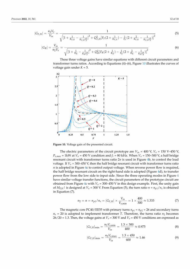
These three voltage gains have similar equations with different circuit parameters andtransformer turns ratios. According to Equations (4)–(6), Figure 10 illustrates the curves ofvoltage gain under K = 5.
Processes 2022, 10, x FOR PEER REVIEW 12 of 19
eor
r
eo
eor
rnmr
r
eor
rnm
in
o
fbc
fdeHF
RnsC
Lsn
R
RnsC
LsnsLsC
sL
RnsC
LsnsL
VVn
VVn
sG
,222
222
,
,222
222_1,
1,11,1
,222
222_1,
2
,
,2,
/1
/1//1
/1//
)(
2
2
++×
++++
++
=
==
(2)
einr
r
ein
einr
rmr
r
einr
rm
o
in
fde
fbcR
RCsn
nsL
R
RCsn
nsLsLsC
sL
RCsn
nsLsL
VnV
VnV
sG
,1,1
22
221,1
,
,1,1
22
221,12,
22
,1,1
22
221,12,
2,
2,
1/1///1
1///
/)(
++×
++++
++
=
==
(3)
where GF,L(s), GF,H(s), and GR(s) are the transfer functions of Figure 4b–d, respectively. To further simplify the transfer function Equations in (1)–(3), the circuit parameters are de-fined as Cr1,1 = Cr1,2 = Cr2/n2, Lr1,1 = Lr1,2 = n2Lr2, eorrLF RCLQ ,1,1,1, //4= ,
eorrF,H RCLQ ,1,1,1 //= einrrR RCLQ ,22 //= , 1,11_1,, 2/ rnmLF LLK = ,
1,12_1,, / rnmHF LLK = , 22, / rmR LLK = and rswRF ffFF /== . Then the voltage gains for the three operating modes are expressed as:
22
,
2,
22
,,
1,
)]122(1)12([]111[
1||
FLFF,LFF,LFLF
FLFLF
in
oLF
FKKFKFQ
FKKVVnG
−+−++−+==
(4)
22
,,,
2,
22
,,
2,
)]122(1)12([]111[
1||
FHFHFFHFFHF
FHFHF
in
oHF
FKKFKFQ
FKKV
VnG−+−++−+
== (5)
22
222
2 )]122(1)12([]111[
1||
RRRRRRR
FRR
o
inR
FKKFKFQ
FKKVn
VG−+−++−+
== (6)
These three voltage gains have similar equations with different circuit parameters and transformer turns ratios. According to Equations (4)–(6), Figure 10 illustrates the curves of voltage gain under K = 5.
F
Q = 0
Q = 0.2
Q = 0.3
Q = 0.4
Q = 0.5
Q = 1Q = 2
0 0.25 0.5 0.75 1 1.25 1.50
0.5
1
1.5
2
2.5
3|G|
K = 5
Figure 10. Voltage gain of the presented circuit.
The electric parameters of the circuit prototype are Vin = 400 V, Vo = 150 V–450 V,Po,max = 1kW at Vo = 450 V condition and fr = 80 kHz. When Vo = 150–300 V, a half bridgeresonant circuit with transformer turns ratio 2n is used in Figure 4b, to control the loadvoltage. If Vo = 300–450 V, then the half bridge resonant circuit with transformer turns ration is adopted in Figure 4c to control output voltage. When reverse power flow is required,the half bridge resonant circuit on the right-hand side is adopted (Figure 4d), to transferpower flow from the low side to input side. Since the three operating modes in Figure 4have similar voltage transfer functions, the circuit parameters of the prototype circuit areobtained from Figure 4c with Vo = 300–450 V in this design example. First, the unity gainof MF,H| is designed at Vo = 300 V. From Equation (5), the turn ratio n = np1/ns is obtainedin Equation (7).
n2 = n = np1/ns = |GF,H | ×Vin
Vo,min= 1× 400
300≈ 1.333 (7)
The magnetic core PC40/EE55 with primary turns np1 = np2 = 26 and secondary turnsns = 20 is adopted to implement transformer T. Therefore, the turns ratio n2 becomes26/20 = 1.3. Then, the voltage gains at Vo = 300 V and Vo = 450 V conditions are expressed as
|GF,H |min =n2Vo,min
Vin=
1.3× 300400
≈ 0.975 (8)
|GF,H |max =n2Vo,max
Vin=
1.3× 450400
≈ 1.46 (9)
Processes 2022, 10, 561 13 of 18
Similarly, the voltage gains at Vo = 150 V and Vo = 300 V conditions under low voltageoutput range operation in Figure 4b are expressed as.
|GF,L|min =n1Vo,min
Vin=
2× 1.3× 150400
≈ 0.975 (10)
|GF,L|max =n1Vo,max
Vin=
2× 1.3× 300400
≈ 1.95 (11)
To obtain a voltage gain of more than 1.95 at Vo = 300 V under low voltage output range(|GF,L|max ≈ 1.95), the quality factors Q = 0.2 and K = 5 are selected. For forward powerflow and high voltage output range (300–450 V), the quality factor QF,H =
√Lr1,1/Cr,1/Ro,e
and the inductor ratio KF,H = Lm,1_n2/Lr1,1. The resistance Ro,e at full load is calculated as:
Ro,e =2n2
2
π2 Ro =2× 1.32
3.141592 ×4502
1000≈ 69 Ω (12)
Then, the resonant components can be calculated as:
Lr1,1 = Lr1,2 = QF,H Ro,e/(2π fr) = 0.2× 69/(2× 3.14159× 80000) ≈ 27.45 µH (13)
Lr2 = Lr1,1/n22 = 27.45/1.32 ≈ 16.24 µH (14)
Lm,1 = KF,H Lr1,1 = 5× 27.45 ≈ 137.25 µH (15)
Cr1,1 = Cr1,2 = 1/(2πQF,H frRo,e) = 1/(2× 3.14159× 0.2× 80000× 69) ≈ 144 nF (16)
Cr2 = n22Cr1,1 = 1.32 × 144 ≈ 243 nF (17)
Table 2 shows the circuit components in the laboratory prototype.
Table 2. Circuit components in the laboratory prototype.
Items Parameter
C1, C2 660 µFC3, C4 660 µF
Cr1,1, Cr1,2 144 nFCr2 243 nF
Lr1,1, Lr1,2 27.45 µHLr2 16.24 µHLm,1 137.25 µH
S1–S6 GP50B60PD1 (600 V/33 A)Q 6R125P6 (650 V/19 A)
Transformer np1:np2:ns 26:26:20
4. Experimental Verifications
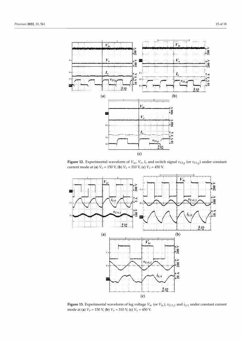
The output voltage Vo between 150 V and 450 V and the switching signals of switchesQ, S1, and S3 are provided in Figure 11a. If Vo is between 150 V and 300 V, S1 is off and Q ison. The half bridge circuit with switches S3 and S4, as shown in Figure 4b, is controlled toregulate load voltage. If Vo is between 300 V and 450 V, Q and S3 are off, and switches S1and S2 are operated to control load voltage. The constant voltage (CV) and constant current(CC) modes are used to charge the battery. If the battery voltage is less that 450 V, then thebattery charge current is controlled at CC mode with Io = 2.3 A. If the battery voltage isclose to 450 V, then CV mode with Vo = 450 V is selected to charge the battery. Therefore, theload current Io will be decreased from 2.3 A. In Figures 12–15, the experimental waveformsoperated at constant current mode with Vo = 150 V, 310 V and 450 V are provided, toshow the circuit characteristics under a forward power flow condition. Figure 12a–cshows the measured waveforms of input voltage, load current, load voltage, and switchsignal under Vin = 400 V, Io = 2.3 A, and Vo = 150, 310, and 450 V, respectively, with CC
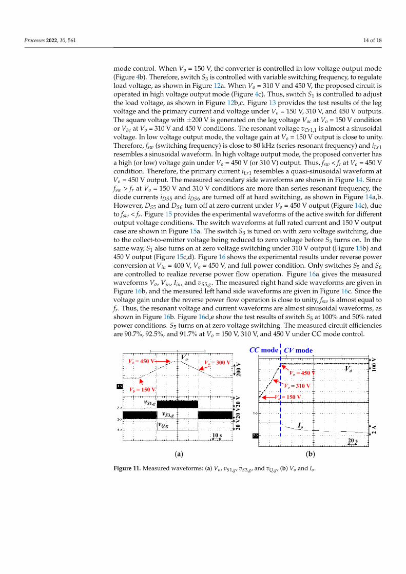
Processes 2022, 10, 561 14 of 18
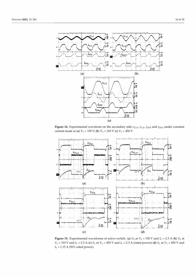
mode control. When Vo = 150 V, the converter is controlled in low voltage output mode(Figure 4b). Therefore, switch S3 is controlled with variable switching frequency, to regulateload voltage, as shown in Figure 12a. When Vo = 310 V and 450 V, the proposed circuit isoperated in high voltage output mode (Figure 4c). Thus, switch S1 is controlled to adjustthe load voltage, as shown in Figure 12b,c. Figure 13 provides the test results of the legvoltage and the primary current and voltage under Vo = 150 V, 310 V, and 450 V outputs.The square voltage with ±200 V is generated on the leg voltage Vac at Vo = 150 V conditionor Vbc at Vo = 310 V and 450 V conditions. The resonant voltage vCr1,1 is almost a sinusoidalvoltage. In low voltage output mode, the voltage gain at Vo = 150 V output is close to unity.Therefore, fsw (switching frequency) is close to 80 kHz (series resonant frequency) and iLr1resembles a sinusoidal waveform. In high voltage output mode, the proposed converter hasa high (or low) voltage gain under Vo = 450 V (or 310 V) output. Thus, fsw < fr at Vo = 450 Vcondition. Therefore, the primary current iLr1 resembles a quasi-sinusoidal waveform atVo = 450 V output. The measured secondary side waveforms are shown in Figure 14. Sincefsw > fr at Vo = 150 V and 310 V conditions are more than series resonant frequency, thediode currents iDS5 and iDS6 are turned off at hard switching, as shown in Figure 14a,b.However, DS5 and DS6 turn off at zero current under Vo = 450 V output (Figure 14c), dueto fsw < fr. Figure 15 provides the experimental waveforms of the active switch for differentoutput voltage conditions. The switch waveforms at full rated current and 150 V outputcase are shown in Figure 15a. The switch S3 is tuned on with zero voltage switching, dueto the collect-to-emitter voltage being reduced to zero voltage before S3 turns on. In thesame way, S1 also turns on at zero voltage switching under 310 V output (Figure 15b) and450 V output (Figure 15c,d). Figure 16 shows the experimental results under reverse powerconversion at Vin = 400 V, Vo = 450 V, and full power condition. Only switches S5 and S6are controlled to realize reverse power flow operation. Figure 16a gives the measuredwaveforms Vo, Vin, Iin, and vS5,g. The measured right hand side waveforms are given inFigure 16b, and the measured left hand side waveforms are given in Figure 16c. Since thevoltage gain under the reverse power flow operation is close to unity, fsw is almost equal tofr. Thus, the resonant voltage and current waveforms are almost sinusoidal waveforms, asshown in Figure 16b. Figure 16d,e show the test results of switch S5 at 100% and 50% ratedpower conditions. S5 turns on at zero voltage switching. The measured circuit efficienciesare 90.7%, 92.5%, and 91.7% at Vo = 150 V, 310 V, and 450 V under CC mode control.
Processes 2022, 10, x FOR PEER REVIEW 15 of 19
and S6 are controlled to realize reverse power flow operation. Figure 16a gives the meas-ured waveforms Vo, Vin, Iin, and vS5,g. The measured right hand side waveforms are given in Figure 16b, and the measured left hand side waveforms are given in Figure 16c. Since the voltage gain under the reverse power flow operation is close to unity, fsw is almost equal to fr. Thus, the resonant voltage and current waveforms are almost sinusoidal wave-forms, as shown in Figure 16b. Figure 16d,e show the test results of switch S5 at 100% and 50% rated power conditions. S5 turns on at zero voltage switching. The measured circuit efficiencies are 90.7%, 92.5%, and 91.7% at Vo = 150 V, 310 V, and 450 V under CC mode control.
vQ,g
Vo
vS1,g
vS3,g
Vo = 300 VVo = 450 V
Vo = 150 V
200
V20
V20
V20
V
10 s
Vo
Io
Vo = 150 V
Vo = 450 V
Vo = 310 V
CC mode CV mode
100
V2
A
20 s
(a) (b)
Figure 11. Measured waveforms: (a) Vo, vS1,g, vS3,g, and vQ,g, (b) Vo and Io.
Vo
Vin
Io
vS3,g
200
V5
A10
0 V
10 V
4 μs
Vo
Vin
Io
vS1,g
200
V5
A20
0 V
10 V
4 μs
(a) (b)
Vo
Vin
Io
vS1,g
500
V5
A50
0 V
10 V
5 μs
(c)
Figure 12. Experimental waveform of Vin, Vo, Io and switch signal vS3,g (or vS1,g) under constant current mode at (a) Vo = 150 V, (b) Vo = 310 V, (c) Vo = 450 V.
Figure 11. Measured waveforms: (a) Vo, vS1,g, vS3,g, and vQ,g, (b) Vo and Io.
Processes 2022, 10, 561 15 of 18
Processes 2022, 10, x FOR PEER REVIEW 15 of 19
and S6 are controlled to realize reverse power flow operation. Figure 16a gives the meas-ured waveforms Vo, Vin, Iin, and vS5,g. The measured right hand side waveforms are given in Figure 16b, and the measured left hand side waveforms are given in Figure 16c. Since the voltage gain under the reverse power flow operation is close to unity, fsw is almost equal to fr. Thus, the resonant voltage and current waveforms are almost sinusoidal wave-forms, as shown in Figure 16b. Figure 16d,e show the test results of switch S5 at 100% and 50% rated power conditions. S5 turns on at zero voltage switching. The measured circuit efficiencies are 90.7%, 92.5%, and 91.7% at Vo = 150 V, 310 V, and 450 V under CC mode control.
vQ,g
Vo
vS1,g
vS3,g
Vo = 300 VVo = 450 V
Vo = 150 V
200
V20
V20
V20
V
10 s
Vo
Io
Vo = 150 V
Vo = 450 V
Vo = 310 V
CC mode CV mode
100
V2
A
20 s
(a) (b)
Figure 11. Measured waveforms: (a) Vo, vS1,g, vS3,g, and vQ,g, (b) Vo and Io.
Vo
Vin
Io
vS3,g
200
V5
A10
0 V
10 V
4 μs
Vo
Vin
Io
vS1,g
200
V5
A20
0 V
10 V
4 μs
(a) (b)
Vo
Vin
Io
vS1,g
500
V5
A50
0 V
10 V
5 μs
(c)
Figure 12. Experimental waveform of Vin, Vo, Io and switch signal vS3,g (or vS1,g) under constant current mode at (a) Vo = 150 V, (b) Vo = 310 V, (c) Vo = 450 V. Figure 12. Experimental waveform of Vin, Vo, Io and switch signal vS3,g (or vS1,g) under constantcurrent mode at (a) Vo = 150 V, (b) Vo = 310 V, (c) Vo = 450 V.
Processes 2022, 10, x FOR PEER REVIEW 16 of 19
Vac
iLr1
vCr1,1
200
V10
0 V
5 A
4 μs
Vbc
iLr1
vCr1,1
200
V10
A10
0 V
4 μs
(a) (b)
Vbc
iLr1
vCr1,1
200
V20
A20
0 V
5 μs
(c)
Figure 13. Experimental waveform of leg voltage Vac (or Vbc), vCr1,1 and iLr1 under constant current mode at (a) Vo = 150 V, (b) Vo = 310 V, (c) Vo = 450 V.
iLr2
vCr2
iDS5
iDS6
100
V10
A10
A10
A
4 μs
iLr2
vCr2
iDS5
iDS6
50 V
10 A
10 A
10 A
4 μs
(a) (b)
iLr2
vCr2
iDS5
iDS6
50 V
10 A
10 A
10 A
5 μs
(c)
Figure 14. Experimental waveform on the secondary side vCr2, iLr2, iDS5 and iDS6 under constant current mode at (a) Vo = 150 V, (b) Vo = 310 V (c) Vo = 450 V.
Figure 13. Experimental waveform of leg voltage Vac (or Vbc), vCr1,1 and iLr1 under constant currentmode at (a) Vo = 150 V, (b) Vo = 310 V, (c) Vo = 450 V.
Processes 2022, 10, 561 16 of 18
Processes 2022, 10, x FOR PEER REVIEW 16 of 19
Vac
iLr1
vCr1,1
200
V10
0 V
5 A
4 μs
Vbc
iLr1
vCr1,1
200
V10
A10
0 V
4 μs
(a) (b)
Vbc
iLr1
vCr1,1
200
V20
A20
0 V
5 μs
(c)
Figure 13. Experimental waveform of leg voltage Vac (or Vbc), vCr1,1 and iLr1 under constant current mode at (a) Vo = 150 V, (b) Vo = 310 V, (c) Vo = 450 V.
iLr2
vCr2
iDS5
iDS6
100
V10
A10
A10
A
4 μs
iLr2
vCr2
iDS5
iDS6
50 V
10 A
10 A
10 A
4 μs
(a) (b)
iLr2
vCr2
iDS5
iDS6
50 V
10 A
10 A
10 A
5 μs
(c)
Figure 14. Experimental waveform on the secondary side vCr2, iLr2, iDS5 and iDS6 under constant current mode at (a) Vo = 150 V, (b) Vo = 310 V (c) Vo = 450 V. Figure 14. Experimental waveform on the secondary side vCr2, iLr2, iDS5 and iDS6 under constantcurrent mode at (a) Vo = 150 V, (b) Vo = 310 V (c) Vo = 450 V.
Processes 2022, 10, x FOR PEER REVIEW 17 of 19
vS3,g
vS3,ce
iS3zvs
10 V
200
V5
A
2 μs
vS1,g
vS1,ce
iS1zvs10
V20
0 V
10 A
2 μs
(a) (b)
vS1,g
vS1,ce
iS1zvs
10 V
200
V10
A
2 μs
vS1,g
vS1,ce
iS1zvs
10 V
200
V10
A
2 μs
(c) (d)
Figure 15. Experimental waveforms of active switch: (a) S3 at Vo = 150 V and Io = 2.3 A (b) S1 at Vo = 310 V and Io = 2.3 A (c) S1 at Vo = 450 V and Io = 2.3 A (rated power) (d) S1 at Vo = 450 V and Io = 1.15 A (50% rated power).
Vo
Vin
Iin
vS5,g
500
V5
A50
0 V
10 V
4 μs
Vde
iLr2
vCr2
200
V10
A20
0 V
4 μs
(a) (b)
iLr1
vCr1,1
iDS1
iDS2
100
V10
A10
A10
A
4 μs
vS5,g
vS5,ce
iS5zvs
10 V
200
V10
A
2 μs
(c) (d)
Figure 15. Experimental waveforms of active switch: (a) S3 at Vo = 150 V and Io = 2.3 A (b) S1 atVo = 310 V and Io = 2.3 A (c) S1 at Vo = 450 V and Io = 2.3 A (rated power) (d) S1 at Vo = 450 V andIo = 1.15 A (50% rated power).
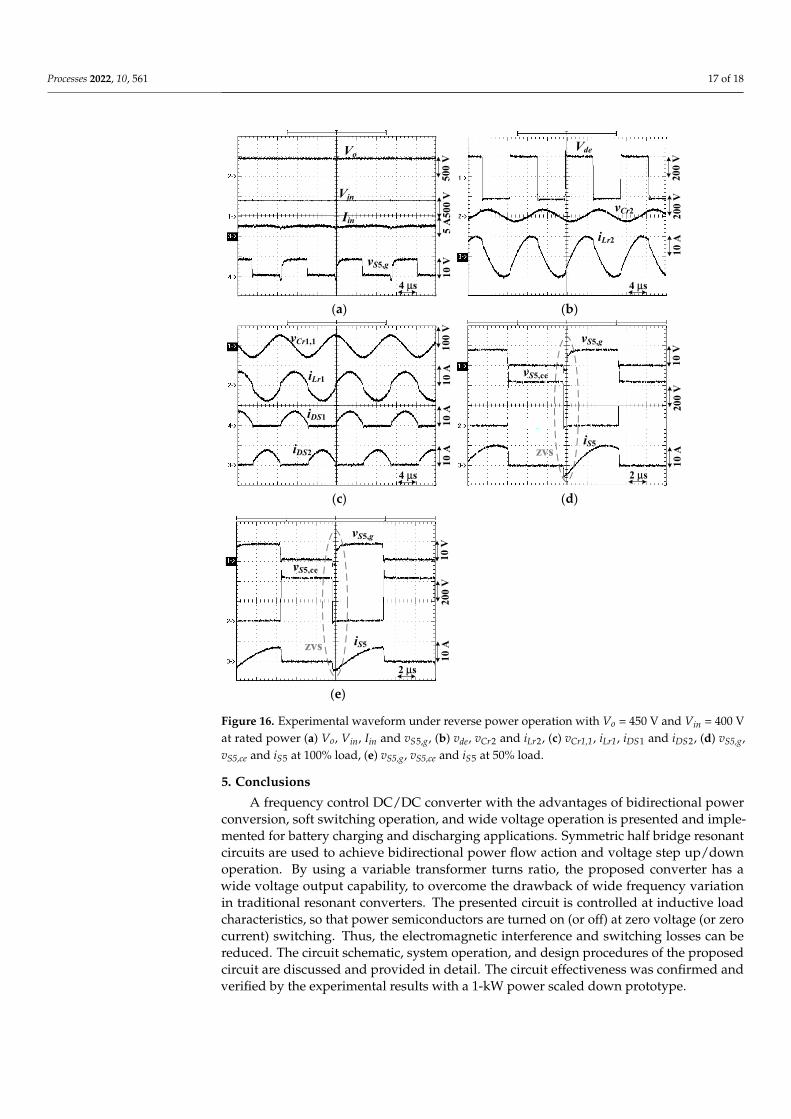
Processes 2022, 10, 561 17 of 18
Processes 2022, 10, x FOR PEER REVIEW 17 of 19
vS3,g
vS3,ce
iS3zvs
10 V
200
V5
A
2 μs
vS1,g
vS1,ce
iS1zvs
10 V
200
V10
A
2 μs
(a) (b)
vS1,g
vS1,ce
iS1zvs
10 V
200
V10
A
2 μs
vS1,g
vS1,ce
iS1zvs
10 V
200
V10
A
2 μs
(c) (d)
Figure 15. Experimental waveforms of active switch: (a) S3 at Vo = 150 V and Io = 2.3 A (b) S1 at Vo = 310 V and Io = 2.3 A (c) S1 at Vo = 450 V and Io = 2.3 A (rated power) (d) S1 at Vo = 450 V and Io = 1.15 A (50% rated power).
Vo
Vin
Iin
vS5,g
500
V5
A50
0 V
10 V
4 μs
Vde
iLr2
vCr2
200
V10
A20
0 V
4 μs
(a) (b)
iLr1
vCr1,1
iDS1
iDS210
0 V
10 A
10 A
10 A
4 μs
vS5,g
vS5,ce
iS5zvs
10 V
200
V10
A
2 μs
(c) (d)
Processes 2022, 10, x FOR PEER REVIEW 18 of 19
vS5,g
vS5,ce
iS5zvs
10 V
200
V10
A
2 μs
(e)
Figure 16. Experimental waveform under reverse power operation with Vo = 450 V and Vin = 400 V at rated power (a) Vo, Vin, Iin and vS5,g, (b) vde, vCr2 and iLr2, (c) vCr1,1, iLr1, iDS1 and iDS2, (d) vS5,g, vS5,ce and iS5 at 100% load, (e) vS5,g, vS5,ce and iS5 at 50% load.
5. Conclusions A frequency control DC/DC converter with the advantages of bidirectional power
conversion, soft switching operation, and wide voltage operation is presented and imple-mented for battery charging and discharging applications. Symmetric half bridge reso-nant circuits are used to achieve bidirectional power flow action and voltage step up/down operation. By using a variable transformer turns ratio, the proposed converter has a wide voltage output capability, to overcome the drawback of wide frequency varia-tion in traditional resonant converters. The presented circuit is controlled at inductive load characteristics, so that power semiconductors are turned on (or off) at zero voltage (or zero current) switching. Thus, the electromagnetic interference and switching losses can be reduced. The circuit schematic, system operation, and design procedures of the pro-posed circuit are discussed and provided in detail. The circuit effectiveness was confirmed and verified by the experimental results with a 1-kW power scaled down prototype.
Funding: This work was supported by the National Yunlin University of Science and Technology, Taiwan, under grant number 109H500311.
Institutional Review Board Statement:
Informed Consent Statement:
Data Availability Statement:
Acknowledgments: The author thanks for the financial support by the NYUST, Taiwan, under grant number 109H500311. The author thanks Y.-C. Liu for his measurement of the experimental wave-forms.
Conflicts of Interest: The author declares no conflict of interest.
References 1. Mao, H.; Lee, C.Y.; Boroyevich, D.; Hiti, S. Review of high-performance three-phase power-factor correction circuits. IEEE Trans.
Ind. Electron. 1997, 44, 437–446. 2. Singh, B.; Singh, B.N.; Chandra, A.; Al-Haddad, K.; Pandey, A.; Kothari, D.P. A review of three-phase improved power quality
AC-DC converters. IEEE Trans. Ind. Electron. 2004, 51, 641–660. 3. Guerrero, J.M.; Loh, P.C.; Lee, T.L.; Chandorkar, M. Advanced control architectures for intelligent microgrids—part II: Power
quality, energy storage, and ac/dc microgrids. IEEE Trans. Ind. Electron. 2013, 60, 1263–1270. 4. Meng, L.; Shafiee, Q.; Trecate, G.F.; Karimi, H.; Fulwani, D.; Lu, X.; Guerrero, J.M. Review on control of DC microgrids and
multiple microgrid clusters. IEEE J. Emerg. Sel. Top. Power Electron. 2017, 5, 928–948. 5. Emadi, A.; Lee, Y.J.; Rajashekara, K. Power electronics and motor drives in electric, hybrid electric, and plug-in hybrid electric vehicles.
IEEE Trans. Ind. Electron. 2008, 55, 2237–2245. 6. Ahrabi, R.R.; Ardi, H.; Elmi, M.; Ajami, A. A novel step-up multi input dc-dc converter for hybrid electric vehicles application.
IEEE Trans. Power Electron. 2017, 32, 3549–3561. 7. Blaabjerg, F.; Dragicevic, T.; Davari, P. Applications of Power Electronics. Electronics 2019, 8, 465.
Figure 16. Experimental waveform under reverse power operation with Vo = 450 V and Vin = 400 Vat rated power (a) Vo, Vin, Iin and vS5,g, (b) vde, vCr2 and iLr2, (c) vCr1,1, iLr1, iDS1 and iDS2, (d) vS5,g,vS5,ce and iS5 at 100% load, (e) vS5,g, vS5,ce and iS5 at 50% load.
5. Conclusions
A frequency control DC/DC converter with the advantages of bidirectional powerconversion, soft switching operation, and wide voltage operation is presented and imple-mented for battery charging and discharging applications. Symmetric half bridge resonantcircuits are used to achieve bidirectional power flow action and voltage step up/downoperation. By using a variable transformer turns ratio, the proposed converter has awide voltage output capability, to overcome the drawback of wide frequency variationin traditional resonant converters. The presented circuit is controlled at inductive loadcharacteristics, so that power semiconductors are turned on (or off) at zero voltage (or zerocurrent) switching. Thus, the electromagnetic interference and switching losses can bereduced. The circuit schematic, system operation, and design procedures of the proposedcircuit are discussed and provided in detail. The circuit effectiveness was confirmed andverified by the experimental results with a 1-kW power scaled down prototype.

Processes 2022, 10, 561 18 of 18
Funding: This work was supported by the National Yunlin University of Science and Technology,Taiwan, under grant number 109H500311.
Acknowledgments: The author thanks for the financial support by the NYUST, Taiwan, under grantnumber 109H500311. The author thanks Y.-C. Liu for his measurement of the experimental waveforms.
Conflicts of Interest: The author declares no conflict of interest.
References1. Mao, H.; Lee, C.Y.; Boroyevich, D.; Hiti, S. Review of high-performance three-phase power-factor correction circuits.
IEEE Trans. Ind. Electron. 1997, 44, 437–446.2. Singh, B.; Singh, B.N.; Chandra, A.; Al-Haddad, K.; Pandey, A.; Kothari, D.P. A review of three-phase improved power quality
AC-DC converters. IEEE Trans. Ind. Electron. 2004, 51, 641–660. [CrossRef]3. Guerrero, J.M.; Loh, P.C.; Lee, T.L.; Chandorkar, M. Advanced control architectures for intelligent microgrids—part II: Power
quality, energy storage, and ac/dc microgrids. IEEE Trans. Ind. Electron. 2013, 60, 1263–1270. [CrossRef]4. Meng, L.; Shafiee, Q.; Trecate, G.F.; Karimi, H.; Fulwani, D.; Lu, X.; Guerrero, J.M. Review on control of DC microgrids and
multiple microgrid clusters. IEEE J. Emerg. Sel. Top. Power Electron. 2017, 5, 928–948.5. Emadi, A.; Lee, Y.J.; Rajashekara, K. Power electronics and motor drives in electric, hybrid electric, and plug-in hybrid electric
vehicles. IEEE Trans. Ind. Electron. 2008, 55, 2237–2245. [CrossRef]6. Ahrabi, R.R.; Ardi, H.; Elmi, M.; Ajami, A. A novel step-up multi input dc-dc converter for hybrid electric vehicles application.
IEEE Trans. Power Electron. 2017, 32, 3549–3561. [CrossRef]7. Blaabjerg, F.; Dragicevic, T.; Davari, P. Applications of Power Electronics. Electronics 2019, 8, 465. [CrossRef]8. Mangu, B.; Akshatha, S.; Suryanarayana, D.; Fernandes, B.G. Grid-connected PV-wind-battery-based multi-input transformer-
couple bidirectional dc-dc converter for household applications. IEEE J. Emerg. Sel. Top. Power Electron. 2016, 4, 1086–1095.[CrossRef]
9. Xu, D.; Zhao, C.; Fan, H. A PWM plus phase-shift control bidirectional DC-DC converter. IEEE Trans. Ind. Electron. 2004,19, 666–675. [CrossRef]
10. Zhao, B.; Song, Q.; Liu, W.; Sun, Y. Overview of dual-active-bridge isolated bidirectional DC–DC converter for high-frequency-linkpower-conversion system. IEEE Trans. Power Electron. 2014, 29, 4091–4106. [CrossRef]
11. Rico, S.J.; Pagano, D.J.; Lucas, K.E. Bidirectional power sharing for DC microgrid enabled by dual active bridge DC-DC converter.Energies 2021, 14, 404. [CrossRef]
12. Jung, J.H.; Kim, H.S.; Ryu, M.H.; Baek, J.W. Design methodology of bidirectional CLLC resonant converter for high-frequencyisolation of DC distribution systems. IEEE Trans. Power Electron. 2013, 28, 1741–1755. [CrossRef]
13. Liu, Y.; Du, G.; Wang, X.; Lei, Y. Analysis and Design of High-Efficiency Bidirectional GaN-Based CLLC Resonant Converter.Energies 2019, 12, 2859. [CrossRef]
14. Zou, S.; Lu, J.; Mallik, A.; Khaligh, A. Bi-directional CLLC converter with synchronous rectification for plug-in electric vehicles.IEEE Trans. Ind. Appl. 2018, 54, 998–1005. [CrossRef]
15. Lin, B.R. Analysis of a series-parallel resonant converter for DC microgrid applications. Processes 2021, 9, 542. [CrossRef]16. Lin, B.R. Analysis and implementation of a frequency control DC-DC converter for light electric vehicle applications. Electronics
2021, 10, 1623. [CrossRef]17. Lin, B.B.; Chen, K.Y. Hybrid LLC Converter with Wide Range of Zero-Voltage Switching and Wide Input Voltage Operation.
Appl. Sci. 2020, 10, 8250. [CrossRef]18. Wang, P.; Zhou, L.; Zhang, Y.; Li, J.; Sumner, M. Input-parallel output-series DC-DC boost converter with a wide input voltage
range, for fuel cell vehicles. IEEE Trans. Veh. Technol. 2017, 66, 7771–7781. [CrossRef]19. Hu, H.; Fang, X.; Chen, F.; Shen, Z.J.; Batarseh, I. A modified high-efficiency LLC converter with two transformers for wide
input-voltage range applications. IEEE Trans. Power Electron. 2013, 28, 1946–1960. [CrossRef]20. Steigerwald, R.L. A Comparison of Half-Bridge Resonant Converter Topologies. IEEE Trans. Power Electron. 1988, 3, 174–182.
[CrossRef]


