Embed Size (px)
Citation preview

DOI: 10.1002/adfm.200500420
Charge Transport and Photocurrent Generation inPoly(3-hexylthiophene):Methanofullerene Bulk-HeterojunctionSolar Cells**
By Valentin D. Mihailetchi, Hangxing Xie, Bert de Boer, L. Jan Anton Koster, and Paul W. M. Blom*
1. Introduction
Organic photovoltaic devices prepared from composite filmsof functionalized fullerenes as electron acceptors (A) and con-jugated polymers as electron donors (D) have recently evolvedas promising cost-effective alternatives to conventional inor-ganic solar cells.[1–3] Unlike inorganic solar cells, photon ab-sorption in bulk-heterojunction (BHJ) D/A organic cellsmainly creates excited electron–hole pairs (excitons) that sub-sequently dissociate at a heterojunction interface via an ultra-fast charge transfer (≈45 fs) from the exited donor to the ac-ceptor.[4] After dissociation, a geminate pair of a hole at thedonor and an electron at the acceptor is formed across the in-terface, which further needs to be separated into free chargecarriers through the assistance of an electric field. These photo-
generated free holes and electrons are then transportedthrough the donor and acceptor phases towards the electrodes,resulting in an external photocurrent density (Jph). As a result,the external photocurrent does not solely depend on the photo-generation rate of free electrons and holes, but also on thetransport properties of the electrons and holes in the acceptorand donor, respectively. Most of the previous work on thephysics of BHJ solar cells was performed on blends ofpoly(2-methoxy-5-(31′,7′-dimethyloctyloxy)-p-phenylene vinyl-ene) (MDMO-PPV) and soluble fullerene derivatives such as[6,6]-phenyl C61-butyric acid methyl ester (PCBM). The powerconversion efficiencies (gs) reported for this type of devices,measured under AM 1.5 (air mass 1.5) standard test condi-tions,[5] range from 2.5 to 3 %.[6,7] However, to achieve theseefficiencies, up to 80 wt.-% of PCBM, a material which barelycontributes to the absorption, has to be added into theMDMO-PPV:PCBM mixture. Recently, we demonstrated thatone of the main reasons for this relatively large amount ofPCBM being required is the enhancement of the hole transportin MDMO-PPV, which is the slowest carrier, when blendedwith PCBM.[8] Furthermore, a too-low hole mobility will alsolead to a buildup of space-charge in the solar cell, which is det-rimental to the fill factor and efficiency.[9] Therefore, an intrin-sically higher hole mobility in the blend permits one to reducethe amount of PCBM and inhibits the occurrence of space-charge, which will further increase the magnitude of the photo-generated current and enhance the g.
Among the materials investigated so far, regioregularpoly(3-hexylthiophene) (P3HT) has demonstrated promising
Adv. Funct. Mater. 2006, 16, 699–708 © 2006 WILEY-VCH Verlag GmbH & Co. KGaA, Weinheim 699
–[*] Prof. P. W. M. Blom, V. D. Mihailetchi, H. X. Xie, Dr. B. de Boer,
L. J. A. KosterMaterials Science Centre, University of GroningenNijenborgh 4, NL-9747 AG Groningen (The Netherlands)E-mail: [email protected]. J. A. KosterDutch Polymer Institute, University of GroningenNijenborgh 4, NL-9747 AG Groningen (The Netherlands)
[**] The authors are indebted to J. C. Hummelen for fruitful discussionsand the generous supply of PCBM, and Minte Mulder for technicalassistance. The work of L. J. A. Koster forms part of the research pro-gram of the Dutch Polymer Institute (#323).
The effect of controlled thermal annealing on charge transport and photogeneration in bulk-heterojunction solar cells madefrom blend films of regioregular poly(3-hexylthiophene) (P3HT) and methanofullerene (PCBM) has been studied. Withrespect to the charge transport, it is demonstrated that the electron mobility dominates the transport of the cell, varying from10–8 m2 V–1 s–1 in as-cast devices to ≈3 × 10⁻⁷ m2 V–1 s–1 after thermal annealing. The hole mobility in the P3HT phase of theblend is dramatically affected by thermal annealing. It increases by more than three orders of magnitude, to reach a value of upto ≈ 2 × 10⁻⁸ m2 V–1 s–1 after the annealing process, as a result of an improved crystallinity of the film. Moreover, upon annealingthe absorption spectrum of P3HT:PCBM blends undergo a strong red-shift, improving the spectral overlap with solar emission,which results in an increase of more than 60 % in the rate of charge-carrier generation. Subsequently, the experimental electronand hole mobilities are used to study the photocurrent generation in P3HT:PCBM devices as a function of annealingtemperature. The results indicate that the most important factor leading to a strong enhancement of the efficiency, comparedwith non-annealed devices, is the increase of the hole mobility in the P3HT phase of the blend. Furthermore, numerical simula-tions indicate that under short-circuit conditions the dissociation efficiency of bound electron–hole pairs at the donor/acceptorinterface is close to 90 %, which explains the large quantum efficiencies measured in P3HT:PCBM blends.
FULL
PAPER

physical properties, such as environmental stability, reason-ably high hole mobility, and an improved absorption as com-pared with PPV-based devices. Thermal annealing of theP3HT:PCBM-blend devices dramatically improves the externalquantum efficiency and g of these cells.[10–12] It is well knownthat an enhanced degree of crystallinity can be induced in poly-thiophene films by thermal annealing. This controlled crystalli-zation and orientation of polythiophene polymer chains cansignificantly improve the hole mobility. After annealing, energyconversion efficiencies as high as 3.5 % have been report-ed.[12,13] Besides this, a red-shift of the optical absorption ofP3HT inside the blend is observed, providing an improvedoverlap with the solar emission.
Figure 1 shows the experimental Jph of such P3HT:PCBMblends (50:50 wt.-%) in a double-logarithmic plot as a functionof effective applied voltage (V0–V).[14] The curves correspondto different postproduction treatments: as-cast, thermally an-nealed at a temperature where the enhancement in g is maxi-mized (120 °C), and annealed at a lower temperature (70 °C).Thermal annealing was performed on complete devices, i.e.,with the photoactive layer between the electrodes, on the hotplate for a period of four minutes. It appears from Figure 1 thatthe photocurrent shows a strong enhancement after thermalannealing. For the completely annealed device (annealed at120 °C), the short-circuit current (JSC) increases by a factor offive, the fill factor (FF) increases by a factor of two, and theoverall enhancement of g is about one order of magnitude,when compared with the device as cast. This dramatic boost inthe efficiency as a result of thermal treatment of the photoac-tive layer has been suggested to be caused by the burning ofshunts,[12] an increase in hole mobility owing to crystallizationof the polymer, a better morphology, or an improved overlapwith the solar emission resulting from the red-shift of the opticalabsorption.[10–12,15] However, the effect of the thermal-annealingprocess on the solar-cell performance in terms of physical pa-rameters, such as the charge-carrier mobility and photocurrentgeneration efficiency, in these devices has not been quantified.
Recently, we have developed a device model which quantita-tively describes the behavior of PPV:PCBM BHJ solar cells. Wehave shown that the dissociation efficiency of bound electron–hole (e–h) pairs, created after photoinduced electron transfer atthe D/A interface, is an important limiting factor in photovoltaicdevices based on this materials system.[8,16,17] Furthermore, withregard to the charge transport, we demonstrated that the photo-current reaches the fundamental space-charge limit when the dif-ference in electron and hole mobilities exceeds two orders ofmagnitude.[9] Herein, we apply the model to understand the ef-fect of postproduction heat treatment at different temperatureson the performance of composite P3HT:PCBM solar cells, andquantify the parameters that limit the device performance. To an-ticipate the results, the most important factor that leads to anincrease in JSC of up to a factor of five is the enhancement ofthe hole mobility of P3HT in the blend by more than three or-ders of magnitude. For partially annealed devices (annealed attemperatures lower than the optimum), the difference in elec-tron and hole mobility is too large, and we demonstrate thatJph is strongly limited by the buildup of space-charge. This re-gime can be discriminated by the 1/2 power dependence of theJph on voltage (as inferred in Fig. 1 by the curve at 70 °C) andthe 3/4 power dependence on light intensity.[9] In the space-charge limit, the FF is not able to exceed 0.42, being approxi-mately constant when varying light intensity and temperature.At optimum annealing temperature (above 110 °C), the differ-ence in electron and hole mobilities is reduced to, typically, afactor of 20 and, consequently, the space-charge no longer lim-its the performance under normal operating conditions. Here,the Jph scales linear with light intensity, and the FF reaches val-ues of 0.7. Furthermore, numerical simulation indicates that atshort-circuit the dissociation efficiency of e–h pairs at the D/Ainterface is close to 90 %, which explains the large quantumefficiencies measured in P3HT:PCBM blends. These results arevaluable for the design of new materials and further improve-ment of the performance of organic photovoltaic devices.
2. Results and Discussion
2.1. Charge-Carrier Transport in Composite P3HT:PCBM Films
Prior to the investigation of the photocurrent of theP3HT:PCBM blends, knowledge about the hole and electronmobilities is indispensable. Recently, much work has been doneto measure the hole mobility of pristine P3HT using field-effecttransistors (FETs),[18,19] time-of-flight (TOF) photocurrentmeasurements,[20] and space-charge-limited (SCL) current in asandwich structure as solar cells or light-emitting diode config-urations.[21] The measured hole mobility ranges from10–8 m2 V–1 s–1 in TOF and SCL current, up to 10–5 m2 V–1 s–1 inFETs. It should be noted that regioregular P3HT self-organizesinto a crystalline structure and, owing to the p–p stacking direc-tion, the charge (hole) transport is extremely efficient. Since inFET measurements the current travels in the plane of the film(parallel to the substrate), the anisotropy in the polymer-chainorientation contributes strongly to the difference in the mea-
700 www.afm-journal.de © 2006 WILEY-VCH Verlag GmbH & Co. KGaA, Weinheim Adv. Funct. Mater. 2006, 16, 699–708
Figure 1. Experimental photocurrent ( Jph) versus effective applied voltage(V0 – V) of the P3HT:PCBM devices at room temperature for as-castdevices and after thermally annealing of the photoactive layers (seelegend). The thickness of the devices (L) is 96 nm and the arrow indicatesthe position of the short-circuit current ( JSC). The dashed lines representthe square-root dependence of the Jph on voltage.
FULL
PAPER
V. D. Mihailetchi et al./Bulk-Heterojunction Solar Cells

sured mobility. Moreover, a different molecular weight ofP3HT, the presence of PCBM, and/or the applcation of a ther-mal treatment will also affect the measured electron and holemobilities.[19,21] Therefore, the relevant values for charge-car-rier mobilities can only be obtained when measured in thesame configuration and experimental conditions as used in anoperational solar-cell device.
Previously, we have shown that electron and hole mobilitiesin the blend can be determined from current–voltage measure-ments by using electrodes that either suppress the injection ofelectrons or holes, resulting in hole- or electron-only devices,respectively.[8,22] In this section, we have applied this techniqueto measure either the hole or electron current in blends ofP3HT:PCBM as a function of the annealing temperature of thespin-coated films. To fabricate the hole-only devices, palladiumwas evaporated as the top electrode in an indium tin oxide(ITO)/poly(3,4-ethylenedioxythiophene):poly(4-styrene sulfo-nate) (PEDOT:PSS)/P3HT:PCBM structure. The work func-tion of PEDOT:PSS matches the highest occupied molecularorbital (HOMO) of P3HT at 4.9 eV, forming an Ohmic contactfor hole injection,[11,21] whereas palladium strongly suppresseselectron injection into PCBM owing to the large mismatch be-tween its work function and lowest unoccupied molecular or-bital (LUMO) of PCBM.[23] A schematic diagram of a hole-only device is shown in the inset of Figure 1a. In order to sup-press the hole injection into P3HT, the bottom contact musthave a low work function. Recently, we demonstrated that thework function of a noble metal (such as silver) can be modifiedusing a self-assembled monolayer (SAM).[24] This techniqueworks very well and successful electron-only devices were con-structed using blends of MDMO-PPV:PCBM.[8] Therefore, simi-lar electron-only devices were also constructed for theP3HT:PCBM blends, the schematic band diagram of such anelectron-only device is presented as an inset in Figure 2b.
Figure 2 shows the experimental dark-current densities (JD)of P3HT:PCBM blends that were measured in hole-only(Fig. 2a) and electron-only (Fig. 2b) devices for different an-nealing temperature performed on the completed device. Forclarity, only the devices that were measured as cast, and afterthermal annealing at 90 °C and 120 °C, are shown. The appliedvoltage was corrected for the built-in voltage (VBI) and thevoltage drop (VRS) arising from the substrate’s series resis-tance.[25] When the applied voltage is greater that VBI, JD
throughout all devices scales quadratically with voltage, indica-tive of SCL transport. This observation is common for low-mobility, disordered semiconductors and it allows for a directdetermination of the mobility.[8,21,22] For the electron- and hole-only devices the SCL current is approximated by[26]
Je�h� �98
�0 �r le�h�exp 0�891ce�h�
����VL
�� �V2
L3 (1)
where Je(h) is the electron (hole) current, le(h) the zero-fieldmobility of the electrons (holes), ce(h) the field activationfactor, e0 the permittivity of free space, er the relative permittiv-ity of the material, and L the thickness of the active layer. Theexperimental data in Figure 2 were fitted using Equation 1,and the results are shown by the solid lines.
Figure 3 shows the calculated zero-field mobility of electronsand holes in 50:50 wt.-% blends of P3HT:PCBM devices as afunction of the annealing temperature. For comparison, the holemobility of pristine P3HT, measured under the same experi-
Adv. Funct. Mater. 2006, 16, 699–708 © 2006 WILEY-VCH Verlag GmbH & Co. KGaA, Weinheim www.afm-journal.de 701
Figure 2. Experimental dark-current densities ( JDs) of the 50:50 wt.-%P3HT:PCBM-blend devices measured at room temperature in the hole-only (a) and electron-only (b) device configuration, as shown by the insetschematic diagrams. The symbols correspond to different annealing tem-peratures of the photoactive layer as follow: as-cast (�), 90 °C (�), and120 °C (�), respectively. Here, the thickness of the annealed hole-only de-vices (�,�) is 120 nm, whereas for the other devices is 220 nm. The solidlines represent the fit using a model of single-carrier SCL current withfield-dependent mobility (Eq. 1). The JD–V characteristics are corrected forthe voltage drop over the contacts (VRS) and the built-in voltage (VBI) thatarises from the work-function difference between the contacts.
Figure 3. Room-temperature electron (�) and hole (�) zero-field mobili-ties in 50:50 wt.-% blends of P3HT:PCBM as a function of postproductionannealing temperature of the completed devices. For comparison, the holemobility measured in pristine P3HT devices (�) is also shown. The mobil-ities were calculated from the SCL current measured using the electron-and hole-only device configuration (Fig. 2).
FULL
PAPER
V. D. Mihailetchi et al./Bulk-Heterojunction Solar Cells
mental conditions, is also shown. It appears from Figure 3 thatthe hole mobility in pristine P3HT is hardly affected by thermalannealing, with a typical value of (1.4–3.0) × 10–8 m2 V–1 s–1. Thismobility was found to be completely field-independent (ch = 0)and fully consistent with previously reported values for high-mo-lecular-weight P3HT (such as the one used here).[21] In contrast,the hole mobility of P3HT in the blend is strongly affected by thepresence of PCBM and it drops almost four orders of magnitudefor an as-cast device. Upon annealing, however, the mobilitystarts to increase sharply with an onset at 50–60 °C, followed bysaturation to approximately the value of the pristine polymerwhen the devices are annealed above 120 °C. Also, the field acti-vation factor gradually decreases from ch ≈ 4.0 × 10⁻⁴ (V m–1)–1⁄2for the as-cast film to ch = 0 (V m–1)–1⁄2 for the devices annealedabove 90 °C. Moreover, the electron mobility of PCBM in theblend is also affected by thermal annealing: for as-cast films theelectron mobility is (1–2) × 10–8 m2 V–1 s–1, typically a factor of5000 higher than the hole mobility. As a result, the charge trans-port in as-cast films is strongly unbalanced and the current is fullydominated by the electrons. Interestingly, for the same volumefraction the electron mobility in as-cast P3HT:PCBM films re-sembles the value measured previously in MDMO-PPV:PCBMblends.[8] However, thermal annealing of P3HT:PCBM films re-sults in an electron mobility enhanced by, typically, a factor of 30,with an onset corresponding to the same temperature observedfor the hole mobility, as inferred from Figure 3.
Furthermore, modulated differential scanning calorimetry(DSC) has been used to assess the degree of crystallinity of theparticular batch of regioregular P3HT used in these experi-ments. The DSC thermogram, measured using a scan rate of2 K min–1, reveals two weak changes in the gradient at ≈50 °C,which correspond to the onset of the side-chain melting tem-perature (Tsc), and at ≈125 °C, corresponding to the onset ofthe glass-transition temperature (Tg); Furthermore, a strongmelting peak appears at ≈215 °C. These results are valuable forunderstanding the film-formation mechanism and the chargetransport in these blends. It has been shown that regioregularP3HT self-organizes into microcrystalline lamellae structure,forming well-defined whiskerlike entities.[27–29] This predomi-nantly crystalline film may already have been formed in thepristine P3HT directly after the spin-coating process and ther-mal annealing does not further improve the crystallinity. As aconsequence, the hole mobility in the pristine P3HT is notexpected to change after the annealing of the film. However, inthe blend devices, the presence of PCBM molecules might pre-vent immediate crystallization of P3HT after the spin-coatingprocess, resulting in a more amorphous film. This hypothesis isstrengthened by a recent preposition made by Yang et al. whoargue that a rather homogeneous nanoscale distribution ofPCBM in the P3HT matrix is present in the film as cast.[15]
Consequently, the conformation of the P3HT chains and theway they pack together results in a weak interchain interactionwhich strongly suppresses the hole mobility. Upon thermal an-nealing, slow crystallization of P3HT takes place and demixingbetween P3HT and PCBM is observed,[15] which leads to an en-hanced charge transport. As a result, interpenetrating networkscomposed of P3HT crystals and aggregated nanocrystalline
PCBM-rich domains are formed, which provide continuouspathways in the entire photoactive layer for efficient electronand hole transport. It appears from Figure 3 that the onset inboth electron and hole mobility in P3HT:PCBM blends corre-sponds with Tsc. Above this temperature the side-chain ofP3HT melts, allowing PCBM molecules to diffuse and formnanocrystalline domains of pure PCBM which subsequently re-sult in an enhanced electron transport, as seen experimentally.Moreover, heating above Tg allows the freely formed chains inthe polymer melt to disentangle into a lower-energy conforma-tion. This presumed straightening and crystallization of thepolymer strands upon annealing will lead to a more planar p–pstacking, thereby increasing the interchain interaction and holemobility. In section 2.3, the experimental charge-carrier mobil-ities of Figure 3 will be used to analyze the photocurrent gen-eration and the performance of the solar cells as a function ofannealing temperature.
2.2. Optical Absorption Spectra
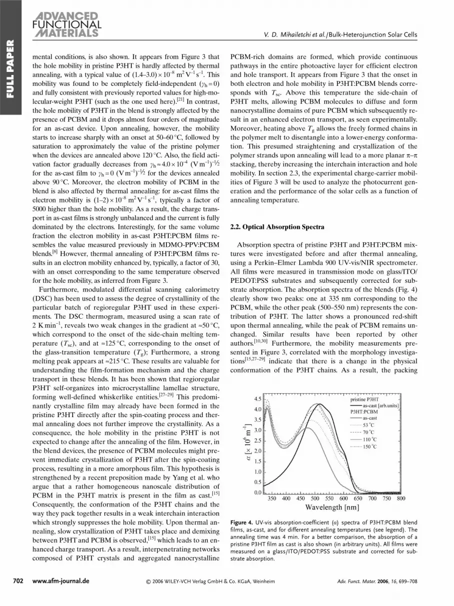
Absorption spectra of pristine P3HT and P3HT:PCBM mix-tures were investigated before and after thermal annealing,using a Perkin–Elmer Lambda 900 UV-vis/NIR spectrometer.All films were measured in transmission mode on glass/ITO/PEDOT:PSS substrates and subsequently corrected for sub-strate absorption. The absorption spectra of the blends (Fig. 4)clearly show two peaks: one at 335 nm corresponding to thePCBM, while the other peak (500–550 nm) represents the con-tribution of P3HT. The latter shows a pronounced red-shiftupon thermal annealing, while the peak of PCBM remains un-changed. Similar results have been reported by otherauthors.[10,30] Furthermore, the mobility measurements pre-sented in Figure 3, correlated with the morphology investiga-tions[15,27–29] indicate that there is a change in the physicalconformation of the P3HT chains. As a result, the packing
702 www.afm-journal.de © 2006 WILEY-VCH Verlag GmbH & Co. KGaA, Weinheim Adv. Funct. Mater. 2006, 16, 699–708
Figure 4. UV-vis absorption-coefficient (a) spectra of P3HT:PCBM blendfilms, as-cast, and for different annealing temperatures (see legend). Theannealing time was 4 min. For a better comparison, the absorption of apristine P3HT film as cast is also shown (in arbitrary units). All films weremeasured on a glass/ITO/PEDOT:PSS substrate and corrected for sub-strate absorption.
FULL
PAPER
V. D. Mihailetchi et al./Bulk-Heterojunction Solar Cells

together of P3HT in the presence of PCBM is different, rela-tive to that in pristine P3HT films, thereby altering the relevantoptical and electronic properties that are critical for the opera-tion of these devices. This change in the conformation is alsoreflected in the absorption spectra of the blend films. As shownin Figure 4, the UV-vis absorption-coefficient spectra of theblend film as cast is strongly blue-shifted with respect to thespectrum of pristine P3HT. This shift might originate from atighter chain coil, produced by twisting of the polymer back-bone or broken conjugation in the presence of PCBM, result-ing in segments with a shorter conjugation length and weakerinterchain interaction. This is consistent with absorption spec-tra of pristine P3HT, which show no change after annealing,but, rather, a small increase in the absorption intensity (notshown). Upon annealing, the PCBM demixes from the P3HT,as inferred by Yang et al.,[15] thereby increasing the degree ofcrystallinity of the polymer and consequently undergoes a no-ticeable shift to the red, approaching the spectrum of the pris-tine polymer. It appears from Figure 4 that the shift of the opti-cal absorption is maximized when the devices are annealedabove 100 °C, which closely corresponds with the temperatureat which the hole mobility in the blend begins to approach thatof the pristine polymer.
Nevertheless, the net effect of the red-shift of the opticalabsorption upon annealing, with respect to the nontreated film,is that it will improve the spectral overlap with solar emission,resulting in an increased absorption in the device. The absorp-tion coefficients (a) shown in Figure 4 can be used to estimatethe amount of additionally absorbed photons upon thermallyannealing the P3HT:PCBM BHJ solar cell. The calculation wasdone using the following equation (as a function of wavelength,k):
Iabs�k� � I0�k���1 � 10�a�k�L� � R�k� � 10�2a�k�L�10�a�k�L�� (2)
where Iabs is the fraction of absorbed photons, I0 the light-source spectrum, and R the reflectivity of the top-electrodematerial (Al; R ≈ 92 % on the involved spectral range).[31] Theresults of the calculations are shown in Figure 5 together withthe light-source spectrum used in our measurements (I0), for a
device with a thickness (L) of 96 nm. After integrating the areaunder the curves it appears that the annealed device improveslight harvesting by approximately 60 % relative to thenontreated device. In the next section this information will beused to explain the enhanced photocurrent generation in theannealed devices.
2.3. Device Characterization under Illumination
2.3.1. The Effect of Thermal Annealing on Solar-CellPerformance
After the investigation of the charge transport and opticalabsorption spectroscopy we proceeded with the analysis ofthe solar-cell performance upon thermal annealing of thephotoactive P3HT:PCBM layer. The devices consisted of50:50 wt.-% P3HT:PCBM blends which were spin-coated froma single chloroform solution on an ITO/PEDOT:PSS substrate,followed by the evaporation of a thin samarium (8 nm)/alumi-num (100 nm) top electrode. The annealing was performed,after completing the devices, in a N2 atmosphere on a hot platefor a duration of four minutes. The active layer thicknessranged from 94 to 97 nm for all fabricated devices.
Figure 6 shows the variation of the principal photovoltaic pa-rameters (i.e., their mean values together with the standard de-viations) as a function of annealing temperature. The deviceswere illuminated from a halogen lamp with the spectral rangeand shape shown in Figure 5, calibrated using a silicon diode at
Adv. Funct. Mater. 2006, 16, 699–708 © 2006 WILEY-VCH Verlag GmbH & Co. KGaA, Weinheim www.afm-journal.de 703
Figure 5. Fraction of absorbed photons (Iabs) from the excitation source(I0) by a P3HT:PCBM solar cell with a thickness of L= 96 nm. The calcula-tion is done for the film as cast and after annealing at 120 °C (see legend)using the absorption coefficients (a) given in Figure 4.
Figure 6. Device performance of the 50:50 wt.-% P3HT:PCBM blends, un-der illumination from a halogen lamp, as a function of annealing tempera-ture. The annealing was done on a hot plate in a N2 atmosphere for4 min. The thickness of all devices (L) ranged from 94 to 97 nm.
FULL
PAPER
V. D. Mihailetchi et al./Bulk-Heterojunction Solar Cells

an intensity of approximately 1.15 Sun (115 mW cm–2). Theopen-circuit voltage (VOC) is relatively constant and varies lessthan 40 mV, showing a slight increase above 150 °C. Conver-sely, all remaining device parameters show a very fast increasewith annealing temperature between 50 and 110 °C, followedby saturation. The onset of this enhancement strongly corre-sponds with the onset in the hole mobility of P3HT in the blend(Fig. 3), and occurs above Tsc. Furthermore, the saturationappearing in JSC, FF, and g when annealed above 110 °C seemsalso to be related to the P3HT hole mobility. Above thisannealing temperature the enhancement of the hole mobilityof P3HT in the blend is maximized, and, consequently, the dif-ference between the electron and hole mobilities is reduced,typically, to a factor of 20, leading to a much more balancedtransport. In particular, the thermal treatment produced a five-fold enhancement of JSC, a twofold increase of FF, and, conse-quently, a tenfold gain of g (as inferred from Fig. 6). It is worthmentioning that the g does not show a clear optimum at a par-ticular annealing temperature, but is, rather, unchanged above110 °C, in contrast with previously reported results.[10–12,15] Wehave identified that the source of the decreasing performancein these studies, when annealing above 130 °C, is the degrada-tion of the LiF/Al top electrode. With a samarium cathode, asused in our study, this problem does not occur. As a further testwe applied a LiF/Al cathode after the thermal-annealing step,and in that case also no decrease in performance was observedat higher annealing temperatures.
To identify the main origin of the performance enhancementas a function of annealing treatment, the effects of enhancedabsorption owing to the absorption red-shift and the increasedcharge transport must be disentangled. With regard to theabsorption, the shaded area in Figure 5 represents the addi-tional fraction of photons absorbed by the film upon annealing.This shaded area is now plotted in Figure 7 in the form of therelative enhancement with respect to the untreated film for allannealing temperatures. Thus, Figure 7 shows that, comparedto the untreated film, the total absorption increases by a factorof 1.6 for films annealed above 100 °C. In a recent study we
showed that at high reverse voltages the photocurrent isfully saturated, being independent of voltage and tempera-ture.[8,17] In this regime the saturated photocurrent is given byJsat = q Gmax L, with q the electric charge and Gmax the maxi-mum generation rate of e–h pairs by the solar-cell device. Inthis saturated regime all bound e–h pairs are separated intofree carriers and consequently Gmax is only governed by theamount of absorbed photons. In Figure 7, the relative increaseof Gmax, determined from the saturated photocurrent at higheffective voltages ((V0 – V) > 10 V) as shown in Figure 1, isplotted. Gmax ranges from 3.56 × 1027 m–3 s–1 for as-cast devicesto 5.7 × 1027 m–3 s–1 for the annealed (120 °C) devices. Figure 7convincingly demonstrates that the increase in Gmax is com-pletely a result of the enhanced absorption, which implies thatall additionally generated excitons in the P3HT phase of theblend are able to dissociate at the D/A interface and form e–hpairs. This is further supported by a recent preposition madeby Yang et al. who showed that the fibrillar-like P3HT crystalsthat form upon annealing at 120 °C do not significantly reducethe interface area with the electron acceptor PCBM.[15] The or-igin of the decrease of Gmax above 130 °C is presently notknown. Thus, as a first step, we have demonstrated that the in-crease of the photocurrent with a factor of 1.6 at high reversevoltages is solely the result of an increase of the optical absorp-tion. However, for comparison, JSC increases by a factor of fiveupon annealing, as shown in Figure 6. Therefore, this strong in-crease, together with the enhancement of the FF, cannot be at-tributed to the absorption increase of the film upon annealing.An important question that remains is what mechanism domi-nates such a strong enhancement in JSC and FF of the cell andwhat limits the performance of an as-cast device or a device an-nealed at lower temperature.
Recently, we have demonstrated that the photocurrent inpolymer/fullerene blends can be limited by the buildup ofspace-charge, even under normal operation conditions (1 Sunillumination). This SCL photocurrent occurs when the differ-ence between electron and hole mobility is too large.[9] Thefingerprints of a SCL photocurrent are its square-root depen-dence on voltage and a 3/4 dependence on light intensity.[9] Themobility measurements presented in Figure 3 show that thereis a greater than two orders of magnitude difference betweenthe electron and hole mobilities in as-cast devices and devicesannealed up to 90 °C. As expected, the photocurrents shown inFigure 1 indeed exhibit a square-root dependence on voltagefor both the as-cast film and the device annealed at 70 °C. Inthe following section, the dependence of the photocurrent onlight intensity of devices annealed at low temperatures isfurther investigated.
2.3.2. Light-Intensity Dependence
To gain further insight in the operation of P3HT:PCBMdevices and quantify the limiting parameters, the light-intensity(Plight) dependence of the photocurrent has been studied forthe device annealed at 70 °C). The Plight was varied from1000 W m–2 (upper curve) down to 76 W m–2 using a set ofneutral density filters with a constant optical density over the
704 www.afm-journal.de © 2006 WILEY-VCH Verlag GmbH & Co. KGaA, Weinheim Adv. Funct. Mater. 2006, 16, 699–708
Figure 7. Relative enhancement [%] of the absorbed photons and maxi-mum generation rate (Gmax) for an annealed compared to an as-cast de-vice, as a function of annealing temperature. The absorption was calcu-lated from the shaded area in Figure 5, whereas Gmax was determinedfrom the saturation of the photocurrent ( Jsat = q Gmax L) at high effectivevoltages (V0 – V) shown in Figure 1.
FULL
PAPER
V. D. Mihailetchi et al./Bulk-Heterojunction Solar Cells

spectral range of the light source (shown in Fig. 5). Subse-quently, the resulting spectrum of each filter-lamp combinationwas recorded and integrated over the absorption spectrum ofthe blend P3HT:PCBM film, which gave the intensity. There-fore, the generation rate (G) of e–h pairs is proportional to thelight intensity (G ∝ Plight). Qualitatively, Jph follows the power-law dependence:
Jph ∝ PSlight (3)
where the exponent S ranges from 0.75 in the case of SCLphotocurrent to 1.0 for the space-charge-free limit.[9]
Figure 8 shows the Jph–(V0 – V) characteristics of theP3HT:PCBM device, after thermal annealing at 70 °C as shownin Figure 1, as a function of Plight. It is observed that for(V0 – V) < 0.03 V, the Jph shows linear dependence on voltageat all light intensities, which is caused by the opposite effects ofdrift and diffusion of charge carriers.[9,16,17] Above 0.03 V, how-ever, a square-root dependence on voltage of the experimentalJph is observed, as is predicted for blends with a large differ-ence in electron and hole mobilities.[9] At even larger voltagesthe Jph shows a clear transition to the saturation regime whereit becomes limited by the field (E) and temperature (T)dependence of the dissociation of bound e–h pairs;Jph = q G(E,T) L.[17] These results are distinctly different whenthe devices are annealed at higher temperature, where the elec-tron and hole transport is more balanced. In that case, no square-root dependence of Jph is observed, as seen in Figure 1 in thecurve at 120 °C. Moreover, it appears from Figure 8 that Jph
shows weaker Plight dependence in the square-root regime com-pared to the saturation regime. Figure 9 displays, on a double-logarithmic scale, the experimental Jph taken from Figure 8 asa function of light intensity for two different voltages; at(V0 – V) = 0.1 V in the square-root regime and at (V0 – V) = 3 Vin the saturation regime. The slope S determined from the line-ar fit (lines) to the experimental data (as shown in Fig. 9)clearly proves that Jph is limited by the buildup of space-chargein the square-root regime and becomes space-charge-free inthe saturation regime.[9] Because the JSC (indicated by the ar-
row in Fig. 8) at high light intensity falls in the square-root partof the Jph–(V0 – V) characteristics, the device is fully limited bythe buildup of space-charge between the open- and short-cir-cuit points. In this case the FF of the device is reduced to lessthan 0.42 and the JSC approaches a 3/4 Plight dependence(S ≈ 0.75). By decreasing the light intensity, the transition volt-age from square-root to saturation moves to lower values andthe device is only partially limited by the space-charge.[9] As aconsequence, the FF of the device increases and the JSC ap-proaches a linear dependence on light intensity (S ≈ 1).
From Figure 8 it is clear that the buildup of space-chargedramatically reduces the device performance, since it causes afundamental limitation on FF and JSC. This space-charge is adirect result of the unbalanced transport of electrons and holesin the device. Owing to the strongly increased hole mobility,leading to a better balanced transport, this limitation is pre-vented under normal operating conditions in the device an-nealed above 110 °C. The absence of space-charge effects isfurther evidenced by a completely linear (S = 1.0) dependenceof Jph on Plight (data not shown). Thus, the enhancement in thedevice efficiency by a factor of ten upon thermal annealing ismainly a result of the improved hole mobility of P3HT insidethe blend by more than three orders of magnitude, rather thanby improving light harvesting (with ≈60 %). With increasedhole transport, the devices recover from the space-charge lim-itation to become space-charge-free, as a result of a more bal-anced transport. As shown in Figure 1, the absence of thesquare-root voltage dependence in the device annealed at110 °C leads to a strong enhancement of both FF and JSC. Inorder to fully quantify the device performance we have ana-lyzed the photocurrent generation in P3HT:PCBM solar cellsfurther, with the help of numerical simulations.[16]
2.3.3. Numerical-Simulation Results
Recently, we have shown that the photocurrent in conjugat-ed polymer/fullerene blends is dominated by the dissociationprobability [P(E,T)] of e–h pairs at D/A interface, which is afield- and temperature-dependent process.[17] In the saturation
Adv. Funct. Mater. 2006, 16, 699–708 © 2006 WILEY-VCH Verlag GmbH & Co. KGaA, Weinheim www.afm-journal.de 705
Figure 8. Light-intensity dependence of the photocurrent ( Jph) versus ef-fective applied voltage (V0 – V) of the device thermally annealed at 70 °C.The intensity was varied from 1000 (upper curve) down to 76 W m–2,whereas the arrow indicats the position of the short-circuit current ( JSC).
Figure 9. Light-intensity dependence of the photocurrent ( Jph) taken fromFigure 8 at an effective voltage of (V0 – V) = 0.1 V and (V0 – V) = 3.0 V (sym-bols). The slope (S) determined from the linear fit (solid lines) to theexperimental data is written on the figure.
FULL
PAPER
V. D. Mihailetchi et al./Bulk-Heterojunction Solar Cells
regime the photocurrent is given by Jph = q G(E,T) L, whereG(E,T) = P(E,T) Gmax. The probability P depends on the initiale–h separation distance (a) and the decay rate of bound pair(kF). Once separated, the free electron and hole can again bi-molecularly recombine at the interface to form a bound pairwith a rate constant (kR),[32] which may dissociate again duringits lifetime. To fit the experimental data, the G(E,T) has beentaken into account in a numerical model which solves the stea-dy-state continuity equations for electrons and holes includingdiffusion, recombination, and space-charge effects via the Pois-son equation.[16] For MDMO-PPV:PCBM-blend devices, thismodel quantitatively explained the behavior of the photocur-rent as a function of temperature and PCBM composi-tion.[8,16,17] The most limiting factor in these blends is the disso-ciation efficiency of bound e–h pairs across the D/A interface,which is only 60 % at room temperature under short-circuitconditions. To calculate the photocurrent for the P3HT:PCBMdevices, the input parameters required in the model are: thecharge-carrier mobilities of electrons and holes, the spatiallyaveraged dielectric constant (er) of P3HT and PCBM, the ini-tial (e–h) separation distance (a), the bound-pair lifetime (kF
–
1), the maximum generation rate (Gmax), and the semiconduc-tor bandgap (Eg). Since er for P3HT and PCBM are know, theEg is estimated from the HOMO(P3HT)–LUMO(PCBM) dif-ference, Gmax is determined from the saturation of the photo-current (Fig. 7), and the charge-carrier mobilities are presentedin Figure 3; the only adjustable parameters of the model thatremain are a and kF
–1. Similarly to MDMO-PPV:PCBM blends,a and kF can be independently determined from the field-de-pendent dissociation probability P(E,T) by fitting the tempera-ture dependence of the photocurrent.[17] Under sufficient ap-plied reverse bias (≤ –3 V), all e–h pairs are dissociated and theJph approaches full saturation, being field- and temperature-in-dependent. This saturation allows determination of a. Subse-quently, kF is determined by fitting the field dependence of theJph.
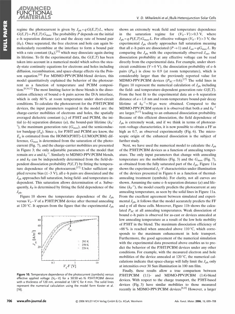
Figure 10 shows the temperature dependence of the Jph
versus V0 – V of a P3HT:PCBM device after thermal annealingat 120 °C. It appears from the figure that the experimental Jph
shows an extremely weak field and temperature dependencein the saturation regime for (V0 – V) > 0.3 V, whereJph = q P(E,T) Gmax L. For effective voltages (V0 – V) > 3 V, theexperimental Jph clearly approaches full saturation meaningthat all e–h pairs are dissociated (P → 1) and Jsat = qGmax L. Bycomparing the Jph with the experimentally observed Jsat, thedissociation probability at any effective voltage can be readdirectly from the experimental data. For example, under short-circuit conditions (V = 0 V), the dissociation probability of e–hpairs (PSC) is close to 0.9 (at room temperature), which isconsiderably larger than the previously reported value forMDMO-PPV:PCBM devices (PSC = 0.6).[17] The solid lines inFigure 10 represent the numerical calculation of Jph includingthe field- and temperature-dependent generation rate G(E,T).From the best fit to the experimental data an e–h separationdistance of a = 1.8 nm and room-temperature bound-pair decaylifetime of kF
–1 ≈ 50 ls were obtained. Compared to theMDMO-PPV:PCBM system it is observed that both a and kF
–1
are larger,[8,17] leading to an enhanced dissociation probability.Because of this efficient dissociation, the field dependence ofJph is extremely weak, and if we think in terms of photocur-rent–voltage characteristics, it is now possible to obtain a FF ashigh as 0.7, as observed experimentally (Fig. 6). The micro-scopic origin of the enhanced dissociation is the subject offurther study.
Next, we have used the numerical model to calculate the Jph
of the P3HT:PCBM devices as a function of annealing temper-ature. The only input parameters that change with annealingtemperature are the mobilities (Fig. 3) and the Gmax (Fig. 7),as obtained from the fully saturated part of the Jph. Figure 11ashows the experimental JL–V characteristics under illuminationof the devices presented in Figure 6 as a function of thermal-annealing treatment (symbols). For clarity, not all curves areshown. Assuming the same e–h separation distance (a) and life-time (kF
–1), the model exactly predicts the photocurrent at anyannealing temperature, as seen by the solid lines in Figure 11a.From the excellent agreement between simulated and experi-mental Jph, it follows that the model accurately predicts the FFand g of all these cells. Moreover, Figure 11b shows the calcu-lated PSC at all annealing temperatures. Weak dissociation ofbound e–h pairs is observed for as-cast or devices annealed atlow annealing temperature as a result of the low hole mobilityof P3HT in the blend. The maximum dissociation efficiency of≈88 % is reached when annealed above 110 °C, which corre-sponds to the maximum enhancement in hole transport.Furthermore, the good agreement of the numerical simulationwith the experimental data presented above enables us to pre-dict the behavior of the P3HT:PCBM devices under any otherconditions. For example, with the measured electron and holemobilities of the device annealed at 120 °C, the numerical cal-culations indicate that space-charge will fully limit the Jph onlyat intensities over 30 Sun illumination in 100 nm film.
Finally, these results allow a true comparison betweenP3HT:PCBM (1:1)- and MDMO-PPV:PCBM (1:4)-blenddevices. With respect to the charge transport, the P3HT-baseddevices (Fig. 3) have similar mobilities to those measuredrecently in MDMO-PPV:PCBM devices.[8,22] However, a larger
706 www.afm-journal.de © 2006 WILEY-VCH Verlag GmbH & Co. KGaA, Weinheim Adv. Funct. Mater. 2006, 16, 699–708
Figure 10. Temperature dependence of the photocurrent (symbols) versuseffective applied voltage (V0 – V) for a 50:50 wt.-% P3HT:PCBM devicewith a thickness of 120 nm, annealed at 120 °C for 4 min. The solid linesrepresent the numerical calculation using the model form Koster et al.[16].
FULL
PAPER
V. D. Mihailetchi et al./Bulk-Heterojunction Solar Cells

volume fraction of absorbing material (P3HT) combined withmore red-shifted absorption increases the maximum rate ofcharge-carrier generation (Gmax) in 50:50 wt.-% P3HT:PCBMdevices by more than a factor of two, as compared to the20:80 wt.-% MDMO-PPV:PCBM devices.[8] Combining this witha higher separation efficiency of photogenerated bound e–h pairsunder short-circuit conditions increases the JSC by more than afactor two for the P3HT-based devices. Also, the FF of theP3HT:PCBM solar cells is larger with respect to the values mea-sured in MDMO:PCBM devices, as a result of a weaker fielddependence of the photocurrent. The most limiting factor of allP3HT-based devices remains, however, the VOC, which is ap-proximately 40 % lower as compared to that of the MDMO-based devices. However, the increase in current and FF makeup for the loss in VOC and, therefore, the power efficiencies ofP3HT:PCBM cells are significantly higher.
3. Conclusions
We have analyzed the charge transport and photogenerationin regioregular poly(3-hexylthiophene):methanofullerene(P3HT:PCBM) solar cells. A tenfold increase in power conver-sion efficiency was obtained by simply annealing the devices ata temperature above 110 °C for 4 min. The most important fac-
tor in obtaining these efficiencies was found to be the enhance-ment in hole mobility in the P3HT phase of the blend by morethan three orders of magnitude, relative to the untreated de-vice. For the as-cast devices, or devices annealed at a tempera-ture lower than optimum (< 110 °C), the difference in electronand hole transport in the blend is too large and the photocur-rent is strongly limited by the buildup of space-charge. Conse-quently, the devices are hindered by the fundamental electro-static limit and the fill factor of the cells can not exceed ≈42 %.At optimum annealing temperature (above 110 °C), the differ-ence in electron and hole mobility is reduced to typically a fac-tor of 20 and, consequently, the space-charge no longer limitsthe performance under normal operation conditions leading tofill factors as high as ≈70 %. Furthermore, numerical simula-tions indicate that at short-circuit the dissociation efficiency ofbound electron–hole pairs at the donor/acceptor interface isclose to 90 %, which explains the large quantum efficienciesmeasured in P3HT:PCBM blends. These results are valuablefor the design of new materials and further improve the perfor-mance of organic photovoltaic devices.
4. Experimental
4.1. Materials and Solutions
The regioregular poly(3-hexylthiophene) (P3HT, electronic grade;regioregularity greater than 98.5 %; received from Rieke Metals Inc.)was dissolved in distilled toluene, dedoped with hydrazine at 60 °C, andprecipitated in methanol. The fraction collected was Soxhlet extractedfor at least 64 h with methanol, n-hexane, CH2Cl2, and finally withCHCl3. The chloroform fraction was precipitated in methanol, driedunder vacuum and stored in the glove box under a N2 atmosphere. Thetypical weight-average molecular weight is Mw ≈ 50 000 g mol–1. Thethermal transition behavior of P3HT powders was measured usingmodulated differential scanning calorimetry (DSC) with a scan rate of2 K min–1. The [6,6]-phenyl C61-butyric acid methyl ester (PCBM)synthesized by the University of Groningen (The Netherlands) wasused as received. To study the device performance, blend solutions of50:50 wt.-% P3HT:PCBM were prepared using chloroform as the sol-vent at a solid contents varying from 8 to 12 mg mL–1. The solutionswere prepared in a N2 atmosphere and rigorously stirred for more than14 h on a hot plate at 50 °C.
4.2. Device Fabrication
All solar-cell devices used to investigate the photocurrent in thisstudy were prepared using glass substrates coated with indium tin oxide(ITO; ≈ 15 X/square). To supplement this bottom electrode, a hole-transport layer of PEDOT:PSS (Baytron P VP Al 4083 grade) wasspin-coated from an aqueous dispersion under ambient conditions,before the substrates were dried at 140 °C for 10 min. Next, compositelayers of 50:50 wt.-% P3HT:PCBM were spin-coated on top ofthe PEDOT:PSS layer. To complete the solar-cell devices, 8 nm samar-ium (Sm) topped with aluminum (Al, 100 nm) electrodes weredeposited by thermal evaporation under vacuum (1 × 10⁻⁷ mbar;1 mbar = 100 Pa). The hole-only devices, used to investigate hole trans-port in P3HT:PCBM blends, were fabricated following the same proce-dure presented above except for the top electrode which was replacedwith palladium (Pd; 40–50 nm). Electron-only devices were fabricatedby spin-coating the active layer either on top of glass/Ag(50 nm)/self-
Adv. Funct. Mater. 2006, 16, 699–708 © 2006 WILEY-VCH Verlag GmbH & Co. KGaA, Weinheim www.afm-journal.de 707
Figure 11. a) Room-temperature JL–V characteristics under illumination ofthe P3HT:PCBM devices at different annealing temperatures (symbols).The solid lines represent the numerical calculation. b) Dissociationprobability (PSC) under short-circuit conditions at all annealing tempera-tures.
FULL
PAPER
V. D. Mihailetchi et al./Bulk-Heterojunction Solar Cells
assembled monolayer (SAM) substrates, followed by the evaporationof a lithium fluoride (LiF; 1 nm)/Al(100 nm) top electrode. The prepa-ration of the SAM is described elsewhere [24].
4.3. Measurements
The current-density versus voltage curves were measured in a N2 at-mosphere (< 1 ppm O2 and < 1 ppm H2O) with a computer-controlledKeithley 2400 Source Meter. To measure the current density under illu-mination (JL), the devices were illuminated at the transparent ITOelectrode by a white-light halogen lamp calibrated to approximately1.15 Sun (115 mW cm–2), with a Si diode. The thermal annealing of thedevices was performed in the N2 atmosphere on a hot plate for 4 min.The device temperature during the annealing process was measuredusing a point-contact thermocouple on top of a glass substrate, in orderto exactly reproduce the sample conditions. The standard deviation inthe annealing temperature was less than 2 °C. The optical absorption ofthe blend films and pristine P3HT was measured in transmission modeusing a Perkin–Elmer Lambda 900 UV/Vis/NIR spectrometer. Allfilms were measured on glass/ITO/poly(3,4-ethylenedioxythiophene):poly(styrene sulfonate) (PEDOT:PSS) substrates and subsequently cor-rected for substrate absorption.
Received: July 5, 2005Final version: September 15, 2005
Published online: February 16, 2006
–[1] J. Nelson, Curr. Opin. Solid State Mater. Sci. 2002, 6, 87.[2] K. M. Coakley, M. D. McGehee, Chem. Mater. 2004, 16, 4533.[3] H. Spanggaard, F. C. Krebs, Sol. Energy Mater. Sol. Cells 2004, 83, 125.[4] C. J. Brabec, G. Zerza, G. Cerullo, S. De Silvestri, S. Luzzati,
J. C. Hummelen, S. Sariciftci, Chem. Phys. Lett. 2001, 340, 232.[5] J. M. Kroon, M. M. Wienk, W. J. H. Verhees, J. C. Hummelen, Thin
Solid Films 2002, 403, 223.[6] S. E. Shaheen, C. J. Brabec, N. S. Sariciftci, F. Padinger, T. Fromherz,
J. C. Hummelen, Appl. Phys. Lett. 2001, 78, 841.[7] M. M. Wienk, J. M. Kroon, W. J. H. Verhees, J. Knol, J. C. Hummelen,
P. A. van Hal, R. A. J. Janssen, Angew. Chem. Int. Ed. 2003, 42, 3371.[8] V. D. Mihailetchi, L. J. A. Koster, P. W. M. Blom, C. Melzer,
B. de Boer, J. K. J. van Duren, R. A. J. Janssen, Adv. Funct. Mater.2005, 15, 795.
[9] V. D. Mihailetchi, J. Wildeman, P. W. M. Blom, Phys. Rev. Lett. 2005,94, 126 602.
[10] D. Chirvase, J. Parisi, J. C. Hummelen, V. Dyakonov, Nanotechnology2004, 15, 1317.
[11] Y. Kim, S. A. Choulis, J. Nelson, D. D. C. Bradley, S. Cook, J. R. Dur-rant, Appl. Phys. Lett. 2005, 86, 063 502.
[12] F. Padinger, R. S. Rittberger, N. S. Sariciftci, Adv. Funct. Mater. 2003,13, 85.
[13] C. J. Brabec, Sol. Energy Mater. Sol. Cells 2004, 83, 273.[14] The photocurrent (Jph; Jph = JL – JD) is the measured current under
illumination (JL) corrected for the dark current (JD), whereas V0 isthe compensation voltage. V0 is defined as the voltage at which Jph iszero: VOC <V0 ≤ VOC + 0.048 V for all the experiments presentedthroughout this paper.
[15] X. Yang, J. Loos, S. C. Veenstra, W. J. H. Verhees, M. M. Wienk,J. M. Kroon, M. A. J. Michels, R. A. J. Janssen, Nano Lett. 2005, 5,579.
[16] L. J. A. Koster, E. C. P. Smits, V. D. Mihailetchi, P. W. M. Blom,Phys. Rev. B 2005, 72, 085 205.
[17] V. D. Mihailetchi, L. J. Koster, J. C. Hummelen, P. W. Blom, Phys.Rev. Lett. 2004, 93, 216 601.
[18] H. Sirringhaus, P. J. Brown, R. H. Friend, M. M. Nielsen, K. Bech-gaard, B. M. W. Langeveld-Voss, A. J. H. Spiering, R. A. J. Janssen,E. W. Meijer, P. Herwig, D. M. de Leeuw, Nature 1999, 401, 685.
[19] R. J. Kline, M. D. McGehee, E. N. Kadnikova, J. S. Liu, J. M. J. Fre-chet, Adv. Mater. 2003, 15, 1519.
[20] Y. Kim, S. Cook, S. A. Choulis, J. Nelson, J. R. Durrant, D. D. C.Bradley, Chem. Mater. 2004, 16, 4812.
[21] C. Goh, R. J. Kline, M. D. McGehee, E N. Kadnikova, J. M. J. Fré-chet, Appl. Phys. Lett. 2005, 86, 122 110.
[22] C. Melzer, E. J. Koop, V. D. Mihailetchi, P. W. M. Blom, Adv. Funct.Mater. 2004, 14, 865.
[23] V. D. Mihailetchi, P. W. M. Blom, J. C. Hummelen, M. T. Rispens,J. Appl. Phys. 2003, 94, 6849.
[24] B. de Boer, A. Hadipour, M. M. Mandoc, T. van Woudenbergh,P. W. M. Blom, Adv. Mater. 2005, 17, 621.
[25] For hole-only devices VBI (VBI ≈ 0.2 V) was estimated from the differ-ence between the work function of Pd and HOMO level of P3HT,whereas for electron-only devices VBI ≈ 0 V, since both Sm and LiF/Alform Ohmic contact with LUMO level of PCBM. The seriesresistance was determined from the reference devices fabricated with-out the photoactive layer and was found to be 4–5 X for electron-onlydevices, and 25–35 X for hole-only devices.
[26] P. N. Murgatroyd, J. Phys. D 1970, 3, 151.[27] K. J. Ihn, J. Moulton, P. Smith, J. Polym. Sci., Part B: Polym. Phys.
1993, 31, 735.[28] S. Malik, A. K. Nandi, J. Polym. Sci., Part B: Polym. Phys. 2002, 40,
2073.[29] E. Mena-Osteritz, A. Meyer, B. M. W. Langeveld-Voss, R. A. J.
Janssen, E. W. Meijer, P. Bauerle, Angew. Chem. Int. Ed. 2000, 39,2680.
[30] N. Camaioni, G. Ridolfi, G. Casalbore-Miceli, G. Possamai,M. Maggini, Adv. Mater. 2002, 14, 1735.
[31] G. Hass, J. E. Waylonis, J. Opt. Soc. Am. 1961, 51, 719.[32] L. J. A. Koster, V. D. Mihailetchi, P. W. M. Blom, unpublished.
______________________
708 www.afm-journal.de © 2006 WILEY-VCH Verlag GmbH & Co. KGaA, Weinheim Adv. Funct. Mater. 2006, 16, 699–708
FULL
PAPER
V. D. Mihailetchi et al./Bulk-Heterojunction Solar Cells


