Embed Size (px)
Citation preview
Comparative Analysis of Synchronous Rectification Boost and Diode Rectification Boost Converter for
DMPPT Applications
G. Graditi*, G. Adinolfi* *ENEA - Italian National agency for new technologies, Energy and sustainable economic development
Research Center, Portici (NA), (Italy); Corresponding author - email: [email protected]
N. Femia
DIIIE Università di Salerno, Via Ponte Don Melillo, Fisciano (SA), 84084 Italy, email: [email protected]
M. Vitelli
DII Seconda Università di Napoli, Real Casa dell’Annunziata, Aversa (CE), 81031 Italy, email: [email protected]
Abstract- Photovoltaic systems performances are strongly influenced by mismatching phenomena. Such a drawback can be overcome by means of Distributed Maximum Power Point Tracking (DMPPT) which is based on the adoption of a DC-DC converter dedicated to the MPPT of each PV module. A DMPPT converter has to fulfil requirements of low complexity, high efficiency and high reliability. Many DC-DC converter topologies are available for DMPPT applications. The most widely used one is the boost converter. In this paper a comparative analysis between DMPPT Synchronous Rectification boost converter and Diode Rectification boost converter is carried out. Efficiency performance, thermal behaviour and reliability evaluation of the two converters power stages are compared by numerical and experimental data. The analysis demonstrates that the Synchronous Rectification boost converter is better for the PV system efficiency improvement and thermal requirements. The Diode Rectification boost instead is more reliable. A strategy to improve the Synchronous Rectification boost converter reliability is presented.
I. INTRODUCTION
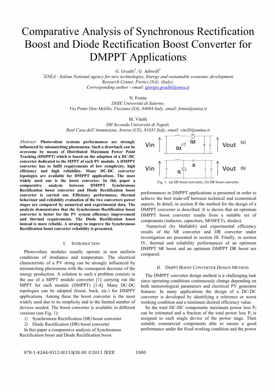
Photovoltaic modules usually operate in non uniform conditions of irradiance and temperature. The electrical characteristic of a PV string can be strongly influenced by mismatching phenomena with the consequent decrease of the energy production. A solution to such a problem consists in the use of a MPPT module converter [1] carrying out the MPPT for each module (DMPPT) [1-4]. Many DC-DC topologies can be adopted (boost, buck, etc.) for DMPPT applications. Among these the boost converter is the most widely used due to its simplicity and to the limited number of devices needed. The boost converter is available in different versions (see Fig. 1):
1) Synchronous Rectification (SR) boost converter 2) Diode Rectification (DR) boost converter In this paper a comparative analysis of Synchronous
Rectification boost and Diode Rectification boost
(b)
(a)
Vin VoutQD
Vin VoutQ1Q2
Fig. 1. (a) SR boost converter; (b) DR boost converter.
performances in DMPPT applications is presented in order to achieve the best trade-off between technical and economical aspects. In detail, in section II the method for the design of a DMPPT converter is described. It is shown that an optimum DMPPT boost converter results from a suitable set of components (inductor, capacitors, MOSFETs, diodes).
Numerical (by Matlab®) and experimental efficiency results of the SR converter and DR converter under investigation are presented in section III. Finally, in section IV, thermal and reliability performances of an optimum DMPPT SR boost and an optimum DMPPT DR boost are compared.
II. DMPPT BOOST CONVERTER DESIGN METHOD
The DMPPT converter design method is a challenging task since operating conditions continuously change depending on both meteorological parameters and electrical PV generator features. In many applications the design of a DC-DC converter is developed by identifying a reference or worst working condition and a minimum desired efficiency value.
So the total DC-DC components maximum power loss Pd can be estimated and a fraction of the total power loss Pd is assigned to each single device of the power stage. Then suitable commercial components able to ensure a good performance under the fixed working condition and the power
978-1-4244-9312-8/11/$26.00 ©2011 IEEE 1000
distribution are chosen. A crucial aspect is represented by the choice of the losses distribution among the different devices.
The designer assigns the maximum power losses to each DC-DC converter component on the strength of his/her experience and knowledge of the specific problem under investigation. There is no certainty at all that the selected distribution is the optimal choice among the possible ones.
Very often, the designer is not able to find, at the first shot, commercial devices providing the desired efficiency performances and fulfilling the assigned specifications. So the design process must be repeated again with a different distribution of losses among the various components, until a feasible solution can be identified. Unlike other applications, in a DMPPT system it is not possible to identify a worst or reference operating case and choose devices able to ensure a good performance under only that fixed working condition.
To obtain a suitable efficiency the DMPPT converter has to ensure good performances in different potential working conditions, which vary in terms of input electric parameters (power, voltage, current) with meteorological conditions changing. In this context, the losses distribution, the current and voltages ripple amplitudes and the converter components choices are crucial. Furthermore converter devices parameters are interrelated; so the selection of one of them affects the other ones choice and performances.
Our approach to develop a DMPPT converter design method [5] consists in achieving converter appropriate parameters values by means of a stochastic algorithm (Montecarlo algorithm) without any a priori designer choice of the converter variables (switching frequency, ripples, output voltage level, etc) that could badly influence the system behaviour. The proposed algorithm identifies suitable matched sets of components able to maximize the energy supplied to the converter taking into account the meteorological parameters and electrical PV generator features changing. Initial data needed for the converter design are: irradiance diagrams, PV modules characteristics and load requirements. Input voltages and currents of the boost converter can be known at any moment of the day due to the adoption of a MPPT controller able to track module maximum power point voltage and current.
Polycrystalline modules of 225Wp and the irradiance diagrams of a typical summer day of the south of Italy are considered. The DMPPT converter design used is fully described in [5]. It can be summarized as it follows:
1) switching frequency random choice in a proper range
2) converter devices random choice in commercial components databases
3) converter components constraints check: Inductor: maximum operating current Capacitors: maximum voltage ripple maximum operating voltage maximum RMS current MOSFETs: maximum drain-source voltage maximum drain current If the chosen device fulfils the constraints, it is considered suitable for the use, otherwise another
component is randomly chosen within the corresponding database and constraints are verified. When a suitable set of devices is found, it is stored in a matrix where each row contains the parameters of the different converter devices (first row-> inductor parameters, second row-> capacitor parameters, etc).
4) DMPPT losses evaluation 5) DMPPT converter efficiency performance and cost
evaluations. By repeating this process N times, N possible converter
solutions are obtained. Each of them can be characterized by two figures of merit: the first one is the converter energetic efficiency ηe, the second one is the converter cost c. The multi-objective optimization consists in the maximization of ηe and in the minimization of c. Representing the solutions in the ηe-c plane, it is possible to identify a suitable Pareto front [6]. This is the set of the best (not dominated) solutions with respect to at least one of the two objectives. This design method is applied to a DMPPT SR boost and a DMPPT DR boost converter.
III. NUMERICAL AND EXPERIMENTAL RESULTS
The DMPPT SR boost converter Pareto front generated by means of the algorithm described in Sec. II it is shown in Fig.2 and it consists of 6 different solutions, identified by an alphabetical letter, that provide different performances in terms of efficiency and cost. There are some solutions (c-f) nearly equivalent from the energetic efficiency point of view but with different costs. An optimum solution able to ensure a good efficiency and a moderate cost is the solution #d.
It represents a SR boost converter with energetic efficiency equal to 97.4% in correspondence of the irradiation profile considered and a cost of about $10. In order to verify the effectiveness of the SR boost converter design criteria a boost converter prototype has been developed in accordance with the solution #d. Many experimental tests have been carried out in order to analyze efficiency performances of the prototype. In Fig. 3a numerical and experimental data concerning the efficiency of the SR boost converter under investigation vs input power are compared. The Pareto front generated for DMPPT DR boost converter by means of the algorithm described in [5] is shown in Fig. 4. It consists of 13 different solutions, identified by a progressive number, that provide different performances in terms of efficiency and cost. Solutions 3-13 are nearly equivalent from the energetic efficiency point of view, but they have different costs. Also in this case the optimum solution is placed in the middle of the Pareto front shown.
The solution #7 concerning a converter with energetic efficiency equal to about 95.2% in correspondence of the irradiation profile considered and a cost of about $9.3, represents a good trade-off between technical and economic aspects. A DR boost converter prototype has been developed in accordance with the solution #7. Efficiency performances have been analyzed by experimental tests. In Fig. 3b numerical and experimental data concerning the efficiency of the DR boost converter under investigation vs input power are
1001

compared showing a good agreement. After the design and the performances evaluation a comparative analysis between DMPPT SR boost and DMPPT DR boost is carried out. In the power range considered DMPPT SR boost converter is characterized by higher efficiency performance than DMPPT DR converter ones as shown in Fig. 3.
cbd
a
ef
0
5
10
15
20
25
0,93 0,94 0,95 0,96 0,97 0,98
cost
[$]
energetic efficiency
cd
ef
0
5
10
15
20
25
0,973 0,974 0,975 0,976
cost
[$]
energetic efficiency (a) (b)
Fig. 2. (a) SR boost converter Pareto front; (b) Zoom of SR Pareto front.
0,90,910,920,930,940,950,960,970,980,99
120 170 220
effi
cien
cy[/
]
input power [W]
Efficiency of converter #dexperiments simulations
0,90,910,920,930,940,950,960,970,980,99
120 170 220
effi
cien
cy[/]
input power [W]
Efficiency of converter #7experiments simulations
(a) (b)
Fig. 3. Comparison of experimental and numerical results for (a) SR boost (b) DR boost.
1
2 34
5 67 89 101112
13
6
7
8
9
10
11
12
0,935 0,94 0,945 0,95 0,955
cost
[$]
energetic efficiency
345 6 7 8 9 10
11 1213
6
7
8
9
10
11
12
0,9526 0,95265 0,9527 0,95275
cost
[$]
energetic efficiency (a) (b)
Fig. 4. (a) DR boost converter Pareto front; (b) Zoom of SR Pareto front.
The efficiency performance increase of SR boost is due to lower losses than DR converter ones. As observed in Fig. 5, DR boost converter is characterized by high inductor and diode losses. In the SR boost converter (Fig. 1a) MOSFET Q2 replaces the diode D of the DR boost converter. Since Q2 on voltage is lower than the diode one, SR boost MOSFET Q2 conduction losses are lower than DR diode ones. Moreover the inductance value of the DR boost has to be high enough to avoid the DCM (Discontinuous Conduction Mode) for irradiance values higher than 100W/m2.
The SR boost converter instead works in CCM (Continuous Conduction Mode) in every operating condition. So a low inductance value can be used and then lower losses than DR ones are obtained. For a quick comparison of conversion efficiency SR boost and DR boost European efficiency are calculated:
%,972.048.01.013.006.003.0 %100%50%30%20%10%5_ =+++++= ηηηηηηη SReu
%.952.048.01.013.006.003.0 %100%50%30%20%10%5_ =+++++= ηηηηηηη DReu
where ηi% is the efficiency operating at i% of the PV module nominal power.
IV. SR BOOST AND DR BOOST RELIABILITY EVALUATION
Since in a PV system the operational life of a PV module typically exceeds twenty years, another important DMPPT converter requirements [8-10] is the reliability. Reliability R(t) is defined as the probability that an item will perform a required function without failure under stated conditions for a stated period of time. Different reliability mathematical models are available depending on the class of considered components (electronic, electric, electromechanical).
Scientific studies on the reliability of electronic devices demonstrate that a suitable model is represented by the exponential one:
,)( tetR λ−= (1) where: λ is the constant failure rate; t is the mission time.
SR boostDR boost
89
1011
1213
1415
1617
18
0
0.5
1
1.5
2
2.5
3
3.5
4
SR boodtDR boost
89
1011
1213
1415
1617
18
0
0.5
1
1.5
2
2.5
3
3.5
4
time[h]
pow
er[W
]
pow
er[W
]
pow
er[W
]
(a) (b)
(a) (b) Fig. 5. (a) SR boost and DR boost inductor losses; (b) SR boost Q2 and DR
boost D losses. A measure of a system reliability is the Mean Time
Between Failure (MTBF). High MTBF values characterize high reliability products. The converter reliability is estimated by calculating the power stage and control stage components failure rates. In this paper the reliability of the converters power stages has been evaluated by using the MIL-HDBK-217F NOTICE 2 prediction model [7]. Capacitors failure rate
Capacitors reliability depends on the device realization technology: electrolytic, tantalum, ceramic, plastic film. It is worth noting that electrolytic capacitors have the worst reliability performance, while plastic film components are the most reliable ones. DMPPT applications are characterized by high power high voltages rates, so large capacitance values are needed. In these cases electrolytic capacitors are frequently used. The capacitors failure rate is given by (2): (2) where: λb_Cap is the input capacitor base failure rate; πT is the temperature factor; πCap is the capacitance factor; πV is the capacitor voltage stress factor; πSR is the series resistance factor;
,_ EQSRVCapTCapbCap ππππππλλ =
1002

πQ is the quality factor; πE is the environment factor.
Capacitors π factors are indicated in Section 10.1 of the MIL-HDBK-217F. The SR boost capacitors failure rates are:
,10/0043.0 6_ hoursfailuresSRCin =λ (3)
,10/0052.0 6_ hoursfailuresSRCout =λ (4)
while the DR boost capacitors failure rates are: ,10/0036.0 6
_ hoursfailuresDRCin =λ (5)
.10/0052.0 6_ hoursfailuresDRCout =λ (6)
Inductor failure rate
Magnetic devices are more reliable than other components, their main failure mode depends on the copper winding insulation fail that causes a short between adjacent turns resulting in hot spots. The formula for the calculation of inductor failure rate is:
,_ EQTInductorbInductor πππλλ = (7) where: λb_Inductor is the inductor base failure rate; πT is the temperature factor; πQ is the quality factor; πE is the environment factor.
Inductors factors values are indicated in Section 11.2 of the MIL-HDBK-217F. The SR and DR boost inductor failure rates are shown in (8) and (9):
,10/10*5.1 64_ hoursfailuresSRInductor
−=λ (8)
.10/10*9.1 64_ hoursfailuresDRInductor
−=λ (9) Semiconductor devices failure rate
Semiconductor components suffer electrical stresses, intrinsic and extrinsic failures. Overstressing and electrostatic discharge may cause devices failure . Also extrinsic failures, as wrong interconnection and packaging of chips, or intrinsic failure as defects or metallization may damage MOSFETs and diodes. MOSFETs failure rates can be estimated by (10):
,_ EQATMOSbMOS ππππλλ = (10) where: λb_MOS is the MOSFET base failure rate; πQ is the quality factor; πE is the environment factor; πT is the temperature factor; πA is the application factor.
Equation (11) is used to calculate the temperature factor:
,))2981
2731(*1925(e TjT
−+
−=π (11) where Tj is the MOSFET junction case temperature.
Other MOSFET factors values are indicated in Section 6.4 of the MIL-HDBK-217F NOTICE 2. Diodes failure rate formula is:
,_ EQCSTDIODEbDIODE πππππλλ = (12)
where: λb_DIODE is the diode base failure rate; πT is the temperature factor; πS is the voltage stress factor; πC is the contact construction factor; πQ is the quality factor; πE is the environment factor.
The MIL-HDBK-217F[7] indicates diode π factors in section 6.1. Equation (13) is used to evaluate the diode πT factor.
.))2981
2731(*3091(e TjT
−+
−=π (13)
The diode temperature factor is computed with the same method seen for the MOSFET one, the only difference is represented by the MOSFET coefficient 1925 substituted by the value 3091 in the diode expression due to the more reliable diode behavior. Equations (11) and (13) show that the device junction temperature strongly influences the component reliability. A necessary requirement for the safety and then the reliability of a semiconductor device is that its junction temperature is lower than the specified maximum value provided by components suppliers on datasheets. This is a crucial issue in DMPPT applications since the operating conditions change continuously and they can expose the DC-DC converter to thermal stresses. The operating junction temperature of a semiconductor device is given by (14).
,* _ jathdaj RPTT += (14) where: Tj is the semiconductor device junction case temperature Ta is the ambient temperature; Pd is the semiconductor device dissipated power; Rth_ja is the semiconductor device junction-to-ambient thermal resistance indicated by device manufacturer.
Under the considered irradiance distribution the worst case, from the thermal point of view, is at mid-day when an irradiance level of about 1000W/m2 is achieved. In this operating condition, the semiconductor devices junction temperatures for the SR and DR boost considered are:
;50_1_ CT SRQj °= ;37_2_ CT SRQj °=
;188__ CT DRMOSj °= .187__ CT DRDiodej °=
The SR MOSFETs junction temperatures are lower than the maximum values provided on datasheets, while the DR semiconductor devices junction temperatures are higher than those indicated by suppliers. So the DR boost converter needs suitable heat-sinks. Their thermal resistance can be calculated by means of (15):
,___
___ cdthjcth
MAXd
MAXaMAXjdath RR
PTT
R −−−
= (15)
where: Rth_da is the heat-sink to ambient thermal resistance; Rth_jc is the switching device junction to case thermal
1003

resistance; Rth_cd is the case to heat-sink thermal resistance; Ta_MAX is the maximum ambient temperature; Tj_MAX is the maximum junction temperature; Pd_MAX is the total power loss of the semiconductor device.
For the DR boost the MOSFET heat-sink thermal resistance must be lower than 54°C/W, while the diode one must be lower than 43°C/W. As shown in Fig. 6 the converter MTBF is influenced by heat-sinks thermal resistance. It is clear that choosing a low Rth_da it is possible to obtain a more reliable converter. For the DR boost considered two heat-sinks characterized by a thermal resistance of 13°C/W are used. In that condition DR boost semiconductor components failure rates are:
,10/6775.1 6_ hoursfailuresDRMOS =λ (16)
.10/0096.0 6_ hoursfailuresDRDiode =λ (17)
The MTBF of the DR boost power stage is evaluated by means of the following expressions:
(18) As shown previously, for the junction temperatures
reached, the SR boost converter does not need heat-sinks. MOSFETs failure rates are:
,10/2595.1 6_1 hoursfailuresSRQ =λ (19)
.10/3083.1 6_2 hoursfailuresSRQ =λ (20)
The MTBF of the SR boost power stage can be calculated
by the next formula. (21)
It is evident that the power stage of the SR converter is less reliable than the DMPPT DR one. The reliability decrease of the SR boost is due to the presence of two MOSFETs. In fact MOSFETs are the less reliable power stage devices. In spite of this, it is possible to improve the SR boost reliability using a suitable heat-sink for each switching devices also if the junction temperature is not higher than the maximum junction temperature specified by manufacturers. The converter MTBF vs heat-sink thermal resistance is shown in Fig. 7. For the SR boost considered two heat-sinks characterized by a thermal resistance of 13°C/W are used. In this condition MOSFETs failure rates are:
,10/8645.0 6__1 hoursfailureshsSRQ =λ (22)
.10/0238.1 6__2 hoursfailureshsSRQ =λ (23)
In this case the MTBF of the SR boost power stage is:
(24)
Equation (24) demonstrates that SR boost reliability performances comparable with the DR ones can be obtained choosing suitably semiconductor devices heat-sinks.
0
0,1
0,2
0,3
0,4
0,5
0,6
0,7
0 10 20 30 40 50
MTB
F [1
06ho
urs
]
Rth_da[°C/W]
DR boost
0
0,1
0,2
0,3
0,4
0,5
0,6
0,7
0 10 20 30 40 50
MTB
F [1
06h
ou
rs]
Rth_da[°C/W]
SR boost
Fig. 6. DR boost MTBF vs Rth_da. Fig. 7. SR boost MTBF vs Rth_da
I. CONCLUSION
In this paper a comparative analysis between a DMPPT SR boost and a DMPPT DR boost converter is presented. The design guidelines for the optimization of DMPPT boost converter are described. Good performances of the DMPPT converter can be obtained by choosing a suitable set of devices. This optimum set can be identified by means of a stochastic algorithm that generates the Pareto front of not dominated solutions with respect to energetic efficiency and cost. In order to verify the effectiveness of the proposed design criteria, two prototypes have been developed in accordance with the solution #d of the SR boost Pareto Front and in accordance with the solution #7 of the DR boost Pareto front. Many experimental tests have been carried out in order to analyze and compare the efficiency and thermal behaviour of the two solutions. Reliability evaluations have been calculated for both converters power stages. These analyses and tests demonstrate that the Synchronous Rectification boost has better efficiency and thermal performance than the Diode Rectification one. On the other hand the DR boost assures a higher reliability. A SR boost MTBF performance comparable with the DR boost one can be obtained using suitable MOSFETs heat-sinks. So the DMPPT DC-DC converter choice is a trade-off between efficiency, thermal and reliability requirements.
VI. REFERENCES
[1] N. Femia, G. Lisi, G. Petrone, G. Spagnuolo, M.Vitelli, ”Distributed Maximum Power Point Tracking of Photovoltaic Arrays: novel approach and system analysis,” IEEE Transactions on Industrial Electronics, vol. 55, p. 2610-2621, June 2008.
[2] G.R. Walker, P.C. Sernia, “Cascaded dc-dc Converter Connection
of Photovoltaic Modules,’’ IEEE Transactions on Power Electronics, vol. 19, p. 1130-1139, July 2004.
[3] E. Roman, R. Alonso, P. Ibanez, D. Goitia, D., S. Elorduizapatarietxe,
S.,’’ Intelligent PV Module for Grid-Connected PV Systems,’’ IEEE Transactions on Industrial Electronics, vol. 53, p. 1066-1073, June 2006.
[4] W. Xiao, N. Ozog, W.G. Dunford,’’ Topology Study of Photovoltaic
Interface for Maximum Power Point Tracking,’’ IEEE Transactions on Industrial Electronics, vol. 54, p. 1696-1704, June 2007.
[5] N. Femia, G. Petrone, G. Spagnuolo, G. Adinolfi, M. Vitelli, ”Design of dc/dc Converters for DMPPT PV Applications Based on the Concept of Energetic Efficiency,” Journal of Solar Energy Engineering, vol.132, May 2010.
[6] K. Deb, “Multi-Objective Optimization using Evolutionary Algorithms”, John Wiley & Sons, 2002.
.10*58.01 6
___ hoursMTBF
OutCapInCapIndcctorDRDiodeDRMOSboostDR =
++++=
λλλλλ
.10*38.01 6_
_2_1
hoursMTBFOutCapInCapInductorQQ
boostSRSRSR
=++++
=λλλλλ
.10*52.01 6
__
_2__1
hoursMTBFOutCapInCapInductorhsQQ
boostSRSRhsSR
=++++
=λλλλλ
1004

[7] MIL-HDBK -217F. [8] H. Calleja, F. Chan, I. Uribe, “Reliability-Oriented Assessment of a
DC-DC Converter for Photovoltaic Applications,” IEEE Power Electronics Specialist Conference 2007, p.1522-1527, June 2007
[9] X. Tian, “ Design for Reliability and Implementation on Power Converters”, Reliability and Maintainability Symposium Proceedings, p.89-95, January 2005.
[10] G. Graditi, D. Colonnese, N. Femia, “ Efficiency and Reliability Comparison of DC-DC Converters for Single Phase Grid Connected Photovoltaic Inverters”, Symposium on Power Electronics, Electrical Drives, Automation an Motion Proceedings, p.140-147, June 2010.
1005


