Embed Size (px)
Citation preview

Coulomb drag in graphene – boron nitride heterostructures: the effect of virtualphonon exchange
Bruno Amorim,1 Jurgen Schiefele,2 Fernando Sols,2 and Francisco Guinea1
1Instituto de Ciencia de Materiales de Madrid, CSIC, Cantoblanco, E-28 049, Madrid, Spain2Departamento de Fısica de Materiales, Universidad Complutense de Madrid, E-28 040, Madrid, Spain
(Dated: September 28, 2012)
For a system of two spatially separated monoatomic graphene layers encapsulated in hexagonalboron nitride, we consider the drag effect between charge carriers in the Fermi liquid regime. Com-monly, the phenomenon is described in terms of an interlayer Coulomb interaction. We show thatif an additional electron – electron interaction via exchange of virtual substrate phonons is includedin the model, the predicted drag resistivity is modified considerably at temperatures above 150 K.The anisotropic crystal structure of boron nitride, with strong intralayer and comparatively weakinterlayer bonds, is found to play an important role in this effect.
I. INTRODUCTION
If two systems containing mobile charge carriers arespatially separated such that direct charge transfer isnot possible, but close enough to allow interaction be-tween the carriers in different layers, the resulting mo-mentum transfer will equalize the drift velocities in bothsystems. This frictional effect was experimentally ob-served between (quasi) two-dimensional electron gases indouble quantum well structures1,2. In most of the theo-retical work the interlayer interaction was attributed toCoulomb scattering, hence the effect now bears the name‘Coulomb drag’ (see Refs. 3–5).
Interest in the subject has been revived recently bythe experimental progress which made it possible to pre-pare two-dimensional electron systems based on mono-layer graphene. A considerable number of theoreticalworks6–16 studied Coulomb drag between massless Diracfermions, which effectively describe the charge carriers ingraphene17. However, a quantitatively correct explana-tion of the experimental data is still lacking6,18–20.
In the typical experiment, Coulomb drag is studied bydriving a constant current I2 through one of the layers(the active one, labeled by the index λ = 2 in Fig. 1).If no current is allowed to flow in the other (passive, in-dex 1) layer, a potential difference V1 builds up there.In terms of these two quantities, the drag resistivityρD ≡ (W/L)V1/I2 serves as a measure of the momen-tum transfer between the two layers, where W and Lare, respectively, the width and the length of the layer. Atheoretical expression for ρD in second order in the inter-layer interaction can be derived either using Boltzmann’skinetic equation4,10,11,21 or the Kubo formula5,9,11.
In the present work, we focus on the interlayer interac-tion responsible for the drag effect in heterostructurescomposed of two graphene monolayers and hexagonalboron nitride (hBN), see Fig. 1. The large bandgap in-sulator hBN has a layered structure composed of stackedhexagonal crystal planes. Recently the material receivedmuch attention as it allows the construction of graphene– hBN devices with, in comparison to the much usedSiO2 substrates, favorable high carrier mobilities22–25. In
I
II
IIIΛ = 1
Λ = 2
z = 0
z = d
FIG. 1. A sketch of the double layer system under consid-eration. The two monoatomic graphene layers (yellow) withcharge carrier concentration n1, n2 are placed at z = 0 andz = d and labelled by the layer index λ = 1, 2, respectively.The surrounding space (regions I, II, and III) is filled withthe insulating material boron nitride with hexagonal struc-ture (hBN).
particular, the Manchester group reported the fabrica-tion of devices where a few layer thin hBN crystal, ob-tained by exfoliation, is sandwiched between two mono-layers of graphene26–28. If such a structure is used for aCoulomb drag experiment, the Dirac fermions in the ac-tive and passive layer can exchange momentum not onlyvia Coulomb interaction but also by phonon exchangethrough the spacer medium. The effect of a combinedCoulomb-phonon coupling on the drag resistivity has pre-viously only been studied for quasi two dimensional elec-tron gases in semiconductor systems29–34.
In the following, we first investigate the effects of theanisotropy of hBN, where the bonds in between thegraphene-like planes are much weaker than the in-planebonds, on the electron – electron interaction via phononexchange. We then show that the inclusion of phononexchange into the description of Coulomb drag can sig-nificantly alter the temperature, density and distance de-pendence of the predicted value for ρD at temperaturesabove 150 K.
arX
iv:1
206.
0308
v2 [
cond
-mat
.mes
-hal
l] 2
8 Se
p 20
12

2
II. INTERLAYER INTERACTION
A. Combined Coulomb – phonon mediatedinteraction
In a two-layer system as shown in Fig. 1, where the re-gions I, II and III are filled with a homogeneous isotropicdielectric medium, the Fourier transform of the bare (un-screened) Coulomb potential between electrons in layersλ and λ′ has the form
V(0)λλ′ (q) =
1
ε∞
e2
2εvacqe−qd(1−δλλ′ ) , (1)
where q = (qx, qy), εvac denotes the dielectric constant ofvacuum and ε∞ accounts for the high frequency screen-ing properties of the medium. Apart from this Coulombinteraction, the charge carriers in each graphene layer in-teract via a substrate phonon mediated interaction. Thecharge carriers from each layer couple to the long rangeelectric fields generated by optically active phonon modesin the surrounding material via Frohlich coupling35–37.This remote interaction between carriers in graphene andoptical phonon modes in a substrate medium was foundto influence the electrical conductivity of graphene on adielectric substrate24,38,39.
In Appendix A, we show that in an isotropic medium,the combined interaction between electrons in layers λand λ′ via the effects of a static Coulomb potentialand virtual substrate phonon exchange is of the formof Eqn. (1), with ε∞ replaced by the frequency depen-dent dielectric function ε(ω) of the substrate material(see Eqn. (A7)).
In the following, we specialize to the anisotropic spacermaterial hBN. From its three acoustic and nine opticalphonon bands, only those that (via dipole oscillations)create long range electric fields couple to the grapheneelectrons40. Given the layered uniaxial crystal struc-ture of hBN, these (infrared active) optical modes aredescribed by a dielectric tensor of the form41
ε(ω) = diag[ε⊥(ω), ε⊥(ω), ε‖(ω)
]. (2)
The resonance frequencies ω‖TO and ω⊥TO of the two
retarded42 dielectric functions
ε⊥,‖(ω) = ε⊥,‖∞ + f⊥,‖
(ω⊥,‖TO
)2(ω⊥,‖TO
)2 − ω2 − iωγ⊥,‖, (3)
are the phonon frequencies at the Γ point for trans-verse intraplane shear modes with displacements paralleland perpendicular to the c-axis of the crystal (alignedwith the z direction in Fig. 1), respectively. We makethe usual approximation of dispersionless optical phononbands.29,35,43 The values for the high frequency dielec-tric constants ε∞, the oscillator strengths f (related tothe static, ε0, and high frequency dielectric constants,f = ε0− ε∞), ωTO and the damping factors γ taken fromRef. 44 are listed in Table I.
To obtain the combined Coulomb-phonon interaction
U(0)λλ′ in the anisotropic medium, we solve Poisson’s equa-
tion
−∇ · (ε · ∇φ) = ρfree/εvac
with ρfree being the free charge density of a point charge−e at the origin. With Eqn. (2), Poisson’s equation be-comes
− ∂
∂z
(ε‖∂
∂zφ(q, z)
)+ q2ε⊥φ(q, z) = − e
εvacδ(z) ,
and as U(0)12 = −eφ(q, d) and U
(0)11 = U
(0)22 = −eφ(q, 0) we
get
U(0)λλ′(q, ω) =
e2
2εvacε‖(ω)q
√ε‖(ω)
ε⊥(ω)(4)
× exp
[−qd(1− δλλ′)
√ε⊥(ω)
ε‖(ω)
].
A generalization of this result to structures where theregions I,II, and III (see Fig. 1) are filled with different
insulating materials (or air) is straightforward; U(0)11 then
involves different dielectric functions than U(0)22 .
B. RPA screened interlayer interaction
To take into account the screening properties of theconduction electrons in the graphene layers themselves,we employ the standard procedure of solving the Dysonequation for the two-layer system within the randomphase approximation (RPA) (see Ref. 5). This finallyyields the dressed interlayer interaction
U12(q, ω) =U
(0)12 (q, ω)
εRPA(q, ω). (5)
The total screening function for the coupled electron-phonon system given by (see Ref. 31 and Appendix B)
εRPA = (1− U (0)11 χ1)(1− U (0)
22 χ2)− U (0)12 U
(0)21 χ1χ2 , (6)
where χ1,2 denotes the (frequency and momentum de-pendent) polarizability of the graphene layers45.
Fig. 2 shows a density plot of |εRPA(q, ω)|, using dimen-sionless units x = q/kF and y = ω/(vF kF ), where kFis the Fermi momentum. The horizontal dashed greenlines mark the transverse and longitudinal frequenciesof the infrared active modes in hBN, connected by theLyddane-Sachs-Teller relation46 ω2
LO/ω2TO = ε0/ε∞. For
small damping γ ωTO, the real parts of ε⊥,‖(ω) are
close to a pole at ω⊥,‖TO and close to zero at ω
⊥,‖LO , re-
spectively. Near these frequencies, the absolute valueof the total screening function εRPA likewise shows anabrupt change from high values (light colors) to almostzero (dark colors). In regions where |εRPA| is small, thered lines Re εRPA = 0 show the coupled plasmon-phonondispersion relation of the two-layer system.

3
FIG. 2. Absolute value of the total screening function εRPA
Eqn. (6), with n1 = n2 = 0.02 nm−2 and d = 8 nm. Vertical
green lines show the optical resonance frequencies ω‖TO, ω
‖LO,
ω⊥TO, and ω⊥LO of hBN (bottom to top). Red curves markthe zeros of Re εRPA. The dashed black lines show the liney = x and mark the region where Imχ = 0. The hybridizationbetween phonon and plasmon modes is clear.
20 50 100 200 300
0.001
0.01
0.1
1
T @KD
ÈΡ DÈ@
WD
d = 8 nmd = 6 nmd = 4 nmd = 2 nm
FIG. 3. Drag resistivity versus temperature for various in-terlayer distances, n = 0.02 nm−2. The blue curves show|ρD| (Eqn. (7)) including interaction via phonon exchangeand Coulomb interaction, the dashed red curves show |ρCD|(Eqn. (9)) with Coulomb interaction only, and dashed blacklines the low-temperature asymptote ρlowT
CD (Eqn. (B2)). Thelowest pair of curves (d = 8 nm) is also plotted on a linearscale in Fig. 7.
III. RESULTS FOR THE DRAG RESISTIVITY
In the following, we assume for the sake of simplic-ity the same positive carrier density n (corresponding toelectron doping) in both layers, such that EF kBT . Inparticular, we do not address the recently reported dragat charge neutrality point20, which was attributed eitherto contributions from higher order perturbation theory15
or to correlated density inhomogenities in the graphenelayers16,20.
0.010 0.015 0.020 0.025 0.030-0.7
-0.6
-0.5
-0.4
-0.3
-0.2
-0.1
0.0
n @nm-2D
ΡD
@WD
T=
300
K
T = 200 K
T = 100 K
FIG. 4. Drag resistivity versus carrier density for varioustemperatures, d = 8 nm. Colors as in Fig. 3.
0.1 0.5 1.0 5.0 10.0 50.0
0.001
0.01
0.1
1
10
d @nmDÈΡ D
È@W
D
FIG. 5. Drag resistivity versus layer separation for T = 300 K,n = 0.02 nm−2. Colors as in Fig. 3. The low-temperatureasymptote ρlowT
CD (dashed black curve, Eqn. (B2)), con-
verges for large layer separation to ρlarge dCD (dotted green line,
Eqn. (10)). Note that at this temperature and density ρlowTCD
already differs from the full static calculation, ρCD.
0.0 0.2 0.4 0.6 0.8 1.00
1
2
3
4
y = ΩHvF kF L
KHT
TF
L-2
10
4
T=
200K
T=
100K
T=
70K
FIG. 6. The integral kernel K of Eqn. (8) with x = q/kF = 1,d = 8 nm, n = 0.02 nm−2 as a function of y = ω/vF kF for thetemperatures 200, 100, 70 K (full curves, from top to bottom).The curves have been aligned on the left side by dividingwith the y → 0 temperature dependence (T/TF)2. At T =
100 K (green curve) a peak near the resonance frequency ω‖TO
appears, at T = 200 K (blue curve) there is and additionalsecond peak near ω⊥TO (see the vertical green lines in Fig. 2).Dashed curves show the integral kernel for ρCD, where thesepeaks are absent.
4
The drag resistivity then assumes a negative value18,and the first non-vanishing contribution to ρD obtainedin perturbation theory is of second order in the dressedinterlayer interaction4,5. In terms of the variables carrierdensity, layer separation, and temperature, and underthe assumptions that both layers are with high electrondoping and T TF
47, it reads (refer to Refs. 6 and 10for details)
ρD = − ~e2
α2g
8
~vF√πn
kBT
∫ ∞0
dx
∫ ∞0
dy K(T, d, n) , (7)
where αg = e2/(4πεvacvF~) denotes the effective finestructure constant in graphene and the integral kernel
K =k2F ε
2vac
e4
|U12(x, y)|2
sinh2(y TF2T
) x7 Φ2(x, y)
x2 − y2. (8)
The function Φ, defined in Eqn. (B1), is related to thenonlinear susceptibility of graphene, and restricts the in-tegration range in the x, y-plane to the region ω < vF q.
In order to estimate the contribution of phonon ex-change to the drag effect, we note that the drag resistiv-ity ρCD resulting from Coulomb interaction only (which isusually taken as a measure for Coulomb drag) is obtainedby substituting the static value of the electron-electroninteraction into the integral kernel Eqn. (8):
ρCD = ρD∣∣U
(0)
λλ′ (q,ω=0). (9)
For low temperatures EF kBT , the resistivity ρCD canbe approximated by ρlow T
CD ∝ T 2 of Eqn. (B2) (see Ref. 6for a detailed derivation), under the additional conditionkF d, kF d/ε‖ 1 (large layer spacing), this can be further
approximated to yield6
ρlarge dCD = − ~
e2
(ε‖0
)3ε⊥0
ζ(3)
π28α2g
(kBT )2
(~vF )2n3d4. (10)
(Note that in the static limit, one only needs to rescaled→ d
√ε⊥/ε‖ and αg → αg/
√ε⊥ε‖ to take into account
the anisotropy of hBN.) The full blue curves in Figures3-5 show the absolute value of ρD Eqn. (7) for differentparameters T , n, and d, while |ρCD| is shown by dashedred curves, ρlow T
CD by the dashed black lines in Figures 3
and 5, and the dotted green line in Fig. 5 shows ρlarge dCD .
As Figures 3 and 4 show, the contribution of phononmediated interaction to the drag resistivity is vanish-ingly small at low temperatures, but becomes notice-able for T > 150 K, the effect being more pronouncedthe larger the layer separation. This temperature de-pendence is due the factor sinh−2[yTF /(2T )] in the inte-gration kernel Eqn. (8), which suppresses the integrandfor values of y > T/TF . Thus at low temperatures,the main contribution to the y-integration in Eqn. (7)comes from a frequency range where the dielectric func-tions in the integrand are still close to their static val-ues. However, the phonon contribution becomes notice-able at lower temperatures than one would expect, tak-ing into account that the energy of the lowest phonon
50 100 150 200 250 3000.00
0.05
0.10
0.15
0.20
T @KD
ÈΡ DÈ@
WD
isotropy, Ε¦
isotropy, Εþanisotropy
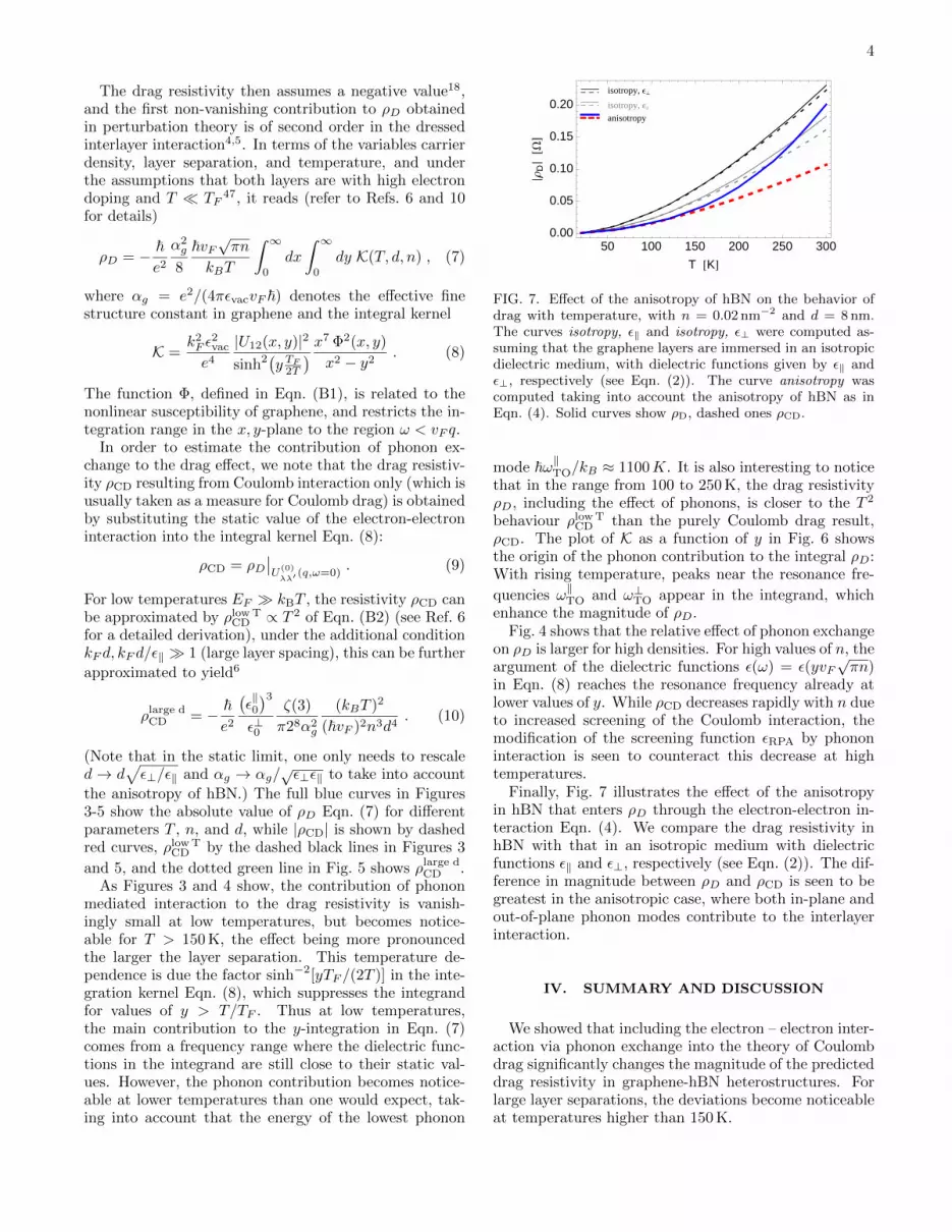
FIG. 7. Effect of the anisotropy of hBN on the behavior ofdrag with temperature, with n = 0.02 nm−2 and d = 8 nm.The curves isotropy, ε‖ and isotropy, ε⊥ were computed as-suming that the graphene layers are immersed in an isotropicdielectric medium, with dielectric functions given by ε‖ andε⊥, respectively (see Eqn. (2)). The curve anisotropy wascomputed taking into account the anisotropy of hBN as inEqn. (4). Solid curves show ρD, dashed ones ρCD.
mode ~ω‖TO/kB ≈ 1100K. It is also interesting to noticethat in the range from 100 to 250 K, the drag resistivityρD, including the effect of phonons, is closer to the T 2
behaviour ρlow TCD than the purely Coulomb drag result,
ρCD. The plot of K as a function of y in Fig. 6 showsthe origin of the phonon contribution to the integral ρD:With rising temperature, peaks near the resonance fre-
quencies ω‖TO and ω⊥TO appear in the integrand, which
enhance the magnitude of ρD.Fig. 4 shows that the relative effect of phonon exchange
on ρD is larger for high densities. For high values of n, theargument of the dielectric functions ε(ω) = ε(yvF
√πn)
in Eqn. (8) reaches the resonance frequency already atlower values of y. While ρCD decreases rapidly with n dueto increased screening of the Coulomb interaction, themodification of the screening function εRPA by phononinteraction is seen to counteract this decrease at hightemperatures.
Finally, Fig. 7 illustrates the effect of the anisotropyin hBN that enters ρD through the electron-electron in-teraction Eqn. (4). We compare the drag resistivity inhBN with that in an isotropic medium with dielectricfunctions ε‖ and ε⊥, respectively (see Eqn. (2)). The dif-ference in magnitude between ρD and ρCD is seen to begreatest in the anisotropic case, where both in-plane andout-of-plane phonon modes contribute to the interlayerinteraction.
IV. SUMMARY AND DISCUSSION
We showed that including the electron – electron inter-action via phonon exchange into the theory of Coulombdrag significantly changes the magnitude of the predicteddrag resistivity in graphene-hBN heterostructures. Forlarge layer separations, the deviations become noticeableat temperatures higher than 150 K.

5
TABLE I. Parameters for the dielectric function of hBN (seeEqn. (3)) taken from Ref. 44a.
ε⊥ ε‖
ε∞ 4.95 4.10
f 1.868 0.532
γ 3.61 meV 0.995 meV
ωTO 170 meV 97.4 meV
a The experimental data in Ref. 44 exhibits two resonances, astrong and a weaker one, for each direction of the polarizationof incident light. The weaker ones are attributed tomissorientation of the polycrystalline samples.
As the lowest phonon resonance frequency in the spacermaterial hBN corresponds to a temperature of approxi-mately 1100 K, our result at first sight seems to be atodds with the notion that phonon effects should be pro-portional to the thermal population factor of the relevantmodes. This is indeed the case for other transport phe-nomena, like the substrate limited electron mobility ingraphene, where real momentum transfer from an elec-tronic state (in graphene) to a phonon mode (in a di-electric substrate material) plays a role24,38. The decayrate of the electronic state is then overall proportional tothe thermal population of the phonon mode. Our sce-nario however involves the exchange of virtual phononsin a process that is of second order in the interlayerinteraction5, and no decay processes into real phononstates are relevant for ρD. We note that in Ref. 7, theeffect of substrate phonons on Coulomb drag was consid-ered for the case where a material described by a uniformdielectric function fills what is our region III of Fig. 1, anda deviation from the low-temperature T 2 behavior of ρDwas predicted for temperatures roughly an order of mag-nitude lower than the phononic resonance frequency ofthe substrate material.
Up to date, there remains considerable discrepancybetween experimental data on Coulomb drag betweengraphene layers embedded in SiO2/Al2O3
18,19 and hBN20
and the existing theoretical work. For hBN, the reporteddrag resistivities in the Fermi liquid regime are roughlya factor of three larger than predicted, and the results ofthe present paper do not change this situation. The ex-perimentally reported T 2 dependence of ρD for d = 6 nmand n = 0.018 nm−2 up to temperatures of 240 K48 doesnot disagree with our results presented in Fig. 3. Ac-tually, it appears that in the temperature range of 100to 250 K the inclusion of phonon mediated interactionbrings the behaviour of drag closer to the low temper-ature T 2 behaviour than with static Coulomb interac-tion only. Nevertheless, an extension of the experimentaldata shown in Ref. 20 up to room temperature would beneeded to distinguish clearly between ρD and ρCD. Theuse of other substrate materials, such as SiO2, shouldnot qualitatively alter the results of this paper. We thinkthat future experiments with devices as considered in the
present work will be able to check our predictions.
ACKNOWLEDGMENTS
The authors would like to thank N.M.R. Peres foruseful discussions. Financial support from Fundacaopara a Ciencia e a Tecnologia (Portugal) through GrantNo. SFRH/BD/78987/2011 (B.A.), the Marie Curie ITNNanoCTM (J.S.) and from MICINN (Spain) throughGrant No. FIS2010-21372 (F.S.) and FIS2008-00124(F.G.) is acknowleged.
Appendix A: Frohlich electron–phonon coupling andphonon mediated electron–electron interaction
Throughout the present work, we assume the dielec-tric properties of hBN layers forming heterostructures asshown in Fig. 1 to be the same as for bulk hBN.
The Frohlich Hamiltonian describing the coupling ofelectrons to a bulk polar longitudinal phonon mode (inan isotropic homogeneous dielectric material) is givenby35–37
He−ph =
∫d3rρ(r)
1√V
∑Q
M(Q)eiQ·r(aQ − a†−Q
),
where ρ(r) denotes the electron density operator, a†Q(aQ) the creation (annihilation) phonon operator withmomentum Q = (qx, qy, qz) and the matrix element reads
M(Q) = i
√e2ωLO
2εvacQ2
(1
ε∞− 1
ε0
), (A1)
with the longitudinal optical phonon frequency ωLO. Thephonon mediated interaction between electrons is givenby
ψ(Q,ω) = M(Q)M(Q)∗DLO(Q,ω), (A2)
with the bare phonon propagator
DLO(Q,ω) = 2ωLO/(ω2 − ω2
LO
). (A3)
We employ the usual approximation of dispersionless op-tical phonons29,33,35,43.
The bare Coulomb interaction is given by
VC = e2/(εvacε∞Q
2), (A4)
where ε∞ takes into account the high frequency screeningproperties of the medium.
With Eqns. (A2)-(A4) and the Lyddane-Sachs-Tellerrelation46 ω2
LO/ω2TO = ε0/ε∞, we arrive at the combined
Coulomb and phonon mediated interaction
U(Q,ω) = VC(Q) + ψ(Q,ω) =e2
εvacε(ω)Q2, (A5)

6
with ε(ω) the dielectric function of the medium, seeEqn. 3. Since the Frohlich coupling is derived in a phe-nomenological approach based on the dielectric proper-ties of the material, the combined Coulomb and phononmediated interaction simply reduces to the Coulomb in-teraction screened by ε(ω), as it should.
In a two-layer system as shown in Fig. 1, the Frohlichcoupling coupling between bulk phonons and 2D elec-trons of layer λ is given by43
Mλ(q, qz) = i
√e2ωLO
2εvac(q2 + q2z)
(1
ε∞− 1
ε0
)eiqzd(1−δλ1) ,
(A6)
where q = (qx, qy) is a two-dimensional momentum vec-tor. In analogy to the above, we now get for the combinedCoulomb–phonon interaction in a homogeneous isotropicmedium
U isoλλ′(q, ω) ≡ Vλλ′(q) + ψλλ′(q, ω)
=1
ε(ω)
e2
2εvacqe−qd(1−δλλ′ ) . (A7)
Although it is possible to generalize the Frohlichelectron–phonon coupling for the case of anisotropicmaterials41,49 and inhomogeneous layered materials50,the easiest way to obtain the effective electron–electroninteraction, taking into account the phonon mediated in-teraction, is by solving Poisson’s equation for the elec-tric potential created by a point charge in the dielectricmedium taking into account the frequency dependence ofits dielectric tensor.
Appendix B: Mathematical details
The dressed interlayer interaction Eqn. (5) is the solu-tion of the coupled set of Dyson equations
U12(q, ω) =1 2
q, ω
=1 2
q+
2∑λ=1
1 2λ λ
+1 2
q, ω+
2∑λ=1
1 2λ λ ,
where the dashed and wiggled lines denote the bareCoulomb and phonon interaction, respectively, and thefull curves electron propagators (see Refs. 5 and 31).
The function Φ(x, y) appearing in Eqn. (8) reads6,10
Φ(x, y) = Φ+(x, y) Θ(y − x+ 2)Θ(x− y)
+ Φ−(x, y) Θ(1− y − |1− x|) , (B1)
where
Φ± = ± cosh−1
(2± xy
)∓ 2± x
y
√(2± xy
)2
− 1 .
For the low-temperature approximation of ρD, the fac-tor sinh−2[yTF /(2T )] in the integration kernel Eqn. (8),which suppresses the integrand for values of y > T/TF ,allows one to expand the remaining integrand to the low-est order of y. The y integration can then be performed,yielding
ρlow TCD = − ~
e2
2πα2eff(kBT )2
3n(~vF )2
∫ 2
0
dx
e−2dx
√πnε⊥0 /ε
‖0
x3(4− x2)[(x+ 4αeff)2 − 16α2
eff exp(−2dx
√πnε⊥0 /ε
‖0
)]2
(B2)
where αeff ≡ αg/√ε⊥0 ε‖0 (see Ref. 6 for details).
1 T. J. Gramila, J. P. Eisenstein, A. H. MacDonald, L. N.Pfeiffer, and K. W. West, Phys. Rev. Lett. 66, 1216 (1991).
2 U. Sivan, P. M. Solomon, and H. Shtrikman, Phys. Rev.Lett. 68, 1196 (1992).
3 L. Zheng and A. H. MacDonald, Phys. Rev. B 48, 8203(1993).
4 K. Flensberg, B. Y.-K. Hu, A.-P. Jauho, and J. M. Kinaret,
Phys. Rev. B 52, 14761 (1995).5 A. Kamenev and Y. Oreg, Phys. Rev. B 52, 7516 (1995).6 B. Amorim and N. M. R. Peres, Journal of Physics: Con-
densed Matter 24, 335602 (2012).7 M. Carrega, T. Tudorovskiy, A. Principi, M. I. Katsnelson,
and M. Polini, New Journal of Physics 14, 063033 (2012).8 M. I. Katsnelson, Phys. Rev. B 84, 041407 (2011).

7
9 B. N. Narozhny, M. Titov, I. V. Gornyi, and P. M. Ostro-vsky, Phys. Rev. B 85, 195421 (2012).
10 N. M. R. Peres, J. M. B. L. dos Santos, and A. H. C. Neto,EPL (Europhysics Letters) 95, 18001 (2011).
11 E. H. Hwang, R. Sensarma, and S. Das Sarma, Phys. Rev.B 84, 245441 (2011).
12 W.-K. Tse, B. Y.-K. Hu, and S. Das Sarma, Phys. Rev. B76, 081401 (2007).
13 S. M. Badalyan and F. M. Peeters, ArXiv e-prints (2012),1204.4598.
14 B. Scharf and A. Matos-Abiague, Phys. Rev. B 86, 115425(2012).
15 M. Schutt, P. M. Ostrovsky, M. Titov, I. V. Gornyi,B. N. Narozhny, and A. D. Mirlin, ArXiv e-prints (2012),1205.5018.
16 J. C. W. Song and L. S. Levitov, ArXiv e-prints (2012),1205.5257.
17 A. H. Castro Neto, F. Guinea, N. M. R. Peres, K. S.Novoselov, and A. K. Geim, Rev. Mod. Phys. 81, 109(2009).
18 S. Kim, I. Jo, J. Nah, Z. Yao, S. K. Banerjee, and E. Tutuc,Phys. Rev. B 83, 161401 (2011).
19 S. Kim and E. Tutuc, Solid State Communications 152,1283 (2012).
20 R. V. Gorbachev, A. K. Geim, M. I. Katsnelson, K. S.Novoselov, T. Tudorovskiy, I. V. Grigorieva, A. H. Mac-Donald, K. Watanabe, T. Taniguchi, and L. A. Pono-marenko, ArXiv e-prints (2012), 1206.6626.
21 A.-P. Jauho and H. Smith, Phys. Rev. B 47, 4420 (1993).22 R. C. Dean, A. F. Young, I. Meric, C. Lee, L. Wang, S. Sor-
genfrei, K. Watanabe, T. Taniguchi, P. Kim, K. L. Shep-ard, et al., Nat Nano 5, 722 (2010).
23 A. S. Mayorov, R. V. Gorbachev, S. V. Morozov, L. Brit-nell, R. Jalil, L. A. Ponomarenko, P. Blake, K. S.Novoselov, K. Watanabe, T. Taniguchi, et al., Nano Let-ters 11, 2396 (2011).
24 J. Schiefele, F. Sols, and F. Guinea, Phys. Rev. B 85,195420 (2012).
25 J. M. Garcia, U. Wurstbauer, A. Levy, L. N. Pfeiffer,A. Pinczuk, A. S. Plaut, L. Wang, C. R. Dean, R. Buizza,A. V. D. Zande, et al., Solid State Communications 152,975 (2012).
26 L. A. Ponomarenko, A. K. Geim, A. A. Zhukov, R. Jalil,S. V. Morozov, K. S. Novoselov, I. V. Grigorieva, E. H.Hill, V. V. Cheianov, V. I. Fal/’ko, et al., Nat Phys 7, 958(2011).
27 L. Britnell, R. V. Gorbachev, R. Jalil, B. D. Belle,F. Schedin, A. Mishchenko, T. Georgiou, M. I. Katsnelson,L. Eaves, S. V. Morozov, et al., Science 335, 947 (2012).
28 L. Britnell, R. V. Gorbachev, R. Jalil, B. D. Belle,F. Schedin, M. I. Katsnelson, L. Eaves, S. V. Morozov,A. S. Mayorov, N. M. R. Peres, et al., Nano Letters 12,1707 (2012).
29 R. Jalabert and S. Das Sarma, Phys. Rev. B 40, 9723(1989).
30 H. C. Tso, P. Vasilopoulos, and F. M. Peeters, Phys. Rev.Lett. 68, 2516 (1992).
31 C. Zhang and Y. Takahashi, Journal of Physics: Con-densed Matter 5, 5009 (1993).
32 T. J. Gramila, J. P. Eisenstein, A. H. MacDonald, L. N.Pfeiffer, and K. W. West, Phys. Rev. B 47, 12957 (1993).
33 K. Guven and B. Tanatar, Phys. Rev. B 56, 7535 (1997).34 M. C. Bønsager, K. Flensberg, B. Yu-Kuang Hu, and A. H.
MacDonald, Phys. Rev. B 57, 7085 (1998).35 H. Frohlich, Advances in Physics 3, 325 (1954).36 G. D. Mahan, Many-particle physics (Plenum Press, New
York, 1981).37 M. P. Marder, Condensed Matter Physics (John Wiley &
Sons, Inc., New Jersey, 2010), 2nd ed.38 S. Fratini and F. Guinea, Phys. Rev. B 77, 195415 (2008).39 J.-H. Chen, C. Jang, S. Xiao, M. Ishigami, and M. S.
Fuhrer, Nature Nanotechnology 3, 206 (2008).40 See Refs. 44, 51, and 52 for details on the phonon dis-
persions of hBN, and the classification of the vibrationalmodes into Raman active, infrared active and opticallysilent. Figure 3 and eqns. (21) and (24) of Ref. 51 showhow the long range Coulomb potential associated with theinfrared active modes leads to the splitting of transverseand longitudinal optical frequencies at the Γ point.
41 R. Loudon, Advances in Physics 13, 423 (1964).42 We are here using the retarded expression (defined as being
analytic in the upper half of the complex ω plane) in orderto be consistent with the likewise retarded polarizability ofgraphene taken from Ref. 53. Not keeping this consistencyyields significantly different results.
43 S. Sarma and B. Mason, Annals of Physics 163, 78 (1985).44 R. Geick, C. H. Perry, and G. Rupprecht, Phys. Rev. 146,
543 (1966).45 In the numerical calculations, we use for simplicity the zero
temperature expression for χ as calculated in Refs. 53 and54, which is a good approximation for T TF , with TF
the Fermi temperature.46 R. H. Lyddane, R. G. Sachs, and E. Teller, Phys. Rev. 59,
673 (1941).47 We here use a simplified form of the nonlinear susceptibility
of graphene, which is valid for electron doping high enoughsuch that the existence of the valence band can be ignored.The condition T TF is important as we use the zerotemperature expressions for the polarizability of graphene.See Refs. 6 and 10 for a discussion of both approximations.
48 See Fig. 2a in Ref. 20.49 M. A. Stroscio and M. Dutta, Phonons in Nanostructures
(Cambridge University Press, Cambridge, 2003).50 N. Mori and T. Ando, Phys. Rev. B 40, 6175 (1989).51 K. H. Michel and B. Verberck, Phys. Rev. B 83, 115328
(2011).52 J. Serrano, A. Bosak, R. Arenal, M. Krisch, K. Watanabe,
T. Taniguchi, H. Kanda, A. Rubio, and L. Wirtz, Phys.Rev. Lett. 98, 095503 (2007).
53 B. Wunsch, T. Stauber, F. Sols, and F. Guinea, New Jour-nal of Physics 8, 318 (2006).
54 E. H. Hwang and S. Das Sarma, Phys. Rev. B 75, 205418(2007).


