Embed Size (px)
Citation preview

1
Chapter 4:BJT DC Biasing

2/133
Introduction• BJTs amplifier requires a knowledge of both the DC analysis (large
signal) and AC analysis (small signal). • DC analysis - a transistor is controlled by a number of factors
including the range of possible operating points.• DC bias analysis assume all capacitors are open cct.• For transistor amplifiers the resulting DC current and voltage
establish an operating point that define the region that can be employed for amplification process.

3/133
Introduction• BJT need to be operate in active region used as amplifier.• The cutoff and saturation region used as a switches.• For the BJTs to be biased in its linear or active operating
region the following must be true:
BE junction: forward biased
BC junction: reverse biased

4/133
Operation RegionLinear region:• BE junction forward-bias ()• BC junction reverse-bias ()
Cutoff region:• BE junction reverse-bias ()• BC junction reverse-bias ()
Saturation region:• BE junction forward-bias ()• BE junction forward-bias ()

5/133
Operation Region
No bias
The device can react to both positive and negative input signal
Limited to and
The device operating near max voltage and power

6/133
Operation Region

7
(a) Nonlinear operation: output voltage limited by cutoff
(b) Nonlinear operation: output voltage limited by saturation
Q-point being too close to cutoff
Q-point being too close to saturation

8Q-point is too close to saturation Q-point is too close to cutoff

9
Q-point
Input signal to large

10/133
Operating Point• Operating point quiescent point or Q-point
• The biasing circuit can be designed to set the device operation at any of these
points or others within the active region.
• The BJT device could be biased to operate outside the max limits, but the
result of such operation would be shortening of the lifetime of the device or
destruction of the device.
• The chosen Q-point often depends on the intended use of the circuit.

11

12/133
Recall Important Equations
𝐼𝐶≅ 𝐼𝐸
𝐼𝐶=𝛽 𝐼𝐵𝐼𝐸=( 𝛽+1 ) 𝐼𝐵
𝐼𝐸=𝐼𝐶+𝐼𝐵

13

14

15

16

17/133
DC Biasing Circuits
• There many types of bias configuration• The subtopic will cover:
– Fixed bias configuration– Emitter bias configuration– Voltage-divider bias configuration– DC bias with voltage feedback configuration– Miscellaneous bias configuration

18
Fixed Bias Configuration

19/133
Fixed Bias Configuration• The configuration:

20/133
The network can be isolated from the indicated ac levels by replacing the capacitors with an open-circuit equivalent [ the reactance of a capacitor for dc is ]
Fixed Bias ConfigurationDC analysis
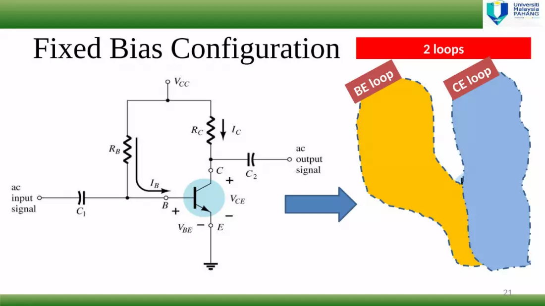
21
Fixed Bias Configuration 2 loops
BE loopCE loop

22
Fixed Bias ConfigurationDC equivalent circuit:1. BE loop
−𝑉 𝐶𝐶+ 𝐼𝐵𝑅𝐵+𝑉 𝐵𝐸=0
Write KVL equation
𝐼𝐵=𝑉 𝐶𝐶−𝑉 𝐵𝐸
𝑅𝐵

23
Fixed Bias ConfigurationDC equivalent circuit:2. CE loop
Write KVL equation
−𝑉 𝐶𝐶+ 𝐼𝐶 𝑅𝐶+𝑉 𝐶𝐸=0
𝐼𝐶=𝛽 𝐼𝐵

24
Fixed Bias ConfigurationDC equivalent circuit:
𝐼𝐵=𝑉 𝐶𝐶−𝑉 𝐵𝐸
𝑅𝐵
𝐼𝐶=𝛽 𝐼𝐵
Find RECALL:
𝑉 𝐶𝐸=𝑉 𝐶−𝑉 𝐸
𝑉 𝐵𝐸=𝑉 𝐵−𝑉 𝐸

25
Fixed Bias Configuration

26/133
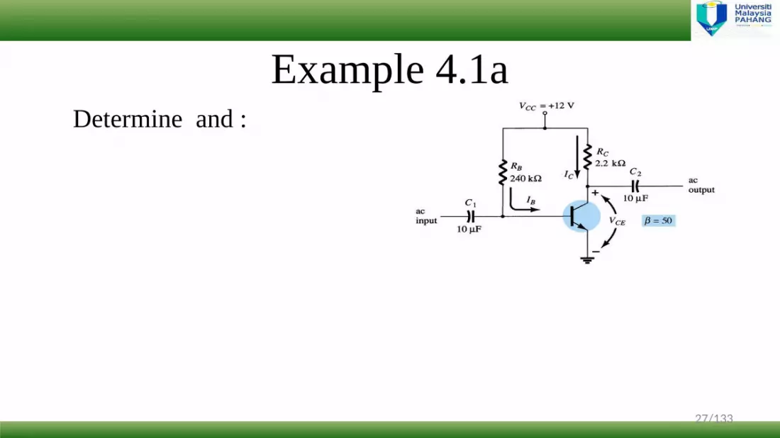
Example 4.1Determinea) and .b) c) and d)
47.08𝜇 𝐴 ,2.35𝑚𝐴 ,6.83𝑉 , 0.7𝑉 ,6.83𝑉 , −6.13𝑉
27/133
Example 4.1aDetermine and :

28/133
Example 4.1bDetermine :
𝐼𝐶=2.35𝑚
∴𝑉 𝐶𝐸𝑄=6.83𝑉

29/133
Example 4.1[c, d]Determine and :
𝑉 𝐵=0.7𝑉Determine :
83

30/133
Transistor Saturation
[𝑉 ¿¿𝐶𝐸 ,𝑉 𝐶𝐵 ]¿
• “Saturation”: reached their maximum value.• In transistor, saturation region is where the current
is in maximum value for the particular design.• Normally avoided:
– The BC junction is no longer reverse-biased – As a result, the output amplified signal will be distorted.

31/133
Transistor SaturationActual Approximate
Notice that in saturation region, 𝑉 𝐶𝐸=0
Applying Ohm’s law,
determine the
resistance between C
and E terminal,

32/133
Saturation LevelFor the fixed-bias configuration, to determine the saturation current, , the equivalent circuit is:
𝑉 𝐶𝐸=0𝑉 𝐶𝐸=𝑉 𝐶𝐶− 𝐼𝐶𝑅𝐶
𝑉 𝐶𝐸=𝑉 𝐶−𝑉 𝐸

33/133
Determine the saturation level for following circuit.
[5.45𝑚𝐴 ]
34/133
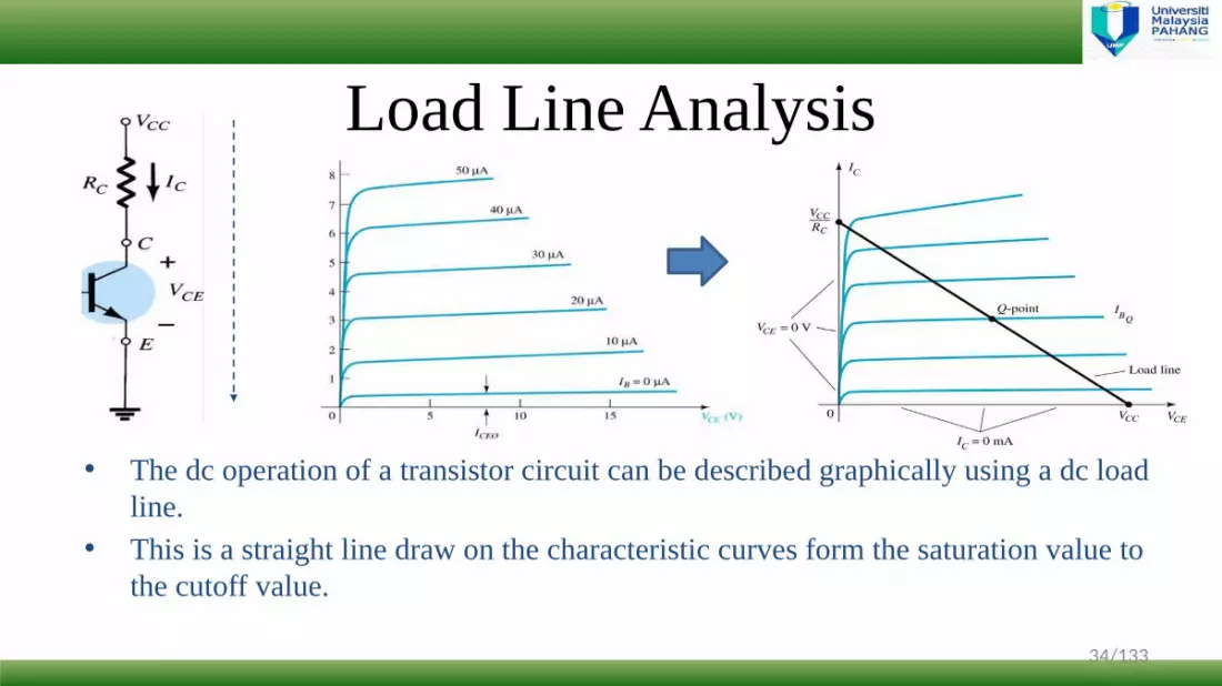
Load Line Analysis
• The dc operation of a transistor circuit can be described graphically using a dc load line.
• This is a straight line draw on the characteristic curves form the saturation value to the cutoff value.

35/133
Load Line Analysis

36/133
How to plot load line:
Load Line Analysis
Step 1: Find when
From , and
𝐼𝐶=𝑉 𝐶𝐶
𝑅𝐶

37/133
How to plot load line:
Load Line Analysis
Step 2: Find when
From , and
𝑉 𝐶𝐸=𝑉 𝐶𝐶

38/133
How to plot load line:
Load Line Analysis
Step 3: Draw straight line
𝑉 𝐶𝐸=𝑉 𝐶𝐶
𝐼𝐶=𝑉 𝐶𝐶
𝑅𝐶

39/133
Load-Line AnalysisThe characteristic becomes:
Q-point is establish from IB given

40/133
Load-Line AnalysisThe characteristic becomes:
??Increase or decrease of
𝑽 𝑪𝑪𝑰 𝑩 𝑹𝐂

41/133
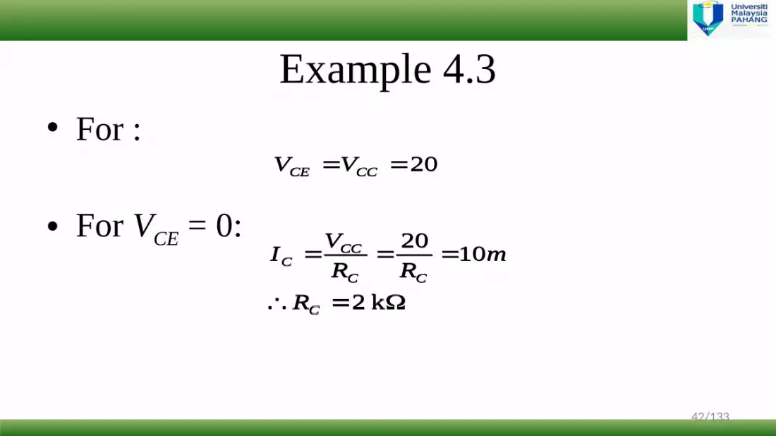
Example 4.3For fix biased, determine , and
𝑉 𝐶𝐶=𝑉 𝐶𝐸
𝐼𝐶=𝑉 𝐶𝐶
𝑅𝐶𝐼𝐵=?
42/133
Example 4.3• For :
• For VCE = 0:
20 CCCE VV
k 2
1020
C
CC
CCC
R
mRR
VI
20 CCCE VV
k 2
1020
C
CC
CCC
R
mRR
VI

43/133
Example 4.3• From the load-line given, Q-point is
approximately at • For a fixed-bias configuration, is defined by
the equation
• Since that , resulting in , can be calculated from the above equation:
𝐼𝐵=𝑉 𝐶𝐶−𝑉 𝐵
𝑅𝐵
=??

44/133
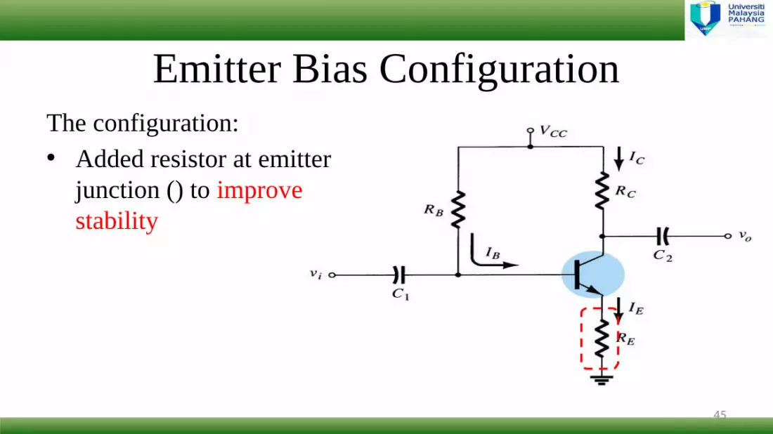
Emitter Bias Configuration
45
Emitter Bias ConfigurationThe configuration:• Added resistor at emitter
junction () to improve stability

46
Emitter Bias Configuration
+
-
𝑉 𝑅𝐵
+
-
𝑉 𝑅𝐶
+
+
-
𝑉 𝑅𝐸
+
-𝑉 𝐵𝐸
+
-𝑉 𝐶𝐸

47
Emitter Bias Configuration
+
-
𝑉 𝐵+
-
𝑉 𝐸
+
-
𝑉 𝐶

48
Emitter Bias Configuration
+
-
𝑉 𝑅𝐵
+
-
𝑉 𝑅𝐶
+
+
-
𝑉 𝑅𝐸
+
-𝑉 𝐵𝐸
+
-𝑉 𝐶𝐸+
-
𝑉 𝐵+
-
𝑉 𝐸
+
-
𝑉 𝐶

49/133
AnalysisB-E junction:+𝑉 𝐶𝐶 −𝑉 𝑅𝐵
−𝑉 𝐵𝐸−𝑉 𝑅𝐸=0
but
Thus
⋮
⋮
+𝑉 𝐶𝐶 − 𝐼𝐵𝑅𝐵−𝑉 𝐵𝐸− 𝐼𝐸𝑅𝐸=0

50/133
AnalysisC-E junction:
+𝑉 𝐶𝐶 −𝑉 𝑅𝐶−𝑉𝐶 𝐸−𝑉 𝑅𝐸
=0
Note: We can get
and from
+𝑉 𝐶𝐶 − 𝐼𝐶𝑅𝐶−𝑉 𝐶 𝐸− 𝐼𝐸𝑅𝐸=0
from

51/133
Example 4.4Determine for the emitter bias circuit below:

52/133
Example 4.4B-E junction:
𝑉 𝐵𝐸+¿ −𝑉 𝐸+¿−

53/133
Example 4.4
𝑉 𝐵𝐸+¿ − 𝑉 𝐸
𝑉 𝐶
+¿
−
𝑉 𝐶𝐸+¿−Thus,
– 2.046 .
C-E junction:

Example 4.4
𝑉 𝐵𝐸+¿ − 𝑉 𝐸
𝑉 𝐶
+¿
−
𝑉 𝐶𝐸+¿−
𝑰 𝑪=𝟐 .𝟎𝟏𝒎𝑨 , .
54
𝑰 𝑬=𝟐 .𝟎𝟒𝟔𝒎𝑨 ,
.
𝑽 𝑬=𝐼𝐸𝑅𝐸=2.046𝑚 (1𝑘 )=𝟐 .𝟎𝟒𝟔𝑽
𝑽 𝑩=𝑉 𝐶𝐶−𝑉 𝑅𝐵=20 − 𝐼𝐵𝑅𝐵=20 − 40.12𝜇 (430𝑘 )=𝟐 .𝟕𝟓𝑽
𝑉 𝐵𝐶=𝑉 𝐵−𝑉 𝐶=2.75 −15.98=13.23𝑉
,
15.98 V
𝑽 𝑩=𝑉 𝐵𝐸+𝑉 𝑅𝐸=𝑉 𝐵𝐸+𝐼 𝐸𝑅𝐸=0.7+2.046𝑚 (1𝑘 )=𝟐.𝟕𝟓𝑽
𝑉 𝐵
+¿
−

55/133
Example 4.4
𝑉 𝐵
+¿ 𝑉 𝐵𝐸+¿ − 𝑉 𝐸
𝑉 𝐶
+¿
− −
𝑉 𝐶𝐸+¿−
.
𝑉 𝐸=51 𝐼𝐵=51 (40.12𝜇)=2.05𝑉𝑉 𝐵=20 − (430𝑘 ) 𝐼𝐵=2.75𝑉𝑉 𝐶𝐸=𝑉 𝐶−𝑉 𝐸=15.98 − 2.05=13.93𝑉𝑉 𝐵𝐶=𝑉 𝐵−𝑉 𝐶=2.75 −15.98=−13.23𝑉
C-E junction:

56/133
Improve bias stability?Prepare a table and compare the bias voltage and current of the both circuits for the given value and a new value of . Compare the changes in and for the same increasing in

57/133
β
β
Fixed-bias
Emitter-bias

58
Saturation LevelFor the emitter-bias configuration, to determine the saturation current, , the equivalent circuit is:
𝐼𝐶=𝑉 𝐶𝐶
𝑅𝐶+𝑅𝐸𝐼𝐶≈ 𝐼𝐸

59/133
Load-Line Analysis• For , the transistor will be in saturation region• Taking the transistor saturation equation:
• For :

60
Load-Line Analysis• So, the load-line becomes:

61
Voltage Divider Bias Configuration

62
Voltage-Divider Bias Configuration• The configuration:• Added R2 for RB connected to
ground• Two kind of analysis for voltage-
divider bias:– Exact Analysis– Approximate Analysis

63/133
Exact Analysis• Thevenin equivalent circuit is applied for , ground, and at
base terminal • The circuit at base terminal becomes:

64/133
Exact Analysisand must be determined for Thevenin equivalent circuit
Determining RTH - Determining ETH

65/133
Exact Analysis• The Thevenin equivalent circuit at base
terminal becomes:

66/133
Example 4.7• Determine VCE and IC

67/133
Example 4.7• Determining RTH:
• Determining ETH (by applying nodal analysis at base terminal):
k 55.39.339
)9.3)(39(
21
2121 kk
kkRR
RRRRRTH
V 29.339
2221
TH
THTH
THTHCC
Ek
EkE
RE
REV
k 55.39.339
)9.3)(39(
21
2121 kk
kkRR
RRRRRTH
V 29.339
2221
TH
THTH
THTHCC
Ek
EkE
RE
REV

68/133
Example 4.7Then applied the same technique as in fixed-bias or emitter-bias configuration to get the value of IB:
– Reference at B-E junction where VBE = 0.7 V
– Develop an equation for VB:
– Then, develop an equation for VE:
V 7.0 EBBE VVV
BB
B
TH
BTHB
kIVk
VR
VEI
55.3255.3
2
BE
E
E
EBE
kIVk
VRVII
5.2115.1
1
V 7.0 EBBE VVV
BB
B
TH
BTHB
kIVk
VR
VEI
55.3255.3
2
BE
E
E
EBE
kIVk
VRVII
5.2115.1
1

69/133
Example 4.7– From VB and VE, insert to equation VBE:
– For IC:
– Get VC from IC equation:
A 05.65.21155.327.0
B
BBBE
IkIkIV
mA 85.005.6140 BC II
V 5.13 10
2285.0
CC
C
CCCC
VkVm
RVVI
A 05.65.21155.327.0
B
BBBE
IkIkIV
mA 85.005.6140 BC II
V 5.13 10
2285.0
CC
C
CCCC
VkVm
RVVI

70/133
Example 4.7– For the value of VE, insert the value of IB into the VE
equation:
– For VCE:
V 28.1)05.6(5.2115.211 kkIV BE
V 22.1228.15.13 ECCE VVV
V 28.1)05.6(5.2115.211 kkIV BE
V 22.1228.15.13 ECCE VVV

71/133
The Approximate Analysis• For approximate analysis, we can assume:
• But the below condition must be satisfied so that the approximate analysis can be done:
BTH VE
210RRE
BTH VE
210RRE

72/133
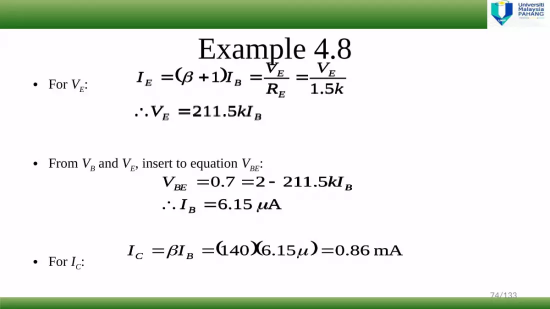
Example 4.8• Repeat Example 4.7 using the approximate analysis technique
and compare the solutions for IC and VCE

73/133
Example 4.8• Examine the condition for the approximate analysis technique:
• So the equation βRE ≥ 10R2 is satisfied resulting in ETH = VB
• By applying nodal analysis at node ETH:
39000)9.3)(10(10210000)5.1)(140(
2
kRkRE
V 29.339
2221
B
BB
BBCC
Vk
VkV
RV
RVV
39000)9.3)(10(10210000)5.1)(140(
2
kRkRE
V 29.339
2221
B
BB
BBCC
Vk
VkV
RV
RVV
74/133
Example 4.8• For VE:
• From VB and VE, insert to equation VBE:
• For IC:
BE
E
E
EBE
kIVk
VRVII
5.2115.1
1
A 15.65.21127.0
B
BBE
IkIV
mA 86.015.6140 BC II
BE
E
E
EBE
kIVk
VRVII
5.2115.1
1
A 15.65.21127.0
B
BBE
IkIV
mA 86.015.6140 BC II

75/133
Example 4.8• For VC:
• For the value of VE, insert the value of IB into the VE equation:
• For VCE:
V 4.1310
2286.0
C
C
C
CCCC
VkVm
RVVI
V 3.1)15.6(5.2115.211 kkIV BE
V 1.123.14.13 ECCE VVV
V 4.1310
2286.0
C
C
C
CCCC
VkVm
RVVI
V 3.1)15.6(5.2115.211 kkIV BE
V 1.123.14.13 ECCE VVV

76/133
Example 4.8• By comparing the result from exact analysis with approximate
analysis:
• The approximate value of Ic and VCE is acceptable due to only small difference between them
IC (mA) VCE (V)
Exact Analysis 0.85 12.22
Approximate Analysis 0.86 12.1
77/133
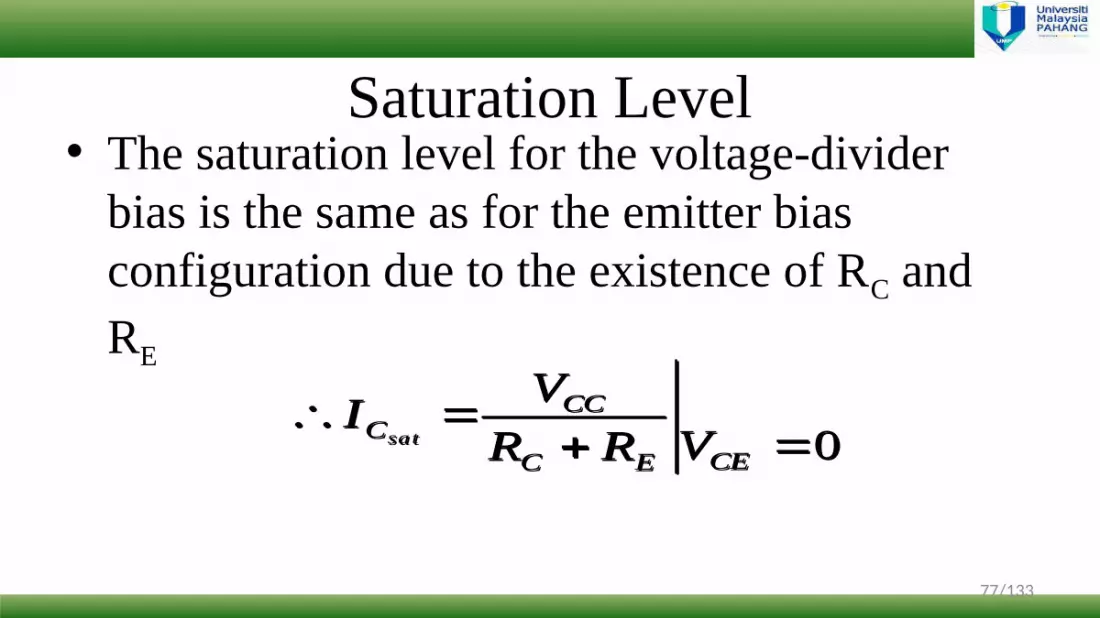
Saturation Level• The saturation level for the voltage-divider
bias is the same as for the emitter bias configuration due to the existence of RC and RE
0
CEEC
CCC VRR
VIsa t 0
CEEC
CCC VRR
VIsat

78/133
Load Line Analysis• As for the load-line analysis, the cutoff region still
resulting in the same result as the fixed bias and emitter bias configuration:
• And for the saturation region:
0CICCCE VV
0
CEEC
CCC VRR
VIsat
0CICCCE VV
0
CEEC
CCC VRR
VIsat

79
DC Bias Voltage Feedback Configuration

80/133
DC Bias with Voltage Feedback• The base resistor (RB) is connected to VC instead of VCC
• The configuration:

81/133
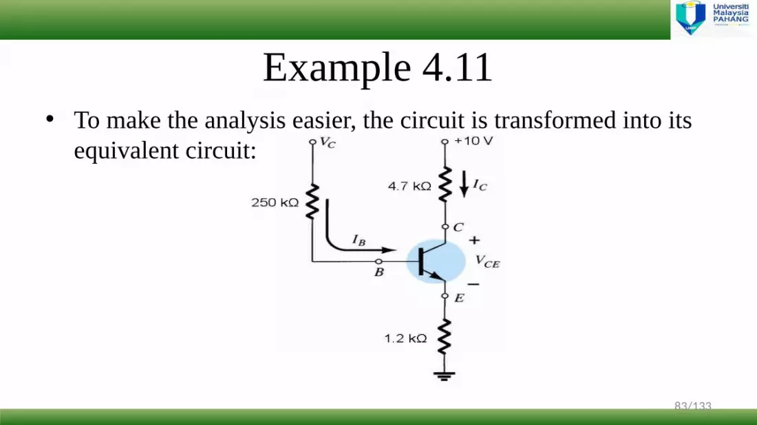
Example 4.11
𝑹𝑩𝑹𝑪
𝑹𝑬
𝑽 𝑪𝑪𝑽 𝑪𝑪

82/133
Example 4.11• Determine IC and VCE
83/133
Example 4.11• To make the analysis easier, the circuit is transformed into its
equivalent circuit:

84/133
Example 4.11• For VB:
• Because of the existence of VC, the equation of VC has to be obtained
• Insert the VC equation into the VB equation:
• For VE:
BCB
BCB
kIVVkVVI
250250
BC
cBC
kIVkVII
423107.4
10
BBBB kIkIkIV 6731025042310
BE
EBE
kIVk
VII
2.1092.1
1
BCB
BCB
kIVVkVVI
250250
BC
cBC
kIVkVII
423107.4
10
BBBB kIkIkIV 6731025042310
BE
EBE
kIVk
VII
2.1092.1
1

85/133
Example 4.11• By substituting the VBE equation:
• By applying the same technique as in other bias configuration that has been explained before to get IC and VCE:
A 89.112.109673107.0
B
BBBE
IkIkIV
V 67.3mA 07.1
CE
C
VI
A 89.112.109673107.0
B
BBBE
IkIkIV
V 67.3mA 07.1
CE
C
VI

86/133
Miscellaneous Bias Configurations
• There are many types of bias configuration other than the four that have been explained
• The calculation technique applied is the same for all BJT configuration, start with VBE = 0.7 V because it is fixed for all npn transistor (VEB = 0.7 V for pnp transistor)
• Once the base current (IB) is obtained, all other current and voltage can be calculated
• In the examples provided in this subtopics, the calculation shown only to obtained IB and all the other value can be calculated by applying the technique that have been explained before

87/133
Example 4.14• The circuit:

88/133
Example 4.14• The calculation:
BCB
BCB
BC
CBC
kIVVkVVI
kIVkVII
680680
564207.4
20
A 51.1501244207.0
0
12442068056420
B
BEBBE
E
BB
BBB
IkIVVV
V
kIVkIkIV
BCB
BCB
BC
CBC
kIVVkVVI
kIVkVII
680680
564207.4
20
A 51.1501244207.0
0
12442068056420
B
BEBBE
E
BB
BBB
IkIVVV
V
kIVkIkIV

89/133
Example 4.15• The circuit:

90/133
Example 4.15• The calculation:
A 83)9(1007.0
9
1001000
B
BBE
E
BB
BB
IkIV
V
kIVk
VI
A 83)9(1007.0
9
1001000
B
BBE
E
BB
BB
IkIV
V
kIVk
VI

91/133
Example 4.16• The circuit:

92/133
Example 4.16• The calculation:
A 73.45
201822407.0
201822
)20()1(
2402400
B
BBEBBE
BE
EBE
BB
BB
IkIkIVVV
kIVk
VII
kIVk
VI
A 73.45
201822407.0
201822
)20()1(
2402400
B
BBEBBE
BE
EBE
BB
BB
IkIkIVVV
kIVk
VII
kIVk
VI

93/133
Example 4.17• The circuit:

94/133
Example 4.17• The calculation:
A 08.45
42.7307.0
42.732.1
)4()1(
0
B
BBE
BE
EBE
B
IkIV
kIVk
VII
V
A 08.45
42.7307.0
42.732.1
)4()1(
0
B
BBE
BE
EBE
B
IkIV
kIVk
VII
V

95/133
Example 4.18• The circuit:

96/133
Example 4.18• The calculation:
BB
B
TH
BTHB
TH
THTH
TH
kIVk
VR
VEI
Ek
EkE
kkkkR
73.154.1173.154.11
V 54.112.2
)20(2.8
20
k 73.12.22.8
)2.2)(2.8(
A 35.35
208.21773.154.117.0
208.2178.1
)20()1(
B
BB
BE
BE
EBE
IkIkI
V
kIVk
VII
BB
B
TH
BTHB
TH
THTH
TH
kIVk
VR
VEI
Ek
EkE
kkkkR
73.154.1173.154.11
V 54.112.2
)20(2.8
20
k 73.12.22.8
)2.2)(2.8(
A 35.35
208.21773.154.117.0
208.2178.1
)20()1(
B
BB
BE
BE
EBE
IkIkI
V
kIVk
VII

97/133
Bias Stabilization
Fixed-bias β dependent not stable
Emitter-bias stabilization increase still β dependent
Voltage-dividerbias β independent stabilize
DC bias withvoltage feedback stabilization increase due to feedback of RB less β dependent

98/133
Design Operation• All the technique that has been explained previously in
this topic are used for circuit analysis where the current and voltage are calculated and obtained.
• In design operation, some of the current and voltage are given meanwhile the value of the resistors have to be obtained in order to design the required bias configuration (all the techniques still applied).
• Only one assumption has to be made in design operation that is:
CCE VV101
CCE VV101

99/133
Example 4.22• Determine all resistors value in designing an emitter-bias
configuration

100/133
Example 4.22According to the design operation assumption:
From the given value:
To obtain :
𝑉 𝐸=1
10𝑉 𝐶𝐶=110
(20 )=2𝑉
101/133
Example 4.22Due to , is obtained:
Due to , is obtained:
V

102/133
Once the theoretical values of the resistors are determined, • the nearest standard
commercial values are normally chosen and
• any variations due to not using the exact resistance values are accepted as part of the design.
RC
RE
RB

103/133
Example 4.23Determine the all resistors value in designing a voltage-divider bias
configuration

104/133
Example 4.23• According to the design operation assumption:
• From the VCE value given:
• To obtain RC:
V 2)20(101
101
CCE VV
V 1028
C
CECCE
VVVVV
k 1
102010
C
C
C
CCCC
RR
m
RVVI
V 2)20(101
101
CCE VV
V 1028
C
CECCE
VVVVV
k 1
102010
C
C
C
CCCC
RR
m
RVVI

105/133
Example 4.22• Applying nodal analysis at node VB to obtain the value of R1:
• Note that the value obtained is recommended using 10 kΩ due to 10.25 kΩ is not exist in the real world
)k 10 (use k 25.106.17.27.220
1
1
RkR
)k 10 (use k 25.106.17.27.220
1
1
RkR

106/133
Transistor Switching Networks• Transistor also can be used as switches for computer
applications• One of the example in computer application is the transistor
usage as an inverter• The circuit:

107/133
Transistor Switching Networks• Examine the circuit to obtained the load-line analysis point at
cutoff and saturation region
• The transistor will work in the cutoff region and saturation region, as for that 2 Q-point will be achieved
region)n (saturatiomA 6.182.05
region)-(cutoff V 5 0
kRVI
VV
C
CCC
ICCCE
sat
C
region)n (saturatiomA 6.182.05
region)-(cutoff V 5 0
kRVI
VV
C
CCC
ICCCE
sat
C

108/133
Transistor Switching Networks• The load-line analysis will become:

109/133
Transistor Switching Networks• Because of VE is grounded, so VBE = VB = 0.7• For vin = 0:
• IB = -10.29 μA is way below IB = 0 A in the load-line, so for sure it is in the cutoff-region
• Because of VCE = VCC for cutoff-region, while VC = VCE for this configuration, the output VC will be 5 V
• For vin = 5:
• IB = 63.24 μA is way above IB = 50 μ A in the load-line, so for sure it is in the saturation-region
• Because of VCE = 0 for saturation-region, while VC = VCE for this configuration, the output VC will be 0 V
A 29.1068
7.00
kR
VVIB
BiB
A 24.6368
7.05
kR
VVIB
BiB
A 29.1068
7.00
kR
VVIB
BiB
A 24.6368
7.05
kR
VVIB
BiB

110/133
Example 4.24• Determine RB and RC for the transistor inverter if ICsat = 10 mA

111/133
Example 4.24• At the saturation point, ICsat is defined by:
• Obtaining IB for saturation region:
k 1
1010
C
C
C
CCC
RR
m
RVI
sat
μA 4025010
B
B
BC
IIm
IIsat
k 1
1010
C
C
C
CCC
RR
m
RVI
sat
μA 4025010
B
B
BC
IIm
IIsa t

112/133
Example 4.24• To make sure that IB is really in the saturation region, use IB
greater than the IB obtained at the saturation point. As for that, use IB = 60 μA
• At saturation region, input voltage Vi must be high. As for that, Vi = 10 V
• Because VE = 0 and VBE = 0.7, the value of VB = 0.7• To obtain RB:
)k 150 (use k 155
7.01060
B
B
B
BiB
RR
RVVI
)k 150 (use k 155
7.01060
B
B
B
BiB
RR
RVVI

113/133
Example 4.24• Use 150 kΩ due to 155 kΩ is not exist in the real world• Check back whether 150 kΩ can be used for transistor switching
network:
• The saturation point is at IB = 40 μA, so the use of 150 kΩ is appropriate because the IB produced is surely in the saturation region
A 62150
7.010
kR
VVIB
BiB A 62
1507.010
kRVVI
B
BiB

114/133
pnp Transistors• Note that all the analysis and techniques explained is only
involving npn transistors.
• Therefore for pnp transistor, all of the analysis and techniques learned can also be applied because of the total current flowing in and out of the transistor is still the same as in npn that is IE = IB + IC
• The only difference between npn and pnp transistor is the direction of the current flows in and out of the transistor

115/133
Example 4.27• Obtain VCE

116/133
Example 4.27• By examining the circuit given, it is a voltage-divider bias
configuration• As for that, approximate analysis can be done if the condition
are satisfied:
• The condition are satisfied, approximate analysis can be used:
2
2
10k 100)10(1010
k 132)1.1)(120(
RRkR
kR
E
E
BTH VE
2
2
10k 100)10(1010
k 132)1.1)(120(
RRkR
kR
E
E
BTH VE
117/133
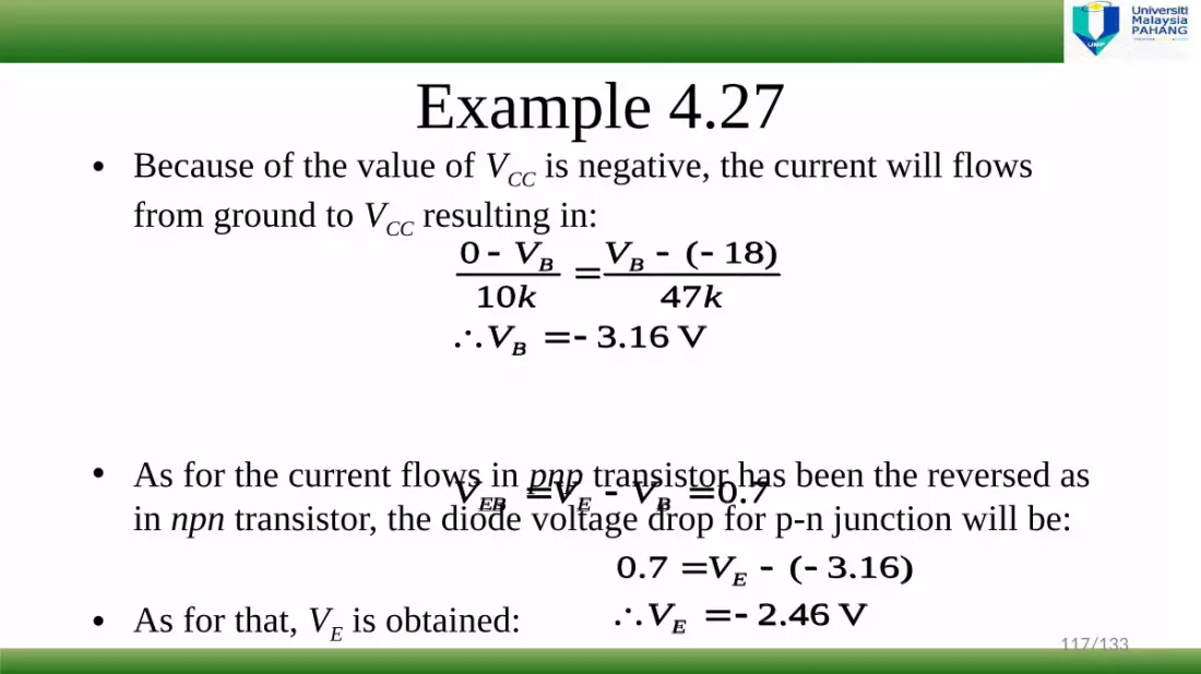
Example 4.27• Because of the value of VCC is negative, the current will flows
from ground to VCC resulting in:
• As for the current flows in pnp transistor has been the reversed as in npn transistor, the diode voltage drop for p-n junction will be:
• As for that, VE is obtained:
V 16.347
)18(10
0
B
BB
Vk
VkV
7.0 BEEB VVV
V 46.2)16.3(7.0
E
E
VV
V 16.347
)18(10
0
B
BB
Vk
VkV
7.0 BEEB VVV
V 46.2)16.3(7.0
E
E
VV

118/133
Example 4.27• For IE:
• As for IC ≈ IE, VC is obtained:
mA 24.21.1
)46.2(1.1
0
kkVI E
E
V 62.124.2
)18(mA 24.2
C
C
C
CCCC
Vk
VR
VVI
mA 24.21.1
)46.2(1.1
0
kkVI E
E
V 62.124.2
)18(mA 24.2
C
C
C
CCCC
Vk
VR
VVI

119/133
Example 4.27• Finally, VCE is obtained:
V 16.10)46.2(62.12 ECCE VVV V 16.10)46.2(62.12 ECCE VVV

120/133
Transistor Hints and Tips• All the transistor current (IB, IC and IE) must be
in positive values due to the current flows in and out of the transistor must be satisfied, IE = IB + IC
• The base current IB must be small (in μA) to ensure that the equation IC ≈ IE is satisfied


