Embed Size (px)
Citation preview

Ds
Da
b
a
ARRAA
KSSSH
1
btosoImripadtvatbsi
0h
Applied Surface Science 299 (2014) 6–11
Contents lists available at ScienceDirect
Applied Surface Science
journa l h om epa ge: www.elsev ier .com/ locate /apsusc
ouble layer SiO2/Al2O3 high emissivity coatings on stainless steelubstrates using simple spray deposition system
.B. Mahadika, Sharath Gujjara, Girish M. Goudab, Harish C. Barshiliaa,∗
Nanomaterials Research Laboratory, Surface Engineering Division CSIR-National Aerospace Laboratories, Bangalore 560017, IndiaLaboratory for Electro-Optics Systems, Indian Space Research Organization (ISRO), Bangalore 560058, India
r t i c l e i n f o
rticle history:eceived 24 October 2013eceived in revised form 24 January 2014ccepted 25 January 2014vailable online 2 February 2014
eywords:
a b s t r a c t
High emissivity coatings (ε > 0.90) are widely used in spacecraft and industrial furnaces, which haveattracted a great attention recently due to energy saving applications. In this study, a simple spray coat-ing method was used to produce double layer high emissivity coatings on stainless steel (SS) substrateby sol–gel process at room temperature. Initially, silica (SiO2), sol prepared using sol–gel process, wasdeposited on sandblasted SS substrate with required thickness, followed by deposition of aluminiumoxide (Al2O3) layer. The gradual increase in the thickness of Al2O3 layer resulted in increase in the emit-
ol–gelpray deposition systemiO2/Al2O3 coatingigh emissivity
tance. The optimized double layer Al2O3 (23.0 �m)/SiO2 (9.13 �m) coating on SS substrate exhibitedhigh emittance (ε = 0.92–0.94) and low absorptance ( ̨ = 0.30–0.34). The high emissivity coating, whenexposed to a temperature of 1000 ◦C in air got crystallized but retained its optical properties. For exam-ple, the heat-treated coating exhibited an emittance of 0.92 (measured at 82 ◦C) and absorptance of 0.42.The SiO2/Al2O3 coating, thus, provides a simple and cost effective method for the preparation of highemissivity coatings.
. Introduction
The emissivity (ε) of a material is the ratio of energy radiatedy the material to energy radiated by a blackbody at the sameemperature. A perfect blackbody exhibits ε = 1, whereas, any realbject exhibits ε < 1. For example, a highly polished copper blockhows emissivity of the order of 0.02–0.03. On the other hand, mostf the non-transparent insulators exhibit emissivity up to 0.80.n general, materials with ε > 0.90 are known as high emissivity
aterials. High emissivity coatings have received a great attentionecently, especially for spacecraft applications [1,2], radiative cool-ng applications [3] and electrical insulation [4]. These coatingsrovide enhanced radiant heat transfer from refractory surfaces,llowing a substantial reduction in energy costs and emissions inirect-fired furnaces [5,6]. The solar cells on spacecraft are exposedo very harsh thermal environment during friction between spaceehicle surface and atmosphere, which seriously affect the lifetimend performance of solar cells on the spacecrafts [7,8]. Therefore,hermal radiative properties of surface coatings are important
ecause as the temperature increases, conversion efficiency of theolar cells and life time of material decreases. Hence, high emissiv-ty coating is deposited on the spacecrafts to decrease the surface∗ Corresponding author. Tel.: +91 80 2508 6494; fax: +91 80 2521 0113.E-mail address: [email protected] (H.C. Barshilia).
169-4332/$ – see front matter © 2014 Elsevier B.V. All rights reserved.ttp://dx.doi.org/10.1016/j.apsusc.2014.01.159
© 2014 Elsevier B.V. All rights reserved.
temperature by the radiation. These coatings effectively transferheat by radiation [9]. Similarly, applying a high emissivity coatingon the furnace wall increases the net temperature in the interior ofthe furnace, which ultimately helps to save electric power [10,11].Shioya et al. [12] reported 13% energy saving in fuel consumption,after application of high emissivity (0.90) coating inside thefurnace.
Emittance is an important material property that enables deter-mining the emissive power of a real body. The emittance dependson the reflectance (R) and transmittance (�) of the material, which,in turn, depends on temperature (T) of the material and wave-length (�) of the radiation. According to Kirchhoff’s law for perfectlyopaque bodies ε = 1 − R. The emittance here is characterized todescribe the surface radiative property which involves the transferof heat by electromagnetic radiation arising due to the tempera-ture of a body. The total normal emissivity at room temperature, iscalculated by integrating spectral reflectance in the spectral regionof 2.5–25 �m wavelength and is expressed as [3,12]:
ε(T) =∫ 25
2.5{1 − R(�, � = 0)}ib(�, T)d�
∫ 252.5
ib(�, T)d�, (1)
where, � is incident angle, ib(�,T) is the spectral intensity of ablackbody at temperature T. This spectral region includes emissivepower of a body at room temperature. Hence low reflectance in farinfrared region centered around 10 �m produces high emissivity

Surfa
ai
fabti[apbtpetshncie[estmhhs[
ofitappiTossPih
eSTltwtsstaeeaStaae
D.B. Mahadik et al. / Applied
t room temperature. The emissivity study in this spectral regions usually used for thermal design of spacecraft [13].
In the literature, many high emissivity coatings are reportedor thermal protection of solar cells, spacecrafts and energy savingpplication for industrial furnace to lower the surface temperaturey various deposition methods. Kazomori et al. [1] have reportedhat the emissivity increases to 0.77 by applying SiO2/Al2O3 coat-ng on solar cell thin films by e-beam evaporation. Tang et al.14,15] have reported coatings by micro-arc oxidation of titaniumlloy, which shows high emissivity of 0.90. Jianping et al. [7] haverepared the cauliflower like microstructured CeO2 coatings by e-eam evaporation, which show an emissivity of 0.90 at 873 K inhe mid-infrared spectral range. Some authors have used sol–gelrocess for the synthesis of high emissivity coatings on differ-nt substrates. For example, Zhao et al. [8] have reported thathe carbon nanotubes doped SiO2/SiO2–PbO double layer coatingshow high emissivity of 0.94. Similarly, Chelashaw et al. [16]ave reported high emissivity (0.91–0.94) by dispersing ceramicano-particles in Al2O3 sol matrices, prepared by sol–gel sprayoating method. Holcombe et al. [17] have applied high emissiv-ty coating for coating the interior of a furnace to direct thermalnergy toward a load in the furnace. Similarly, Heynderickx et al.18] reported 5% increase in the performance by applying highmissivity coating on the pyrolysis furnace. Various techniquesuch as chemical vapor deposition and physical vapor deposi-ion have been used to deposit high emissivity coatings. However,
ost of these methods are costly and require vacuum, targets ofigh purity and high processing temperature. Therefore, attemptsave been made to develop high emissivity coatings by simpleol–gel process at room temperature using spray deposition system8,16].
In recent years, sol–gel method has been receiving a great dealf attention among the scientists and engineers working in theeld of nanomaterials due to the relative ease and reliability ofhe sol–gel method in the synthesis and processing of nanomateri-ls with high degree of purity. The other advantages of the sol–gelrocessing are the cost reduction, made possible by the low tem-eratures involved, porosity control, and relatively less expensive
nstrumentation and techniques required for the synthesis [19,20].hough, there are a variety of methods available for the depositionf high emissivity coatings, simple and cost effective processes likepray or dip coating method could be used to deposit films on sub-trates of arbitrary shape, and is easily adaptable to industrial scale.orous structure, which is expected to improve coating’s emissiv-ty by creating much more reflecting interfaces [21], is prepared byybrid sol–gel method.
The motivation to select two different layers to achieve highmittance in the present work is as follows. It is well known thatiO2 shows high emissivity (∼0.84) in the mid infrared region.o develop high emissivity and low absorptance coating secondayer of Al2O3 was deposited due to its suitable optical proper-ies, i.e., low extinction coefficient and low absorptance in theavelength region 2.5–25 �m. Accordingly, this paper presents
he development of high emissivity coating of SiO2/Al2O3 onandblasted stainless steel (SS) substrate using spray depositionystem. First, thickness of SiO2 layer was optimized and thenhickness of Al2O3 layer was optimized to achieve high emittancend low absorptance coating. For the optimized process param-ters, (i.e., sol–gel parameters, thickness, annealing temperature,tc.) high emittance value (0.94) in the infrared region and lowbsorptance (0.30) in the visible region have been achieved for thisiO2/Al2O3 coating. Several characterization techniques were used
o study the optical properties and structural characteristics of thes-prepared SiO2/Al2O3 coatings. Solar spectrum reflectometernd emissometer were used to measure the absorptance andmittance of the coating, respectively. Fourier transform infraredce Science 299 (2014) 6–11 7
(FTIR) spectrometer was used to determine the reflectance spectrain the 2.5–25 �m wavelength region. X-ray diffraction (XRD), 3Dprofilometer, X-ray photoelectron spectroscopy (XPS) and fieldemission scanning electron microscopy (FESEM) were used tostudy the structural, microstructural and chemical characteristicsof the high emissivity coatings. To check the thermal stabilityof SiO2/Al2O3 high emissivity coatings, heat treatment of theoptimized sample has been carried out in air for 2 h at 1000 ◦C. Anickel based superalloy substrate was used for these studies.
2. Experimental details
The samples were prepared on sand-blasted stainless steel sub-strates. In sand blasting process, a smooth surface is converted intoa rough surface to enhance the emissivity and adhesion of the coat-ing material. The sand blasting has been carried out for about 3 min,which induces a root mean square roughness (�) of ∼2.9 �m. It maybe noted that sandblasted bare SS substrates showed an emittanceof 0.63 and an absorptance of 0.45. Thus, prepared rough samplesof stainless steel were cleaned and used for the deposition of SiO2and Al2O3 coatings.
For the preparation of coating sol the following chemicalswere used: tetraethylorthosilicate (TEOS), (3-glycidyloxypropyl)trimethoxysilane (GPTMS) and aluminum tri-sec-butoxide (Al(O-sec-Bu)3) (Sigma–Aldrich Chemie, Germany), ethanol, ethylacetoacetate and isopropyl alcohol (i-PrOH) (S.D. Fine Chem, Ltd.).Milli-Q water was used for the preparation of diluted hydrochlo-ric and acetic acid catalysts. The SiO2 sol was prepared usingTEOS diluted in ethanol. Acidic water in the form of hydrochlo-ric acid (0.001 M HCl) was added to this solution and continuouslymagnetically stirred for 24 h at room temperature for completehydrolysis [22]. The molar ratio of TEOS:EtOH:H2O was 1:40:2,respectively. The resulted sol was used for the deposition after24 h aging at room temperature. Al(O-sec-Bu)3 and isopropyl alco-hol were mixed and magnetically stirred at room temperature for1 h. Ethyl acetoacetate was added to the solution as a chelatingagent to control the rate of reaction and solution was contin-uously magnetically stirred for 24 h [23]. After stirring, waterdiluted with i-PrOH was carefully added drop wise to the solu-tion for hydrolysis and continued stirring for 2 h. The molar ratiosof i-PrOH, EAcAc, and H2O to Al(O-sec-Bu)3 were 20, 1 and 2,respectively.
In order to improve the adhesion of Al2O3 coating a binder solhaving GPTMS and TEOS in molar ratio 1:1 with ethanol solventand 1 M acetic acid catalyst were used. Ethanol and water to silaneratio was 11 and 2, respectively. The sol was magnetically stirredfor 24 h for complete hydrolysis. This sol was added to Al2O3 soland magnetically stirred for 5 h to mix thoroughly in Al2O3 sol andfinally used for the deposition.
First, SiO2 layer was deposited on sand-blasted stainless steelsubstrate using simple spray coating process at room tempera-ture. The air pressure of the spray deposition system was keptat 0.5 bar and the number of passes (4, 6, 8 and 10) of spray gunof SiO2 sol were used to get different thicknesses (2.2, 6.21, 9.13and 13.4 �m). After deposition of SiO2 layer, the substrates weredried at 100 ◦C in air atmosphere for 1 h for densification of thenetwork and evaporation of the solvent. Al2O3 layer with differ-ent thicknesses were deposited on top of SiO2 layer coated on SSsubstrates. These samples were further annealed in air at 100 ◦Cfor 1 h. In order to measure the thickness of the coatings, SiO2 andAl2O3 layers were deposited on half-masked polished Si substrates.
The masked was removed after deposition. The step thus formedwas used to measure the thickness of the coatings using a 3-D pro-filometer (NanoMap). The schematic model of SiO2/Al2O3 doublelayer high emissivity coating is shown in Fig. 1.
8 D.B. Mahadik et al. / Applied Surface Science 299 (2014) 6–11
Fd
waadawowtrdwrrsaosXt(rcrT(bCtoae
3
3
w
Fc
2421181512963
0.89
0.90
0.91
0.92
0.93
0.94
Thickness (µµm)
Em
itta
nce
Emittance
0.30
0.35
0.40
0.45
0.50
0.55
0.60
Ab
sorp
tan
ce
Absorpta nce
ig. 1. Schematic diagram of SiO2/Al2O3 double layer high emissivity coatingeposited on sandblasted stainless steel substrate.
The absorptance and emittance of the high emissivity coatingsere measured using solar spectrum reflectometer (Model SSR)
nd emissometer (Model AE) of M/s. Devices and Services. Thebsorptance and the emittance values were measured at threeifferent positions and the values reported herein are the aver-ge of four measurements. The emissometer was heated to 82 ◦C,hich is a special purpose instrument to measure the emittance
f absorber coatings used for flat plate solar thermal collector,herein the maximum working temperature of the collector is of
he order of 80–85 ◦C. At 82 ◦C, the spectral range of the thermaladiation emitted from the surface is in the range of 3–30 �m. Theetector in the emissometer consists of a differential thermopileith low and high emittance areas, which ensures near constant
esponse to the emitted radiation in this wavelength range. Theeflectometer and emissometer were calibrated using standardamples. The accuracies of the measured � values are ±0.02 with
drift of ±0.01 + 0.003 /h and the emissometer has a repeatabilityf ±0.01 units. Reflectance spectra of the samples were also mea-ured using Spectrum GX FTIR spectrometer from PerkinElmer. TheRD patterns of the coatings were recorded using X-ray diffrac-
ometer (Bruker D8) having thin film attachment. Cu K� radiation� = 0.154 nm), operated at 40 kV and 40 mA, was used as the X-ay source. The microstructural and morphological details of theoatings were investigated using Supra 40 VP, Carl Zeiss high-esolution field emission scanning electron microscopy (FESEM).he bonding structure of the coatings was characterized by XPSSPECS) using non-monochromatic Al K� radiation (1486.8 eV). Theinding energies reported here were calculated with reference to1s peak at 284.6 eV with a precision of 0.1 eV. In order to test thehermal stability, SiO2/Al2O3 high emissivity coatings, depositedn superalloy substrates, were heated in air fired tubular furnacet 1000 ◦C temperature for 2 h. Changes in the absorptance andmittance of the samples after heat treatment were studied.
. 3 Results and discussion
.1. Single/double layer SiO2 and Al2O3 coatings
Cleaned stainless steel substrates after sand blasting processere used to deposit SiO2 coating by spray deposition method.
1412108642
0.82
0.84
0.86
0.88
0.90
Ab
sorp
tan
ce
Absorptance
Emitta nce
Em
itta
nce
Thickness (µµm)
0.60
0.65
0.70
0.75
0.80
0.85
ig. 2. Plots of emittance and absorptance versus thickness of single layer SiO2
oatings.
Fig. 3. Plots of emittance and absorptance versus thickness of Al2O3 coating on9.13 �m thick SiO2 layer deposited on sandblasted SS substrates.
Fig. 2 shows the variations of emittance and absorptance valueswith thickness of SiO2 coating. It is observed that as thicknessincreases the emittance increases from 0.82 to 0.89 with nearlyconstant absorptance values of 0.77–0.78. The enhancement ofemissivity by increasing SiO2 thickness is therefore limited. It maybe noted that at coating thickness greater than 13 �m, SiO2 coatingsexhibited large cracks presumably because of increased stress level.Therefore, SiO2 coating thickness of 9.2 �m was used for furtherdeposition of the second layer.
When the radiation falls on a body, it may be partially reflected,transmitted or absorbed. The light penetration depth ‘dp’ is closelyrelated to the emissivity of coating, which in turn depends on thewavelength (�) of the light and the extinction coefficient (k) [3],
dp = 1˛
= �
4�k· (2)
This equation suggests that k should be as low as possible toincrease the penetration depth. Therefore, a material which hashigh penetration depth is required to achieve high emissivity. SiO2has a low extinction coefficient, and single layer of SiO2 itselfshowed maximum high emittance up to 0.84 with good adhesionwith SS substrate but absorptance of this layer was high (0.78).Al2O3 is a well known material with very low extinction coeffi-cient [24]. Therefore, a thick layer of Al2O3 material was selectedfor the deposition of second layer on the SiO2 coated SS substrateto decrease the absorptance of SiO2 coating and increase the emit-tance. The variations of emittance and absorptance with respectto thickness of Al2O3 coating on SiO2 coated samples are shownin Fig. 3. With increasing thickness of Al2O3 from 4.87 to 23.0 �mthe emissivity increases from 0.84 to 0.94. The optimized coating ofSiO /Al O double layer showed high emittance of 0.94 and absorp-
2 2 3tance of 0.33 at room temperature. Hence these high emissivity andlow absorptance coatings are useful in heating furnace for energysaving purpose as well as in spacecraft applications [25,26]. Fig. 4Fig. 4. Photographs of: (a) SiO2 (b) SiO2/Al2O3 coated sandblasted SS substrates.

D.B. Mahadik et al. / Applied Surface Science 299 (2014) 6–11 9
242118151296310
12
14
16
18
20
Wave length ( µµm)
Ref
lect
an
ce (
%)
SiO2 coat ing
Al2O3 coa ting
FS
ssa
3
asrccAtrSniAwrttlwcc
Fw
ig. 5. Reflectance spectra of single layer SiO2 and Al2O3 coatings on sandblastedS sample in the wavelength range 2.5–25 �m.
hows photographs of SiO2 coated and Al2O3 coating on SiO2 coatedandblasted stainless steel substrate with corresponding emittancend absorptance values.
.2. Reflectance measurement studies
Fig. 5 shows the measured spectral reflectance data of SiO2nd Al2O3 coatings deposited on sandblasted SS substrates. Theingle layer of SiO2 and Al2O3 coatings show an average 13–14%eflectance in the wavelength region 2.5–25 �m. These data indi-ate that the single layers of either SiO2 or Al2O3 cannot produce aoating with high emittance. Therefore, a double layer of SiO2 andl2O3 was used to lower the overall reflectance (thus, high emit-
ance) in the wavelength region 2.5–25 �m. Fig. 6 shows spectraleflectance spectra of Al2O3 deposited on SiO2 coated sandblastedS samples in the wavelength region 2.5–25 �m with varying thick-ess of Al2O3 layer. It is observed that as the thickness of Al2O3
ncreases to 23.0 �m the reflectance decreases to as low as ∼0.2%.ccording to Wein’s displacement law [27], �maxT = 2897.8 �m K,here T is temperature. At room temperature, �max is 9.66 �m. The
eflectance of the material around � ∼ 10 �m should be minimumo get high emissivity at room temperature. It is observed fromhe reflectance data that SiO /Al O double layer coating has very
2 2 3ow reflectance (∼0.2%) around the wavelength region of 8–15 �m,hich yields to high emissivity of the coating. This low reflectanceoating is essential to increase the emittance due to thickness ofoating and low extinction coefficient of Al2O3 [28].
ig. 7. FESEM micrographs of: (a) SiO2 coating with low magnification, (b) SiO2 coating with high magnification, (e) Surface roughness profile of optimized SiO2/Al2O3 coating an
Fig. 6. Reflectance spectra of SiO2/Al2O3 double layer coatings for 4.78–23 �m thick-ness of Al2O3 layer. The SiO2 layer thickness was 9.13 �m.
3.3. Microstructural and structural characterization
The surface morphologies of single layer SiO2 coating obtainedby FESEM are shown in Fig. 7(a) and (b). Fig. 7(a) shows that micro-cracks (width of ∼1.5 �m) are uniformly distributed on the sol–gelspray deposited SiO2 coating having a thickness of ∼6.15 �m. Theformation of micro-cracks may be attributed to the solvent evapo-ration while spray deposition. The magnified image of SiO2 coatingis depicted in Fig. 7(b), which shows a uniform and smooth sur-face. The FESEM micrograph of single layer Al2O3 coating with athickness of ∼23.0 �m is shown in Fig. 7(c). It is seen that Al2O3coating surface is rough and has micro-cracks of ∼10 �m in width.Fig. 7(d) is the magnified image of Al2O3 coating, which showedrandom cluster growth. Also big pores are observed in this coat-ing. The surface roughness profile and 3-D profilometry image of adouble layer SiO2 (9.14 �m)/Al2O3 (23.0 �m) coating deposited onsandblasted SS substrate is shown in Fig. 7(e) and (f), respectively.The line profiles were measured at three locations. The averageroot mean square surface roughness calculated from these scanswas ∼6.9 �m.
The emissivity depends on surface roughness and material prop-erties. For a real surface, the roughness is characterized by theratio of � to �, (i.e., �/�). This ratio is generally divided into threeregions, namely: (i) specular region (0 < (�/�) < 0.2) (ii) geometricregion ((�/�) > 1) and (iii) intermediate region (0.2 < �/� < 1). For
the optimized double layer SiO2/Al2O3 coating, the �/� ratio lies inbetween 0.26 and 2.6 in the 2.5–25 �m wavelength region. Hence,�/� ratio of the SiO2/Al2O3 coating mainly lies in the geometricith high magnification, (c) Al2O3 coating with low magnification, (d) Al2O3 coatingd (f) 3-D profile of the SiO2/Al2O3 coating.
10 D.B. Mahadik et al. / Applied Surface Science 299 (2014) 6–11
Fs
rgcgfleseta
omtFbT
i
9007506004503001500
O K
LL
Si 2p
O 2
p Si
2s
Si
2p
O K
LL
Al
2p
Al
2s
C 1
s
O 1s
O 2
p
Si
2s
C 1
s
Binding Energy (e V)
Inte
nsi
ty (
arb
. u
nit
s)
Al2O3 coating
SiO2 coat ing
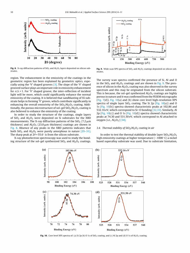
ig. 8. X-ray diffraction patterns of SiO2 and Al2O3 layers deposited on silicon sub-trates.
egion. The enhancement in the emissivity of the coatings in theeometric region has been explained by geometric optics, espe-ially using the ‘V’ shaped grooves [3]. The slope of the ‘V’ shapedrooved surface plays an important role in emissivity enhancementor �/� > 1. For ‘V’ shaped groove, the inter-reflection of incidentight will be more, which could significantly enhance the normalmissivity of the coating. It is believed that sandblasting of SS sub-trate helps in forming ‘V’ groves, which contribute significantly innhancing the overall emissivity of the SiO2/Al2O3 coating. Addi-ionally, the porous microstructure of sol–gel SiO2/Al2O3 coating islso believed to enhance the emissivity of the coating.
In order to study the structure of the coatings, single layersf SiO2 and Al2O3 were deposited on Si substrates for the XRDeasurements. The X-ray diffraction patterns of the SiO2 (7.2 �m
hickness) and Al2O3 (23.0 �m thickness) coatings are shown inig. 8. Absence of any peaks in the XRD patterns indicates that
oth SiO2 and Al2O3 were purely amorphous in nature [29–31].he sharp peak at 2� = 55.6◦ is from the silicon substrate.X-ray photoelectron spectroscopy was used to study the bond-ng structure of the sol–gel synthesized SiO2 and Al2O3 coatings.
807876747270
Inte
nsi
ty(a
rb. u
nit
s)
Bind ing Energy (e V)
74.30 eV
Al
2p
10810610410210098
Inte
nsi
ty (
arb
. u
nit
s)
Binding Energy (eV)
Si
2p
102.86 eV(a) (b
(c) (
Fig. 10. Core level XPS spectra of: (a) Si 2p (b) O 1s of SiO2
Fig. 9. Wide scan XPS spectra of SiO2 and Al2O3 coatings deposited on silicon sub-strates.
The survey scan spectra confirmed the presence of Si, Al and Oin the SiO2 and Al2O3 coatings and are shown in Fig. 9. The pres-ence of silicon in the Al2O3 coating was also observed in the surveyspectrum and this may be originated from the silicon substrate.This is because, the sol–gel synthesized Al2O3 coatings are highlyporous in nature and it was confirmed from the FESEM micrographs(Fig. 7(d)). Fig. 10(a) and (b) show core level high-resolution XPSspectra of single layer SiO2 coating. The Si 2p (Fig. 10(a)) and O1s (Fig. 10(b)) spectra showed characteristic peaks at 102.86 and532.16 eV, which correspond to Si O bonding [32,33]. Similarly, Al2p (Fig. 10(c)) and O 1s (Fig. 10(d)) spectra showed characteristicpeaks at 74.30 and 531.50 eV, which correspond to Al attached tooxygen (i.e., Al2O3) [34].
3.4. Thermal stability of SiO2/Al2O3 coating in air
In order to test the thermal stability of double layer SiO2/Al2O3high emissivity coatings at higher temperature (∼1000 ◦C) a nickelbased superalloy substrate was used. Due to substrate limitation,
540537534531528525
O 1
s
Binding Energy (eV )
Inte
nsi
ty (
arb
. u
nit
s)
531.50 eV
540537534531528525
O 1
s
Inte
nsi
ty (
arb
. u
nit
s)
Binding Energy (eV)
532.16 eV)
d)
coating, and (c) Al 2p and (d) O 1s of Al2O3 coating.

Surfa
wSεhhedwdfiioehtwom(NXmc
tilA∼tabo
efocsa
4
bttsbvipacXcA
[[
[[
[
[
[
[[[
[[
[[[[[[
[
[[
[
[
[
[
D.B. Mahadik et al. / Applied
e have not measured thermal stability above 1000 ◦C. ThisiO2/Al2O3 coating deposited on superalloy substrate exhibited
= 0.94 and ̨ = 0.34 before heat treatment. This sample waseat-treated at 1000 ◦C in air atmosphere for 2 h in a resistiveeating furnace. After heat-treatment, the sample exhibited anmittance of 0.92 and an absorptance of 0.42. There is littleifference observed in the emissivity value after heat-treatment,hich may be attributed to the densification of the network andecomposition of carbohydrate groups [35]. Hence, this study con-rms that the SiO2/Al2O3 coatings are thermally stable at 1000 ◦C
n air atmosphere. As it has been discussed, the emissivity dependsn temperature, apart from other factors. It may be noted that themissivity values reported herein are measured at 82 ◦C. We firsteat-treated the sample at 1000 ◦C for 2 h and then cooled it downo room temperature. Subsequently, the emissivity measurementsere carried out. The heating of the sample led to crystallization
f the coating. The XRD pattern of the heated coating in thin filmode (glancing angle = 1◦) exhibited the presence of (1 1 1), (0 1 2),
1 0 4), (2 2 2) and (1 0 0) reflections of alumina (data not shown).o peaks corresponding to crystalline SiO2 were observed in theRD data as the thickness of Al2O3 layer was quite high and theeasurements were done in the thin film mode and hence X-rays
ould not have penetrated to the SiO2 layer.The high thermal stability of the SiO2/Al2O3 coating is attributed
o the fact that both SiO2 and Al2O3 are highly stable thermally. SiO2s formed by directional covalent bonds, and has a well-definedocal structure with a melting point of ∼1400 ◦C [36]. Similarly,l2O3 is formed by strong ionic bonds, having melting point of2072 ◦C [37]. As both the oxides exhibit high thermal stability,
he SiO2/Al2O3 double layer coating can be stable up to a temper-ture of ∼1300 ◦C. Also, due to the presence of strong bonding inoth oxides inter-diffusion or mixing of layers is not expected toccur at high temperature.
This work has scope for further improvement in enhancing themittance from 0.94 to ∼0.97 and decreasing the absorptance valuerom 0.33 to ∼0.2. This can be achieved by increasing the emittancef single layer SiO2 up to 0.90 by doping nanoceramic particles orarbon nanotubes in this layer [7]. The Al2O3 layer deposited onuch SiO2 coating can further enhance the emittance up to 0.97nd reduce the absorptance less than 0.20 [17].
. Conclusion
Double layer SiO2/Al2O3 coatings were deposited on sand-lasted SS substrate using spray deposition system at roomemperature. A simple and cost effective sol–gel method was usedo prepare SiO2 and Al2O3 sols. The optimized SiO2/Al2O3 coatinghows high emittance (0.94) and low absorptance (0.30) on sand-lasted SS substrate. The double layer SiO2/Al2O3 coating showedery low reflectance (<1%) in 2–20 �m wavelength region, whichs attributed to high emissivity of the coatings. The surface mor-hology of SiO2 coating deposited on Si substrate exhibited cracksnd Al2O3 coating deposited on Si substrate also exhibited signifi-
antly rough surface morphology with random cluster growth. TheRD data of the sol–gel prepared SiO2 and Al2O3 materials indi-ated their amorphous nature. The chemical bonding of SiO2 andl2O3 was further confirmed using XPS. SiO2/Al2O3 double layer[
[[
ce Science 299 (2014) 6–11 11
high emissivity coatings were thermally stable at 1000 ◦C in air withno appreciable change in the emittance and absorptance values.The double layer high emissivity SiO2/Al2O3 coatings are preparedusing a very simple and cost effective method with a freedom tocoat any size of the substrate. These coatings could be useful infurnace and spacecraft applications.
Acknowledgment
The authors thank the Director, CSIR-NAL for giving permissionto publish these results.
References
[1] K. Shimazaki, M. Imaizumi, K. Kibe, Thin Solid Films 516 (2008) 2218–2224.[2] M. Falz, G. Leonhardt, Surf. Coat. Technol. 61 (1993) 97–100.[3] X. He, Y. Li, L. Wang, Y. Sun, S. Zhang, Thin Solid Films 517 (2009)
5120–5129.[4] T. Olding, M. Sayer, D. Barrow, Thin Solid Films 398–399 (2001) 581–586.[5] R. Tucker, J. Ward, Appl. Energy 89 (2012) 127–132.[6] G.D. Stefanidis, K.M. Van Geem, G.J. Heynderickx, G.B. Marin, J. Chem. Eng. 137
(2008) 411–421.[7] J. Huang, Y. Li, X. He, G. Song, C. Fan, Y. Sun, W. Fei, S. Du, Appl. Surf. Sci. 259
(2012) 301–305.[8] X. Zhao, X.D. He, Y. Sun, L.D. Wang, Mater. Lett. 65 (2011) 2592–2594.[9] M. Benkahoul, M. Chaker, J. Margot, E. Haddad, R. Kruzelecky, B. Wong, W.
Jamroz, P. Poinas, Sol. Energy Mater. Sol. Cells 95 (2011) 3504–3508.10] J.E.J. Staggs, H.N. Phylaktou, Fire Saf. J. 43 (2008) 1–10.11] Cheng Xu-dong, Min Jie, Zhu Zhen-qi, Ye Wei-ping, Int. J. Miner. Metall. Mater.
19 (2012) 173–178.12] K. Shioya, Azabujuban Chome, Minato-ku, US Patent No. 4469721.13] Y.M. Wang, H. Tian, D.L. Quan, L.X. Guo, J.H. Ouyang, Y. Zhou, D.C. Jia, Surf. Coat.
Technol. 206 (2012) 3772–3776.14] H. Tang, T. Xin, Q. Sun, C. Yi, Z. Jiang, F. Wang, Appl. Surf. Sci. 257 (2011)
10839–10844.15] H. Tang, Q. Sun, T. Xin, C. Yi, Z. Jiang, F. Wang, Curr. Appl. Phys. 12 (2012)
284–290.16] A.K. Chelashaw, H. Wang, C. Wang, A.K. Kumi, L. Li, ARPN J. Eng. Appl. Sci. 7
(2012) 1228–1234.17] C.E. Holcombe Jr., L.R. Chapman, US Patent No. 5668072.18] G.J. Heynderickx, N. Masatsugu, Chem. Eng. Sci. 59 (2004) 5657–5662.19] C.J. Brinker, G.W. Scherer, Sol–Gel Science: The Physics and Chemistry of
Sol–Gel Processing, Academic Press, New York, 1990, pp. 98–108.20] M.A. Aegerter, N. Leventis, Aerogels Handbook, Springer, 2011.21] F. Ghmari, T. Ghbara, M. Laroche, R. Carminati, J.-J. Greffet, J. Appl. Phys. 96
(2004) 2556–2564.22] W. Li, D. Zhao, Adv. Mater. 25 (2013) 142–149.23] K. Tadanaga, N. Katata, T. Minami, J. Am. Ceram. Soc. 80 (1997) 3213–3216.24] J. Yi, X.D. He, Y. Sun, Y. Li, Appl. Surf. Sci. 253 (2007) 4361–4366.25] G. Feng, Y. Wang, Y. Li, J. Zhu, L. Zhao, Mater. Lett. 65 (2011) 1238–1240.26] H.W. Babel, H.G. Le, US Patent No. 5296235.27] A. Duffie, W.A. Beckman, Solar Engineering of Thermal Processes, 3rd ed., John
Wiley & Sons, Inc., 2006.28] G. Cao, S.J. Weber, S.O. Martin, M.H. Anderson, K. Sridharan, T.R. Allen, Nucl.
Eng. Des. 251 (2012) 78–83.29] H.R. Pouretedal, M. Kazemi, Int. J. Ind. Chem. 3 (20) (2012) 2–8.30] L.P. Singh, S.K. Bhattacharyya, G. Mishra, S. Ahalawat, Appl. Nanosci. 1 (2011)
117–122.31] S. Cava, S.M. Tebcherani, I.A. Souza, S.A. Pianaro, C.A. Paskocimas, E. Longo, J.A.
Varela, Mater. Chem. Phys. 103 (2007) 394–399.32] M. Andrulevicius, S. Tamulevicius, Y. Gnatyuk, N. Vityuk, N. Smirnova, A. Ere-
menko, Mater. Sci. 14 (2008) 8–14.33] D. Briggs, M.P. Seah, Practical Surface Analysis by Auger and X-ray Photoelec-
tron Spectroscopy, Wiley, New York, 1984.34] B. Vincent Christ, Handbook of Monochromatic Spectra, Wiley, 2000, pp.
43–66.35] D.B. Mahadik, A. Venkateswara Rao, A. Parvathy Rao, P.B. Wagh, S.V. Ingale, C.
Satish, Gupta, J. Colloid Interface Sci. 356 (2011) 298–302.36] J.A. Dalton, D.C. Presnall, J. Petrol. 39 (1998) 1953–1964.37] T.-S. Shih, I.-C. Chen, Mater. Trans. 46 (2005) 1868–1876.


