Embed Size (px)
Citation preview
1 | P a g e
Embedded Microcontrollers
LED Based Program Design
Author: Jordan Lee Mauro-Buhagiar
Student ID: P132135
Lecturer: Caerwyn Ash
2 | P a g e
Table of Contents Summary ................................................................................................................................................. 4
Chapter I - Introduction ....................................................................................................................... 5
1.1 Introduction to Microcontrollers ....................................................................................................... 5
Figure 1.10 – First ever microcontroller ................................................................................................. 5
Figure 1.12 – Different types of microcontrollers used in a range of devices .................................... 5
Chapter II - Literature Review ............................................................................................................ 7
2.1. Microcontroller - Design & Architecture ......................................................................................... 7
Figure 2.10 – Basic microcontroller structure & operation .................................................................... 7
2.2. Microcontroller and microprocessor Dissimilarities ........................................................................ 8
Figure 2.21 – Microprocessor and microcontroller disparity .................................................................. 8
2.3. Central Processing Unit (CPU) ........................................................................................................ 9
2.31. Memory .................................................................................................................................... 10
2.32. Input and Output (I/O) ......................................................................................................... 10
2.4. Microcontroller Organisation ......................................................................................................... 11
2.5. Microcontroller - Software program .............................................................................................. 12
2.6. Research of Program Development ............................................................................................... 13
2.61. Registers ................................................................................................................................... 13
Figure 2.610 – Map Register................................................................................................................. 13
Figure 2.611 – Binary values determine I/O ports ............................................................................ 14
Chapter III – Research Methodology ................................................................................................ 15
3.1. Design and Development of the circuit and software .................................................................... 15
Figure 3.11 – Circuit Block Diagram.................................................................................................... 15
Figure 3.12 – Program development block diagram......................................................................... 15
3.11 Circuit requirements ...................................................................................................................... 16
Figure 3.13 – Circuit diagram ............................................................................................................... 16
Figure 3.14 - Program test1 .............................................................................................................. 17
Figure 3.15 – LED flashing, on & off .............................................................................................. 18
3.2. Timer0 Module & Set-up ............................................................................................................... 19
Figure 3.21 - TMR0 Block Diagram ..................................................................................................... 19
3.3. Prescaler Set-up ............................................................................................................................. 20
Figure 3.31 – Option Register functionalities & Prescaler rate ............................................................ 20
Test 2 – Worked example 1 on time delays .......................................................................................... 21
Figure 3.32 – 1 Second time delay subroutine ...................................................................................... 21
Figure 3.33 – 1 second delay illustration .......................................................................................... 22
Test 3, worked example 2 on time delay (6seconds) ............................................................................ 23
Figure 3.34 – Time delay increased to 6 seconds ................................................................................. 23
3 | P a g e
Test 4 – Figure 3.35 – Four minute delay ............................................................................................. 23
Figure 3.36 – Circuit test when calling 4 minute delay ..................................................................... 24
Test 5 - Figure 3.37 – 1 hour delay ....................................................................................................... 24
Test 6 – Testing both delays together ................................................................................................... 24
Figure 3.38 – Program executing with an LED response ..................................................................... 25
Figure 3.39 – Rearranged program ................................................................................................... 25
Figure 3.310 - Test example .......................................................................................................... 26
Figure 3.311 – 6 Hour delay program with 4 minutes of ‘LED’ performance ..................................... 26
3.4 Print Circuit Board Design .............................................................................................................. 28
Figure 3.41 – Instructions towards a PCB design ................................................................................. 28
Figure 3.42 – Instructions to a circuit design .................................................................................... 29
Figure 3.43 – Full schematic design translated to PCB ................................................................. 30
Figure 3.45 – PCB design and instructions ........................................................................................ 31
Figure 3.46 – PCB Schematic Design ................................................................................................... 31
Figure 3.47 – PCB schematic & 3D view............................................................................................ 32
Figure 3.48 – PCB mounting solution ............................................................................................ 33
Figure 3.49 – Final design.................................................................................................................. 33
3.5 Design Demonstration .................................................................................................................... 34
Figure 3.51 – Circuit demonstration ..................................................................................................... 34
Figure 3.52 – Demonstration of program used ................................................................................ 35
Chapter IV – Cost of Materials ......................................................................................................... 36
4.1. Cost and Materials ......................................................................................................................... 36
Chapter V – Lateral Thinking ............................................................................................................... 37
5.1 Lateral Thinking – Other Possible Uses ......................................................................................... 37
Chapter VI - Conclusion .................................................................................................................... 38
6.1. Conclusion ..................................................................................................................................... 38
Chapter VII - Bibliography ................................................................................................................ 39
Bibliography ......................................................................................................................................... 39
Chapter VIII - Appendix .................................................................................................................... 41
Appendices ............................................................................................................................................ 41
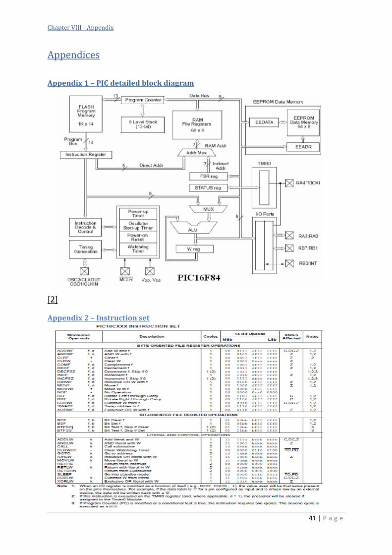
Appendix 1 – PIC detailed block diagram ............................................................................................ 41
Appendix 2 – Instruction set ............................................................................................................. 41
Appendix 3 – Complete Program .................................................................................................. 42
Appendix 4 – Program Flow Chart ....................................................................................................... 46

4 | P a g e
Summary The project relates to the design of a structured program composed in assembly language
that provides the feasibility of applying it to a variety of applications regarding an event. In
this case scenario, the program forces the microcontroller (PIC series) to trigger a light
emitting diode (LED - powered by a MOSFET transistor) every 6 hours for a timescale of 4
minutes. To complete a program as such, a prototype of a 24 hour digital clock was provided
to observe and analyse the program behind it. The 24 hour clock program became a great
assist to arrive at complete knowledge of the system’s working conditions, in relation to the
development of the project.
The report examines a step by step process designed to arrive at the completion of a
working program, providing extended abilities for the programmer to manipulate the
program with regards to their specifications.
Key points; Event – Program – Assembly Language – Trigger – LED – Every 6 hours – For 4
minutes
The step-by-step process consists of a direct approach that provides useful techniques on
how to set-up a simple program; distributing a learning curve that also includes timers and
delays. This allows the project to grow by stabilising the way of thinking. The report is
considered to deliver an advance level of knowledge to the reader regarding the PIC16F84
(or assembly language), explaining in complete detail how the device works, how the
processor links (to produce such performance) and how to program it using the exact
project requirements, as well as, a personal specification at different time scales, triggering
an event.
The objectives of the project and the desired performance were successfully achieved.
5 | P a g e
Chapter I - Introduction
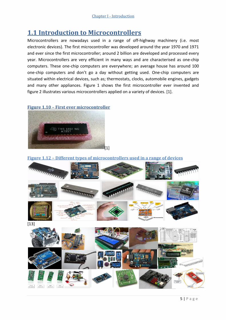
1.1 Introduction to Microcontrollers Microcontrollers are nowadays used in a range of off-highway machinery (i.e. most
electronic devices). The first microcontroller was developed around the year 1970 and 1971
and ever since the first microcontroller; around 2 billion are developed and processed every
year. Microcontrollers are very efficient in many ways and are characterised as one-chip
computers. These one-chip computers are everywhere; an average house has around 100
one-chip computers and don’t go a day without getting used. One-chip computers are
situated within electrical devices, such as; thermostats, clocks, automobile engines, gadgets
and many other appliances. Figure 1 shows the first microcontroller ever invented and
figure 2 illustrates various microcontrollers applied on a variety of devices. [1].
Figure 1.10 – First ever microcontroller
[1]
Figure 1.12 – Different types of microcontrollers used in a range of devices
[13]
6 | P a g e
[15](ii)
Project aim:
The aim of the project is to achieve a successful program that triggers an
event at specified times, with regards to the project brief. The program
will be demonstrated in a full schematic diagram of a circuit
implemented in Proteus. The circuit should be composed of a
microcontroller that controls an LED being powered by an NPN
transistor.
Project Objectives:
To develop a well-structured report regarding the complete design of
the project. The report must be divided into segments, segments that
dictate the development of the design and builds up to deliver
knowledge and understanding with regards to the systems performance
and production.
7 | P a g e
Chapter II - Literature Review
2.1. Microcontroller - Design & Architecture Microcontrollers [MCs] vary from a range of sources, and a plethora of designs. This project
is restricted to the microchip PIC series, 16F84 in particular.
Memory capacity varies widely from 0.5Kbytes to 512Kbytes of ‘Read Only Memory’ [ROM]
and 16bytes to 128Kbytes of ‘Random Access Memory’ [RAM] with 1Kbytes of flash
EEPROM. [2][3]
The PIC microchip series have become quite vast, microcontroller versions range from 8, 16
and 32 bits. Nowadays, microcontrollers are designed based on flash EEPROM; they can be
easily programmed and reprogrammed. [2][3]
The PIC 16F84 in particular consists of a Harvard Architecture design. MCs with Harvard
Architecture are called Reduced Instruction Set Computing (‘RISC’) microcontrollers. MCs
are designed in one of two architectures, Harvard or Von-Neumann [VN] known as Complex
Instruction Set Computing (‘CISC’) (I.e. Harvard = RISC, Von-Neumann = CISC) [2].
Harvard is an updated version of VN. Harvard allows a greater flow of data in and out of the
CPU at higher speed. This is caused by the Harvard design, having the data and address bus
separately connected. Additional information about microcontrollers will be discussed
further in the report. [2]
The main advantage of the ‘PIC16F84 MC’ is having a total of 35 instructions, all available
for execution in 1 instruction cycle except for the ‘JUMP’ and ‘BRANCH’ instructions. [2][3]
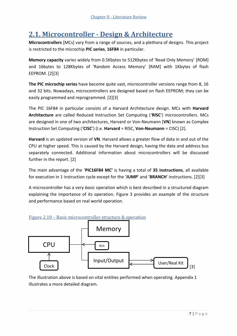
A microcontroller has a very basic operation which is best described in a structured diagram
explaining the importance of its operation. Figure 3 provides an example of the structure
and performance based on real world operation.
Figure 2.10 – Basic microcontroller structure & operation
[3]
The illustration above is based on vital entities performed when operating. Appendix 1
illustrates a more detailed diagram.
CPU
Input/Output
Memory
User/Real Kit
BUS
Clock
8 | P a g e
2.2. Microcontroller and microprocessor Dissimilarities Microcontrollers are typically embedded systems. An embedded system is composed of an
external processor, followed by an internal design regarding memory and I/O ports. As
both, the memory and I/O ports are integrated; the circuit is miniature, making a great
invention that is usually used in compact systems/devices, with the advantage of buying
them at low-cost. They are extremely beneficial as external components as they operate at
low voltages, keeping power consumption at a minimum. An extended functionality is also
available; power saving and idle mode, decreasing its power consumption even further.
Therefore, it has the ability to run with stored power (batteries), at an exquisite speed
performance, since all components and operations are integrated. The design also consists
of more registers than the microprocessor and therefore, makes the programming of the
software straightforward. The program memory in the microcontroller is designed with its
own memory location. [1][9]
Microprocessors are based on computer systems. The main difference between the two is
that a microprocessor is basically a processor and nothing else. Memory and I/O
components are adapted externally, therefore, forcing the design of the circuit to be bigger,
as well as, inefficient. Having all microprocessor components externally connected, requires
more power, making it impossible for stored power to create an efficient voltage-drive,
forcing the mains to power-up the circuit. Microprocessors are usually not found in compact
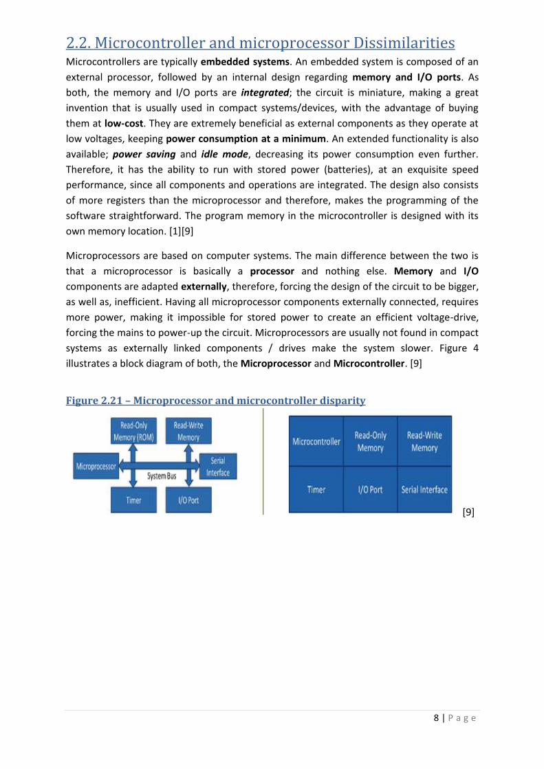
systems as externally linked components / drives make the system slower. Figure 4
illustrates a block diagram of both, the Microprocessor and Microcontroller. [9]
Figure 2.21 – Microprocessor and microcontroller disparity
[9]
9 | P a g e
2.3. Central Processing Unit (CPU)
CPU focuses on most calculations performed during execution, as well as, present
operations of all other units. CPU is best described as a synchronous device where all the
statistics are intercepted in parallel format, processing at a speed directly proportioned to
the clock. CPU’s are designed to follow some form of operation. The operation designed for
most CPU’s to follow involves four steps (fetch, decode, execute and write-back). [4]
Fetch – Reading an instruction represented in computer language (binary/hexadecimal)
from a memory location indicated by the software program. Memory locations are mapped
in the program counter. The program counter stores a value that determines its current
position within the program for the CPU to read. The length of the instruction determines
the size of memory that is required and therefore the program counter is incremented by
the required size. [4]
Decode –The instruction obtained is broken down into separate entities and is divided to
different portions of the CPU. Each division is significant to different parts of the CPU where
each stat is acknowledged by the CPU’s ‘Instruction Set Architecture’. Operands are known
to be the remaining portions of the instruction. Remaining portions are normally values,
which defines the action required for additional operation. [4]
Execution – At this point the CPU has read the instruction and now understands its
requirements. Therefore, different portions of the CPU work together performing the
desired operation. [4]
Execution refers to a sequence of stored instructions known as the program. This program
signifies a series of data (usually represented in binary / hexadecimal figures) and are then
stored in a non-volatile fashion within a memory location. [4]
If any other operations are requested, such as; input logics or arithmetic. The ‘Arithmetic
Logic Unit’ is then activated to a set of I/O ports (input/output) and takes care of it. [3]
Write-back – Defines the write back of any results to the required memory location
(ROM/RAM). [4]
Arithmetic and Logic Unit – This particular register focuses in all arithmetic and logic
operations where it utilises a source known as the regulator to keep a referenced voltage
and an accumulator used for logic operations.
10 | P a g e
2.31. Memory Computer memory stores memory in slots (memory locations). The program stored should
remain unchanged for good performance. Therefore, any data that requires the CPU to read
and follow should be stored in the ‘Read Only Memory’ (ROM – memory remains stored,
even when powered off and cannot be easily altered).
There are two types of memory, ROM as explained above and RAM. RAM is a term used for
‘Random Access Memory’. RAM is also read by the CPU, however, the CPU understands
that memory being stored in this type of location, may require a change of variables without
distracting any other location (RAM – Memory can be accessed randomly at any point in
time from any physical location allowing quick access and manipulation). [3]
2.32. Input and Output (I/O) Without this operation the microcontroller might be useless. Input and output is vital as it
allows the microprocessor to connect to the outside world. Allowing data transfer from the
microcontroller to external devices and peripherals. Data transfer may contain one of the
following:
- Status
- Control signals
- Data
Input and output’s - General purpose for performance:
1. Reconsider time difference between the microprocessor and peripherals.
2. Making sure data is formatted correctly.
3. It should handle the ‘status’ and the ‘control of signals’.
4. Must supply the correct voltage and current levels
5. [3]
Input stage makes sure that information is processed into systems. Such as, information
read from sensors or switches. It is defined as ‘Read Variable Operation’. [5]
Output stage is involved in processing information to the outside world and displaying the
results, normally used to control equipment. This is defined as ‘Write Variable Operation’.
[5]
11 | P a g e
2.4. Microcontroller Organisation The best way to consider the organisation of microcontrollers is to refer memory and I/O as
a series of discrete memory locations. Each of them encoded with its unique location
individually stored in binary words. Each word is considered to have 1 byte of data available.
Memory and I/O locations may be referred to as 8 times D-type flip flops connected in
parallel and is characterised as an 8-bit storage register. [3]
Buses are known to be crucial in any computer system. Microcontrollers normally involve
three buses performing different tasks.
- Address Bus
- Data Bus
- Control Bus
Buses are designed to transmit words of command information via sets of wires connected
in parallel. [3].
The address bus is for the CPU to transmit memory addresses back and forth. Allowing
transportation of data to be retrieved or deposited from correct locations. In other words, a
system used to address the main system memory. The address bus can vary from 16, 20 and
32 bits large. [3][6]
The data bus transports data in a bi-directional form, ranging from the CPU, memory and
I/O ports built in 8 or 16 bits wide in size. In other words, it allows data transmission from
one component to another on a mother board, system board or computer systems. [3][7]
The control bus on the other hand, decides which bus is required for data transmission. The
CPU utilises it to communicate with other entities inside the machine and a series of status
bits indicate the type of bus access required to take action. Signals that relate to read, write
and interrupt, allows the CPU to “visualize” and monitor the different parameters within a
computer system. Its exact composition varies amongst processors. [3][8]
12 | P a g e
2.5. Microcontroller - Software program Microcontrollers can be programmed using a variety of programming languages, such as C,
Assembly or BASIC, for instance. However, the language that contributes with the finest
performance is known to be the assembly language. Assembly language has excellent
reviews and is mostly preferred regarding engineers. It works amazingly well when
programming inexpensive MCs, as it drives them to the best of their abilities. This type of
language has one thing that no other program encounters; that is complete control of all
instructions followed by the CPU, along with memory and time control throughout each
instruction of the program. An assembly program is composed by reviewing the main
concept that needs to be achieved in extreme detail, following the steps that a computer
requires to ‘understand’. In other words, the complexity of the assembler has to be reduced
by writing in well defined format. Every CPU uses a different type of assembly language;
Pentiums, PIC microcontrollers, Microprocessors and Motorola 68000’s, making it harder to
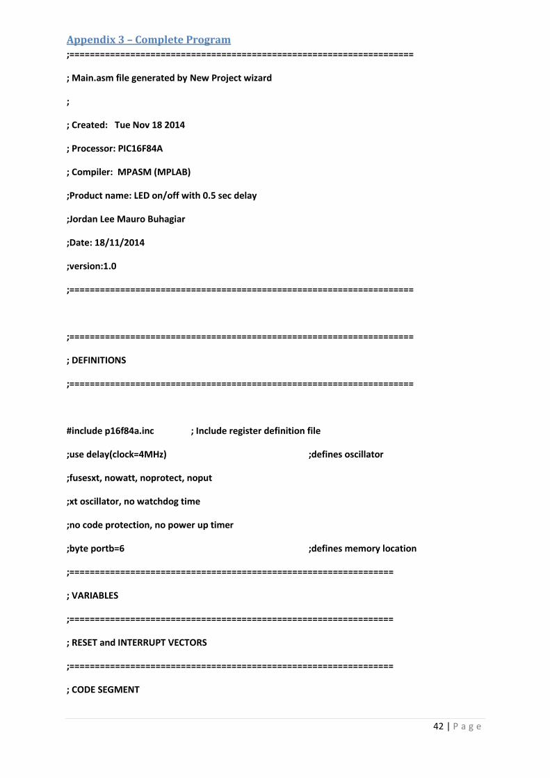
read/write, learn and understand. [9] Appendix 2 illustrates the PIC’s instruction set.
PIC16f84 is a high-tech microcontroller which is characterised as a micro-computer. Both,
the microcontroller and the microprocessor are much alike, having a sort of linkage with the
following:
Central processing unit (CPU)
Program memory (PROM)
Working memory (RAM)
Input / output (I/O)
Program counter
Registers – Special Function (SFR) & General Purpose (GPR)
Arithmetic Logic Unit (ALU)
Timers
Etc
Although a computer is designed in a higher level of complexity, the microcontroller is an
amazing design. The CPU is usually defined as the brain’s of a computer where most
calculations take place, sometimes referred as central processor or the heart of a computer.
As discussed earlier, the ‘16f84’ has a desirable advantage which consists of flash EEPROM.
In other words, flash EEPROM is considered to be a standard design which allows you to
erase or record data electrically, as well as, preserve any load of data when powered off. [3]
13 | P a g e
2.6. Research of Program Development Programming this type of project in assembler requires knowledge on the software process
operations, such as:
- Registers
- Banks
- Program execution
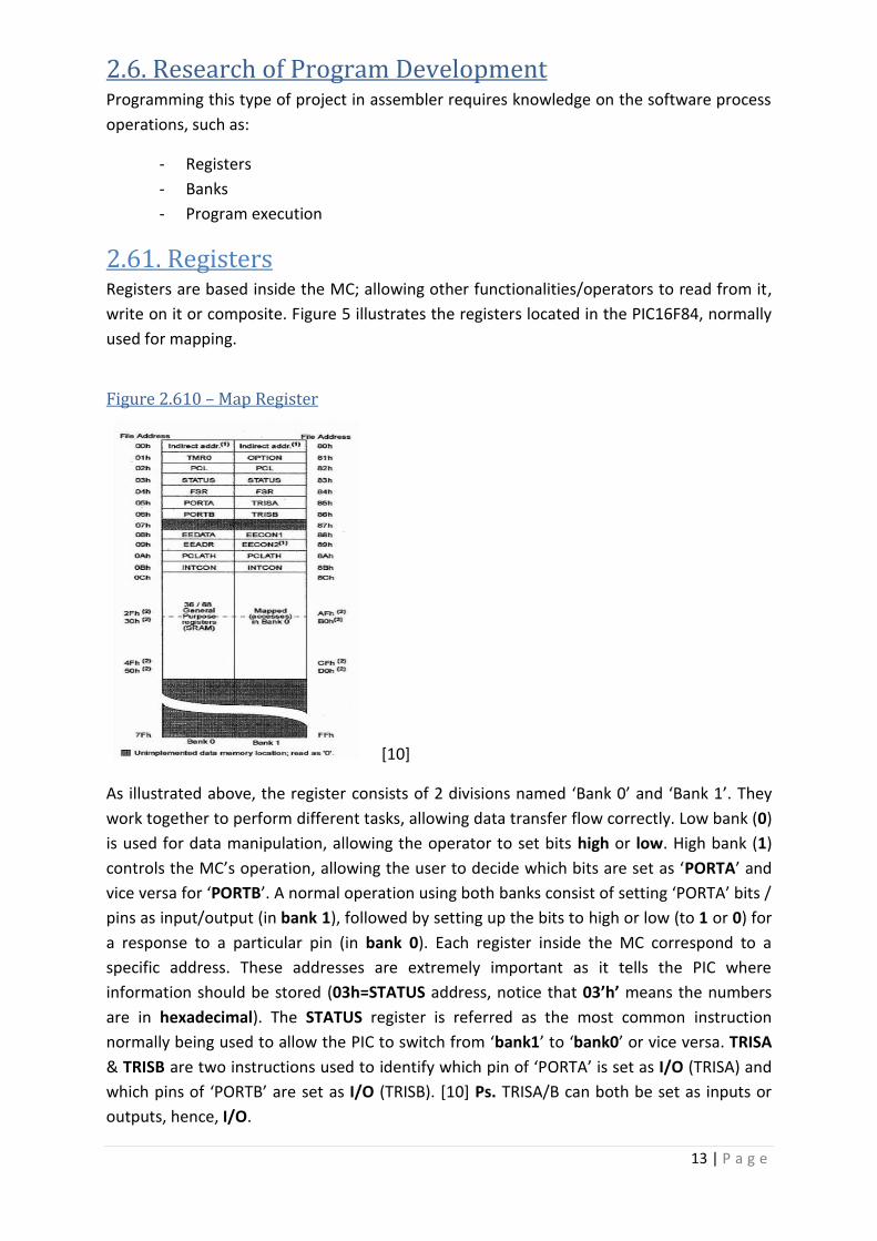
2.61. Registers Registers are based inside the MC; allowing other functionalities/operators to read from it,
write on it or composite. Figure 5 illustrates the registers located in the PIC16F84, normally
used for mapping.
Figure 2.610 – Map Register
[10]
As illustrated above, the register consists of 2 divisions named ‘Bank 0’ and ‘Bank 1’. They
work together to perform different tasks, allowing data transfer flow correctly. Low bank (0)
is used for data manipulation, allowing the operator to set bits high or low. High bank (1)
controls the MC’s operation, allowing the user to decide which bits are set as ‘PORTA’ and
vice versa for ‘PORTB’. A normal operation using both banks consist of setting ‘PORTA’ bits /
pins as input/output (in bank 1), followed by setting up the bits to high or low (to 1 or 0) for
a response to a particular pin (in bank 0). Each register inside the MC correspond to a
specific address. These addresses are extremely important as it tells the PIC where
information should be stored (03h=STATUS address, notice that 03’h’ means the numbers
are in hexadecimal). The STATUS register is referred as the most common instruction
normally being used to allow the PIC to switch from ‘bank1’ to ‘bank0’ or vice versa. TRISA
& TRISB are two instructions used to identify which pin of ‘PORTA’ is set as I/O (TRISA) and
which pins of ‘PORTB’ are set as I/O (TRISB). [10] Ps. TRISA/B can both be set as inputs or
outputs, hence, I/O.
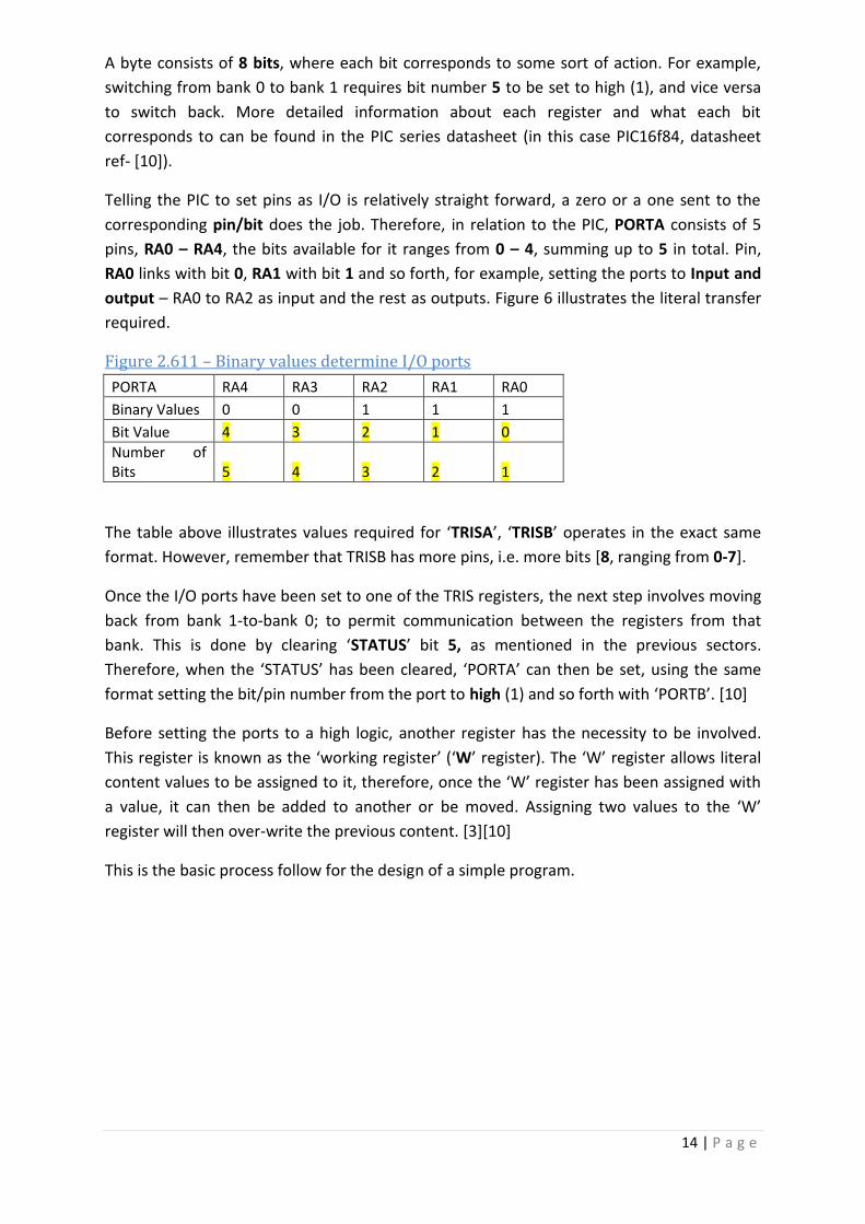
14 | P a g e
A byte consists of 8 bits, where each bit corresponds to some sort of action. For example,
switching from bank 0 to bank 1 requires bit number 5 to be set to high (1), and vice versa
to switch back. More detailed information about each register and what each bit
corresponds to can be found in the PIC series datasheet (in this case PIC16f84, datasheet
ref- [10]).
Telling the PIC to set pins as I/O is relatively straight forward, a zero or a one sent to the
corresponding pin/bit does the job. Therefore, in relation to the PIC, PORTA consists of 5
pins, RA0 – RA4, the bits available for it ranges from 0 – 4, summing up to 5 in total. Pin,
RA0 links with bit 0, RA1 with bit 1 and so forth, for example, setting the ports to Input and
output – RA0 to RA2 as input and the rest as outputs. Figure 6 illustrates the literal transfer
required.
Figure 2.611 – Binary values determine I/O ports
PORTA RA4 RA3 RA2 RA1 RA0
Binary Values 0 0 1 1 1
Bit Value 4 3 2 1 0
Number of Bits 5 4 3 2 1
The table above illustrates values required for ‘TRISA’, ‘TRISB’ operates in the exact same
format. However, remember that TRISB has more pins, i.e. more bits [8, ranging from 0-7].
Once the I/O ports have been set to one of the TRIS registers, the next step involves moving
back from bank 1-to-bank 0; to permit communication between the registers from that
bank. This is done by clearing ‘STATUS’ bit 5, as mentioned in the previous sectors.
Therefore, when the ‘STATUS’ has been cleared, ‘PORTA’ can then be set, using the same
format setting the bit/pin number from the port to high (1) and so forth with ‘PORTB’. [10]
Before setting the ports to a high logic, another register has the necessity to be involved.
This register is known as the ‘working register’ (‘W’ register). The ‘W’ register allows literal
content values to be assigned to it, therefore, once the ‘W’ register has been assigned with
a value, it can then be added to another or be moved. Assigning two values to the ‘W’
register will then over-write the previous content. [3][10]
This is the basic process follow for the design of a simple program.
15 | P a g e
Chapter III – Research Methodology
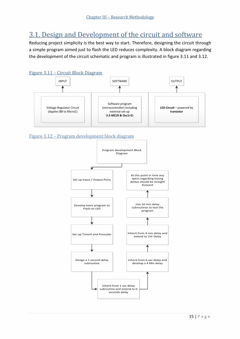
3.1. Design and Development of the circuit and software Reducing project simplicity is the best way to start. Therefore, designing the circuit through
a simple program aimed just to flash the LED reduces complexity. A block diagram regarding
the development of the circuit schematic and program is illustrated in figure 3.11 and 3.12.
Figure 3.11 – Circuit Block Diagram
LED Circuit – powered by transistor
Voltage Regulator Circuit(Applies 5V to MicroC)
Software program (microcontroller) including
external set-up (I.E-MCLR & Osc1+2)
INPUT SOFTWAREINPUT OUTPUT
Figure 3.12 – Program development block diagram
Develop basic program to Flash an LED
Set-up Timer0 and Prescaler
Design a 1 second delay subroutine
Set-up Input / Output Ports
Inherit from 1 sec delay subroutine and extend to 6
seconds delay
Inherit from 6 sec delay and develop a 4 Min delay
Inherit from 4 min delay and extend to 1Hr Delay
Use 10 min delay subroutines to test the
program
At this point in time any specs regarding timing
delays should be straight forward
Program development Block Diagram
16 | P a g e
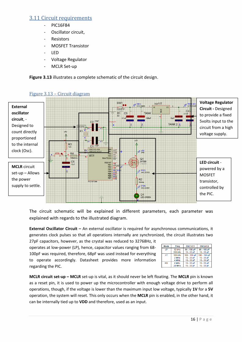
3.11 Circuit requirements - PIC16F84
- Oscillator circuit,
- Resistors
- MOSFET Transistor
- LED
- Voltage Regulator
- MCLR Set-up
Figure 3.13 illustrates a complete schematic of the circuit design.
Figure 3.13 – Circuit diagram
The circuit schematic will be explained in different parameters, each parameter was
explained with regards to the illustrated diagram.
External Oscillator Circuit – An external oscillator is required for asynchronous communications, it
generates clock pulses so that all operations internally are synchronized, the circuit illustrates two
27pF capacitors, however, as the crystal was reduced to 32768Hz, it
operates at low-power (LP), hence, capacitor values ranging from 68-
100pF was required, therefore, 68pF was used instead for everything
to operate accordingly. Datasheet provides more information
regarding the PIC.
MCLR circuit set-up – MCLR set-up is vital, as it should never be left floating. The MCLR pin is known
as a reset pin, it is used to power up the microcontroller with enough voltage drive to perform all
operations, though, if the voltage is lower than the maximum input low voltage, typically 1V for a 5V
operation, the system will reset. This only occurs when the MCLR pin is enabled, in the other hand, it
can be internally tied up to VDD and therefore, used as an input.
External
oscillator
circuit, -
Designed to
count directly
proportioned
to the internal
clock (Osc).
LED circuit -
powered by a
MOSFET
transistor,
controlled by
the PIC.
Voltage Regulator
Circuit - Designed
to provide a fixed
5volts input to the
circuit from a high
voltage supply.
MCLR circuit
set-up – Allows
the power
supply to settle.
17 | P a g e
In this project, MCLR pin has been configured with RESET functionality, with a push button/ switch
to manually reset the system’s operation.
Voltage Regulator – Voltage regulator is an extremely useful source for protection regarding the
circuit. For instance, the circuit requires 5 volts in to power up the microcontroller and from 2 - 3
volts approximately to power up the LED, thus, if you plug a 10 Volts supply, the circuit /
components will be jeopardised. Therefore, the voltage regulator acts like a safety net that no
matter how much voltage is being supplied, the voltage will be reduced to 5 volts. (19)
LED Circuit – The LED is being powered by a transistor (MOSFET, N-Channel), as specified in the
project brief, however, a MOSFET / normal NPN transistor can be applied, though; a MOSFET has
been selected instead. Reason being, the MOSFET is voltage based and the NPN is current based.
This means that a MOSFET does not require a resistor between the PIC and the transistor, as
voltage is usually stable, current, in the other hand, may require some control
(resistor) to avoid the current spikes. The gate-source breakdown voltage is 2.5
volts approximately; hence, no further calculations are required to power-up the
LED, (as long as 2-3 volts is being supplied to it). Figure 3.13 proves 2.2 volts
approximately is being supplied. (16)
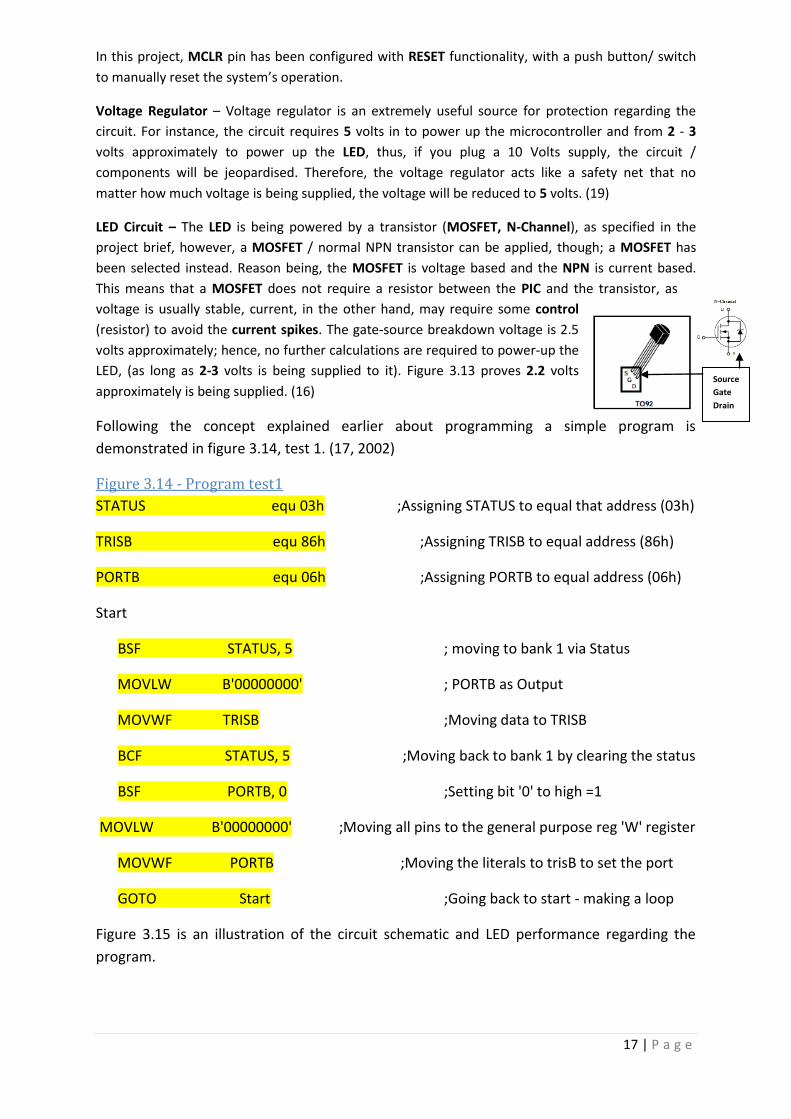
Following the concept explained earlier about programming a simple program is
demonstrated in figure 3.14, test 1. (17, 2002)
Figure 3.14 - Program test1
STATUS equ 03h ;Assigning STATUS to equal that address (03h)
TRISB equ 86h ;Assigning TRISB to equal address (86h)
PORTB equ 06h ;Assigning PORTB to equal address (06h)
Start
BSF STATUS, 5 ; moving to bank 1 via Status
MOVLW B'00000000' ; PORTB as Output
MOVWF TRISB ;Moving data to TRISB
BCF STATUS, 5 ;Moving back to bank 1 by clearing the status
BSF PORTB, 0 ;Setting bit '0' to high =1
MOVLW B'00000000' ;Moving all pins to the general purpose reg 'W' register
MOVWF PORTB ;Moving the literals to trisB to set the port
GOTO Start ;Going back to start - making a loop
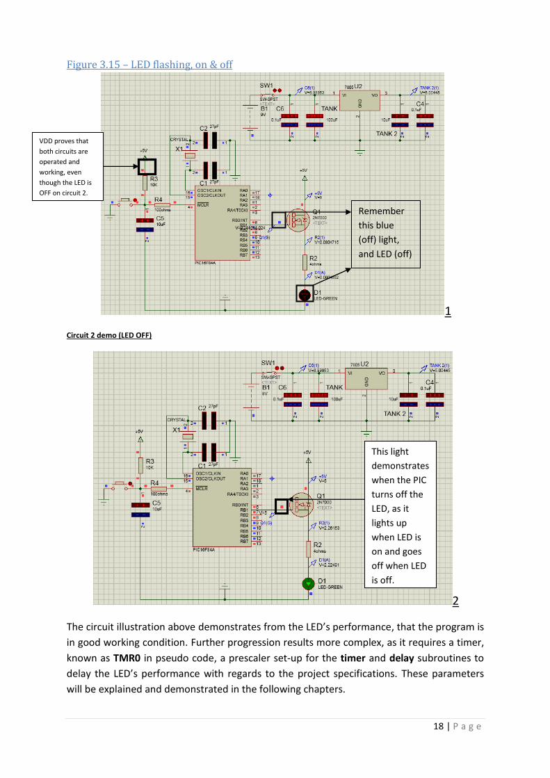
Figure 3.15 is an illustration of the circuit schematic and LED performance regarding the
program.
Source
Gate
Drain
18 | P a g e
Figure 3.15 – LED flashing, on & off
1
Circuit 2 demo (LED OFF)
2
The circuit illustration above demonstrates from the LED’s performance, that the program is
in good working condition. Further progression results more complex, as it requires a timer,
known as TMR0 in pseudo code, a prescaler set-up for the timer and delay subroutines to
delay the LED’s performance with regards to the project specifications. These parameters
will be explained and demonstrated in the following chapters.
VDD proves that
both circuits are
operated and
working, even
though the LED is
OFF on circuit 2.
This light
demonstrates
when the PIC
turns off the
LED, as it
lights up
when LED is
on and goes
off when LED
is off.
Remember
this blue
(off) light,
and LED (off)
19 | P a g e
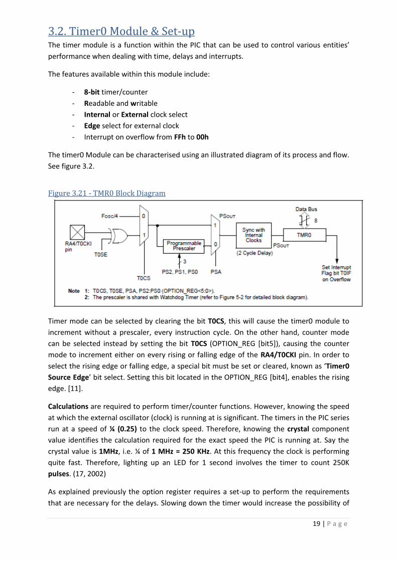
3.2. Timer0 Module & Set-up The timer module is a function within the PIC that can be used to control various entities’
performance when dealing with time, delays and interrupts.
The features available within this module include:
- 8-bit timer/counter
- Readable and writable
- Internal or External clock select
- Edge select for external clock
- Interrupt on overflow from FFh to 00h
The timer0 Module can be characterised using an illustrated diagram of its process and flow.
See figure 3.2.
Figure 3.21 - TMR0 Block Diagram
Timer mode can be selected by clearing the bit T0CS, this will cause the timer0 module to
increment without a prescaler, every instruction cycle. On the other hand, counter mode
can be selected instead by setting the bit T0CS (OPTION_REG [bit5]), causing the counter
mode to increment either on every rising or falling edge of the RA4/T0CKI pin. In order to
select the rising edge or falling edge, a special bit must be set or cleared, known as ‘Timer0
Source Edge’ bit select. Setting this bit located in the OPTION_REG [bit4], enables the rising
edge. [11].
Calculations are required to perform timer/counter functions. However, knowing the speed
at which the external oscillator (clock) is running at is significant. The timers in the PIC series
run at a speed of ¼ (0.25) to the clock speed. Therefore, knowing the crystal component
value identifies the calculation required for the exact speed the PIC is running at. Say the
crystal value is 1MHz, i.e. ¼ of 1 MHz = 250 KHz. At this frequency the clock is performing
quite fast. Therefore, lighting up an LED for 1 second involves the timer to count 250K
pulses. (17, 2002)
As explained previously the option register requires a set-up to perform the requirements
that are necessary for the delays. Slowing down the timer would increase the possibility of
20 | P a g e
regaining accurate time measurements by reducing the number of cycles the
microcontroller is required to count to make 1 second. A varied factor of 2, 4, 8, 16, 32, 64,
128, 256 are available within the prescaler. These factors are known as prescaler ratios and
are used to divide the number of cycles per second by each corresponding ratio. If 250K
cycles would be equivalent to 1 second; setting the prescaler to 256 will cause a calculation
of 250K/256= 976.5625 (equivalent to 1 second once it is set). [11]
Due to the clock being so high in frequency, it increases complexity regarding the maths.
Reducing the internal clock frequency to 32 KHz slows down the process making delays
easier to perform. By using 32,768 KHZ as the external oscillator value allows the maths to
be straightforward and exact (whole digit; no fraction). ¼ of 32768Hz = 8192Hz, frequency =
1/time. Therefore, 8192Hz results as 8192 pulses, counting 8192 pulses will result as 1
second. However, 8192 pulses still results as a lot to count. This is when the prescaler is
introduced. [11] (17, 2002)
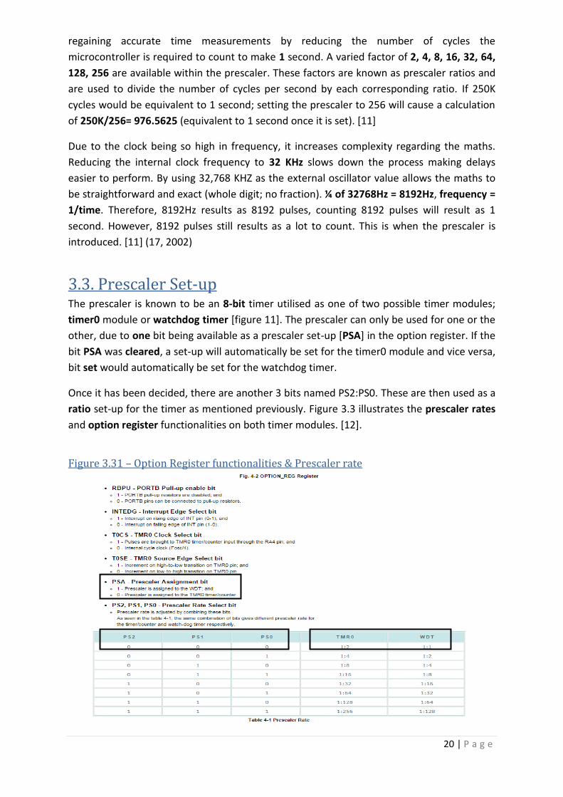
3.3. Prescaler Set-up The prescaler is known to be an 8-bit timer utilised as one of two possible timer modules;
timer0 module or watchdog timer [figure 11]. The prescaler can only be used for one or the
other, due to one bit being available as a prescaler set-up [PSA] in the option register. If the
bit PSA was cleared, a set-up will automatically be set for the timer0 module and vice versa,
bit set would automatically be set for the watchdog timer.
Once it has been decided, there are another 3 bits named PS2:PS0. These are then used as a
ratio set-up for the timer as mentioned previously. Figure 3.3 illustrates the prescaler rates
and option register functionalities on both timer modules. [12].
Figure 3.31 – Option Register functionalities & Prescaler rate
21 | P a g e
The illustration above demonstrates how to assign a definitive prescaler value for the WDT
& TMR0 module depending on the peripherals of the system. The prescaler values are
simply categorized into ratios to demonstrate the 3 bit binary format.
As illustrated on the figure above, it states how to choose different ratios by using diverse
binary values. [12].
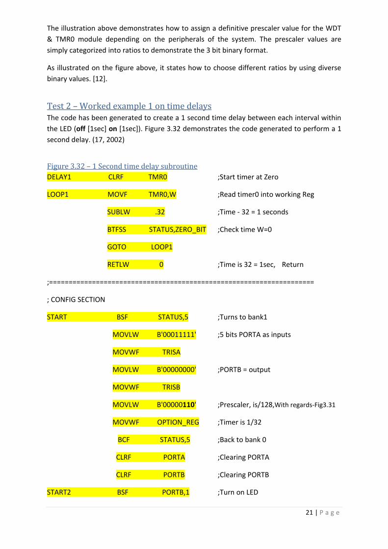
Test 2 – Worked example 1 on time delays The code has been generated to create a 1 second time delay between each interval within
the LED (off [1sec] on [1sec]). Figure 3.32 demonstrates the code generated to perform a 1
second delay. (17, 2002)
Figure 3.32 – 1 Second time delay subroutine
DELAY1 CLRF TMR0 ;Start timer at Zero
LOOP1 MOVF TMR0,W ;Read timer0 into working Reg
SUBLW .32 ;Time - 32 = 1 seconds
BTFSS STATUS,ZERO_BIT ;Check time W=0
GOTO LOOP1
RETLW 0 ;Time is 32 = 1sec, Return
;====================================================================
; CONFIG SECTION
START BSF STATUS,5 ;Turns to bank1
MOVLW B'00011111' ;5 bits PORTA as inputs
MOVWF TRISA
MOVLW B'00000000' ;PORTB = output
MOVWF TRISB
MOVLW B'00000110' ;Prescaler, is/128,With regards-Fig3.31
MOVWF OPTION_REG ;Timer is 1/32
BCF STATUS,5 ;Back to bank 0
CLRF PORTA ;Clearing PORTA
CLRF PORTB ;Clearing PORTB
START2 BSF PORTB,1 ;Turn on LED
22 | P a g e
CALL DELAY1 ;wait 1 second
BCF PORTB,1 ; Turn off LED
CALL DELAY1 ;wait 1 second
GOTO START2 ;Repeat from start2
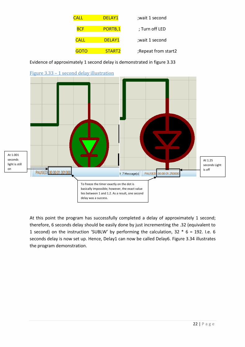
Evidence of approximately 1 second delay is demonstrated in figure 3.33
Figure 3.33 – 1 second delay illustration
At this point the program has successfully completed a delay of approximately 1 second;
therefore, 6 seconds delay should be easily done by just incrementing the .32 (equivalent to
1 second) on the instruction ‘SUBLW’ by performing the calculation, 32 * 6 = 192. I.e. 6
seconds delay is now set up. Hence, Delay1 can now be called Delay6. Figure 3.34 illustrates
the program demonstration.
At 1.001
seconds
light is still
on
At 1.25
seconds Light
is off
To freeze the timer exactly on the dot is
basically impossible; however, the exact value
lies between 1 and 1.2. As a result, one second
delay was a success.
23 | P a g e
Test 3, worked example 2 on time delay (6seconds)
Figure 3.34 – Time delay increased to 6 seconds
DELAY6 CLRF TMR0 ;Start timer at Zero
LOOP1 MOVF TMR0,W ;Read timer0 into working Reg
SUBLW .192 ;Time - 192 = 6 seconds (32*6)
BTFSS STATUS,ZERO_BIT ;Check time W=0
GOTO LOOP1 ;Time still not 0
RETLW 0 ;Time is now 0 = 192= 6sec, Return
The idea of 6 seconds delay is the process of making a 4 minutes delay as well as, a 1 hour
delay. By calling the 6 seconds delay 5 times will provide a 30 seconds delay, consequently,
by generating a counter of .8 will then cause a 4 minutes delay (as 30 seconds is equal to ½ a
minute, therefore, ½ *8 = 4). Meaning that by incrementing the count to a higher value will
allow a time delay of a larger time scale. An hour delay will result as a count of 120 (i.e. 120
* ½ = 60 minutes) calling this delay 6 times will add-up to the required 6 hour delay, a count
of 240 will also have an advantage of using a smaller program. However, a long ‘count’
process requires more compensation regarding time offsets. This is the reason why setting
up small delays provides more accurate results. Figure 3.35 demonstrates test 4 on a 4
minute delay subroutine set-up. (17, 2002)
Test 4 – Figure 3.35 – Four minute delay
FOUR_MINS_DELAY
MOVLW .8 ;Time .8 / ½ minute = 4mins
MOVWF COUNT ;put .8 into COUNT
LOOP2 CALL DELAY6 ;wait 6 seconds
CALL DELAY6 ;wait 6 seconds
CALL DELAY6 ;wait 6 seconds
CALL DELAY6 ;wait 6 seconds
CALL DELAY6 ;wait 6 seconds = 30 sec
DECFSZ COUNT ;decrementing by 1 from count
GOTO LOOP2 ;Still not Zero
RETLW 0 ;Time is now Zero = 4mins, time to execute
24 | P a g e
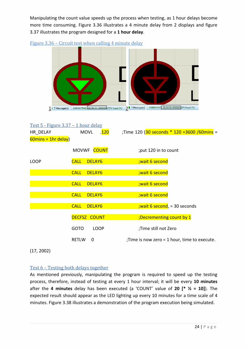
Manipulating the count value speeds up the process when testing, as 1 hour delays become
more time consuming. Figure 3.36 illustrates a 4 minute delay from 2 displays and figure
3.37 illustrates the program designed for a 1 hour delay.
Figure 3.36 – Circuit test when calling 4 minute delay
1 2
Test 5 - Figure 3.37 – 1 hour delay
HR_DELAY MOVL .120 ;Time 120 (30 seconds * 120 =3600 /60mins =
60mins = 1hr delay)
MOVWF COUNT ;put 120 in to count
LOOP CALL DELAY6 ;wait 6 second
CALL DELAY6 ;wait 6 second
CALL DELAY6 ;wait 6 second
CALL DELAY6 ;wait 6 second
CALL DELAY6 ;wait 6 second, = 30 seconds
DECFSZ COUNT ;Decrementing count by 1
GOTO LOOP ;Time still not Zero
RETLW 0 ;Time is now zero = 1 hour, time to execute.
(17, 2002)
Test 6 – Testing both delays together
As mentioned previously, manipulating the program is required to speed up the testing
process, therefore, instead of testing at every 1 hour interval; it will be every 10 minutes
after the 4 minutes delay has been executed (a ‘COUNT’ value of 20 [* ½ = 10]). The
expected result should appear as the LED lighting up every 10 minutes for a time scale of 4
minutes. Figure 3.38 illustrates a demonstration of the program execution being simulated.
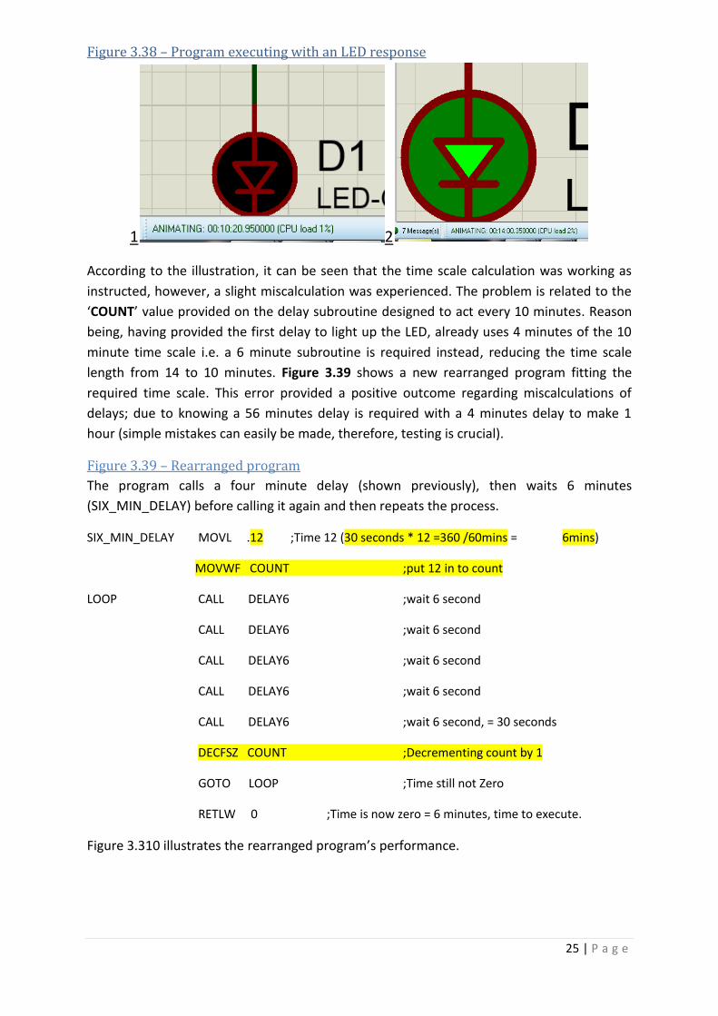
25 | P a g e
Figure 3.38 – Program executing with an LED response
1 2
According to the illustration, it can be seen that the time scale calculation was working as
instructed, however, a slight miscalculation was experienced. The problem is related to the
‘COUNT’ value provided on the delay subroutine designed to act every 10 minutes. Reason
being, having provided the first delay to light up the LED, already uses 4 minutes of the 10
minute time scale i.e. a 6 minute subroutine is required instead, reducing the time scale
length from 14 to 10 minutes. Figure 3.39 shows a new rearranged program fitting the
required time scale. This error provided a positive outcome regarding miscalculations of
delays; due to knowing a 56 minutes delay is required with a 4 minutes delay to make 1
hour (simple mistakes can easily be made, therefore, testing is crucial).
Figure 3.39 – Rearranged program
The program calls a four minute delay (shown previously), then waits 6 minutes
(SIX_MIN_DELAY) before calling it again and then repeats the process.
SIX_MIN_DELAY MOVL .12 ;Time 12 (30 seconds * 12 =360 /60mins = 6mins)
MOVWF COUNT ;put 12 in to count
LOOP CALL DELAY6 ;wait 6 second
CALL DELAY6 ;wait 6 second
CALL DELAY6 ;wait 6 second
CALL DELAY6 ;wait 6 second
CALL DELAY6 ;wait 6 second, = 30 seconds
DECFSZ COUNT ;Decrementing count by 1
GOTO LOOP ;Time still not Zero
RETLW 0 ;Time is now zero = 6 minutes, time to execute.
Figure 3.310 illustrates the rearranged program’s performance.
26 | P a g e
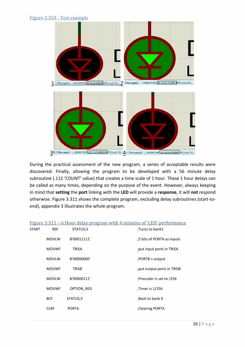
Figure 3.310 - Test example
1 2
3 4
During the practical assessment of the new program, a series of acceptable results were
discovered. Finally, allowing the program to be developed with a 56 minute delay
subroutine (.112 ‘COUNT’ value) that creates a time scale of 1 hour. These 1 hour delays can
be called as many times, depending on the purpose of the event. However, always keeping
in mind that setting the port linking with the LED will provide a response, it will not respond
otherwise. Figure 3.311 shows the complete program, excluding delay subroutines (start-to-
end), appendix 3 illustrates the whole program.
Figure 3.311 – 6 Hour delay program with 4 minutes of ‘LED’ performance START BSF STATUS,5 ;Turns to bank1
MOVLW B'00011111' ;5 bits of PORTA as inputs
MOVWF TRISA ;put input ports in TRISA
MOVLW B'00000000' ;PORTB = output
MOVWF TRISB ;put output ports in TRISB
MOVLW B'00000111' ;Prescaler is set to /256
MOVWF OPTION_REG ;Timer is 1/256
BCF STATUS,5 ;Back to bank 0
CLRF PORTA ;Clearing PORTA
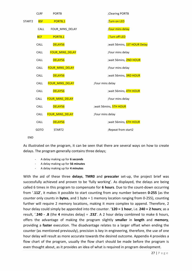
27 | P a g e
CLRF PORTB ;Clearing PORTB
START2 BSF PORTB,1 ;Turn on LED
CALL FOUR_MINS_DELAY ;Four mins delay
BCF PORTB,1 ; Turn off LED
CALL DELAY56 ;wait 56mins, 1ST HOUR Delay
CALL FOUR_MINS_DELAY ;Four mins delay
CALL DELAY56 ;wait 56mins, 2ND HOUR
CALL FOUR_MINS_DELAY ;Four mins delay
CALL DELAY56 ;wait 56mins, 3RD HOUR
CALL FOUR_MINS_DELAY ;Four mins delay
CALL DELAY56 ;wait 56mins, 4TH HOUR
CALL FOUR_MINS_DELAY ;Four mins delay
CALL DELAY56 ;wait 56mins, 5TH HOUR
CALL FOUR_MINS_DELAY ;Four mins delay
CALL DELAY56 ;wait 56mins, 6TH HOUR
GOTO START2 ;Repeat from start2
END
As illustrated on the program, it can be seen that there are several ways on how to create
delays. The program generally contains three delays;
- A delay making up for 6 seconds
- A delay making up for 56 minutes
- A delay making up for 4 minutes
With the aid of these three delays, TMR0 and prescaler set-up, the project brief was
successfully achieved and proven to be ‘fully working’. As displayed, the delays are being
called 6 times in this program to compensate for 6 hours. Due to the count-down occurring
from ‘.112’, it makes it possible to start counting from any number between 0-255 (as the
counter only counts in bytes, and 1 byte = 1 memory location ranging from 0-255), counting
further will require 2 memory locations, making it more complex to append. Therefore, 2
hour delay could simply be appended into the counter. ‘120 = 1 hour, i.e. 240 = 2 hours; as a
result, ‘.240 - .8 (the 4 minutes delay) = .232’. A 2 hour delay combined to make 6 hours,
offers the advantage of making the program slightly smaller in length and memory,
providing a faster execution. The disadvantage relates to a larger offset when ending the
counter (as mentioned previously), precision is key in engineering, therefore, the use of one
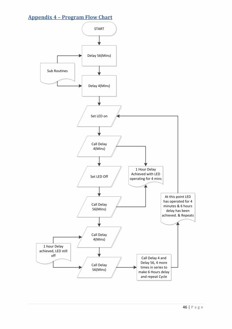
hour delay will result as more accurate towards the desired outcome. Appendix 4 provides a
flow chart of the program, usually the flow chart should be made before the program is
even thought about, as it provides an idea of what is required in program development.
28 | P a g e
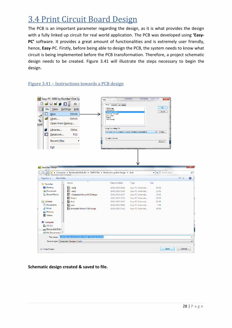
3.4 Print Circuit Board Design The PCB is an important parameter regarding the design, as it is what provides the design
with a fully linked up circuit for real world application. The PCB was developed using ‘Easy-
PC’ software. It provides a great amount of functionalities and is extremely user friendly,
hence, Easy-PC. Firstly, before being able to design the PCB, the system needs to know what
circuit is being implemented before the PCB transformation. Therefore, a project schematic
design needs to be created. Figure 3.41 will illustrate the steps necessary to begin the
design.
Figure 3.41 – Instructions towards a PCB design
Schematic design created & saved to file.
29 | P a g e
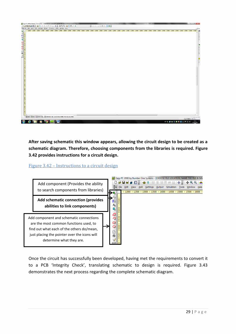
After saving schematic this window appears, allowing the circuit design to be created as a
schematic diagram. Therefore, choosing components from the libraries is required. Figure
3.42 provides instructions for a circuit design.
Figure 3.42 – Instructions to a circuit design
Once the circuit has successfully been developed, having met the requirements to convert it
to a PCB ‘Integrity Check’, translating schematic to design is required. Figure 3.43
demonstrates the next process regarding the complete schematic diagram.
Add component (Provides the ability
to search components from libraries)
Add schematic connection (provides
abilities to link components)
Add component and schematic connections
are the most common functions used, to
find out what each of the others do/mean,
just placing the pointer over the icons will
determine what they are.
30 | P a g e
Figure 3.43 – Full schematic design translated to PCB
Once the schematic has successfully been translated to a PCB design, building it up as
compact as possible is significant. Components can be selected and dragged to the PCB
schematic sheet from the component bin, having dragged all components, routing the
components is necessary with no overlaps regarding the nets (routes). If they do overlap,
there is a functionality that allows the nets to be placed at the bottom/top layer of the
board, solving many problems. Figure 3.44 illustrates the PCB design with relevant
instructions included to aid users.
Rainbow icon allows the
background sheet /
components colour to
be changed personally.
Integrity checks that the
circuit is linked
appropriately.
31 | P a g e
Figure 3.45 – PCB design and instructions
The following design in figure 3.46 will illustrate the final PCB with no sharp corners, a
copper layer (top and bottom) and fully labelled. The ( ) symbolises a demonstration of
the eliminated sharp corners, though it does not show all eliminated corners to provide a
good visual display of the schematic.
Figure 3.46 – PCB Schematic Design
Top Layer schematic with copper poured.
Side bar – provides; Layers,
Component bin, Add
component and Notes.
Shows all created files within
same project.
Left side icons follows the same concept as circuit schematic, placing pointer over
any icon provides a brief instruction regarding its operation. Icons in this side bar
are more sophisticated, also displaying copper pouring icon and more.
Design conclusion - The
idea of building a good PCB
revolves around; making it
compact and tidy, using a
design approach that
would reduce noise as
much as possible. I.e.
copper layers (bottom &
top), no sharp corners
cause it radiates.
32 | P a g e
Middle layer drill holes and zero nets.
Bottom Layer schematic with copper poured and direct routes from pin to pin present
(made to reduce complexity of overlapping routes).
Routes demonstrate the no sharp corners rule, to reduce noise interference as much as
possible. Figure 3.47 illustrates the design with all present layers in the same visual display,
followed by a high quality 3D view of the PCB final design.
Figure 3.47 – PCB schematic & 3D view
33 | P a g e
Last but not least, the board requires some sort of design to allow easy mounting, therefore,
arranging a way of employing it to an existing device is necessary. Figure 3.48 illustrates the
solution.
Figure 3.48 – PCB mounting solution
The solution as illustrated was solved by inserting drilling holes on each corner of the PCB
design for mounting purposes. A system design rule check was performed also, proving that
the PCB is in perfect condition with absolutely no errors. PCB is now ready for reproduction.
Figure 3.49 – Final design
Layer
thickness
can also be
reduced for
ease of
application
.
This was done
by deleting
unwanted layers
from –
Settings>Design
Technology>
Layers (Adv.
making a
compact mount)
Size: 35.2 x 36.5mm, Length: 143.41mm
34 | P a g e
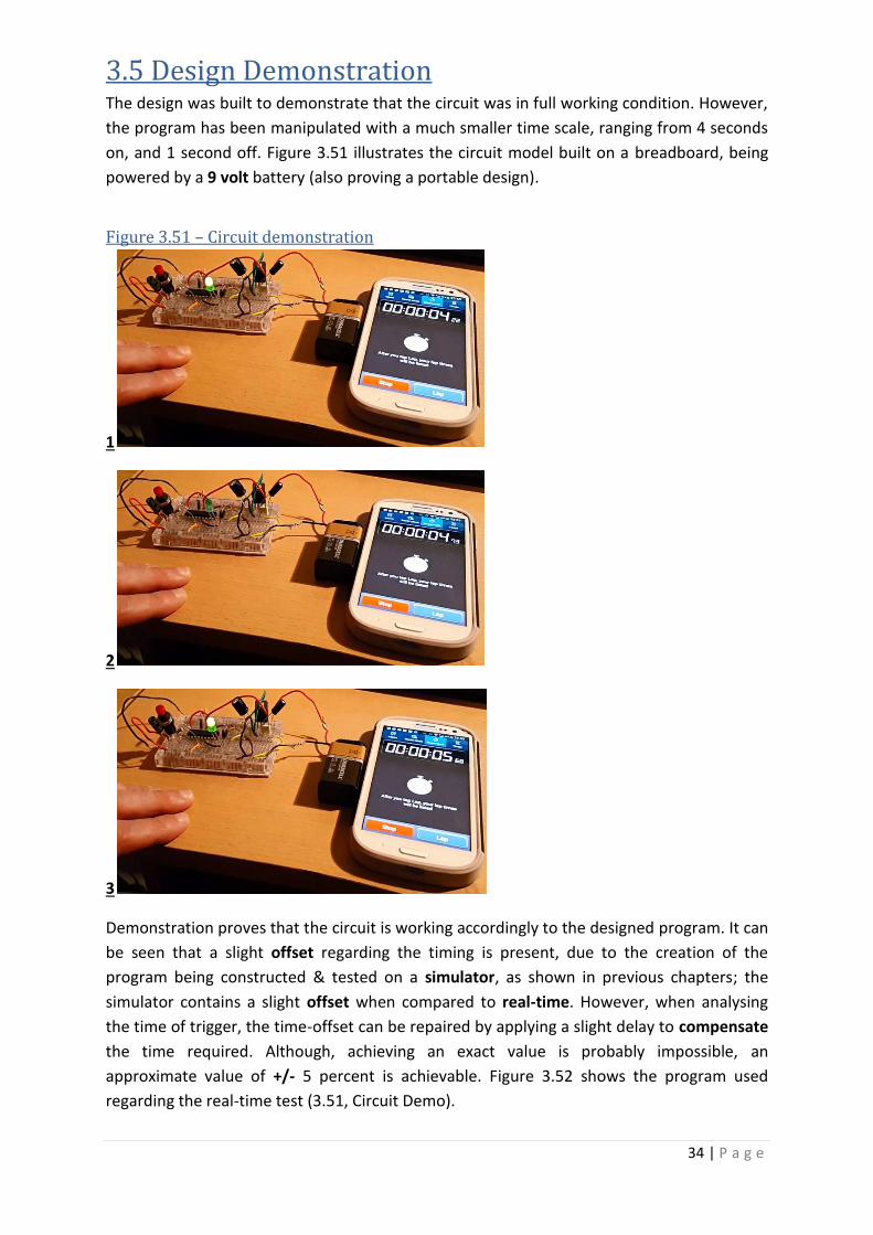
3.5 Design Demonstration The design was built to demonstrate that the circuit was in full working condition. However,
the program has been manipulated with a much smaller time scale, ranging from 4 seconds
on, and 1 second off. Figure 3.51 illustrates the circuit model built on a breadboard, being
powered by a 9 volt battery (also proving a portable design).
Figure 3.51 – Circuit demonstration
1
2
3
Demonstration proves that the circuit is working accordingly to the designed program. It can
be seen that a slight offset regarding the timing is present, due to the creation of the
program being constructed & tested on a simulator, as shown in previous chapters; the
simulator contains a slight offset when compared to real-time. However, when analysing
the time of trigger, the time-offset can be repaired by applying a slight delay to compensate
the time required. Although, achieving an exact value is probably impossible, an
approximate value of +/- 5 percent is achievable. Figure 3.52 shows the program used
regarding the real-time test (3.51, Circuit Demo).
35 | P a g e
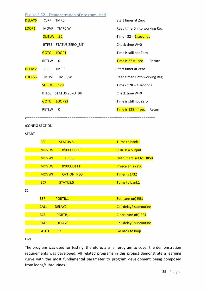
Figure 3.52 – Demonstration of program used
DELAY6 CLRF TMR0 ;Start timer at Zero
LOOP1 MOVF TMR0,W ;Read timer0 into working Reg
SUBLW .32 ;Time - 32 = 1 seconds
BTFSS STATUS,ZERO_BIT ;Check time W=0
GOTO LOOP1 ;Time is still not Zero
RETLW 0 ;Time is 32 = 1sec, Return
DELAY2 CLRF TMR0 ;Start timer at Zero
LOOP22 MOVF TMR0,W ;Read timer0 into working Reg
SUBLW .128 ;Time - 128 = 4 seconds
BTFSS STATUS,ZERO_BIT ;Check time W=0
GOTO LOOP22 ;Time is still not Zero
RETLW 0 ;Time is 128 = 4sec, Return
;====================================================================
;CONFIG SECTION
START
BSF STATUS,5 ;Turns to bank1
MOVLW B'00000000' ;PORTB = output
MOVWF TRISB ;Output are set to TRISB
MOVLW B'00000111' ;Prescaler is /256
MOVWF OPTION_REG ;Timer is 1/32
BCF STATUS,5 ;Turns to bank1
S2
BSF PORTB,1 ;Set (turn on) RB1
CALL DELAY2 ;Call delay2 subroutine
BCF PORTB,1 ;Clear (turn off) RB1
CALL DELAY6 ;Call delay6 subroutine
GOTO S2 ;Go back to loop
End
The program was used for testing; therefore, a small program to cover the demonstration
requirements was developed. All related programs in this project demonstrate a learning
curve with the most fundamental parameter to program development being composed
from loops/subroutines.
36 | P a g e
Chapter IV – Cost of Materials
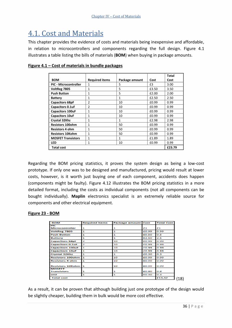
4.1. Cost and Materials This chapter provides the evidence of costs and materials being inexpensive and affordable,
in relation to microcontrollers and components regarding the full design. Figure 4.1
illustrates a table listing the bills of materials (BOM) when buying in package amounts.
Figure 4.1 – Cost of materials in bundle packages
BOM Required items Package amount Cost Total Cost
PIC - Microcontroller 1 5 £3 3.00
VoltReg 7805 1 5 £3.50 3.50
Push Button 1 5 £2.00 2.00
Battery 1 1 £2.50 2.50
Capacitors 68pF 2 10 £0.99 0.99
Capacitors 0.1uF 2 10 £0.99 0.99
Capacitors 100uF 1 10 £0.99 0.99
Capacitors 10uF 1 10 £0.99 0.99
Crystal 32Khz 1 1 £2.98 2.98
Resistors 100ohm 1 50 £0.99 0.99
Resistors 4 ohm 1 50 £0.99 0.99
Resistors 10Kohm 1 50 £0.99 0.99
MOSFET Transistors 1 1 £1.89 1.89
LED 1 10 £0.99 0.99
Total cost £23.79
Regarding the BOM pricing statistics, it proves the system design as being a low-cost
prototype. If only one was to be designed and manufactured, pricing would result at lower
costs, however, is it worth just buying one of each component, accidents does happen
(components might be faulty). Figure 4.12 illustrates the BOM pricing statistics in a more
detailed format, including the costs as individual components (not all components can be
bought individually). Maplin electronics specialist is an extremely reliable source for
components and other electrical equipment.
Figure 23 - BOM
(18)
As a result, it can be proven that although building just one prototype of the design would
be slightly cheaper, building them in bulk would be more cost effective.
37 | P a g e
Chapter V – Lateral Thinking
5.1 Lateral Thinking – Other Possible Uses The project may result as a very useful project with many possible uses. Nowadays, using
timers to perform executions or to trigger an event at different time intervals are of great
assistance for businesses / farms / etc. Jobs as such might be very easy to undertake,
therefore, why spend money on maintenance when a device can do a better job itself and
be consistent.
Programs are usually developed to complete or operate the easy jobs that for years were
performed by people themselves. A program is usually created to the level and specification
of user’s interest, and unlike people, the device will not require lunch break, fag break, toilet
break or anything else. It will perform the task using 100% of its ability every day or hour;
until the program is changed or updated to undertake other commitments, it is going to
operate as instructed. An example of a program being used at businesses may result from
locking a building automatically every day at the programmed times for security purposes.
These commitments can be fulfilled with no struggle and at low-cost, whereas, a person
would have to go around a building performing them and will await a pay cheque regularly.
This project for example can be used in many different fields and events, these events may
vary from the following;
- A locking system for a building
- Home / business security
- A green house
- Gardening (sprinklers)
- Temperature measures
- Alarms
- Street Lights
- And more
All these possible uses revolves around day-to-day routines/events, providing the solution
of affordable maintenance in a broad range of fields, making the project very useful
outdoors.

38 | P a g e
Chapter VI - Conclusion
6.1. Conclusion The project goal was an important field to study; gaining knowledge and understanding the
PIC series was relevant, to achieve a successful design. The ‘Assembly Language’ for
instance, became a self-teaching experience. However, it demonstrated that revising the
insides of the microchip in detail provided a very good understanding of how the
microcontroller acts when asked to commit or perform an endeavour. Therefore,
programming became slightly easier to learn.
Learning the ‘Assembly Language’ was significant as the language provides the facility of
working with a reduced number of instructions, yet, choosing an approach and actually
programming the microchip was extremely complex. After reviewing different articles and
books, programming became the strategy of an abbreviated ‘ladder’. A ladder, described in
a form of success, for each step closer to the top, meant a step closer to the finish.
Following specific steps of the report is guaranteed to teach a great deal of programming,
changing the way of thinking by providing the essential tools required to develop your own
circuit and program from a different specification at low-costs.
As results have shown; they proved that the project was successfully completed towards the
specified goal.
39 | P a g e
Chapter VII - Bibliography
Bibliography
[1] Electronic Circuits and Diagram-Electronics Projects and Design. (2013, October 23). Retrieved December
8, 2014, from http://www.circuitstoday.com/microcontroller-invention-history
[2] Al-Aubidy, P. (n.d.). Microcontroller Architecture. Retrieved December 4, 2014, from
http://www.philadelphia.edu.jo/academics/kaubaidy/uploads/ES-Slids-lec3.pdf
[3] Author: Caerwyn Ash – Course Notes
[4] Processor, M. (2009, September 10). Microprocesser. Retrieved December 6, 2014, from
http://microprocesser.blogspot.co.uk/2009/09/cpu-operation.html
[5] Input Process Output. (n.d.). Retrieved December 6, 2014, from
http://ict.stmargaretsacademy.org.uk/computing/hardware/ipo.html
[6] Inman, K., & Fritsky, L. (2014, December 1). What is an address bus. Retrieved December 6, 2014, from
http://www.wisegeek.com/what-is-an-address-bus.htm
[7] Husted, H. (2014, November 29). What Is a Data Bus? Retrieved December 7, 2014, from
http://www.wisegeek.org/what-is-a-data-bus.htm
[8] Lanz, C., & Wiley, M. (2014, December 3). What is a Control Bus? Retrieved December 7, 2014, from
http://www.wisegeek.com/what-is-a-control-bus.htm#didyouknowout
[9] Covington, M. (2004, January 1). PIC Assembly Language for the Complete Beginner. Retrieved December
9, 2014, from http://www.covingtoninnovations.com/noppp/picassem2004.pdf
[10] Microchip PIC16F84 Data Sheet. (2001, January 1). Retrieved December 9, 2014, from
http://ww1.microchip.com/downloads/en/DeviceDoc/35007b.pdf
[11] Book: PIC Microcontrollers. (n.d.). Retrieved December 9, 2014, from
http://www.mikroe.com/chapters/view/5/chapter-4-timers/)./
[12] PIC Instructions. (n.d.). Retrieved December 9, 2014, from http://tutor.al-williams.com/pic-inst.html
[14] Difference between Microprocessor and Microcontroller. (n.d.). Retrieved December 10, 2014, from
40 | P a g e
http://www.zseries.in/embedded lab/8051 microcontroller/difference between microprocessor and
microcontroller.php#.VK7fGCusVGl
[15] RAM & ROM. (n.d.). Retrieved January 29, 2015, from http://www.diffen.com/difference/RAM_vs_ROM
[16] Z. S. (n.d.). VN2222LL. Retrieved January 28, 2015, from Datasheet Catalog - datasheetcatalog.com :
http://pdf.datasheetcatalog.com/datasheet/zetexsemiconductors/vn2222ll.pdf
[17] D. W. (2002). PIC In Practice: A Project Approach. Oxford: Newnes.
[18] M. (n.d.). Maplin electrical components. Retrieved February 3, 2015, from The electronics specialist -
Maplin: http://www.maplin.co.uk/search?text=electrical+components&x=0&y=0
[19] L. D. (n.d.). Sparkfun - LM7805 Datasheet. Retrieved February 25, 2015, from Sparkfun:
https://www.sparkfun.com/datasheets/Components/LM7805.pdf
Images Ref:
Figure 1 –
[1] Electronic Circuits and Diagram (2013, October 23). Retrieved December 8, 2014, from
http://www.circuitstoday.com/microcontroller-invention-history
Figure 2 –
[13] Google images – Different microcontrollers in various applications
https://www.google.co.uk/search?q=microcontrollers&espv=2&biw=1242&bih=606&source
=lnms&tbm=isch&sa=X&ei=DKyAVLvMNJCR7AaN-IDwBQ&ved=0CAYQ_AUoAQ
Figure 2 (ii) –
[15] Google images – Devices using microcontrollers
https://www.google.co.uk/search?q=microcontrollers+used+in+a+variety+of+devices&espv
=2&biw=1366&bih=667&source=lnms&tbm=isch&sa=X&ei=V2jkVL__C8OC7gbwvICIBQ&ved
=0CAcQ_AUoAg#tbm=isch&q=devices+using+microcontrollers+&imgdii=_.
The rest of the images were obtained from articles and websites, carrying its own reference
from bibliography list.
#Kind regards
41 | P a g e
Chapter VIII - Appendix
Appendices
Appendix 1 – PIC detailed block diagram
[2]
Appendix 2 – Instruction set
42 | P a g e
Appendix 3 – Complete Program
;====================================================================
; Main.asm file generated by New Project wizard
;
; Created: Tue Nov 18 2014
; Processor: PIC16F84A
; Compiler: MPASM (MPLAB)
;Product name: LED on/off with 0.5 sec delay
;Jordan Lee Mauro Buhagiar
;Date: 18/11/2014
;version:1.0
;====================================================================
;====================================================================
; DEFINITIONS
;====================================================================
#include p16f84a.inc ; Include register definition file
;use delay(clock=4MHz) ;defines oscillator
;fusesxt, nowatt, noprotect, noput
;xt oscillator, no watchdog time
;no code protection, no power up timer
;byte portb=6 ;defines memory location
;================================================================
; VARIABLES
;================================================================
; RESET and INTERRUPT VECTORS
;================================================================
; CODE SEGMENT
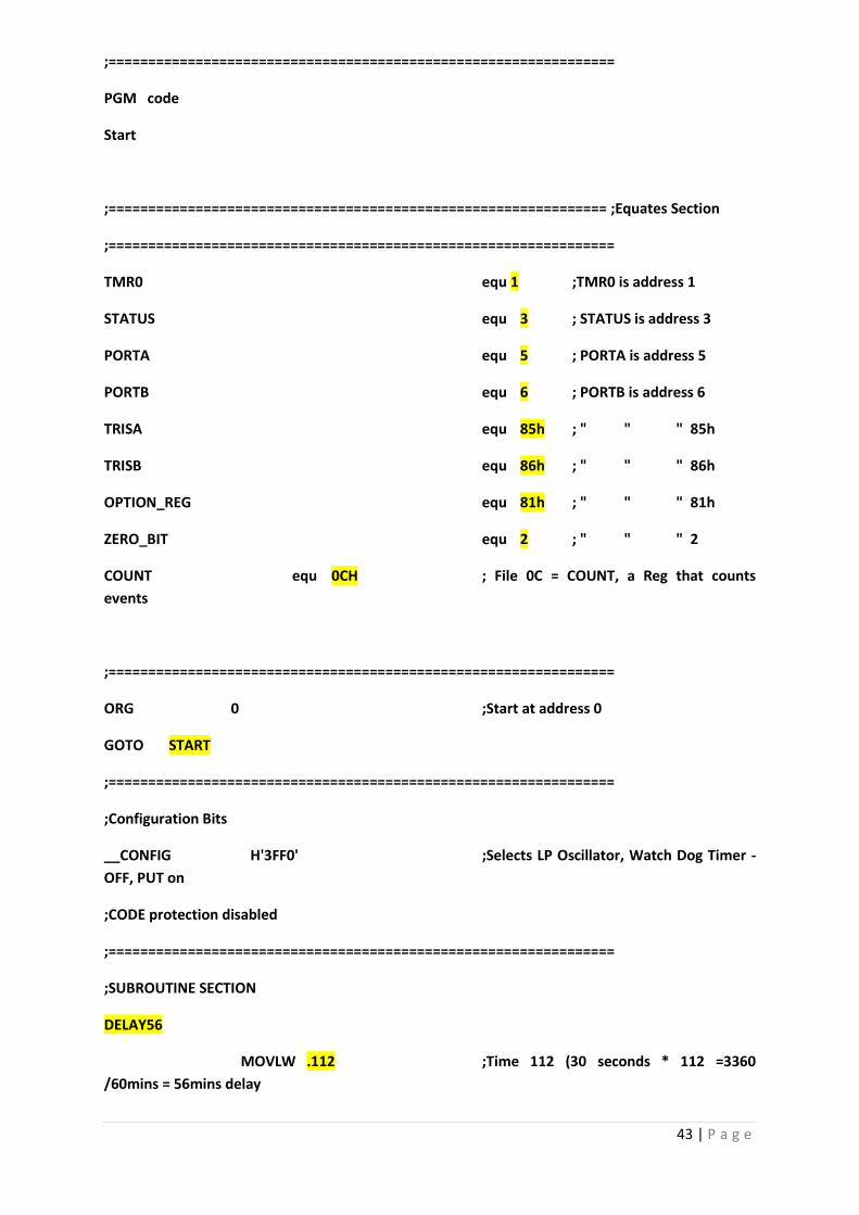
43 | P a g e
;================================================================
PGM code
Start
;=============================================================== ;Equates Section
;================================================================
TMR0 equ 1 ;TMR0 is address 1
STATUS equ 3 ; STATUS is address 3
PORTA equ 5 ; PORTA is address 5
PORTB equ 6 ; PORTB is address 6
TRISA equ 85h ; " " " 85h
TRISB equ 86h ; " " " 86h
OPTION_REG equ 81h ; " " " 81h
ZERO_BIT equ 2 ; " " " 2
COUNT equ 0CH ; File 0C = COUNT, a Reg that counts
events
;================================================================
ORG 0 ;Start at address 0
GOTO START
;================================================================
;Configuration Bits
__CONFIG H'3FF0' ;Selects LP Oscillator, Watch Dog Timer -
OFF, PUT on
;CODE protection disabled
;================================================================
;SUBROUTINE SECTION
DELAY56
MOVLW .112 ;Time 112 (30 seconds * 112 =3360
/60mins = 56mins delay
44 | P a g e
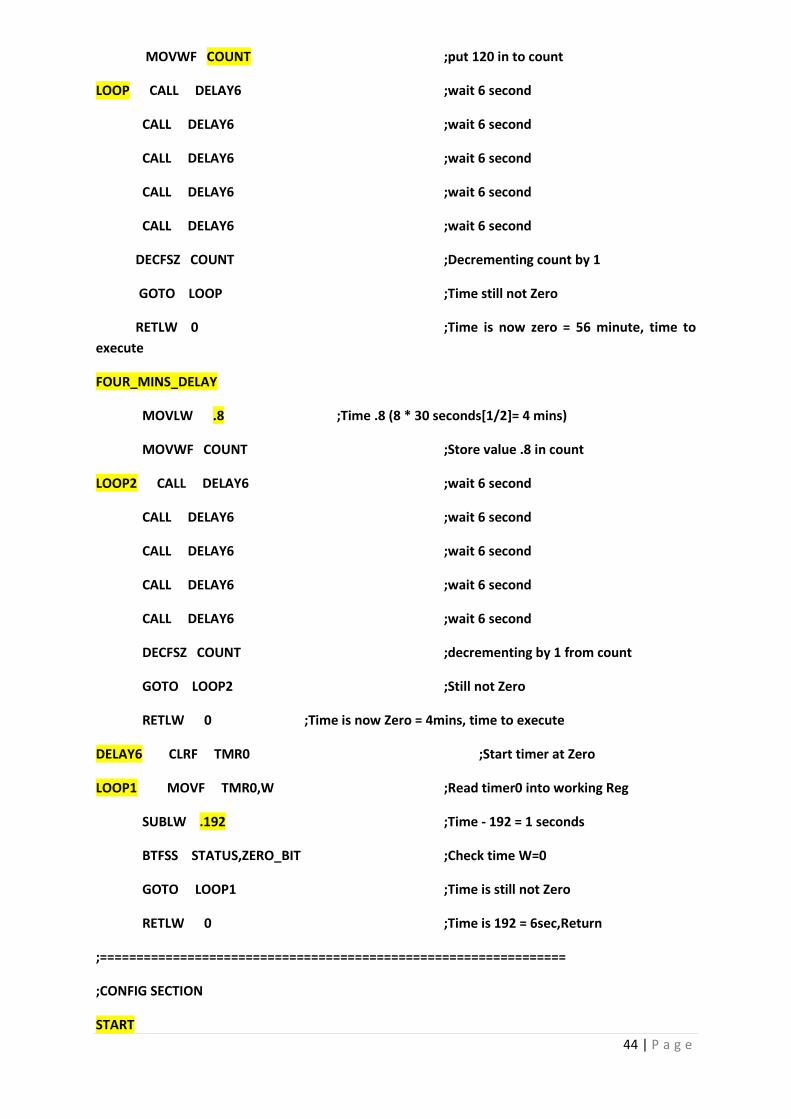
MOVWF COUNT ;put 120 in to count
LOOP CALL DELAY6 ;wait 6 second
CALL DELAY6 ;wait 6 second
CALL DELAY6 ;wait 6 second
CALL DELAY6 ;wait 6 second
CALL DELAY6 ;wait 6 second
DECFSZ COUNT ;Decrementing count by 1
GOTO LOOP ;Time still not Zero
RETLW 0 ;Time is now zero = 56 minute, time to
execute
FOUR_MINS_DELAY
MOVLW .8 ;Time .8 (8 * 30 seconds[1/2]= 4 mins)
MOVWF COUNT ;Store value .8 in count
LOOP2 CALL DELAY6 ;wait 6 second
CALL DELAY6 ;wait 6 second
CALL DELAY6 ;wait 6 second
CALL DELAY6 ;wait 6 second
CALL DELAY6 ;wait 6 second
DECFSZ COUNT ;decrementing by 1 from count
GOTO LOOP2 ;Still not Zero
RETLW 0 ;Time is now Zero = 4mins, time to execute
DELAY6 CLRF TMR0 ;Start timer at Zero
LOOP1 MOVF TMR0,W ;Read timer0 into working Reg
SUBLW .192 ;Time - 192 = 1 seconds
BTFSS STATUS,ZERO_BIT ;Check time W=0
GOTO LOOP1 ;Time is still not Zero
RETLW 0 ;Time is 192 = 6sec,Return
;================================================================
;CONFIG SECTION
START
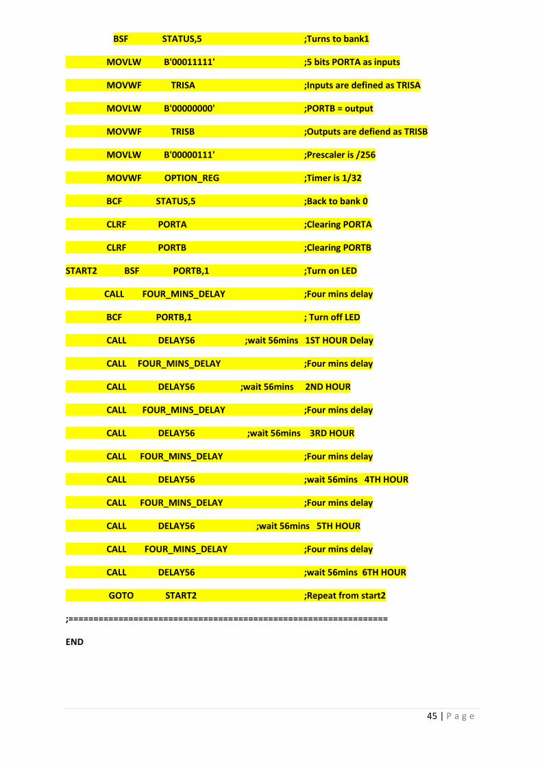
45 | P a g e
BSF STATUS,5 ;Turns to bank1
MOVLW B'00011111' ;5 bits PORTA as inputs
MOVWF TRISA ;Inputs are defined as TRISA
MOVLW B'00000000' ;PORTB = output
MOVWF TRISB ;Outputs are defiend as TRISB
MOVLW B'00000111' ;Prescaler is /256
MOVWF OPTION_REG ;Timer is 1/32
BCF STATUS,5 ;Back to bank 0
CLRF PORTA ;Clearing PORTA
CLRF PORTB ;Clearing PORTB
START2 BSF PORTB,1 ;Turn on LED
CALL FOUR_MINS_DELAY ;Four mins delay
BCF PORTB,1 ; Turn off LED
CALL DELAY56 ;wait 56mins 1ST HOUR Delay
CALL FOUR_MINS_DELAY ;Four mins delay
CALL DELAY56 ;wait 56mins 2ND HOUR
CALL FOUR_MINS_DELAY ;Four mins delay
CALL DELAY56 ;wait 56mins 3RD HOUR
CALL FOUR_MINS_DELAY ;Four mins delay
CALL DELAY56 ;wait 56mins 4TH HOUR
CALL FOUR_MINS_DELAY ;Four mins delay
CALL DELAY56 ;wait 56mins 5TH HOUR
CALL FOUR_MINS_DELAY ;Four mins delay
CALL DELAY56 ;wait 56mins 6TH HOUR
GOTO START2 ;Repeat from start2
;================================================================
END
46 | P a g e
Appendix 4 – Program Flow Chart
START
Delay 56(Mins)
Set LED on
Delay 4(Mins)
Call Delay 4(Mins)
Sub Routines
Set LED Off
Call Delay 56(Mins)
1 Hour Delay Achieved with LED
operating for 4 mins
Call Delay 4 and Delay 56, 4 more times in series to
make 6 Hours delay and repeat Cycle
Call Delay 4(Mins)
Call Delay 56(Mins)
1 hour Delay achieved, LED still
off
At this point LED has operated for 4 minutes & 6 hours
delay has been achieved. & Repeats


