Embed Size (px)
Citation preview
lable at ScienceDirect
Renewable Energy xxx (2014) 1e10
Contents lists avai
Renewable Energy
journal homepage: www.elsevier .com/locate/renene
High voltage step-up integrated double BoosteSepic DCeDC converterfor fuel-cell and photovoltaic applications
Ahmad J. Sabzali*, Esam H. Ismail, Hussain M. BehbehaniElectrical Engineering Department, College of Technological Studies, P.O. Box 35007, Al-Shaab 36051, Kuwait
a r t i c l e i n f o
Article history:Received 21 May 2014Accepted 12 August 2014Available online xxx
Keywords:Coupled inductorDCeDC power converterDouble boost converterHigh step-up converterLow current rippleSEPIC converter
* Corresponding author. Tel.: þ965 99709876; fax:E-mail addresses: [email protected], ahmadsabz
[email protected] (E.H. Ismail), [email protected]
http://dx.doi.org/10.1016/j.renene.2014.08.0340960-1481/© 2014 Elsevier Ltd. All rights reserved.
Please cite this article in press as: Sabzali Aphotovoltaic applications, Renewable Energ
a b s t r a c t
In this paper, an integrated double boost SEPIC (IDBS) converter is proposed as a high step-up converter.The proposed converter utilizes a single controlled power switch and two inductors and is able toprovide high voltage gain without extreme switch duty-cycle. The two inductors can be coupled into onecore for reducing the input current ripple without affecting the basic DC characteristic of the converter.Moreover, the voltage stresses across all the semiconductors are less than half of the output voltage. Thereduced voltage stress across the power switch enables the use of a lower voltage and RDS-ON MOSFETswitch, which will further reduce the conduction losses. Whereas, the low voltage stress across thediodes allows the use of Schottky rectifiers for alleviating the reverse-recovery current problem, leadingto a further reduction in the switching and conduction losses. A detailed circuit analysis is performed toderive the design equations. A design example for a 100-W/240 Vdc with 24 Vdc input voltage is provided.The feasibility of the converter is confirmed with results obtained from simulation and an experimentalprototype.
© 2014 Elsevier Ltd. All rights reserved.
1. Introduction
The world's demand for clean energy sources is growing rapidlyand it is driving research for the development of alternative energytechnologies. Among various renewable energy sources, wind en-ergy, photovoltaic (PV) cells, and fuel cells (FC) has gained signifi-cant momentum [1,2]. However, these renewable energy sourceshave low output voltage characteristics. Thus, due to their lowvoltage generation as well as high input current requirement, theydemand a high efficiency high step-up DCeDC converter to convertand regulate the low DC energy input source into suitable utiliza-tion voltage, current, and frequency for use by utility loads. Also, incase of PV and FC applications, it is required that the interfacedDCeDC converter injects small current ripple into the powersource. High current ripple magnitude reduces the energy extrac-ted from both the PV arrays and FC stack as well as it reduces thelifetime of the FC stack [3e5].
Practically, the conventional boost converter cannot provide avoltage gain greater than six times its applied voltage due toparasitic components associated with passive elements and
þ965 [email protected] (A.J. Sabzali),du.kw (H.M. Behbehani).
J, et al., High voltage step-uy (2014), http://dx.doi.org/10
semiconductor devices [6]. Also, the conventional boost converterrequires a high current and voltage rated MOSFET and diode whichleads to high conduction and switching losses. Cascading N con-ventional step-up converters using N number of controllableswitches [7e9] or by using a single controlled switch [10e12], canprovide a large step-up voltage conversion ratio without extremeduty-cycle operation. However, cascading topologies are not suit-able for high output voltage applications due to the high voltagestress across the power switch and the output rectifier which de-grades system conversion efficiency and increases size and cost.
Topologies based on coupled inductors techniques can producehigh voltage gain. However, besides their pulsating input current,but they require high voltage rated power switch due to the pres-ence of a resonant circuit between the leakage inductance of thecoupled inductor and the parasitic capacitor of the output diode[13,14]. An improved topology which reduces the effect of theleakage inductance on the active switch is proposed in Ref. [15].However, the switch current stress is high which limits the powerlevel improvements. The problem of the potential resonance be-tween the leakage inductance and the diode stray capacitor iscancelled in Ref. [16] by utilizing coupled inductor and voltagedoubler cell structure. Also, the circuit efficiency is further improvedby implementing zero-voltage-switching turn-on operation at theexpense of using two power switches which complicate the controlcircuit. However, the input current ripple is still high in Ref. [16].
p integrated double BoosteSepic DCeDC converter for fuel-cell and.1016/j.renene.2014.08.034
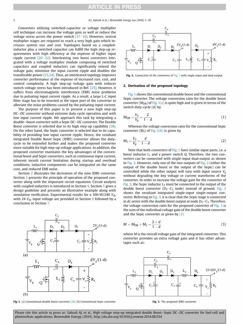
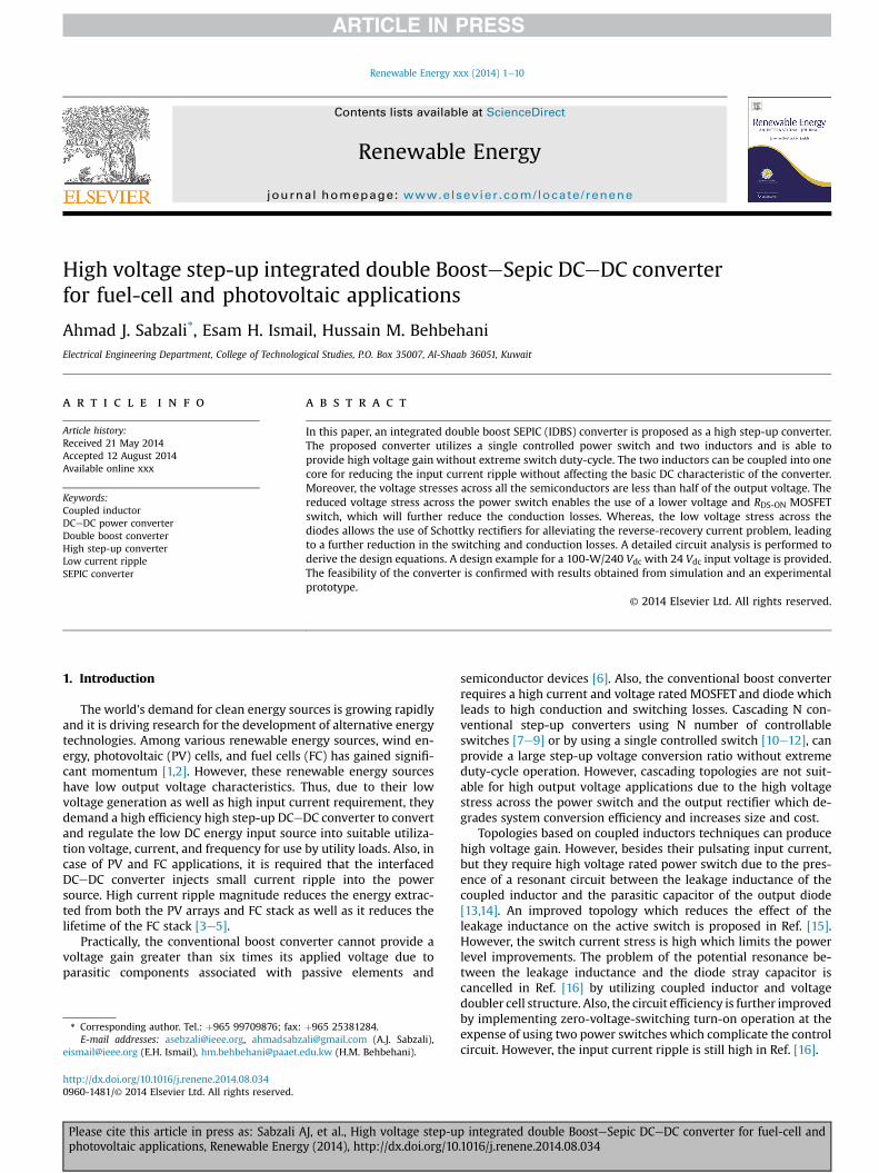
Fig. 2. Connection of the converters of Fig. 1 with single-input and dual-output.
A.J. Sabzali et al. / Renewable Energy xxx (2014) 1e102
Converters utilizing switched-capacitor or voltage multipliercell technique can increase the voltage gain as well as reduce thevoltage stress across the power switch [17e19]. However, severalmultiplier stages are required to reach a very high gain which in-creases system size and cost. Topologies based on a coupled-inductor plus a switched capacitor can fulfill the high step-up re-quirements with high efficiency at the expense of higher inputripple current [20e22]. Interleaving two boost converters inte-grated with a voltage multiplier module composing of switchedcapacitors and coupled inductors can significantly extend thevoltage gain, minimize the input current ripple and doubles thetransferable power [23,24]. Thus, an interleaved topology improvesconverter performance at the expense of increased size, cost, andcontrol complexity. A high step-up voltage gain with reducesswitch voltage stress has been introduced in Ref. [25]. However, itsuffers from electromagnetic interference (EMI) noise problemsdue to pulsating input current ripple. As a result, a large L-C inputfilter stage has to be inserted at the input port of the converter toalleviate the noise problems caused by the pulsating input current.
The purpose of this paper is to present a new high step-upDCeDC converter without extreme duty-cycle operation and withlow input current ripple. We approach this task by integrating adoubleeboost converter with a Sepic DCeDC converter. The DoubleBoost converter is selected due to its high step-up capability [18].On the other hand, the Sepic converter is selected due to its capa-bility of providing low input current ripple. Hence, the resultantintegrated Double Boost Sepic (IDBS) converter allows the duty-cycle to be extended further and makes the proposed convertermore suitable for high step-up voltage applications. In addition, theproposed converter maintains the key advantages of the conven-tional boost and Sepic converters, such as continuous input current,inherent inrush current limitation during startup and overloadconditions, inductive components can be integrated on the samecore, and reduced EMI noise.
Section 2 illustrates the derivation of the new IDBS converter.Section 3 presents the principle of operation of the proposed con-verter along with the important circuit equations. Circuit analysiswith coupled inductors is introduced in Section 4. Section 5 gives adesign guideline and presents an illustrative example along withsimulation verification. Experimental results for a 100-W/240 Vdcwith 24 Vdc input voltage are provided in Section 6 followed by aconclusion in Section 7.
Fig. 1. (a) Conventional double boost converter [18]. (b) Conventional Sepic converter.
Please cite this article in press as: Sabzali AJ, et al., High voltage step-uphotovoltaic applications, Renewable Energy (2014), http://dx.doi.org/10
2. Derivation of the proposed topology
Fig.1 shows the conventional double boost and the conventionalSepic converter. The voltage conversion ratio for the double boostconverter (MDB) of Fig. 1(a) is quite high and is given in terms of theswitch duty-cycle (d) by
MDB ¼ Vo
Vg¼ 2
1� d(1)
Whereas the voltage conversion ratio for the conventional Sepicconverter (MS) of Fig. 1(b) is given by
MS ¼Vo
Vg¼ d
1� d(2)
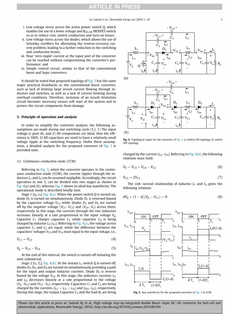
Note that both converters of Fig. 1 have similar input parts, i.e. aboost inductor L1 and a power switch Q. Therefore, the two con-verters can be connected with single-input dual-output as shownin Fig. 2. However, only one of the two outputs of Fig. 2 (either theoutput of the double boost or the output of the Sepic) can becontrolled while the other output will vary with input source Vgwithout degrading the key voltage or current waveforms of theconverter. In order to increase the voltage gain for the converter ofFig. 2, the Sepic inductor L2 must be connected to the output of thedouble boost converter (D3eC3 node) instead of ground. Fig. 3shows the resultant integrated single-input single-output con-verter. Referring to Fig. 3, it is clear that the Sepic stage is connectedin dc series with the double boost output at node D3eC3. Therefore,the voltage conversion ratio for the proposed converter of Fig. 3 isthe sum of the individual voltage gain of the double boost converterand the Sepic converter as given by (3)
M ¼ MDB þMS ¼2þ d1� d
(3)
whereM is the overall voltage gain of the integrated converter. Thisconverter provides an extra voltage gain and it has other advan-tages such as:
Fig. 3. The proposed IDBS converter.
p integrated double BoosteSepic DCeDC converter for fuel-cell and.1016/j.renene.2014.08.034
A.J. Sabzali et al. / Renewable Energy xxx (2014) 1e10 3
i. Low voltage stress across the active power switch Q, whichenables the use of a lower voltage and RDS-ON MOSFET switchso as to reduce cost, switch conduction and turn-on losses;
ii. Low voltage stress across the diodes, which allows the use ofSchottky rectifiers for alleviating the reverse-recovery cur-rent problem, leading to a further reduction in the switchingand conduction losses;
iii. Near ‘zero-ripple’ current at the input port of the convertercan be reached without compromising the converter's per-formance; and
iv. Simple control circuit, similar to that of the conventionalboost and Sepic converters.
It should be noted that proposed topology of Fig. 3 has the samemajor practical drawbacks as the conventional boost converter,such as lack of limiting large inrush current flowing through in-ductors and switches, as well as a lack of current limiting duringoverload conditions. Therefore, inclusion of an inrush limitationcircuit becomes necessary ensure soft start of the system and toprotect the circuit components from damage.
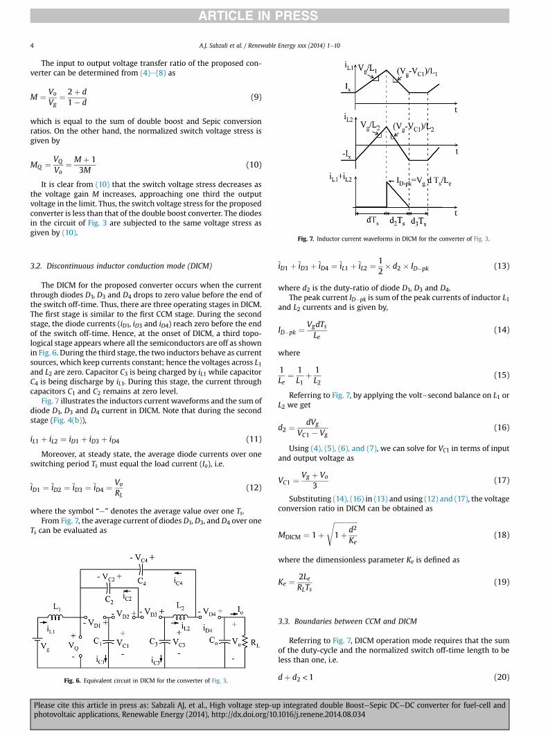
Fig. 4. Topological stages for the converter of Fig. 3. a) Switch ON topology, b) switchOFF topology.
3. Principle of operation and analysis
In order to simplify the converter analysis, the following as-sumptions are made during one switching cycle (Ts): 1) The inputvoltage is pure dc, and 2) All components are ideal, thus the effi-ciency is 100%. 3) All capacitors are sized to have a relatively smallvoltage ripple at the switching frequency. Under these assump-tions, a detailed analysis for the proposed converter of Fig. 3 isprovided next.
Fig. 5. Key waveforms for the proposed converter of Fig. 3 in CCM.
3.1. Continuous conduction mode (CCM)
Referring to Fig. 3, when the converter operates in the contin-uous conduction mode (CCM), the current ripples through the in-ductors L1 and L2 can be assumed negligible. Accordingly, the circuitoperation in one Ts can be divided into two stages as shown inFig. 4(a) and (b), whereas Fig. 5 shows its ideal key waveforms. Theoperational mode is described briefly next.
Stage 1 [t0, t1], Fig. 4(a): When the power switch Q is turned on,diode D2 is turned on simultaneously. Diode D1 is reversed-biasedby the capacitor voltage VC1, while diodes D3 and D4 are turnedoff by the negative voltage (VC1�VC3) and (VC4�Vo) across them,respectively. In this stage, the currents through the two inductorsincreases linearly at a rate proportional to the input voltage Vg.Capacitor C1 charges capacitor C2 while capacitor C4 is beingcharged by inductor L2 (iL2). Referring to Fig. 4(a), the voltage acrosscapacitor C1 and C2 are equal, while the difference between thecapacitors' voltages VC3 and VC4 must equal to the input voltage, i.e.,
VC1 ¼ VC2 (4)
Vg ¼ VC3 � VC4 (5)
At the end of this interval, the switch is turned-off initiating thenext subinterval.
Stage 2 [t1, Ts], Fig. 4(b): At the instant t1, switch Q is turned off,diodesD1, D3, and D4 are turned on simultaneously providing a pathfor the input and output inductor currents. Diode D2 is reversebiased by the voltage VC2. In this stage, the inductors currents iL1and iL2 decreases linearly at a rate proportional to the voltage(Vg�VC1) and (VC3�Vo), respectively. Capacitors C1 and C3 are beingcharged by the currents (iL1 þ iC2 þ iC4) and (iD3�iL2), respectively.During this stage, the output Capacitor Co and the load RL are being
Please cite this article in press as: Sabzali AJ, et al., High voltage step-uphotovoltaic applications, Renewable Energy (2014), http://dx.doi.org/10
charged by the current (iL2�iC4). Referring to Fig. 4(b), the followingrelations must hold:
Vo ¼ VC3 þ VC4 � VC2 (6)
VC3 ¼ 2VC1 (7)
The voltesecond relationship of inductor L1 and L2 gives thefollowing relations
dVg þ�1� d
��Vg � VC1
� ¼ 0 (8)
p integrated double BoosteSepic DCeDC converter for fuel-cell and.1016/j.renene.2014.08.034
A.J. Sabzali et al. / Renewable Energy xxx (2014) 1e104
The input to output voltage transfer ratio of the proposed con-verter can be determined from (4)e(8) as
M ¼ Vo
Vg¼ 2þ d
1� d(9)
which is equal to the sum of double boost and Sepic conversionratios. On the other hand, the normalized switch voltage stress isgiven by
MQ ¼ VQ
Vo¼ M þ 1
3M(10)
It is clear from (10) that the switch voltage stress decreases asthe voltage gain M increases, approaching one third the outputvoltage in the limit. Thus, the switch voltage stress for the proposedconverter is less than that of the double boost converter. The diodesin the circuit of Fig. 3 are subjected to the same voltage stress asgiven by (10).
Fig. 7. Inductor current waveforms in DICM for the converter of Fig. 3.
3.2. Discontinuous inductor conduction mode (DICM)
The DICM for the proposed converter occurs when the currentthrough diodes D1, D3 and D4 drops to zero value before the end ofthe switch off-time. Thus, there are three operating stages in DICM.The first stage is similar to the first CCM stage. During the secondstage, the diode currents (iD1, iD3 and iD4) reach zero before the endof the switch off-time. Hence, at the onset of DICM, a third topo-logical stage appears where all the semiconductors are off as shownin Fig. 6. During the third stage, the two inductors behave as currentsources, which keep currents constant; hence the voltages across L1and L2 are zero. Capacitor C3 is being charged by iL1 while capacitorC4 is being discharge by iL1. During this stage, the current throughcapacitors C1 and C2 remains at zero level.
Fig. 7 illustrates the inductors current waveforms and the sum ofdiode D1, D3 and D4 current in DICM. Note that during the secondstage (Fig. 4(b)),
iL1 þ iL2 ¼ iD1 þ iD3 þ iD4 (11)
Moreover, at steady state, the average diode currents over oneswitching period Ts must equal the load current (Io), i.e.
iD1 ¼ iD2 ¼ iD3 ¼ iD4 ¼ Vo
RL(12)
where the symbol “�” denotes the average value over one Ts.From Fig. 7, the average current of diodes D1, D3, and D4 over one
Ts can be evaluated as
Fig. 6. Equivalent circuit in DICM for the converter of Fig. 3.
Please cite this article in press as: Sabzali AJ, et al., High voltage step-uphotovoltaic applications, Renewable Energy (2014), http://dx.doi.org/10
iD1 þ iD3 þ iD4 ¼ iL1 þ iL2 ¼ 12� d2 � ID�pk (13)
where d2 is the duty-ratio of diode D1, D3 and D4.The peak current ID�pk is sum of the peak currents of inductor L1
and L2 currents and is given by,
ID�pk ¼VgdTsLe
(14)
where
1Le
¼ 1L1
þ 1L2
(15)
Referring to Fig. 7, by applying the voltesecond balance on L1 orL2 we get
d2 ¼ dVg
VC1 � Vg(16)
Using (4), (5), (6), and (7), we can solve for VC1 in terms of inputand output voltage as
VC1 ¼ Vg þ Vo
3(17)
Substituting (14), (16) in (13) and using (12) and (17), the voltageconversion ratio in DICM can be obtained as
MDICM ¼ 1þffiffiffiffiffiffiffiffiffiffiffiffiffiffi1þ d2
Ke
s(18)
where the dimensionless parameter Ke is defined as
Ke ¼ 2LeRLTs
(19)
3.3. Boundaries between CCM and DICM
Referring to Fig. 7, DICM operation mode requires that the sumof the duty-cycle and the normalized switch off-time length to beless than one, i.e.
dþ d2 <1 (20)
p integrated double BoosteSepic DCeDC converter for fuel-cell and.1016/j.renene.2014.08.034
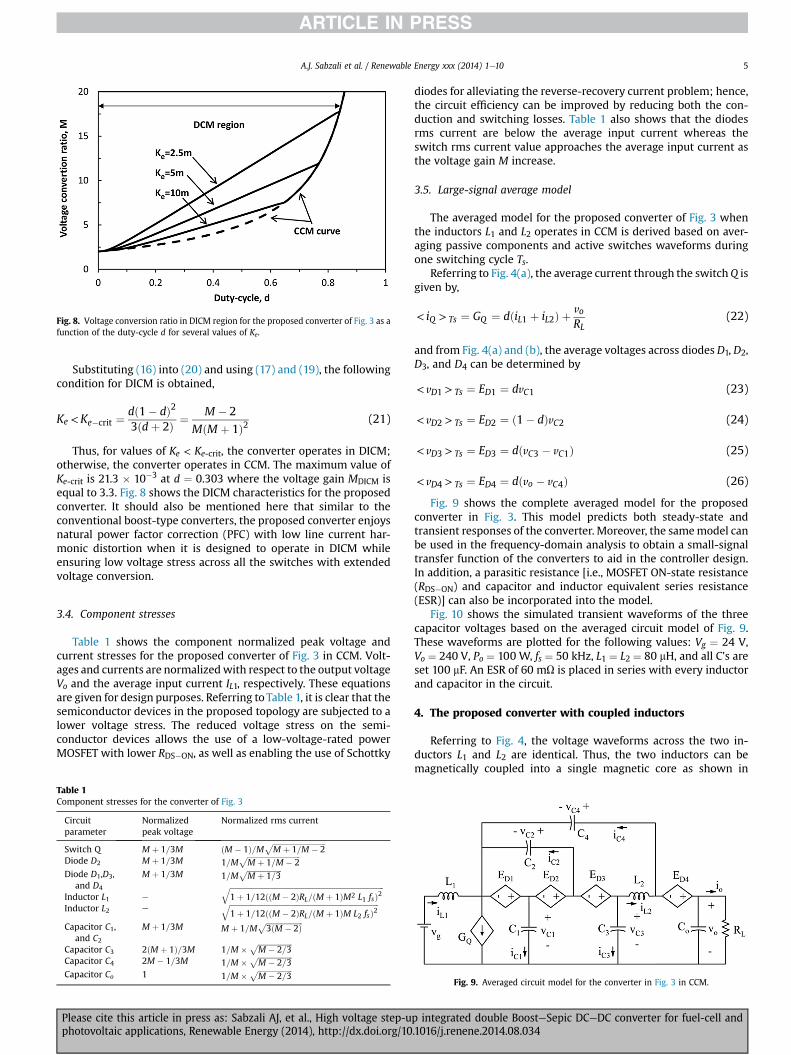
Fig. 8. Voltage conversion ratio in DICM region for the proposed converter of Fig. 3 as afunction of the duty-cycle d for several values of Ke.
A.J. Sabzali et al. / Renewable Energy xxx (2014) 1e10 5
Substituting (16) into (20) and using (17) and (19), the followingcondition for DICM is obtained,
Ke <Ke�crit ¼dð1� dÞ23ðdþ 2Þ ¼ M � 2
MðM þ 1Þ2(21)
Thus, for values of Ke < Ke-crit, the converter operates in DICM;otherwise, the converter operates in CCM. The maximum value ofKe-crit is 21.3 � 10�3 at d ¼ 0.303 where the voltage gain MDICM isequal to 3.3. Fig. 8 shows the DICM characteristics for the proposedconverter. It should also be mentioned here that similar to theconventional boost-type converters, the proposed converter enjoysnatural power factor correction (PFC) with low line current har-monic distortion when it is designed to operate in DICM whileensuring low voltage stress across all the switches with extendedvoltage conversion.
3.4. Component stresses
Table 1 shows the component normalized peak voltage andcurrent stresses for the proposed converter of Fig. 3 in CCM. Volt-ages and currents are normalizedwith respect to the output voltageVo and the average input current IL1, respectively. These equationsare given for design purposes. Referring toTable 1, it is clear that thesemiconductor devices in the proposed topology are subjected to alower voltage stress. The reduced voltage stress on the semi-conductor devices allows the use of a low-voltage-rated powerMOSFET with lower RDS�ON, as well as enabling the use of Schottky
Table 1Component stresses for the converter of Fig. 3
Circuitparameter
Normalizedpeak voltage
Normalized rms current
Switch Q M þ 1=3M ðM � 1Þ=M ffiffiffiffiffiffiffiffiffiffiffiffiffiffiffiffiffiffiffiffiffiffiffiffiffiffiffiffiffiM þ 1=M � 2
pDiode D2 M þ 1=3M 1=M
ffiffiffiffiffiffiffiffiffiffiffiffiffiffiffiffiffiffiffiffiffiffiffiffiffiffiffiffiffiM þ 1=M � 2
pDiode D1,D3,
and D4
M þ 1=3M 1=MffiffiffiffiffiffiffiffiffiffiffiffiffiffiffiffiffiffiffiM þ 1=3
pInductor L1 e
ffiffiffiffiffiffiffiffiffiffiffiffiffiffiffiffiffiffiffiffiffiffiffiffiffiffiffiffiffiffiffiffiffiffiffiffiffiffiffiffiffiffiffiffiffiffiffiffiffiffiffiffiffiffiffiffiffiffiffiffiffiffiffiffiffiffiffiffiffiffiffiffiffiffiffiffiffiffiffiffiffiffiffiffi1þ 1=12ððM � 2ÞRL=ðM þ 1ÞM2 L1 fsÞ2
qInductor L2 e
ffiffiffiffiffiffiffiffiffiffiffiffiffiffiffiffiffiffiffiffiffiffiffiffiffiffiffiffiffiffiffiffiffiffiffiffiffiffiffiffiffiffiffiffiffiffiffiffiffiffiffiffiffiffiffiffiffiffiffiffiffiffiffiffiffiffiffiffiffiffiffiffiffiffiffiffiffiffiffiffiffi1þ 1=12ððM � 2ÞRL=ðM þ 1ÞM L2 fsÞ2
qCapacitor C1,
and C2
M þ 1=3M M þ 1=Mffiffiffiffiffiffiffiffiffiffiffiffiffiffiffiffiffiffiffiffi3ðM � 2Þp
Capacitor C3 2ðM þ 1Þ=3M 1=M � ffiffiffiffiffiffiffiffiffiffiffiffiffiffiffiffiffiffiffiM � 2=3
pCapacitor C4 2M � 1=3M 1=M � ffiffiffiffiffiffiffiffiffiffiffiffiffiffiffiffiffiffiffi
M � 2=3p
Capacitor Co 1 1=M � ffiffiffiffiffiffiffiffiffiffiffiffiffiffiffiffiffiffiffiM � 2=3
p
Please cite this article in press as: Sabzali AJ, et al., High voltage step-uphotovoltaic applications, Renewable Energy (2014), http://dx.doi.org/10
diodes for alleviating the reverse-recovery current problem; hence,the circuit efficiency can be improved by reducing both the con-duction and switching losses. Table 1 also shows that the diodesrms current are below the average input current whereas theswitch rms current value approaches the average input current asthe voltage gain M increase.
3.5. Large-signal average model
The averaged model for the proposed converter of Fig. 3 whenthe inductors L1 and L2 operates in CCM is derived based on aver-aging passive components and active switches waveforms duringone switching cycle Ts.
Referring to Fig. 4(a), the average current through the switchQ isgiven by,
< iQ > Ts ¼ GQ ¼ dðiL1 þ iL2Þ þvoRL
(22)
and from Fig. 4(a) and (b), the average voltages across diodes D1, D2,D3, and D4 can be determined by
< vD1 > Ts ¼ ED1 ¼ dvC1 (23)
< vD2 > Ts ¼ ED2 ¼ ð1� dÞvC2 (24)
< vD3 > Ts ¼ ED3 ¼ dðvC3 � vC1Þ (25)
< vD4 > Ts ¼ ED4 ¼ dðvo � vC4Þ (26)
Fig. 9 shows the complete averaged model for the proposedconverter in Fig. 3. This model predicts both steady-state andtransient responses of the converter. Moreover, the samemodel canbe used in the frequency-domain analysis to obtain a small-signaltransfer function of the converters to aid in the controller design.In addition, a parasitic resistance [i.e., MOSFET ON-state resistance(RDS�ON) and capacitor and inductor equivalent series resistance(ESR)] can also be incorporated into the model.
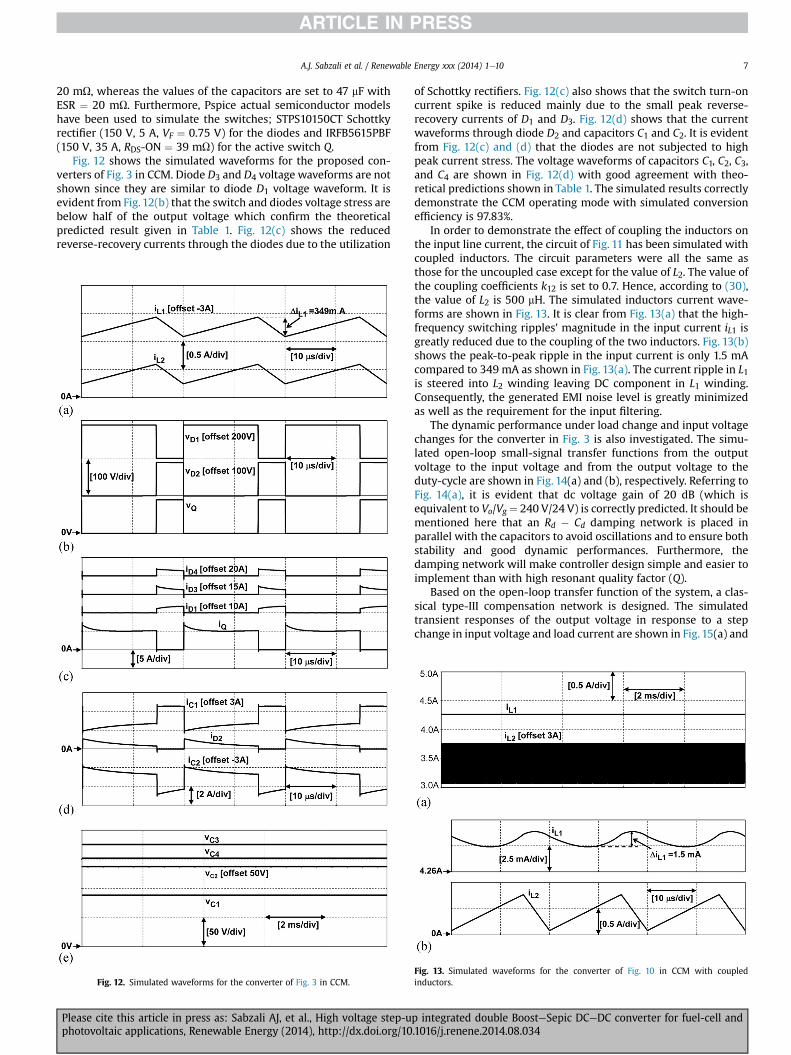
Fig. 10 shows the simulated transient waveforms of the threecapacitor voltages based on the averaged circuit model of Fig. 9.These waveforms are plotted for the following values: Vg ¼ 24 V,Vo ¼ 240 V, Po ¼ 100 W, fs ¼ 50 kHz, L1 ¼ L2 ¼ 80 mH, and all C's areset 100 mF. An ESR of 60 mU is placed in series with every inductorand capacitor in the circuit.
4. The proposed converter with coupled inductors
Referring to Fig. 4, the voltage waveforms across the two in-ductors L1 and L2 are identical. Thus, the two inductors can bemagnetically coupled into a single magnetic core as shown in
Fig. 9. Averaged circuit model for the converter in Fig. 3 in CCM.
p integrated double BoosteSepic DCeDC converter for fuel-cell and.1016/j.renene.2014.08.034
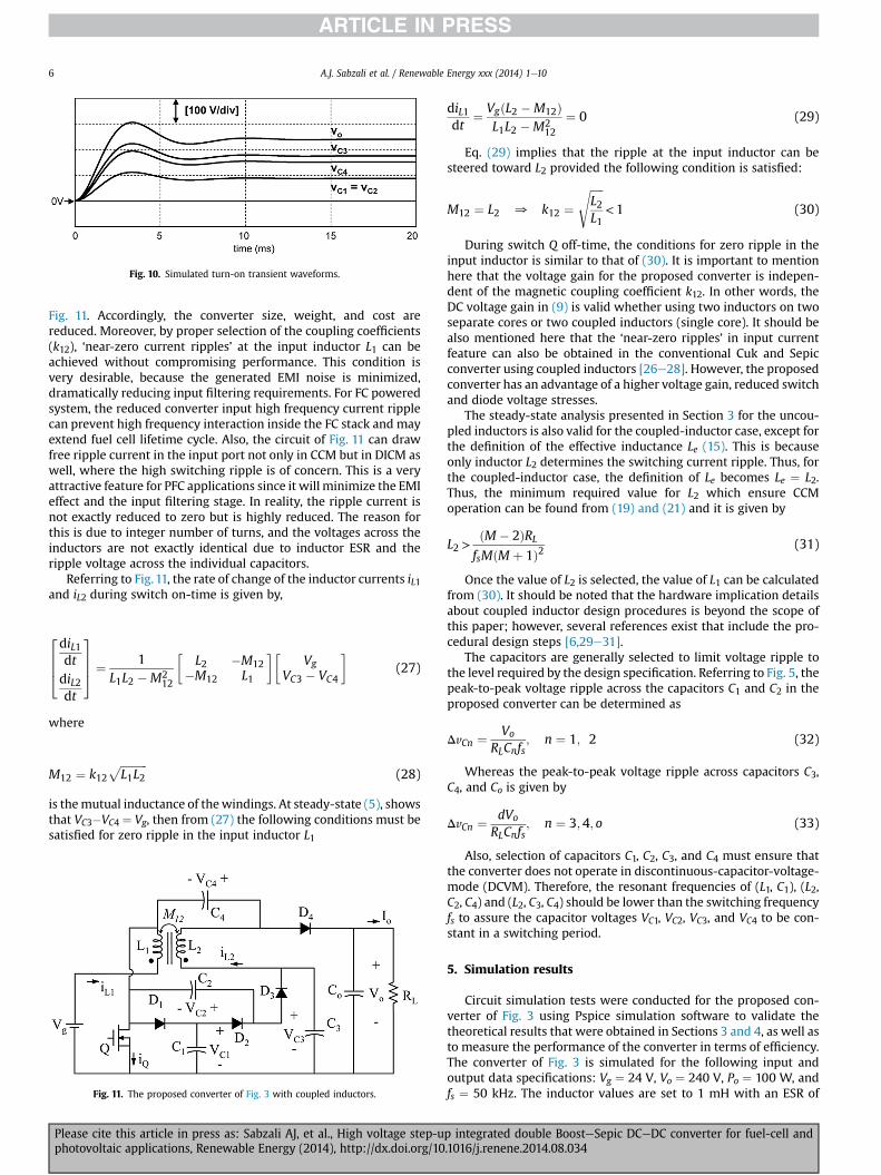
Fig. 10. Simulated turn-on transient waveforms.
A.J. Sabzali et al. / Renewable Energy xxx (2014) 1e106
Fig. 11. Accordingly, the converter size, weight, and cost arereduced. Moreover, by proper selection of the coupling coefficients(k12), ‘near-zero current ripples’ at the input inductor L1 can beachieved without compromising performance. This condition isvery desirable, because the generated EMI noise is minimized,dramatically reducing input filtering requirements. For FC poweredsystem, the reduced converter input high frequency current ripplecan prevent high frequency interaction inside the FC stack and mayextend fuel cell lifetime cycle. Also, the circuit of Fig. 11 can drawfree ripple current in the input port not only in CCM but in DICM aswell, where the high switching ripple is of concern. This is a veryattractive feature for PFC applications since it will minimize the EMIeffect and the input filtering stage. In reality, the ripple current isnot exactly reduced to zero but is highly reduced. The reason forthis is due to integer number of turns, and the voltages across theinductors are not exactly identical due to inductor ESR and theripple voltage across the individual capacitors.
Referring to Fig. 11, the rate of change of the inductor currents iL1and iL2 during switch on-time is given by,
2664diL1dtdiL2dt
3775 ¼ 1
L1L2 �M212
�L2 �M12
�M12 L1
��Vg
VC3 � VC4
�(27)
where
M12 ¼ k12ffiffiffiffiffiffiffiffiffiffiL1L2
p(28)
is themutual inductance of thewindings. At steady-state (5), showsthat VC3�VC4 ¼ Vg, then from (27) the following conditions must besatisfied for zero ripple in the input inductor L1
Fig. 11. The proposed converter of Fig. 3 with coupled inductors.
Please cite this article in press as: Sabzali AJ, et al., High voltage step-uphotovoltaic applications, Renewable Energy (2014), http://dx.doi.org/10
diL1dt
¼ VgðL2 �M12ÞL1L2 �M2
12
¼ 0 (29)
Eq. (29) implies that the ripple at the input inductor can besteered toward L2 provided the following condition is satisfied:
M12 ¼ L2 0 k12 ¼ffiffiffiffiffiL2L1
s<1 (30)
During switch Q off-time, the conditions for zero ripple in theinput inductor is similar to that of (30). It is important to mentionhere that the voltage gain for the proposed converter is indepen-dent of the magnetic coupling coefficient k12. In other words, theDC voltage gain in (9) is valid whether using two inductors on twoseparate cores or two coupled inductors (single core). It should bealso mentioned here that the ‘near-zero ripples’ in input currentfeature can also be obtained in the conventional Cuk and Sepicconverter using coupled inductors [26e28]. However, the proposedconverter has an advantage of a higher voltage gain, reduced switchand diode voltage stresses.
The steady-state analysis presented in Section 3 for the uncou-pled inductors is also valid for the coupled-inductor case, except forthe definition of the effective inductance Le (15). This is becauseonly inductor L2 determines the switching current ripple. Thus, forthe coupled-inductor case, the definition of Le becomes Le ¼ L2.Thus, the minimum required value for L2 which ensure CCMoperation can be found from (19) and (21) and it is given by
L2 >ðM � 2ÞRL
fsMðM þ 1Þ2(31)
Once the value of L2 is selected, the value of L1 can be calculatedfrom (30). It should be noted that the hardware implication detailsabout coupled inductor design procedures is beyond the scope ofthis paper; however, several references exist that include the pro-cedural design steps [6,29e31].
The capacitors are generally selected to limit voltage ripple tothe level required by the design specification. Referring to Fig. 5, thepeak-to-peak voltage ripple across the capacitors C1 and C2 in theproposed converter can be determined as
DvCn ¼ Vo
RLCnfs; n ¼ 1; 2 (32)
Whereas the peak-to-peak voltage ripple across capacitors C3,C4, and Co is given by
DvCn ¼ dVo
RLCnfs; n ¼ 3;4; o (33)
Also, selection of capacitors C1, C2, C3, and C4 must ensure thatthe converter does not operate in discontinuous-capacitor-voltage-mode (DCVM). Therefore, the resonant frequencies of (L1, C1), (L2,C2, C4) and (L2, C3, C4) should be lower than the switching frequencyfs to assure the capacitor voltages VC1, VC2, VC3, and VC4 to be con-stant in a switching period.
5. Simulation results
Circuit simulation tests were conducted for the proposed con-verter of Fig. 3 using Pspice simulation software to validate thetheoretical results that were obtained in Sections 3 and 4, as well asto measure the performance of the converter in terms of efficiency.The converter of Fig. 3 is simulated for the following input andoutput data specifications: Vg ¼ 24 V, Vo ¼ 240 V, Po ¼ 100 W, andfs ¼ 50 kHz. The inductor values are set to 1 mH with an ESR of
p integrated double BoosteSepic DCeDC converter for fuel-cell and.1016/j.renene.2014.08.034
A.J. Sabzali et al. / Renewable Energy xxx (2014) 1e10 7
20 mU, whereas the values of the capacitors are set to 47 mF withESR ¼ 20 mU. Furthermore, Pspice actual semiconductor modelshave been used to simulate the switches; STPS10150CT Schottkyrectifier (150 V, 5 A, VF ¼ 0.75 V) for the diodes and IRFB5615PBF(150 V, 35 A, RDS-ON ¼ 39 mU) for the active switch Q.
Fig. 12 shows the simulated waveforms for the proposed con-verters of Fig. 3 in CCM. Diode D3 and D4 voltage waveforms are notshown since they are similar to diode D1 voltage waveform. It isevident from Fig. 12(b) that the switch and diodes voltage stress arebelow half of the output voltage which confirm the theoreticalpredicted result given in Table 1. Fig. 12(c) shows the reducedreverse-recovery currents through the diodes due to the utilization
Fig. 12. Simulated waveforms for the converter of Fig. 3 in CCM.
Please cite this article in press as: Sabzali AJ, et al., High voltage step-uphotovoltaic applications, Renewable Energy (2014), http://dx.doi.org/10
of Schottky rectifiers. Fig. 12(c) also shows that the switch turn-oncurrent spike is reduced mainly due to the small peak reverse-recovery currents of D1 and D3. Fig. 12(d) shows that the currentwaveforms through diode D2 and capacitors C1 and C2. It is evidentfrom Fig. 12(c) and (d) that the diodes are not subjected to highpeak current stress. The voltage waveforms of capacitors C1, C2, C3,and C4 are shown in Fig. 12(d) with good agreement with theo-retical predictions shown in Table 1. The simulated results correctlydemonstrate the CCM operating mode with simulated conversionefficiency is 97.83%.
In order to demonstrate the effect of coupling the inductors onthe input line current, the circuit of Fig. 11 has been simulated withcoupled inductors. The circuit parameters were all the same asthose for the uncoupled case except for the value of L2. The value ofthe coupling coefficients k12 is set to 0.7. Hence, according to (30),the value of L2 is 500 mH. The simulated inductors current wave-forms are shown in Fig. 13. It is clear from Fig. 13(a) that the high-frequency switching ripples' magnitude in the input current iL1 isgreatly reduced due to the coupling of the two inductors. Fig. 13(b)shows the peak-to-peak ripple in the input current is only 1.5 mAcompared to 349 mA as shown in Fig. 13(a). The current ripple in L1is steered into L2 winding leaving DC component in L1 winding.Consequently, the generated EMI noise level is greatly minimizedas well as the requirement for the input filtering.
The dynamic performance under load change and input voltagechanges for the converter in Fig. 3 is also investigated. The simu-lated open-loop small-signal transfer functions from the outputvoltage to the input voltage and from the output voltage to theduty-cycle are shown in Fig. 14(a) and (b), respectively. Referring toFig. 14(a), it is evident that dc voltage gain of 20 dB (which isequivalent to Vo/Vg¼ 240 V/24 V) is correctly predicted. It should bementioned here that an Rd � Cd damping network is placed inparallel with the capacitors to avoid oscillations and to ensure bothstability and good dynamic performances. Furthermore, thedamping network will make controller design simple and easier toimplement than with high resonant quality factor (Q).
Based on the open-loop transfer function of the system, a clas-sical type-III compensation network is designed. The simulatedtransient responses of the output voltage in response to a stepchange in input voltage and load current are shown in Fig. 15(a) and
Fig. 13. Simulated waveforms for the converter of Fig. 10 in CCM with coupledinductors.
p integrated double BoosteSepic DCeDC converter for fuel-cell and.1016/j.renene.2014.08.034
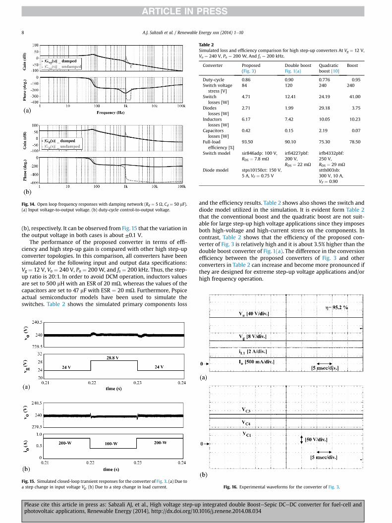
Fig. 14. Open loop frequency responses with damping network (Rd ¼ 5 U, Cd ¼ 50 mF).(a) Input voltage-to-output voltage. (b) duty-cycle control-to-output voltage.
Table 2Simulated loss and efficiency comparison for high step-up converters At Vg ¼ 12 V,Vo ¼ 240 V, Po ¼ 200 W, And fs ¼ 200 kHz.
Converter Proposed(Fig. 3)
Double boostFig. 1(a)
Quadraticboost [10]
Boost
Duty-cycle 0.86 0.90 0.776 0.95Switch voltage
stress [V]84 120 240 240
Switchlosses [W]
4.71 12.41 24.19 41.00
Diodeslosses [W]
2.71 1.99 29.18 3.75
Inductorslosses [W]
6.17 7.42 10.05 10.23
Capacitorslosses [W]
0.42 0.15 2.19 0.07
Full-loadefficiency [%]
93.50 90.10 75.30 78.50
Switch model sir846adp: 100 V,RDS ¼ 7.8 mU
irfi4227pbf:200 V,RDS ¼ 22 mU
irfb4332pbf:250 V,RDS ¼ 29 mU
Diode model stps10150ct: 150 V,5 A, VF ¼ 0.75 V
stth003sb:300 V, 10 A,VF ¼ 0.90
A.J. Sabzali et al. / Renewable Energy xxx (2014) 1e108
(b), respectively. It can be observed from Fig. 15 that the variation inthe output voltage in both cases is about ±0.1 V.
The performance of the proposed converter in terms of effi-ciency and high step-up gain is compared with other high step-upconverter topologies. In this comparison, all converters have beensimulated for the following input and output data specifications:Vg ¼ 12 V, Vo ¼ 240 V, Po ¼ 200W, and fs ¼ 200 kHz. Thus, the step-up ratio is 20:1. In order to avoid DCM operation, inductors valuesare set to 500 mH with an ESR of 20 mU, whereas the values of thecapacitors are set to 47 mF with ESR ¼ 20 mU. Furthermore, Pspiceactual semiconductor models have been used to simulate theswitches. Table 2 shows the simulated primary components loss
Fig. 15. Simulated closed-loop transient responses for the converter of Fig. 3. (a) Due toa step change in input voltage Vg. (b) Due to a step change in load current.
Please cite this article in press as: Sabzali AJ, et al., High voltage step-uphotovoltaic applications, Renewable Energy (2014), http://dx.doi.org/10
and the efficiency results. Table 2 shows also shows the switch anddiode model utilized in the simulation. It is evident form Table 2that the conventional boost and the quadratic boost are not suit-able for large step-up high voltage applications since they imposesboth high-voltage and high-current stress on the components. Incontrast, Table 2 shows that the efficiency of the proposed con-verter of Fig. 3 is relatively high and it is about 3.5% higher than thedouble boost converter of Fig. 1(a). The difference in the conversionefficiency between the proposed converters of Fig. 3 and otherconverters in Table 2 can increase and become more pronounced ifthey are designed for extreme step-up voltage applications and/orhigh frequency operation.
Fig. 16. Experimental waveforms for the converter of Fig. 3.
p integrated double BoosteSepic DCeDC converter for fuel-cell and.1016/j.renene.2014.08.034
A.J. Sabzali et al. / Renewable Energy xxx (2014) 1e10 9
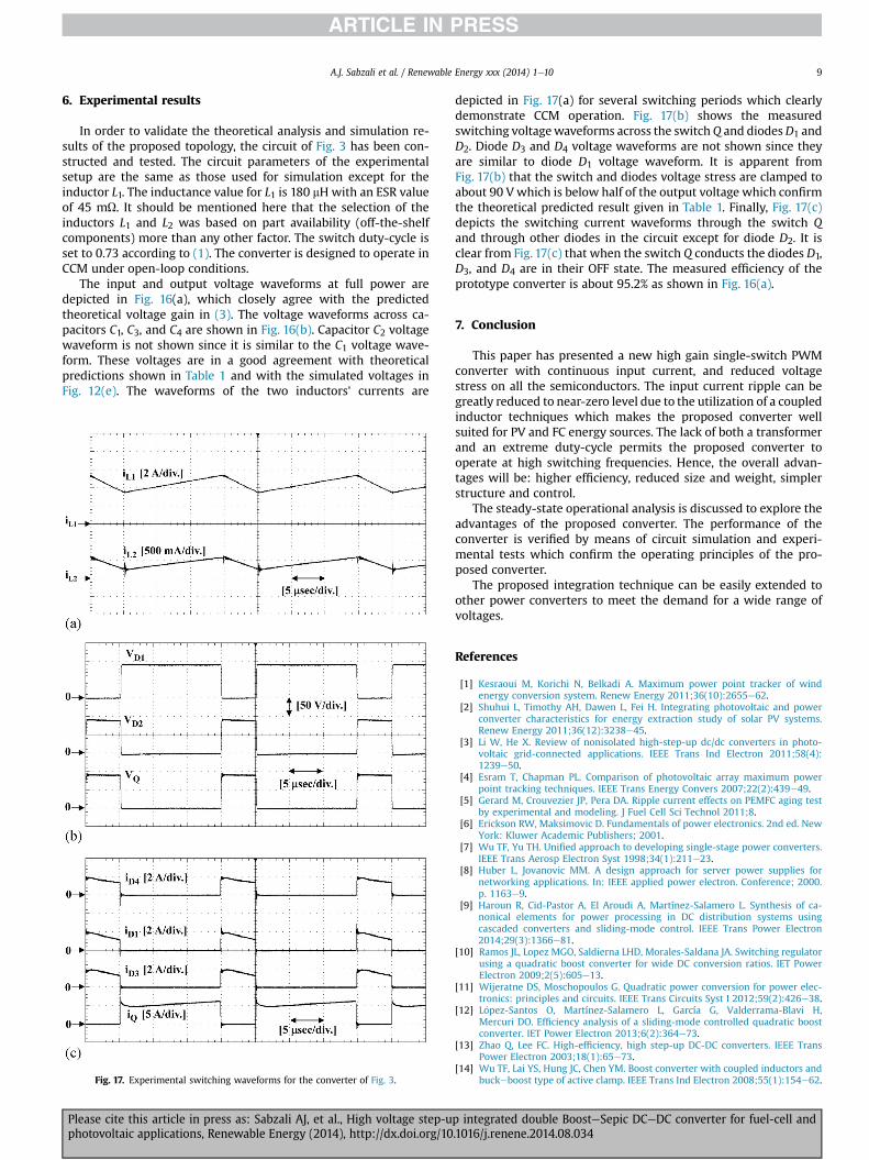
6. Experimental results
In order to validate the theoretical analysis and simulation re-sults of the proposed topology, the circuit of Fig. 3 has been con-structed and tested. The circuit parameters of the experimentalsetup are the same as those used for simulation except for theinductor L1. The inductance value for L1 is 180 mH with an ESR valueof 45 mU. It should be mentioned here that the selection of theinductors L1 and L2 was based on part availability (off-the-shelfcomponents) more than any other factor. The switch duty-cycle isset to 0.73 according to (1). The converter is designed to operate inCCM under open-loop conditions.
The input and output voltage waveforms at full power aredepicted in Fig. 16(a), which closely agree with the predictedtheoretical voltage gain in (3). The voltage waveforms across ca-pacitors C1, C3, and C4 are shown in Fig. 16(b). Capacitor C2 voltagewaveform is not shown since it is similar to the C1 voltage wave-form. These voltages are in a good agreement with theoreticalpredictions shown in Table 1 and with the simulated voltages inFig. 12(e). The waveforms of the two inductors' currents are
Fig. 17. Experimental switching waveforms for the converter of Fig. 3.
Please cite this article in press as: Sabzali AJ, et al., High voltage step-uphotovoltaic applications, Renewable Energy (2014), http://dx.doi.org/10
depicted in Fig. 17(a) for several switching periods which clearlydemonstrate CCM operation. Fig. 17(b) shows the measuredswitching voltagewaveforms across the switch Q and diodesD1 andD2. Diode D3 and D4 voltage waveforms are not shown since theyare similar to diode D1 voltage waveform. It is apparent fromFig. 17(b) that the switch and diodes voltage stress are clamped toabout 90 V which is below half of the output voltage which confirmthe theoretical predicted result given in Table 1. Finally, Fig. 17(c)depicts the switching current waveforms through the switch Qand through other diodes in the circuit except for diode D2. It isclear from Fig. 17(c) that when the switch Q conducts the diodes D1,D3, and D4 are in their OFF state. The measured efficiency of theprototype converter is about 95.2% as shown in Fig. 16(a).
7. Conclusion
This paper has presented a new high gain single-switch PWMconverter with continuous input current, and reduced voltagestress on all the semiconductors. The input current ripple can begreatly reduced to near-zero level due to the utilization of a coupledinductor techniques which makes the proposed converter wellsuited for PV and FC energy sources. The lack of both a transformerand an extreme duty-cycle permits the proposed converter tooperate at high switching frequencies. Hence, the overall advan-tages will be: higher efficiency, reduced size and weight, simplerstructure and control.
The steady-state operational analysis is discussed to explore theadvantages of the proposed converter. The performance of theconverter is verified by means of circuit simulation and experi-mental tests which confirm the operating principles of the pro-posed converter.
The proposed integration technique can be easily extended toother power converters to meet the demand for a wide range ofvoltages.
References
[1] Kesraoui M, Korichi N, Belkadi A. Maximum power point tracker of windenergy conversion system. Renew Energy 2011;36(10):2655e62.
[2] Shuhui L, Timothy AH, Dawen L, Fei H. Integrating photovoltaic and powerconverter characteristics for energy extraction study of solar PV systems.Renew Energy 2011;36(12):3238e45.
[3] Li W, He X. Review of nonisolated high-step-up dc/dc converters in photo-voltaic grid-connected applications. IEEE Trans Ind Electron 2011;58(4):1239e50.
[4] Esram T, Chapman PL. Comparison of photovoltaic array maximum powerpoint tracking techniques. IEEE Trans Energy Convers 2007;22(2):439e49.
[5] Gerard M, Crouvezier JP, Pera DA. Ripple current effects on PEMFC aging testby experimental and modeling. J Fuel Cell Sci Technol 2011;8.
[6] Erickson RW, Maksimovic D. Fundamentals of power electronics. 2nd ed. NewYork: Kluwer Academic Publishers; 2001.
[7] Wu TF, Yu TH. Unified approach to developing single-stage power converters.IEEE Trans Aerosp Electron Syst 1998;34(1):211e23.
[8] Huber L, Jovanovic MM. A design approach for server power supplies fornetworking applications. In: IEEE applied power electron. Conference; 2000.p. 1163e9.
[9] Haroun R, Cid-Pastor A, El Aroudi A, Martínez-Salamero L. Synthesis of ca-nonical elements for power processing in DC distribution systems usingcascaded converters and sliding-mode control. IEEE Trans Power Electron2014;29(3):1366e81.
[10] Ramos JL, Lopez MGO, Saldierna LHD, Morales-Saldana JA. Switching regulatorusing a quadratic boost converter for wide DC conversion ratios. IET PowerElectron 2009;2(5):605e13.
[11] Wijeratne DS, Moschopoulos G. Quadratic power conversion for power elec-tronics: principles and circuits. IEEE Trans Circuits Syst I 2012;59(2):426e38.
[12] L�opez-Santos O, Martínez-Salamero L, García G, Valderrama-Blavi H,Mercuri DO. Efficiency analysis of a sliding-mode controlled quadratic boostconverter. IET Power Electron 2013;6(2):364e73.
[13] Zhao Q, Lee FC. High-efficiency, high step-up DC-DC converters. IEEE TransPower Electron 2003;18(1):65e73.
[14] Wu TF, Lai YS, Hung JC, Chen YM. Boost converter with coupled inductors andbuckeboost type of active clamp. IEEE Trans Ind Electron 2008;55(1):154e62.
p integrated double BoosteSepic DCeDC converter for fuel-cell and.1016/j.renene.2014.08.034

A.J. Sabzali et al. / Renewable Energy xxx (2014) 1e1010
[15] Chen SM, Liang TJ, Yang LS, Chen JF. A cascaded high step-up DCeDC con-verter with single switch for microsource applications. IEEE Trans PowerElectron 2011;26(4):1146e53.
[16] Zhao Y, Li W, He X. Single-phase improved active clamp coupled-inductor-based converter with extended voltage doubler cell. IEEE Trans Power Elec-tron 2012;27(6):2869e78.
[17] Ismail EH, Al-SaffarMA, Sabzali AJ. High conversion ratio dcedc converterswithreduced switch stress. IEEE Trans Circuits Syst I Reg Pap 2008;55(7):2139e51.
[18] Prudente M, Pfitscher LL, Emmendoerfer G, Romaneli EF, Gules R. Voltagemultiplier cells applied to non-isolated DC-DC converters. IEEE Trans PowerElectron 2008;23(2):871e87.
[19] Young CM, Chen MH, Chang TA, Ko CC, Jen KK. Cascade CockcrofteWaltonvoltage multiplier applied to transformerless high step-up DCeDC converter.IEEE Trans Ind Electron 2013;60(2):523e37.
[20] Liang TJ, Chen SM, Yang LS, Chen JF, Ioinovici A. Ultra-large gain step-upswitched-capacitor DC-DC converter with coupled inductor for alternativesources of energy. IEEE Trans Circuit Syst I Reg Pap 2012;59(4):864e74.
[21] Hsieh YP, Chen JF, Liang TJ, Yang LS. Analysis and implementation of a novelsingle-switch high step-up DC-DC converter. IET Power Electron 2012;5(1):11e21.
[22] Hu X, Gong C. A high voltage gain DCeDC converter integrating coupled-inductor and diodeecapacitor techniques. IEEE Trans Power Electron2014;29(2):789e800.
Please cite this article in press as: Sabzali AJ, et al., High voltage step-uphotovoltaic applications, Renewable Energy (2014), http://dx.doi.org/10
[23] Tseng KC, Huang CC. High step-up high-efficiency interleaved converter withvoltage multiplier module for renewable energy system. IEEE Trans IndElectron 2014;61(32):1311e9.
[24] Li W, Xiang X, Li C, Li W, He X. Interleaved high step-up ZVT converter withbuilt-in transformer voltage doubler cell for distributed PV generation system.IEEE Trans Ind Electron 2013;28(1):300e13.
[25] Fardoun AA, Ismail EH. Ultra step-up DC-DC converter with reduced switchstress. IEEE Trans Ind Appl 2010;46(5):2025e34.
[26] Cuk S, Middlebrook RD. Advances in switched-mode power conversion part II.IEEE Trans Ind Electron 1983;30(1):19e29.
[27] Ismail EH, Fardoun AA, Zerai AA. Step-up/step-down DC-DC converter withnear zero input/output current ripples. Int J Circuit Theory Appl 2014;42(4):358e75.
[28] Fardoun AA, Ismail EH, Sabzali AJ, Al-Saffar MA. Bidirectional converter forhigh-efficiency fuel cell powertrain. J Power Sources 2014;249:470e82.
[29] Cuk S. A new zero-ripple switching dc-to-dc converter and integrated mag-netic. IEEE Trans Magnetics Mar. 1983;19(2):57e75.
[30] Dixon LH. Coupled inductor design. Unitrode seminar manual SEM900, topic8; 1993.
[31] Cuk S, Zhang Z. Coupled-inductor analysis and design. IEEE PESC 1986;86:655e65.
p integrated double BoosteSepic DCeDC converter for fuel-cell and.1016/j.renene.2014.08.034