Embed Size (px)
Citation preview
THÈSE Pour obtenir le grade de
DOCTEUR DE L’UNIVERSITÉ DE GRENOBLE Spécialité : Micro et Nano Électronique
Arrêté ministériel : 7 août 2006 Présentée par
Hai YU Thèse dirigée par Michael NICOLAIDIS et codirigée par Lorena ANGHEL et Nacer-Eddine ZERGAINOH Préparée au sein du Laboratoire TIMA Dans l'École Doctorale d’Électronique, Électrotechnique, Automatique et Traitement du Signal (E.E.A.T.S)
Low-Cost Highly-Efficient Fault Tolerant Processor Design for Mitigating the Reliability Issues in Nanometric Technologies Thèse soutenue publiquement le 2 Décembre 2011, devant le jury composé de :
M. Abbas Dandache Professeur, Université Paul Verlaine de Metz, Président et Rapporteur M. Matteo Sonza Reorda Professeur, Politecnico di Torino (Italie), Rapporteur M. Hans-Joachim Wunderlich Professeur, Université de Stuttgart (Allemagne), Examinateur M. Michael Nicolaidis Directeur de recherche, CNRS Grenoble, Directeur de thèse Mme. Lorena Anghel Professeur, Grenoble INP, Co-encadrante de thèse M. Nacer-Eddine Zergainoh Maître de conférence, Université Joseph Fourier, Co-encadrant de thèse


Low-Cost Highly-Efficient Fault Tolerant Processor Design
for Mitigating the Reliability Issues in Nanometric Technologies
Hai YU
December 2nd, 2011


i
Acknowledgements During my years at TIMA laboratory, I had an opportunity to work with many wonderful people. This work would not be possible without their generous support.
First and foremost, I would like to thank my supervisor, Prof. Michael Nicolaidis, head of ARIS group of TIMA, for having accepted to supervise my thesis. Thank you for guiding me to this fascinating research topic, for teaching me how to be an independent researcher as well as a constructive team player, and for being the support I can always count on. His truly scientist intuition has exceptionally enriched my growth as a researcher want to be.
I express my sincerest gratitude to Prof. Lorena Anghel, co-supervisor of my thesis. Thanks for all her precious support, consistent encouragement and valuable guidance to my research work, I owe an enormous debt of gratitude to her, for the excellent and constructive advices during the manuscript writing and review.
I would like to give my gratitude to Prof. Nacer-Eddine Zergainoh, co-supervisor of my thesis; he provided me unflinching encouragement and support in various ways.
I am grateful to the thesis jury members for their precious time which they have spent for my thesis. I would like to thank Prof. Abbas Dandache, for the interest he gave to his work by agreeing to be the president of my thesis jury, as well as for his hard review work of my thesis manuscript and for his suggestions to improve it. I am also thankful to my thesis reviewer, Prof. Matteo Sonza Reorda, the interest he has shown towards my works has brought and outside perspective on enriching the subject. Thanks to Prof. Hans-Joachim Wunderlich for his relevant questions and comments that contributed to the completeness of the manuscript and the extension of my thesis work.
I want to thank Dr. Dan Alexandrescu from iRoC, from whom I learnt a lot of new ideas. Thanks for sharing many valuable insights during our discussions. I am also grateful to Mr. Alexandre Chagoya, the responsible of service design and test at CIME Nanotech. He always provided me with the needed help and EDA tools for my work. I also thank all the administrative staff of TIMA laboratory and the EEATS, who have always been gentle with me and helped me to get things done very smoothly. I also want to thank Prof. Mounir Benabdenbi and Mr. Adrian Evans, for their constructive and practical advices for my thesis defence.
My deep regards for Prof. Dominique Borrione, head of TIMA Laboratory, for her professional advices and support. I want also to acknowledge Prof. Pierre Gentil, former head of EEATS doctoral school, for his substantial help at the very beginning of my stay in Grenoble. I also want to appreciate Mme. Sophie Martineau for her kind French courses.
I offer my regards and blessings to all of those who supported me in any respect during the completion of the project. I am fortunate to be a member of the ARIS group of TIMA laboratory. I am indebted to my many of my colleagues to support me. I thank my colleagues Dr. Claudia Rusu, Gilles Bizot, Diarga Fall, Yi Gang, Vladimir Pasca, Fabien Chaix, Thierry

ii
Bonnoit, Hamayun Mian Muhammad, Saif UR Rehman, Dr. Michael Dimopoulos, Panagiota Papavramidou, Wassim Mansour and Seddik Benhammadi, who supported and helped me during these years. Thanks for their friendship, brotherhood and continual support in work and life. Many thanks go in particular to my Chinese colleagues of TIMA laboratory, Wenbin Yang, Ke Huang, and Yi Gang, for the drink party preparation.
Special thanks to my landlady, Mme. Louise Theis, for providing me a comfortable living condition, and for making me feel warmth during these years.
Finally, my warm thanks to my parents and my brother for supporting me throughout all my studies, this thesis would not have been possible unless their steadfast encouragements and understandings.

iii
Abstract Various applications of electronic systems, such as medical implant devices, or cryptographic chips for potable devices require both lower power dissipation and higher level of reliability. Moreover, as silicon-based CMOS technologies are fast approaching their ultimate limits, these requirements become necessary for the entire microelectronics industry. Indeed, by approaching these limits, power dissipation, fabrication yield, and reliability worsen steadily making further nanometric scaling increasingly difficult. Thus, before reaching these limits, these problems could become show-stoppers unless new techniques are introduced to maintain acceptable levels of power dissipation, fabrication yield and reliability. This thesis aims to develop a fault tolerant architecture for logic designs that conciliates the above contradictory challenges and provides a global solution to the yield, reliability and power dissipation issues in current and future nanometric technologies. The proposed fault tolerant architecture is expected to improve the fabrication yield and reliability while reducing the power dissipation of electronic components. It leads a major innovation, since the traditional fault-tolerant architectures for improving the manufacturing yield and reliability of electronic components at the expense of a significant penalty of power consumption.
Keywords: power dissipation, fabrication yield, reliability, fault tolerant architecture, nanometric technologies

iv

v
Contents Chapter 1. Introduction .................................................................................................. 1
Chapter 2. Reliability Challenges in Nanometric Technologies .................................. 7
2.1 Soft Errors Challenges ........................................................................................... 8 2.1.1 Soft Errors Historical Overview ................................................................... 8 2.1.2 Soft Errors in Electronic Systems ................................................................. 9 2.1.3 Soft Errors Classifications .......................................................................... 10 2.1.4 Soft Errors Specifications ........................................................................... 11 2.1.5 SER Scaling Trends .................................................................................... 12
2.2 Parameter Variations Challenges and Effects ..................................................... 19 2.2.1 Process Variations ...................................................................................... 19 2.2.2 Voltage Variations ...................................................................................... 21 2.2.3 Temperature Variations .............................................................................. 22
2.3 Accelerated Circuit Aging Effects ....................................................................... 23 2.4 Conclusion ........................................................................................................... 24
Chapter 3. Related Research Work ............................................................................. 27
3.1 Abstraction Levels of Soft Errors Hardening and Mitigating Techniques .......... 28 3.1.1 Technology and Device Level .................................................................... 28 3.1.2 Circuit Level ............................................................................................... 29 3.1.3 Architectural and System Level ................................................................. 30
3.2 Soft-Error Mitigation Techniques for Processor-based Systems ........................ 30 3.2.1 Hardware-Based Soft-Error Mitigation Techniques................................... 31 3.2.2 Software-Based Soft-Error Mitigation Techniques .................................... 37 3.2.3 Hybrid Soft-Error Mitigation Techniques .................................................. 40
3.3 Limitations of the Previous Works ...................................................................... 41 3.4 Research Contributions........................................................................................ 42 3.5 Conclusion ........................................................................................................... 43
Chapter 4. GRAAL Fault Tolerant Design Paradigm ............................................... 45
4.1 Latch-based Designs ............................................................................................ 46 4.1.1 Latch-based Design Principle ..................................................................... 46 4.1.2 Double-sampling Concept in Latch-based Design ..................................... 49
4.2 GRAAL Error Detection Architecture ................................................................ 51 4.2.1 Error Detection Mechanism ........................................................................ 51 4.2.2 Error Detection Efficiency Analysis ........................................................... 54
4.3 GRAAL Error Detection and Correction Architecture ........................................ 57 4.4 Employing GRAAL to Improve Yield, Reliability and Power Dissipation ........ 59 4.5 Conclusion ........................................................................................................... 60
Chapter 5. Integrated Framework for GRAAL Fault Detection Architecture ....... 61
5.1 Integrated Automatic Design Framework Overview ........................................... 62

vi
5.2 Synthesis Process ................................................................................................. 63 5.3 GRAAL Circuit Hardening Process .................................................................... 64 5.4 Fault Injection System ......................................................................................... 65
5.4.1 Fault Injection Techniques Overview ......................................................... 65 5.4.2 Fault Injection Mechanism ......................................................................... 67
5.5 Results Analysis Platform ................................................................................... 75 5.5.1 Functional Failure Checking ...................................................................... 77 5.5.2 Fault Classifications ................................................................................... 77
5.6 Conclusion ........................................................................................................... 78 Chapter 6. Experimental Results ................................................................................. 79
6.1 Introduction ......................................................................................................... 80 6.2 Case Study: 32-bit Low Power Latch-based DSP/MCU Processor – icyflex1 ... 81
6.2.1 The icyflex1 Overview ............................................................................... 81 6.2.2 Fault Detection Circuit Design ................................................................... 84 6.2.3 Experimental Results .................................................................................. 85
6.3 Conclusion ........................................................................................................... 95 Chapter 7. Conclusion and Future Works .................................................................. 97
7.1 Conclusion ........................................................................................................... 97 7.2 Limitations and Future Works ............................................................................. 98
Chapter 8. Résumé en Français .................................................................................. 101
8.1 Introduction ....................................................................................................... 103 8.2 Défis de fiabilité dans les technologies nanométriques ..................................... 107
8.2.1 Défi des erreurs soft .................................................................................. 107 8.2.2 L’impact des variations paramétriques ..................................................... 108 8.2.3 L’effet du vieillissement accéléré du circuit ............................................. 109
8.3 Travail de recherche pertinent ........................................................................... 110 8.3.1 Niveaux d’abstraction des techniques de remédier des erreurs soft ......... 110 8.3.2 Techniques de remédier des erreurs soft pour les systèmes basés sur le
processeur ................................................................................................ 111 8.3.3 Limitation des travaux précédents ............................................................ 113 8.3.4 Tour d’horizon des contributions de la recherche .................................... 114
8.4 Paradigme de conception tolérante aux fautes GRAAL .................................... 115 8.4.1 Introduction général .................................................................................. 115 8.4.2 L’architecture de détection d’erreur GRAAL .......................................... 116 8.4.3 L’architecture de détection et correction d’erreur GRAAL ..................... 116 8.4.4 Utiliser le GRAAL pour améliorer le rendement, la fiabilité et la
consommation de puissance .................................................................... 117 8.5 Cadre d'intégrée pour l’architecture de détection des fautes GRAAL .............. 118
8.5.1 Introduction générale ................................................................................ 118 8.5.2 Injection de fautes à base de simulation ................................................... 120 8.5.3 Plateforme d’analyse des résultats ............................................................ 122
vii
8.6 Résultats expérimentaux .................................................................................... 122 8.6.1 Surcoût ...................................................................................................... 123 8.6.2 Efficacité de détection de fautes ............................................................... 124
8.7 Conclusion et travaux futurs .............................................................................. 124 8.7.1 Conclusion ................................................................................................ 124 8.7.2 Limitations et travaux futurs ..................................................................... 126
Bibliography ................................................................................................................. 129
Glossary ........................................................................................................................ 139
Publications .................................................................................................................. 141

viii

ix
List of Tables Table. 6- 1 Area, power, and critical path timing penalties in 65nm technology process ..................................... 86
Table. 6- 2 Area, power, and critical path timing penalties in 45nm technology process ..................................... 86
Table. 6- 3 Gate area information and ratio in 65nm and 45nm technology processes ......................................... 86
Table. 6- 4 Maximum clock frequencies for 65nm and 45nm technology processes ............................................ 87
Table. 6- 5 Single-event transient simulation results for 65nm technology with bubble-sorting .......................... 88
Table. 6- 6 Single-event transient simulation results for 65nm technology with matrix multiplication ................ 89
Table. 6- 7 Single-event transient simulation results for 65nm technology with complex FFT ............................ 89
Table. 6- 8 Single-event transient simulation results for 45nm technology with bubble-sorting .......................... 90
Table. 6- 9 Single-event transient simulation results for 45nm technology with matrix multiplication ................ 90
Table. 6- 10 Single-event transient simulation results for 45nm technology with complex FFT .......................... 91
Table. 6- 11 Delay/timing fault simulation results for 65nm technology with bubble-sorting .............................. 91
Table. 6- 12 Delay/timing fault simulation results for 65nm technology with matrix multiplication ................... 92
Table. 6- 13 Delay/timing fault simulation results for 65nm technology with complex FFT ............................... 92
Table. 6- 14 Delay/timing fault simulation results for 45nm technology with bubble-sorting .............................. 93
Table. 6- 15 Delay/timing fault simulation results for 45nm technology with matrix multiplication ................... 93
Table. 6- 16 Delay/timing fault simulation results for 45nm technology with complex FFT ............................... 93
Table. 6- 17 Optimized area, power, and critical path timing overhead in 65nm technology process .................. 94
Table. 6- 18 Optimized area, power, and critical path timing overhead in 45nm technology process .................. 95
Table. 8- 1 Surcoût optimisé de la surface, la puissance et le chemin critique dans le processus de 65nm ........ 124 Table. 8- 2 Surcoût optimisé de la surface, la puissance et le chemin critique dans le processus de 45nm ........ 124

x

xi
List of Figures Fig. 1- 1 SoC consumer portable processing performance trends ........................................................................... 1
Fig. 1- 2 SoC consumer portable design complexity trends .................................................................................... 2
Fig. 1- 3 SoC consumer portable power consumption trends .................................................................................. 3
Fig. 1- 4 Variability-induced failure rates for three canonical circuit types ............................................................ 5
Fig. 2- 1 Schematic view of cosmic rays causing cascades of particles .................................................................. 8
Fig. 2- 2 Soft-error failures-in-time of a chip, logic and memory ......................................................................... 11
Fig. 2- 3 DRAM single bit SER and system SER with technologies scaling ........................................................ 13
Fig. 2- 4 SRAM single bit SER and system SER with technologies scaling ......................................................... 13
Fig. 2- 5 Normalized SER per bit trend for SRAM caches of Intel products ........................................................ 14
Fig. 2- 6: Scaling trends for (a) latches; (b) flip-flops and latches; and (c) flip-flops ........................................... 15
Fig. 2- 7 Masking effects in digital circuits ........................................................................................................... 16
Fig. 2- 8 Alpha-particle- and neutron-induced SER contributions as a function of the critical charge ................. 18
Fig. 3- 1: a) A detection technique using a redundant latch and a delayed clock; b) The same technique extended
in the RAZOR architecture to perform error correction; c) The waveform of the double sampling allowing
the detection of the transient fault. ............................................................................................................... 35 Fig. 3- 2: a) A detection technique using delayed signals; b) Use of the circuit of Fig. 3-2(a) to detect timing
degradation before the occurrence of delay/timing faults. ........................................................................... 35
Fig. 3- 3: a) Fault-tolerant scheme for mitigating transient faults; b) The same principle adapted by Intel to
protect flip-flops against SEUs. ................................................................................................................... 36
Fig. 4- 1 Time borrowing example for a latch-based pipeline design ................................................................... 47 Fig. 4- 2 Timing analysis on an example latch-based design rated by two complementary clocks ....................... 48
Fig. 4- 3 Equivalent flip-flop structure with the master-slave latches ................................................................... 49
Fig. 4- 4 Flip-flop based design style with complementary clock phases ............................................................. 50
Fig. 4- 5 Pipeline stages in latch-based design with non-overlapping clock phases .............................................. 51
Fig. 4- 6 Latch-based design style and its rated clocks ......................................................................................... 52
Fig. 4- 7 GRAAL error detection architecture ....................................................................................................... 53
Fig. 4- 8 Clock skews tolerance and/or detection .................................................................................................. 56
Fig. 4- 9 GRAAL error detection and correction architecture ............................................................................... 58
Fig. 5- 1 Design flow of the integrated framework for GRAAL fault detection architecture ............................... 63 Fig. 5- 2: a) Electrical level; and b) Logic level .................................................................................................... 68
Fig. 5- 3 Relationship between C/C++ code and Verilog-HDL code by PLI ........................................................ 70
Fig. 5- 4 Single transient fault injection mechanism example ............................................................................... 71
Fig. 5- 5 Fault injection automation mechanism ................................................................................................... 72
Fig. 5- 6 Delay/timing fault simulation automation .............................................................................................. 75
Fig. 5- 7 Fault simulation results analysis platform............................................................................................... 76
Fig. 6- 1 Top-level architectural view of DSP/MCU processor icyflex1 .............................................................. 82 Fig. 6- 2 The icyflex1 DSP/MCU processor core clocks scheme .......................................................................... 83
Fig. 6- 3 Circuit portion with four clocks .............................................................................................................. 84

xii
Fig. 6- 4 Fault detection design in icyflex1 ........................................................................................................... 85

Chapter 1. Introduction
1
Chapter 1. Introduction s complementary metal-oxide-semiconductor (CMOS) technology advances to the nanometer scale, semiconductor industry is enjoying the ever-increasing capability of
integrating more and more devices and elements on a single die. Meanwhile, the reliability of the integrated circuits (ICs) product is being severely challenged due to the fact that many previous negligible effects are becoming more prominent, causing significant performance and reliability degradations of nanometer integrated circuits.
Following Moore’s law, higher and higher degree of integration is expected: “the number of transistors that can be placed inexpensively on an integrated circuit has doubled approximately every two years” [Int05]. This trend is likely to continue for the next decade in spite of the enormous investment needed in the manufacturing facilities and great difficulties anticipated in extending the CMOS scaling to its ultimate limits. As CMOS technology evolves into the nanometer regime, advanced manufacturing technologies and comprehensive computer-aided design (CAD) techniques enable multi-million transistors to be fabricated on a single chip, and multiple components will be integrated onto a chip to become a “System-on-a-Chip (SoC)”. Moreover, the semiconductor industry has to cope with two major challenges: the ever-increasing design complexity and complicated physical defects inherent from the nanometer technologies.
Fig. 1- 1 SoC consumer portable processing performance trends (ITRS 2009)
Embedded systems have applications in all domains and concern both every day life such as: audio, video, automotive electronics, telecommunication, industrial production systems, but also more critical missions such as: medical systems [BSH75], aero-space [BN98], nuclear electronics, etc. In order to satisfy the huge performance requirements and reduced time-to-market constraints, the gap between application requirements and embedded system can potentially be solved by increasing the number of general processors and application specific processing elements (PEs) [ITRS09a], as depicted in Fig. 1-1.
A

Chapter 1. Introduction
2
On the technology side, higher and higher density of integration is expected. The design complexity of embedded system is projected to significantly increase in the following years [ITRS09a], as illustrated in Fig. 1-2.
Fig. 1- 2 SoC consumer portable design complexity trends (ITRS 2009)
As the design complexity continues increasing, power consumption, yield and reliability are three major challenges for designers in very deep nanometer technologies.
Power Consumption: Increasing devices counts, increasing leakages (gate, sub-threshold, and band-to-band tunneling) and high clock frequencies in modern designs constantly lead to an increase of static and dynamic power dissipation, power density and heating at unacceptable levels. These concerns affect any design in general, but they are even more critical in portable and embedded applications due to battery duration and heating dissipation constraints. Fig. 1-3 shows the trend of power consumption that will grow continuously in the next ten years.
One of the consequences of this pressure is the strategic shift in the PCs and servers industry from the long-standing frequency-oriented architectures to multi-core oriented ones. Clearly, reducing power dissipation has become one of the fundamental constraints for present and future designs. A variety of process-level, circuit-level, architectural-level and software-level approaches have been investigated to deal with this problem. At circuit level, an efficient power reduction approach consists at lowering voltage levels as much as possible. However, this action affects adversely the reliability as soft errors and delay/timing faults become predominant. Lowering supply voltage of specific blocks of a SoC, by applying the voltage islands architectures [LZB+02] [HSDM04] [KB04] or at a specific time in a chip or in a voltage island (Dynamic Voltage Scaling, DVS [GCG00] [BB00] [SBA+01] [BPSB02] [NCM+02] [ZBSF04] [CSP04] [RSK04]), has emerged as the most efficient ways to reduce SoC power dissipation. Nevertheless, further power dissipation is mandatory and more efficient novel power dissipation approaches are required for the next generations of chips and fabrication processes in order to maintain power dissipation and heating at an acceptable level.

Chapter 1. Introduction
3
Fig. 1- 3 SoC consumer portable power consumption trends (ITRS 2009)
Yield: As we scale deeper to nanometric domain, permanent faults related to the fabrication process gain importance and affect severely the fabrication yield of complex SoCs. Such faults are already a concern for embedded memories and require built-in-self-repair (BISR) to maintain acceptable yield for SoCs which include large memory arrays. This was already the case for 130nm technology node and this trend is reinforced with advanced technologies scaling. Memories are early indicators of reliability and yield trends. As to the combinational logic, spot defects create various fault types such as stuck-at faults, short circuits, and open circuits etc, which often affect correct operation or increase the circuit delays. With nowadays clock operating speeds, even short delay variations will result in delay/timing faults. Thus, delay/timing faults produced by small spot defects are becoming a severe concern. Furthermore, process parameter variations, both inter-die and intra-die variations in channel length, oxide thickness, flat-band voltage and gate oxide thickness [MMR04] are another important concern. In nanometer scale silicon devices, the random placement of dopant atoms in channel and line edge roughness [FDN+01] [BRB+01] are also becoming important and may have tremendous impact on transistor threshold voltage variations. The parameter variations make timing analysis and estimation more difficult and then lead to poor yield.
Reliability: With the feature size shrinks to nanometer scale, reliability degradation has become another serious design concern. Several factors collectively contribute to the reliability degradation, such as radiation-induced soft-error effects, fabrication-induced parameter variability, and device (transistor performance) degradation. These reliability challenges will be exacerbated by the need to introduce multiple major technology changes in a brief period of time [ITRS09d]. Applications that require higher reliability levels, harsher environments, and/or longer circuit lifetime are more difficult than the mainstream office and mobile applications. Note that even with constant overall chip reliability levels, there must be continuous improvement in the reliability per transistor and the reliability per meter of

Chapter 1. Introduction
4
interconnects because of technology scaling. Meeting reliability specifications will be a critical customer requirement.
Several factors impact the reliability of the ICs design. First of all, as the device dimensions become comparable to the size of atoms, the environmental interferences become more prominent than ever. Secondly, as the supply voltage reaches sub-volt range, noise-tolerant margin of the semiconductor devices has been greatly reduced. Also, the number of devices on a single die is increasing exponentially with the integration capability; they are operating at a much faster rate as the operating frequency reaches multi-GHz range. This results in stronger and more frequent interactions among adjacent devices that lead to stronger error effect and higher failure rate.
The above problems get worsen when circuits operate at very low voltage levels for power dissipation reasons. Lowered voltage levels reduce critical charge of circuit nodes, which conversely increases the sensitivity to soft errors because less charge is required to flip the value of a node. Also, reduced voltage supply may activate faults in weak cells that will not appear at higher voltage (e.g. latch retention faults and transition faults in memory cells and latches). For instance, during the idle phases of circuit operation, where no computation is performed but the information stored in memories and latches has to be preserved, aggressive voltage reduction will increase failure rates. Furthermore, according to a more sophisticated approach referred as dynamic voltage frequency scaling (DVFS), the clock frequency of a chip or a specific block (a voltage island) is reduced during tasks requiring lower computing power. However, the correlation between voltage level and clock frequency will vary from a die to another because of inter-die parametric variations, but also from one circuit to another because of intra-die parametric, temperature and voltage variations. Finally, as the voltage is scaled down, the path delay increases the mean but also the standard deviation (STD) of the overall path delay distribution. The number of paths failing to meet the target speed also increases thereby degrading the timing yield. Thus, either we have to privilege reliability and sacrifice power reduction by using important reliability margins on the voltage level, or we have to sacrifice reliability to privilege power reduction.
Electromagnetic interference is another threat. Crosstalk delays propagate on long parallel interconnections and can provoke in delay/timing faults. Ground bounce and VDD drop degrade voltage levels during circuit computation phase increase circuit delays and also result in delay/timing faults.
In addition to unintended faults, intentional faults attacking the security of cryptographic systems represent another major threat in an increasing number of applications. The best cryptographic algorithm does not help much if sensitive information can be retrieved from the hardware. Modern hacker attacks the system by using fault injection approaches which allow retrieving sensitive information by diverting the system from its regular operation. Such attacks include global disturbances for example clock signal perturbations, power rails perturbations, as well as more precise attacks using laser beams that target precise nodes of combinational or sequential circuits. Perturbations induced by these attacks are short transient faults that propagate in the circuit and produce errors.

Chapter 1. Introduction
5
Reliability of ICs degrades at accelerated pace with each new technology process node due to various circuit malfunctions. In IC designs, these malfunctions are mainly manifested as:
§ Delay/timing faults: delay/timing fault derives from the fabrication process parameter variations, environmental interference and device aging, etc. The signal eventually assumes the correct value, but more slowly than normal. They will affect the global timing of the circuit and producing logic errors on the critical paths.
§ Single-event transients (SETs): single-event transient fault is induced by neutron and protons randomly distributed in time and space, and alpha particles originate from radioactive impurities in the semiconductor material or packaging, power noise, interconnect noise, electromagnetic interference and electrostatic discharge, etc. If the transient pulse is latched into a memory element downstream in the logic network, this will lead to a soft error.
§ Single-event upsets (SEUs): SEU is a change of state caused by ions or electro-magnetic radiation striking a sensitive node in an IC device, such as in a microprocessor, semiconductor memory. The state change is a result of the charge collected by ionization exceeds the critical charge of an element (e.g. memory bit, latch, or flip-flop). When a radiation event causes enough of a charge disturbance, it can reverse or flip the data state.
Fig. 1- 4 Variability-induced failure rates for three canonical circuit types (ITRS 2009)
Due to the three aggravating factors discussed above, the reliability functioning of VLSI circuits is being greatly threatened. The failure rate of three commonly used CMOS circuits (SRAM cells, latches and inverters) for advanced technologies are shown in Fig. 1-4 [ITRS09b]. If the error causes are not properly addressed during the design phase, the manufactured chip may be highly unreliable. Therefore, more comprehensive and improved reliability criteria should be implemented into the design flow via different levels of abstraction. The year 2009, International Technology Roadmap for Semiconductor (ITRS) predicts that “design-for-reliability” (DFR) will become an important practice to achieve a high level of fault tolerance; and the reliable design will become mandatory in the current and next technology generations [ITRS09c]. Many techniques to improve reliability can incur

Chapter 1. Introduction
6
performance, energy, or cost penalties. However, some solutions targeting at a specific failure mechanism could adversely affect other mechanisms. For example, lowering operational voltage can help mitigate power problems but increases the vulnerability to soft errors.
In this thesis we will provide a global fault-tolerant solution for mitigating logic soft errors in deep nanometric technologies to cope with single-event transient faults and delay/timing faults generated by various mechanisms presented earlier. It allows improving the reliability and the yield and affording to work in a low power regime without further impacting the reliability. The rest of this dissertation is organized as follows:
Chapter 2 introduces a historical overview of the soft-error subject in nanometric technologies. The mechanisms of soft-error generation, classifications, specifications and scaling trends of soft errors will be depicted here.
Chapter 3 presents some of the related research works. We present soft-error hardening techniques at different abstraction levels, and we will also overview soft-error mitigation techniques for processor-based systems. Some limitations or inconveniences of the previous soft-error mitigation schemes are addressed in the last part of this chapter.
Chapter 4 proposes GRAAL (Global Reliability Architecture Approach for Logic) fault tolerant design paradigm. Two versions of GRAAL fault tolerant technique are presented: error detection architecture and error detection/correction architecture.
Chapter 5 introduces an integrated automatic design framework for GRAAL error detection architecture, which includes the circuit hardening design process, fault injection process, functional failure checking step and results analysis step. This integrated design platform provides an efficient design flow for latch-based microprocessor error detection utilization and cost overheads evaluation.
Chapter 6 presents an experimental case study based on a 32-bit low power latch-based DSP/MCU processor icyflex1. Single-event transients and delay/timing faults are injected respectively in order to evaluate the fault detection efficiencies based on two technological processes implementations. According to the experimental results, GRAAL fault detection scheme offers significant error detection efficiencies with relatively lower area, power and speed overheads.
Chapter 7 concludes this thesis and provides some of the directions of future research.

Chapter 2. Reliability Challenges in Nanometric Technologies
7
Chapter 2. Reliability Challenges in Nanometric Technologies
2.1 Soft Errors Challenges ........................................................................................... 8 2.1.1 Soft Errors Historical Overview ................................................................... 8 2.1.2 Soft Errors in Electronic Systems ................................................................. 9 2.1.3 Soft Errors Classifications .......................................................................... 10 2.1.4 Soft Errors Specifications ........................................................................... 11 2.1.5 SER Scaling Trends .................................................................................... 12
2.2 Parameter Variations Challenges and Effects ..................................................... 19 2.2.1 Process Variations ...................................................................................... 19 2.2.2 Voltage Variations ...................................................................................... 21 2.2.3 Temperature Variations .............................................................................. 22
2.3 Accelerated Circuit Aging Effects ....................................................................... 23 2.4 Conclusion ........................................................................................................... 24
s technology scales further we will face new reliability challenges, such as
soft errors induced by radiation, fabrication process parameter variations
and circuit aging (degradation). These effects manifesting as inherent unreliability of
the components, posing design and test challenges. Soft errors are studied first since
they provoke anomalies in satellite, avionic and nuclear equipments, have become one
of the most challenging issues that impact the reliability of modern electronic systems
and also for ground-level applications. Fabrication-induced parameter variations are
changing the design problem from deterministic to probabilistic when technology
scales beyond 90nm. Circuit aging effect is another concern, which has significant
impact on transistor performance and can be severe for sub-65nm technologies. This
chapter presents a state-of-the-art overview of the reliability challenges in nanometer
technologies.
A

Chapter 2. Reliability Challenges in Nanometric Technologies
8
2.1 Soft Errors Challenges
2.1.1 Soft Errors Historical Overview Radiation-induced soft errors are an increasingly important threat to the reliability of integrated circuits processed in advanced CMOS technologies. Soft errors are events in which data is corrupted, but the device itself is not permanently damaged. In this section, we will give a brief historical review of soft errors (A detailed discussion of soft error challenges was given in [Nic11], which was very useful for elaborating this section).
In 1975 Binder et al. published the first report of soft errors in space applications [BSH75]. The authors discussed four “anomalies” that had occurred in satellite electronics during an operational period of 17 years. According to their analysis, triggering of flip-flop circuits had caused the anomalies.
In 1978 May and Woods from Intel presented a paper at the International Reliability Physics Symposium on a new physical mechanism for soft errors in their 2107 series 16 Kb DRAMs [MW78]. This publication introduced the definition of “soft errors” due to their nonpermanent, random, nonrecurring nature, which were not caused by electrical noise or electro-magnetic interference, but by radiation. If the amount of collected charge exceeds a certain critical value Qcrit (Qcrit denotes the minimum charge that needs to be collected at a node to result in an upset), a soft error occurs.
In 1978, Ziegler of IBM provoked to study also the effect of cosmic radiation on electronic circuits [ZL79] [ZL81] [Zie96]. Cosmic ray particles might interact with chip materials and cause the fragmentation of silicon nuclei. They found that cosmic particles in the solar wind were not able to penetrate the earth’s atmosphere. Only intergalactic particles with energies of more than 2GeV (Giga-electron Volt) can cause soft errors in sea-level electronics, albeit in an indirect way. The high-energy cosmic rays interact with particles in the atmosphere and cause a cascade of nuclear reactions, see Fig. 2-1. It is only the sixth generation of particles that will reach the sea level. This sixth generation of particle consists of neutrons, protons, electrons, and transient particles such as muons and pions. Ziegler and Lanford showed how these particles interact with silicon, combining the particle flux with the probability that such a particle can cause a sufficiently large burst of charge.
Fig. 2- 1 Schematic view of cosmic rays causing cascades of particles (figure from [Zie96])

Chapter 2. Reliability Challenges in Nanometric Technologies
9
The space community also recognized that indirect reactions from high-energy protons could cause soft errors [GWA79] [WMT+79]. The first experimental observations of proton upset were conducted in 1979. Subsequently, high-energy protons have been shown to cause many different effects in space environments, including latchup in some devices [SN83]. In the year 2008, protons beam (~150MeV) experiments covered the surface of the dual-core POWER6 microprocessor chip were performed [SKK+08].
Before 1978 radiation was considered to be a reliability issue for space applications, but not for electronics operating at sea level. In space, radiation conditions are much more severe than on earth, with high-energy proton and heavy-ion rays. Under these conditions not only soft errors occur, but also device degradation, especially if the total ionization dose (TID) is high, which will be discussed in section below.
The first measurements of cosmic ray soft error rates (SERs) at ground level were conducted by O’Gorman in 1983 [Gor94]. After three years of measurements underground, at see level, and at elevated altitudes, the two leading causes of soft errors were confirmed to be alpha particles and cosmic rays.
In 1995, Baumann et al. of TI presented a study that showed that boron compounds are a non-negligible source of soft errors in DRAMs [BHMK95]. Boron is used extensively both as a p-type dopant and in boron phospho-silicate glass (BPSG) layers. For conventional Al-based processes, BPSG is the dominant source of boron fission and, in some cases, the primary source of soft errors [BS00] [Bau01]. Copper-based technologies metal layers are processed in a different manner, using chemical-mechanical polishing, which does not require the specific properties of BPSG. Because of this, thermal-neutron-induced boron fission is not a major source of soft errors in advanced CMOS technologies using copper interconnect. In 1996, a survey of computer log files showed that a supercomputer with 156Gbit of DRAM could fail several times per day [Nor96] and the incidence of soft errors in implanted pacemaker was about the same as if the error were caused by background neutron radiation [BN98].
2.1.2 Soft Errors in Electronic Systems Soft-error is generally not an issue for single-user consumer applications such as mobile phones. However, it can be a problem for applications that either containing huge amounts of memories or having very severe reliability requirements. If the effect of soft errors is manifesting up to the system level, it is generally in the form of a sudden malfunctioning of the electronic equipment. Soft errors are untraceable once new data have been written into the memory that stored the corrupted bits or when the power of the device has been reset. Therefore, failure analysis is not capable of identifying soft errors as the root cause of the problem. Furthermore, the problem is not reproducible, due to its stochastic nature. Because of this, it is usually very difficult to show that soft errors are causing the observed failures.
After the discovery of soft errors, semiconductor companies (Intel, IBM, Fujitsu, etc.), aerospace companies (Boeing, Ericsson-Saab Avionics), government organizations (Sandia National Labs, Jet Propulsion Laboratory, NASA), and universities initiated independent research programs addressing various aspects of the problem. In 1993, neutron-induced soft
Chapter 2. Reliability Challenges in Nanometric Technologies
10
errors were found in a computer on board a commercial aircraft [OBF+93]. A 256 kbit SRAM showed failures at a rate of one error per chip in 80 days. In the same year, Alan Taber from IBM and Eugene Normand from Boeing demonstrated a strong correlation of the in-flight error rates with 1-10 MeV atmospheric neutron flux [TN93]. Besides, several well known examples caused by soft errors in the semiconductor industry are presented in the following.
An example is what is now known as the “Hera” problem reported by IBM [Zie96]. During 1986 IBM observed an increase in failures of their LSI memories manufactured in the U.S.A. Surprisingly, identical memories produced in Europe did not show this problem. Knowing the case of the 2107-series DRAM of Intel, the ceramic package was identified as a possible cause of the fails. This clearly demonstrated that the problem was not in the package but in the memory die.
The example discussed above was caused by a sudden contamination with radioactive impurities. However, also if the background radiation does not exceed the usual level, soft errors can cause serious problems in electronic equipment. In the last decade this has been demonstrated by two major issues related to radiation-induced soft errors.
The first case is the problem in the high-end server line “Enterprise” of Sun in 1999/2000. This problem has been reported in a legendary article in Forbes magazine [For00]. During 1999 some of the customers reported that occasionally the server crashed for no apparent reason. One company reported that their server had crashed and rebooted four times within a few months. This problem resulted in loss of various customers for Sun Microsystems.
Another company that encountered a major SER issue was Cisco systems in 2003 [Cis03]. Router line cards of the 12000 series, with a selling price of about $200,000, showed failures caused by radiation-induced soft errors. Parity errors in the memories and application-specific integrated circuits (ASICs) resulted in a reset error, during which the card was reloaded. This reloading time took two to three minutes of recovery time. After the card reloaded, data was passing normally.
2.1.3 Soft Errors Classifications Single-event effects (SEEs) are associated with the change of states or transients in a device that energetic external radiation particles induce. Normally, SEEs can be classified into soft and hard errors. Soft errors are nondestructive, because resetting or rewriting the device restores normal behavior thereafter; hard errors are permanent. A common example of a hard error is a single-event latchup (SEL), which will cause permanent damage to the device. Soft errors are a subset of single-event effects and can be classified into the following categories [JED06]:
§ Single-bit upset (SBU): a particle strike causes a bit flip in a memory bit-cell or a latch;
§ Multiple-bit upset (MBU): the event causes the upset of two or more bits in the same word;
§ Single-event transient (SET): the event causes a voltage glitch in a circuit, which becomes a bit error when captured by a storage element;

Chapter 2. Reliability Challenges in Nanometric Technologies
11
§ Multiple-event transient (MET): the event causes multiple voltage glitches in a circuit, which becomes multiple bit errors when captured by a storage element;
§ Single-event functional interrupt (SEFI): the event causes the reset, lock-up, or other detectable malfunctioning of a component;
The term single-event upset (SEU) is also often used, but unfortunately in an ambiguous way. Usually, SEU is applied as a synonym for soft error, but occasionally it is also used to describe all effects that are caused by a single strike of an energetic particle, including both soft and hard errors. Although strictly speaking it is not correct, the term “soft error” (or SEU) is often used to cover both SBUs and MBUs, which are the most common types of soft errors.
2.1.4 Soft Errors Specifications Generally, soft-error rate (SER) is the rate at which a device or system encounters or is predicted to encounter soft errors. SER is measured in units of failures in time (FIT), where 1 FIT denotes one failure per billion device hours (i.e., one failure per 114,115 years). Typical SER values for electronic systems range between a few 100 and about 100,000 FIT (i.e., roughly one soft error per year). The additive property of FIT makes it convenient for calculations, but mean time to failure (MTTF) is often more intuitive. MTTF is inversely related to FIT. A FIT rate of 1000 is equivalent to MTTF of 114 years.
Fig. 2- 2 Soft-error failures-in-time of a chip, logic and memory (figure from [Bor05])
Researchers expect about an 8 percent increase in soft-error rate per logic state bit each technology generation [HKM+03]. Since the number of logic state bits on a chip is following Moore’s law, and the aggregate effect on soft-error FIT on a chip is shown in Fig. 2-2. Notice that by the 16nm generation, the failure rate will be almost 100 times that at 180nm technology [Bor05].
In an electronic component, the failure rate induced by soft errors can be relatively high compared to other reliability issues. Product monitoring shows that the hard error failure rate caused by external events (such as electrical latchup) is maximally 10FIT but usually much less. In contrast, the SER of 1Mbit of SRAM, one of the most vulnerable types of circuits, is typically in the order of 1,000 FIT for modern process technologies. For a product that contains many arrays of Mbit SRAM, the SER may be higher than the combined failure rate due to all other mechanisms. Furthermore, architectural and timing derating factors cause that the failure rate observed at the system level may be orders of magnitude lower than the combined SER of the memories in the product. Also, if a soft error occurs, in many cases it

Chapter 2. Reliability Challenges in Nanometric Technologies
12
will manifest itself as a rather benign disturbance of the system without serious consequences. However, the occurrence of soft errors can have a serious effect on the perception that the customer has of the product’s reliability.
2.1.5 SER Scaling Trends Continuously decreasing device feature sizes and supply voltages reduce capacitive node charge and noise margin, making the circuits susceptible to soft errors. Soft-error effects on electron systems can be modeled mathematically or quantitatively. As mentioned above, SER is used for estimating or evaluating the failure rate or probability of occurrence of soft-error effects for a given environment. The SER of a design can be expressed in terms of the nominal soft-error rates of individual elements such as SRAM, DRAM, sequential elements such as flip-flops and latches, combinational logic, and factors that depend on the circuit design and the micro-architecture [NY03] [ST04], as follows:
In this expression, SERi
nominal refers to the soft-error rate of the ith circuit element, for instance, an SRAM cell, a DRAM cell, flip-flop, or latch. The SERi
nominal term is generally estimated or tested by using radiation testing and circuit simulation tools. Consequently, to estimate scaling trends of failure rate induced by soft errors of an electron system, it is necessary to introduce the SER scaling trend of individual element in the system.
In this section the SER scaling trends for different types of circuits (SRAM, DRAM, sequential and combinational logic), will be discussed.
1). Memory SER sensitivity The core of each electron system is a microprocessor or digital signal processor, with
large embedded memories (usually SRAM) interconnected with peripheral logics. In larger systems, discrete main memory (usually DRAM) is also used. The SER of SRAM and DRAM components behaves differently as the technologies scaling.
Although in the first report by May and Woods soft errors in dynamic memories were caused by alpha particles [MW78], after many generations, DRAMs are currently one of the more robust electronic devices. The DRAM bit SER was high when manufacturers used planar capacitor cells that stored the signal charge in 2D, large-area junctions, because these cells were very efficient at collecting radiation-induced charge. To address pause-refresh and soft-error problems while increasing packing density, DRAM manufacturers developed 3D capacitor design that significantly increases Qcrit while greatly reducing junction collection efficiency by eliminating the large storage junction in silicon. Collection efficiency decreases with the junction’s decreasing volume (junction/well doping also plays a role), whereas the cell capacitance remains relatively constant with scaling because it is dominated by the external 3D capacitor cell.
As illustrated in Fig. 2-3 [Bau05], in scaling from 1Mbit to 1Gbit, The DRAM SER of a single bit is shrinking about 4X to 5X per generation. Although the DRAM bit SER has decreased by more than 1,000X over seven generations, the DRAM system SER has remained

Chapter 2. Reliability Challenges in Nanometric Technologies
13
essentially unchanged. System requirements have increased memory density (bits per system) almost as fast as the SER reduction that technology scaling provided. Thus, DRAM system reliability has remained roughly constant over many generations. So, contrary to the popular misconception that the DRAM SER is problematic — undoubtedly left over from the days when DRAM designs used planar cells — a DRAM is one of the more robust devices in terms of soft-error immunity.
Fig. 2- 3 DRAM single bit SER and system SER with technologies scaling (figure from [Bau05])
In contrast, early SRAM was significantly more robust against radiation-induced soft errors than DRAM. This was because in an SRAM bit-cell the data is stored in a feedback loop of two cross-coupled inverters. This feedback loop is forcing the bit-cell to stay in its programmed state. However, with technology scaling the supply voltage and the node capacitance decreased, which resulted in a lower critical charge Qcrit with every SRAM generation.
Fig. 2- 4 SRAM single bit SER and system SER with technologies scaling (figure from [Bau05])
When feature sizes were scaled down further and further into the deep-submicron regime, the SRAM SER/bit trend started to saturate. This saturation is primarily due to the saturation

Chapter 2. Reliability Challenges in Nanometric Technologies
14
in voltage scaling, reductions in junction collection efficiency, and increased charge sharing caused by short-channel effects with neighboring nodes. A typical SRAM SER per bit scaling trend is shown in Fig. 2-4. Most recently, as feature sizes have shrunk into the deep-submicron range (less than 250nm), the SRAM bit SER has reached saturation and might even be decreasing. Ultimately, because scaling also implies increased memory density, saturation in the SRAM bit SER will not lead to saturation in the SRAM system SER [Bau05].
Moreover, for the most advanced technology nodes, the SRAM SER per bit shows a decrease. An example is shown in Fig. 2-5, where the SER per bit of SRAM caches is depicted, as published by Seifert et al. of Intel [SSK+06]. The trend shows a peak at the 130nm node and is decreasing since then. This decrease is caused by the fact that the average collected charge is downscaling in the same pace as the critical charge. Because the ratio of these two parameters is fairly constant, it is the reduction in vulnerable junction diffusion area that is driving the decrease in SRAM SER per bit. Although the SRAM SER is dependent on the details of the process technology, the common trend in the industry is that the SRAM SER per bit peaks at 130nm to 90nm and shows a decrease after that node.
Fig. 2- 5 Normalized SER per bit trend for SRAM caches of Intel products (figure from [SSK+06])
2). SER of latches and flip-flops Sequential elements, such as latches and flip-flops, are digital logic circuits that are used
for temporary data storage. This type of circuitry is also denoted sequential logic, because the output depends not only on the input, but also on the history of the input. A flip-flop basically contains a master/slave connection of two latches. The SER of latches and flip-flops are much harder to quantify since their period of vulnerability varies widely depending on the design, frequency of the clock, and the actual application being executed. Latches and flip-flops are fundamentally similar to the SRAM cell in that they use cross-coupled inverters to store the data state. However, they tend to be more robust because they are usually designed with more and larger transistors, which can more easily compensate for spurious charge collected during radiation events.
With technology scaling Qcrit reduced and as a result the SER vulnerability of latches and flip-flops increased. At about the 0.13µm technology node the FIT/Mbit of sequential elements became large enough to contribute substantially to the chip-level SER, depending on the amount of cells. Some scaling trends for the average latch and flip-flop SER, reported by

Chapter 2. Reliability Challenges in Nanometric Technologies
15
Seifert et al. of Intel [SSK+06], Baumann of TI [Bau02] [Bau05], and Heijmen and Ngan of NXP Semiconductors [HN07] are shown in Fig. 2-6. Most scaling trends for the SER of latches and of flip-flops show saturation, followed by a decrease in the SER/bit beyond the 90nm. In modern CMOS processes, the average SER/bit of a flip-flop/latch is comparable to SRAM.
Often radiation-hardened latches apply redundancy in order to reduce the SER vulnerability. As a result, such cells generally have a large amount of internal interconnect, which makes that in many cases the lower metal layers are blocked for routing. Furthermore, the effectiveness of redundancy-based radiation-hardened latches is decreasing with technology scaling, as charge sharing and upsets at internal clock nodes become more important, as discussed by Seifert et al. of Intel [SGZ+07].
(a) (b)
(c)
Fig. 2- 6: Scaling trends for (a) latches [SSK+06]; (b) flip-flops and latches [Bau02] [Bau05]; and (c) flip-flops [HN07]
3). SER of combinational logic In a combinational circuit where the output is based on a logical relation to the inputs
(with no capability for retention), if enough radiation-induced charge is collected, a short-lived transient in the output will be generated (a single-event transient, SET) [GSB+04]. If this radiation-induced “glitch” is actually propagated to the input of a latch or flip-flop during a latching clock signal, the erroneous input will be “latched” and will be stored.
Thus soft errors in combinational logic are generated by a different mechanism than in memories or logic storage cells. First, an ionizing particle causes an SET (i.e., a voltage glitch). The SET propagates through the circuit and results in a soft error if it is captured by a

Chapter 2. Reliability Challenges in Nanometric Technologies
16
storage element. The example circuit shown in Fig. 2-7 illustrates that the pulses can only be captured by the storage elements if it is not masked by any of the following three effects: § Electrical masking: the pulse is attenuated during its propagation such that its amplitude
is too small for the SET to be captured. The amplitude of the generated transient has to be larger than the input noise margin of a subsequent gate in order to continue its propagation as a legitimate digital pulse. In this example, the glitch can possibly propagate to the output of G3 only if its amplitude h is higher than the input noise margin of G3.
§ Logical masking: the inputs of the combinational circuit are such that the logical path for the propagation of the SET is blocked. The generated transient has to be located on a sensitized logic path to reach the endpoint DFF. If it reaches a logic gate whose output value is completely decided by controlling value of the gate on the side inputs, it will cease to further propagate. In the example, if IN1=1, the glitch will not reach the output of G3; even when IN1=0, if both IN2 and IN3 equal to 1, the input B to the OR gate G5 will be 1, so the glitch at input A of G5 will still be logically masked. It is easily found that the only occasions that the glitch can reach the DFF are {IN2, IN3, IN4} = 101, 110, or 100.
§ Latching-window masking: the SET arrives too soon or too late at the input of the storage element to be captured. The generated transient has to arrive at the input of a DFF within a timing window (“sampling window”) to be captured because a DFF is insensitive to any signal arrives outside the sampling window. The sampling window is bounded by the setup time (tsu) and the hold time (th). Since the glitch will be phase delayed as it propagates through the intervening gates en route to the DFF, to arrive at the DFF within its sampling window, the glitch at the original struck gate has to meet certain timing requirement.
Fig. 2- 7 Masking effects in digital circuits
The above three masking effects depend on the electrical, logical and timing properties of the circuit. Electrical and logical masking impact the pulse propagation to the combination block outputs and timing masking depends on whether the pulse is latched into the storage element. For the pulse to propagate along the path from the struck node to the output of the combinational block (i.e. input of the storage element), the path must be logically sensitized
Chapter 2. Reliability Challenges in Nanometric Technologies
17
and the pulse width must be larger than the propagation delay of the slowest gate on the path [BB97].
Another difference with SER in memories and flip-flops/latches is that SER in combinational logic is increasing with the operational frequency. This is because the probability that an SET is captured increases with the number of capturing moments per time unit. Furthermore, the design of the circuit and the algorithm that is performed, both strongly impact the probability that a SET in the combinational logic will affect the operation of the system.
For older technologies, the SET could not propagate since it usually could not produce a full output swing and/or was quickly attenuated due to large load capacitances and large propagation delays. In advanced technologies where the propagation delay is reduced and the clock frequency is high, the SET can more easily traverse many logic gates, and the probability that this pulse is latched increases. SET-induced soft errors are not expected to become an issue until the 65nm technology node or beyond. It should be noted that once an SET can propagate freely, synchronous and especially asynchronous (self-clocked) circuits would be extremely sensitive to such events. In technology nodes beyond 90nm and at high product operating frequencies, there is and increased risk that a large fraction of observed soft failures will be related to SET latched events. The analytical models proposed in [SKK+02] predict that the soft error rate in the combinational logic will be comparable to that of the unprotected memory elements by 2011.
4). System-level SER (SSER) future trends So far, we discuss how SER in SRAM, DRAM, latches and flip-flops and combinational
logic contribute to the SER of the electron system (or chip) for future technology scaling. The system- or chip-level SER is the sum of the contribution from the SRAM, DRAM, latches and/or flip-flops and core logic of the whole system. With ongoing technology scaling the FIT/Mbit of SRAMs, DRAMs and sequential elements, the most vulnerable parts in modern process technologies, started to saturate. As a result, the increase in chip- or system-level SER was more and more driven by the increase in the bit-count from one product generation to the next. In the most advanced process the FIT/Mbit is actually decreasing, as discussed above. This may result in a saturation of the system-level SER in the future. However, due to the increasing packing density, the uncorrected system SER increases rapidly for SRAM. The rising SER in DRAM (due to the increasing number of bits) has been compensated for by decreasing the SER/bit. Processor-based systems are a mixture of memory and core logics that contain sequential and combinational logic. It has been argued that, with an increasing clock frequency and a higher level of pipelining, the contribution of the logic will dominate the system- or chip-level SER [SKK+02]. Compared with memories, which have regular structures that are suitable for protection, reducing SER in logic circuitry is more complicated and generally comes with relatively large design overheads.

Chapter 2. Reliability Challenges in Nanometric Technologies
18
Fig. 2- 8 Alpha-particle- and neutron-induced SER contributions as a function of the critical charge
(figure from [SSK+06])
Another issue is the ratio between the alpha-particle- and neutron-induced contributions to the SER. Alpha particle has a lower stopping power than secondary particle of neutron collision. At a lower Qcrit, i.e. for an SRAM cell, alpha particles contribute about as much as neutrons to the total SER [TSI+98]. In sequential and combinational logics that have Qcrit several times larger than SRAM, neutrons usually dominate. However, with technology scaling, the relative contribution of alphas increase compared to that of neutrons, which is illustrated in Fig. 2-8 [SSK+06]. The contribution from alpha particles to the SER is relatively large if the critical charge is small. This is because alpha particles on average generate much less charges in silicon than neutrons. Therefore, technology scaling results in a lower Qcrit, then the alpha-SER contribution becomes more important. As a result, alpha particles could increase the contributions of combinational logic, which used to be vulnerable to neutrons only, because critical charges are scaling down into the alpha regime.
During the last years the focus of research on soft errors is more and more shifting from the cell or module level to the chip or system level. The FIT/Mbit of the design elements is important, but it is not the only factor determining the failure rate that is observed at the system level. In order to perform a proper risk assessment SER should be investigated at all abstraction levels of a system design, including both hardware and software. The same is true for mitigating the SER risk with design changes, if analysis shows that this is necessary. Whether the SER of a system is an important reliability risk or not strongly depends on its application. For a mobile phone or a car radio different SER levels are acceptable than for a server or a safety-critical application [Hei10].
Recent years more and more research works are focused on the accurate and effective SER analysis and modeling [ST04] [NYSR05] [WD05] [AT05] [ZS06] [WAP08]. This trend will continue in the coming years, as SER is becoming a potential reliability risk for more and more applications at sea level. Continuous research is needed on solutions to reduce SER. Such studies have to be performed at different abstraction levels (RAW cell-level, circuit-level, system-level and user-level), in order to be able to select the appropriate fault tolerant solution with the highest return on investment for a specific product. The key point is that the level of SER is required to meet the customer’s reliability expectations.

Chapter 2. Reliability Challenges in Nanometric Technologies
19
2.2 Parameter Variations Challenges and Effects The section above, we overview the challenges and effects of soft-error induced by the radiation effects. However, parameter variations in scaled technologies beyond 90nm will pose another major challenge for design reliability of future high performance circuits or systems [UTK+06]. Parameter variations are expected to further worsen with technology scaling (A thorough discussion of parameter variations is given in [GR10], several parts of this section were inspired from this paper).
Parameter variations encompass a range of variation types, including process variations due to manufacturing phenomena, voltage variations due to manufacturing and runtime phenomena, and temperature variations due to varying activity levels and power dissipations. In fact, these main sources are often referred to as PVT (process-voltage-temperature) variations. Process variations are static and manifest themselves as die-to-die (D2D), within-die (WID) variations, and wafer-to-wafer (W2W), while voltage and temperature variations are dynamic [BASW09]. Voltage variations stem from IR drops that result from non-ideal voltage distribution, which in turn are exacerbated by activity-dependent IR drops. Temperature variations stem from different activity factors among cores, functional units, from different circuit structures, and from non-uniformities in the thermal interface material (TIM) that bonds the chip to package [Pra06].
Parameter variations in process, supply voltage and temperature are changing the design problem from deterministic to probabilistic [SBD02] [KBD02]. The demand for low power causes supply voltage scaling and hence making voltage variations a significant part of the overall challenge. Finally, the quest for growth in operating frequency has manifested in significantly high junction temperature and within die temperature variation. In this section, we will briefly present the challenges of the three aspects of parameter variations: process variations, voltage variations and temperature variations, and the effects of the three variations on circuits are addressed as well.
2.2.1 Process Variations § Challenges:
With devices shrinking well into the deca-nanometer range, the variability of process results due to variations of fabrication parameters, such as defocus in lithography, temperature profiles in millisecond anneal, or statistical fluctuations of a small number of dopant atoms gets increasingly important [BMR07]. The divergence between designed and fabricated transistor parameters creates significant functional correctness concerns such as stability problems in memory cells, creation of new critical paths in the design, and increased leakage currents. Variations in the process parameters can be impurity concentration densities, oxide thicknesses and diffusion depths. These are caused by non-uniform conditions during depositions and/or during diffusions of the impurities. This introduces variations in the sheet resistance and transistor parameters such as threshold voltage. Variations are in the dimensions of the devices, mainly resulting from the limited resolution of the photolithographic process [Joh03].

Chapter 2. Reliability Challenges in Nanometric Technologies
20
Process variations can be classified into two categories: die-to-die (D2D) and within-die (WID). D2D variations (from lot-to-lot, wafer-to-wafer) result from factors such as processing temperature and equipment properties [BDM02]. Conversely, WID variations, consisting of random and systematic components, induce different electrical characteristics across a die [Duv00]. Fluctuations in length (L), width (W), oxide thickness (TOX), flat-band conditions, etc. give rise to WID variations. A random WID parameter variation fluctuates randomly and independently from device to device (i.e., device-to-device correlation is zero). A systematic WID parameter variation results from a repeatable and governing principle, where the device-to-device correlation is empirically determined as a function of the distance between the devices. Although systematic WID variations exhibit a correlated behavior, the profile of these variations can randomly change from die to die. From a design perspective, systematic WID variations behave as continuous and smooth correlated random WID variations [Sam04] [BSH04] [MOKA05].
Although designing for worst-case process margins has been used as a traditional option when dealing with process variations, however, the degree of variability encounter in the advanced process technologies makes this a nonviable option. Process variations can cause up to 20 times variation in chip leakage and up to 30% variation in chip frequency [NX06]. Cost sensitivity makes designing for the worst case unacceptable for future circuits and systems.
§ Effects: Some detrimental effects of process variations on core logic are [GR10]:
§ Increased delay and spread of delay distribution; § Lower noise margins; § Degraded yield in pipelined design; § Increased power and temperature; Increasing process variation effects, such as channel length, width, threshold voltage,
etc., result in large variation in the delay distribution of logic circuits and thus cause delay/timing faults. Such variation in speed would lead to parametric yield loss since chips slower than the target delay have to be discarded (or sold at much lower price) [GR10].
In addition, interconnection variability in core logic can cause significant performance deviations. Because the scattering effect makes wiring delays vary nonlinearly with wire widths for very small feature sizes, even small variations can lead to large timing differences. The transient faults can also be generated if interconnection noise exceeds a certain threshold [NX06]. Also, clock skew is another severe concern due to process variations. Clock skew may arise mainly from unequal clock path lengths to various modules and process variations that cause clock path delay variations [JH01] [ABZ03].
The inter-die process variations, coupled with intrinsic on-die variation in the process parameters result in the mismatches in the strength of different transistors in a memory cell. The device mismatches can result in the failure of memory cells. Note that process variations affect memory cells more than logic since the transistors are of minimum size in memory cells for higher density requirement. The parametric failures in memory cells are principally due to [GR10]:
§ Destructive read (i.e. flipping of the stored data in a cell while reading);

Chapter 2. Reliability Challenges in Nanometric Technologies
21
§ Unsuccessful write (inability to write to a cell, write failures); § An increase in the access time of the cell resulting in violation of the delay
requirement (access time failures); § Destruction of the cell content in standby mode with the application of lower supply
voltage (hold failures);
2.2.2 Voltage Variations § Challenges:
Apart from process variations, modern circuits also suffer from escalating power consumption [GBCH01]. Not only dynamic power but also leakage power has emerged as a dominant component of overall power consumption in scaled technologies. According to the report International Technology Roadmap for Semiconductors (ITRS) 2009 edition, voltage variation has been deemed as the “The grand challenges in the long term (from year 2017 to 2024)”. ITRS predicts that “Leakage power varies exponentially with key process parameters such as gate length, oxide thickness, and threshold voltage. This presents severe challenges in light of both technology scaling and variability” [ITRS09e].
The demand for low power dissipation has translated into supply voltage scaling. Differences in transistor leakage current (due to process and temperature variations) as well as differences in active current demand across the die result in supply voltage variations. VDD is specified at two levels: Maximum VDD is set as a reliability limit for a process, and minimum VDD is set for the target performance [BKN+03]. On the other hand, the variation of switching activity across the die and diverse logic cause uneven power dissipation. Voltage across an inductor is proportional to inductance and current change. This means that a big change in the current drawn by the processor will cause a voltage droop (∆VDD) across the inductance. Many factors affect inductance: traces on the motherboard, package routing, and chip pads [UTK+06]. Packaging and platform technologies do not follow the scaling trends of CMOS processes, so voltage droops have become a significant percentage of VDD.
§ Effects: Voltage variations in switching activities and power dissipation across the die result in
uneven supply voltage distribution, supply power fluctuations (noises), timing violations, and temperature hot spots, etc. across a die, causing transistor sub-threshold leakage variation across the die.
An important aspect of IC design is the power grid’s integrity. Exponential increases in transistor density in sub-90nm technologies have resulted in huge power distribution networks that carry large transient currents. These current cause considerable power supply noise - namely, the IR drops in voltage levels at power grid nodes [GV07]. In [Con03], the author addressed that the voltage fluctuations or noises (outcome of circuit switching) caused by the voltage variations can induce the transient faults.
Energy constraints could force electron systems to incorporate aggressive power optimizations and deploy techniques such as DVS [DVIT02], which can reduce the amount of critical external charge required to upset the value stored at the circuit node (SEU). In the

Chapter 2. Reliability Challenges in Nanometric Technologies
22
work [NX06], an accelerated soft-error testing experiment on a 4Mbit SRAM memory was conducted, the results showed that the number of errors increases from 57 to 658 when the operational voltage drops from 5V to 4V.
Voltage fluctuation modifies the circuit delay and degrades robustness by reducing the noise margin. A higher voltage speeds up the circuit while a lower voltage slows down the system. Consequently, as the voltage is continuously scaled down, the path delay increases the mean but also the STD of the overall path delay distribution. For example, with a 10 percent VDD variation, delay can vary as much as 20 percent [UTK+06]. The number of paths failing to meet the target speed also increases thereby degrading the timing yield.
Additionally, a side effect of increased dynamic and leakage power is localized heating of the die, which is called hot spot [ABP05]. A hot spot is the outcome of excessive power consumption in certain section of the circuit. The power dissipates as heat and if the package is unable to sink the heat generated by the circuit, then it is manifested as elevated temperature. The hot spots are one of the primary factors behind reliability degradation and thermal runaways.
2.2.3 Temperature Variations § Challenges:
Temperature variations existed as a major performance and packaging challenge for many years [BKN+03]. Both the device and interconnect performance have temperature dependence, with higher temperature causing performance degradation. Moreover, the increase in operating frequency for each processor generation has resulted in significantly higher on-die temperature.
Heat management always plays a vital role in the process of designing most electrical devices [UTK+06]. Elevated chip operating temperatures impose constraints on the circuit’s performance in several ways. Chip operating temperature has a direct impact on maximum reliable frequency and thus the IC’s overall performance. Furthermore, higher operating temperatures restrict the permissible operating voltage and ambient temperature in the chip’s environment.
Both spatial and temporal temperature variations affect a microprocessor’s operation [JV09]. Spatial variations occur when there is a temperature hot spot around a highly active unit (for example, a floating-point unit) adjacent to a region of relatively low temperature (for example, a cache). This temperature variation causes differences in transistor performance and leakage across the die and can also lead to functionality and reliability problems.
Temperature variations also occur with time, as the processor switches between idle and active periods. As the die’s temperature rises and falls as a function of the computing workload, power consumption and transistor performance change as well. A processor’s cooling system is targeted to support a peak temperature, even though the processor spends most of the time running at far lower temperatures. Therefore, when the temperature is lower, the processor is running sub-optimally.
The two types of variations combined with the increasing power consumption lead to the idea that the momentary temperature gradient across the chip can vary a lot with the workload.

Chapter 2. Reliability Challenges in Nanometric Technologies
23
This may cause circuits in certain regions on the chip to slow down at a different rate then others, which will certainly make the performance of a digital circuit less predictable, and the timing closure more complex.
§ Effects: Similar with the effects of the voltage fluctuation mentioned above, temperature
fluctuation is the result of excessive power consumption by a circuit that generates heat whereas the package lacks capability to dissipate it. As addressed in [GR10], temperature variations degrade the robustness of the circuit by increasing speed margins, inducing glitches, creating non-uniform circuit delays and thermal runaways. Moreover, as predicted by ITRS 2009, “The temperature effects (higher chip temperatures, larger temperature cycles, and increased thermal gradients) are future aggravated by the reduced thermal conductivity that accompanies the reduction in the dielectric of the dielectrics between metal lines” [ITRS09d].
An example of temperature can have a dramatic impact on circuit performance and power described in [NX06]. For every 10°C temperature increase, interconnect delay increases approximately 5% and MOS-current drive capability decreases approximately 4%, which can cause transient faults due to timing violations.
2.3 Accelerated Circuit Aging Effects So far we have discussed the impact of process parameters (P, V, and T) variations on the device characteristics. Due to scaled dimensions, the operating conditions of the ICs also change circuit behavior. Voltage and temperature fluctuation manifest as unpredictable circuit speed whereas persistent stress on the devices lead to systematic performance and reliability degradation. In this section, we will describe several mechanisms of the circuit aging effects.
Degradation of device parameters over the lifetime of a system is emerging as a significant threat to system reliability. Aggressive scaling of CMOS process technology poses serious challenges on the lifetime reliability of ICs. IC lifetime reliability is not only affected by fabrication-induced process parameter variations (discussed in section 2.2) but also affected by run-time aging effects [AKPR07]. Run-time aging effects, such as electromigration, hot-carrier injection (HCI), and negative bias temperature instability (NBTI), have become another fast growing concern of IC lifetime reliability. NBTI is one of the most important threats to pMOS transistors in VLSI circuit, and hence is known to be the dominant circuit lifetime aging effect for sub-65nm ICs [AKPR07] [BWV+06].
NBTI is a result of the continuous generation of traps at the Si/SiO2 interface of the pMOS transistor. The interaction between inversion layer holes and hydrogen passivated Si atoms breaks Si-H bonds created during the oxidation process, creating interface traps and neutral H atoms [KKS06] [KKS07]. These new H atoms can then form H2 molecules, which either diffuse away from the interface through the oxide or can anneal an existing trap [DKB+09]. This effect causes temporal increase of pMOS threshold voltage (Vth) and long-term performance degradation [LSZ+09]. As shown in [WWYC07], NBTI has a strong dependence on dynamic operation conditions, such as supply voltage, temperature and signal

Chapter 2. Reliability Challenges in Nanometric Technologies
24
probability. Usually these parameters are not spatially or temporally uniform, but vary significantly from gate to gate and from time to time. Even if we can use a high temperature and voltage as guardbands [WYB+07], the uncertainty in signal probability may lead to more than 5 times difference in the prediction of timing degradation [WWYC07]. In the work [Bor06] [Hic08], NBTI has the potential to increase the threshold voltage of the pMOS device by up to 50mV over a 10-year period. This can result in a reduction of circuit speed by more than 20% or, in extreme cases, cause functional failure. NBTI-induced circuit delay degradation depends on several dynamic factors: the amount of time elapsed, temperature, workload, and voltage profiles [ZO08]. Experimental data further indicates that NBTI worsens exponentially with thinner gate oxide and higher operating temperature [KCC+05] [MSVK06]. In fact, as gate oxide scales thinner than 4nm, NBTI has gradually become the dominant factor to limit circuit lifetime [KPRA07]. The research work presented in [Kuf07] gives the similar conclusion that the NBTI degradation rate increases significantly as the devices are scaled down.
HCI [NCD+79] can lead to a drift in a device’s threshold voltage as it ages, resulting in timing failures. It can create defects at the Si-SiO2 interface near the drain edge as well as in the oxide bulk [AFV95]. Similar to NBTI, the traps shift the device metrics and reduce performance. The damage is due to carrier heating in the high electric field near the drain side of the MOSFET, resulting in impact ionization and subsequent degradation. Historically, HCI has been more significant in NMOS because electrons have high mobility than holes, and therefore, they can gain higher energy from the channel electric field. As technology is scaled, HCI was expected to decrease and ultimately disappear [GR10]. However, even at low supply voltages, carriers are being generated due to various mechanisms (i.e. electron-electron scattering or the impact ionization feedback [AFV95]). Therefore, HCI is expected to be present even in scaled technologies.
Electronmigration is the transport of material caused by the gradual movement of the ions in a conductor due to the momentum transfer between conducting electrons and diffusing metal atoms [YC94]. The ion migration creates voids upstream and mounds downstream, resulting in open lines and shorts to adjacent wires. Power supply rails are particularly susceptible to this failure mechanism, but signal wires can also be affected by migration. The resulting thinning of the metal lines over time increases the resistance of the wires and ultimately leads to path delay failure.
2.4 Conclusion Reliability is an important requirement for almost all users of integrated circuits or devices. The challenge of realizing the required levels of reliability is increasing due to scaling. Meeting reliability specifications is a critical customer requirement and failure to meet requirements can be catastrophic. In this chapter, we firstly overview the challenges of the soft-error effects, such as historical review, impacts on electronic systems, classifications, and scaling trends of the soft-error sensitivity of various components and overall system as well. Future trends seem less dramatic than what was predicted in the past. The soft-error rates per bit of the most sensitive components (SRAM, DRAM, sequential and combinational logic)

Chapter 2. Reliability Challenges in Nanometric Technologies
25
have saturated or even decrease in the most advanced process technologies. However, because of the increasing system sizes and complexities, ongoing investigations will be necessary to reduce the reliability risk for electronic systems. Moreover, parameter variations and device aging (degradation) effects are becoming important issues with scaling of device geometries. We present an overview of various sources of fabricated-induced process parameter variations as well as device aging (degradation) mechanisms.
Putting all the reliability challenges together, a VLSI circuit will encounter frequent soft-error effects, dynamic variations of supply voltage and temperature, and transistors that slowly age and degrade over time. It will undoubtedly and mandatory require a major paradigm shift in all aspects of VLSI design to maintain the reliability requirements at an acceptable level. Consequently, the main effort is focused on reducing the overall failure rate and finding cost-efficient techniques for future electronic systems. In chapter 3, we will present some mainstream fault detection and/or correction techniques to improve the circuit reliability and yield.

Chapter 2. Reliability Challenges in Nanometric Technologies
26

Chapter 3. Related Research Work
27
Chapter 3. Related Research Work
3.1 Abstraction Levels of Soft Errors Hardening and Mitigating Techniques .......... 28 3.1.1 Technology and Device Level .................................................................... 28 3.1.2 Circuit Level ............................................................................................... 29 3.1.3 Architectural and System Level ................................................................. 30
3.2 Soft-Error Mitigation Techniques for Processor-based Systems ........................ 30 3.2.1 Hardware-Based Soft-Error Mitigation Techniques................................... 31 3.2.2 Software-Based Soft-Error Mitigation Techniques .................................... 37 3.2.3 Hybrid Soft-Error Mitigation Techniques .................................................. 40
3.3 Limitations of the Previous Works ...................................................................... 41 3.4 Research Contributions........................................................................................ 42 3.5 Conclusion ........................................................................................................... 43
ue to the fact that soft errors are non-persistent, they will not be able to be
detected when the environmental noise source disappears. This makes the
detection, diagnosis and correction of soft error effects relatively difficult. Ever since
the discovery of the soft errors, researchers in semiconductor companies and
universities have spent tremendous efforts and resources on the methodologies and
techniques to prevent it from causing damage to electronic product. The soft error
effects are studied at various abstraction levels, and there are some research work
related to the processor-based designs as well. In this chapter, we present some of
these works and use some parts of them as the background of our solutions.
Meanwhile, the differences with respect to our solutions are also analyzed to show our
main contributions.
D

Chapter 3. Related Research Work
28
3.1 Abstraction Levels of Soft Errors Hardening and Mitigating Techniques The most obvious way to eliminate soft error effects is to get rid of the radiation sources that cause them. To mitigate the dominant SER threat posed by the reaction of low energy neutrons and 10B, BPSG has been removed from virtually all advanced technologies [BS01]. To reduce alpha particle emissions, semiconductor manufactures use extremely high purity materials and processes, production screening all materials with low background alpha emission measurements. Another method of reducing alpha particles is to design chips where the materials with the highest alpha emission are kept physically separated from sensitive circuit components. But as seen from previous chapter, the soft error problems will continue for the future generations of chips and will be impacted by process variations and other interferences.
Soft error mitigation techniques can be roughly classified into three distinct categories. Technology- and device-level hardening requires fundamental changes to the underlying fabrication technology used to manufacture ICs. Circuit-level techniques rely on changes in the circuit design to reduce soft error sensitivity. Architectural- and system-level techniques deal with soft errors at the system architecture level. In this section, we will briefly review three levels of hardening techniques.
3.1.1 Technology and Device Level The most fundamental method for hardening against soft error effects is to reduce charge collection at sensitive nodes. This can accomplished in DRAMs and SRAMs by introducing extra doping layers to limit substrate charge collection [FMM85]. In advanced SRAMs triple-well [BLB93] and even quadruple-well [HTK+94] structures have been proposed to decrease soft error sensitivity. In this case, all strikes are basically “inside-the-well” strikes.
Another effective technique for reducing charge collection in silicon devices is the use of silicon on insulator (SOI) substrates [ADH+96]. In this case, the collection volume is reduced by the fact that the active device is fabricated in a thin silicon layer that is dielectrically isolated from the substrate. In a typical thin-film SOI device, the source and drain penetrate all the way to the buried isolation oxide (BOX) [SCT+09]. This also reduces the SEU-sensitive area because the reverse-biased drain junction area is limited to the depletion region between the drain and the body of the transistor. Charge deposited in the silicon substrate underneath the BOX cannot be collected at the drain due to the dielectric isolation, although recent research indicates that capacitive coupling across the BOX can lead to unexpected charge collection in SOI structures [DSH+01]. Unfortunately, charge deposited in the body region (for example, by a particle strike to the gate region) can trigger a bipolar mechanism that limits the SEU hardness of SOI circuit [SDS+02]. Body ties are sometimes used to reduce floating-body effects under DC operation, and careful attention to body tie design is crucial to maintaining good SEU performance [ZFM+10] [AKM+91]. Even in body-tied SOI designs, manufacturers have found it necessary to incorporate other hardening methods for applications where very high upset thresholds are desired [DSH+01] [KMS+02] [VD93]. Fully

Chapter 3. Related Research Work
29
depleted SOI transistors exhibit reduced floating-body effects and in some (but not all) cases have shown excellent SEU performance [SSD+00].
For the majority of process/device solutions, the SER is reduced by less an order of magnitude at the expense of additional process complexity, yield loss and substrate cost. Additionally, while increasing the critical charge, the SER is reduced by up to 250 times, but sometimes this is not enough for many high reliability applications.
3.1.2 Circuit Level Because of the invasive nature of technology- and device-level hardening techniques (i.e. the requirement for fundamental changes in the manufacturing process), since SOI does not solve the entire SER problem and may not be available in all companies, methods to improved single-event tolerance at the circuit level has also to be addressed.
To harden an SRAM cell, we need to either slow the feedback process or decrease the recovery time. The feedback process can be slowed by adding either resistance or capacitance to the feedback loop [ASG+82]. Cross-coupled feedback resistors are the classical method of increasing the cell feedback time by increasing the RC delay in the feedback loop. This technique is very effective. The predicted upset rate in a geosynchronous orbit for the unhardened microprocessor is about once a day, while in the resistively hardened part it is about once per century.
Other decoupling techniques have been proposed that place resistors, diodes, or transistors in different locations within the feedback path [SWP09] [LLMS05] [OAWF87] [PZT+08], usually for the purpose of reducing the impact of the resistors on timing parameters or increasing manufacturability. For the most part, these techniques have not been widely used (if at all) and have their own associated tradeoffs. While adding capacitance still degrades timing parameters, one advantage is reduced temperature-dependence compared to resistive hardening.
Another important technique to harden circuits, especially for mobile applications fabricated in commercial process, is sometimes referred to as “hardened-by-design” (HBD) [BSA+05]. Several design-hardened SRAM and latch circuits have been proposed and fabricated [YCC+10] [NBP+06] [CMH+07] [LLMS05] [YHC+08] [SWCR08] [CNV96a]. These memory cells typically rely on redundant circuit elements (usually 12-16 transistors per memory cell as opposed to six in a standard unhardened cell) to protect against SEU. Still, as the gap widens between state-of-the-art commercial fabrication processes and radiation-hardened processes, HBD techniques are becoming increasingly attractive. These circuit- hardening approaches are likely to be very important for future high-performance radiation-hardened ICs.
Other latch/memory cell designs employ spatial and/or temporal redundancy relative to the localized single-event charge deposition in a way that does not require a 2 increase the transistor count [ME02], but sacrifice performance in other ways (usually the speed). While these cells can be appropriate for protecting critical data paths, they have not usually been suitable for very highly integrated circuits.

Chapter 3. Related Research Work
30
Mitigation of SEEs in combinational (or core) logic can involve redundant data paths or the enhancement of data paths with proper choices of circuit types. An example is the elimination of all dynamic logic [BBB+01]. Because of its passive and highly charge-sensitive mode of operation, dynamic logic is highly vulnerable to SEEs, both space and terrestrial. Another method includes the choice of data path latches to include static or keeper-based designs [SZM02].
3.1.3 Architectural and System Level Many different error mitigation techniques aiming at the mitigation of soft errors at architectural and system level have been proposed so far. These solutions may be more effective than circuit level techniques for two reasons. First, the definition of what constitutes an error typically lies in the architecture (e.g., a strike on a branch predictor does not result in an error in a microprocessor). Second, typical solutions, such as parity or error-correcting code (ECC) [BAS05], often can be amortized over a large number of bits. The use of error detection and correction (EDAC) [CH84] [DJ08] is by far the most effective method of dealing with soft errors in memory component. Hence, the soft-error mitigation techniques based on architectural and system level are mainly applied on processor-based systems.
In the following section, we will illustrate a detailed overview of the soft-error mitigation schemes at architectural and system level aiming to processor-based systems.
3.2 Soft-Error Mitigation Techniques for Processor-based Systems Architectural and system level techniques can be roughly organized in three broad categories: hardware implemented techniques, software implemented techniques, and hybrid techniques.
1. Hardware implemented techniques include providing duplicate functional units, independent hardware to mimic and verify pipeline execution, or replicating application execution through multiple communicating threads. Other methods such as watchdog timers, lockstep execution, majority voting, etc. are commonly used to detect control system errors [Kin98].
2. Software implemented techniques exploit detection mechanisms developed purely in software, with only extra memory as the allowed overhead. For instance, software implemented hardware fault tolerance (SIHFT) techniques exploit the concepts of information operation and time redundancy to detect the occurrence of errors during program execution [ADGA08].
3. Finally, hybrid solutions, which combine hardware error detection and recovery with software implemented failure prediction and resource reconfiguration, may improve dependability significantly. Such approaches are already employed by some high end servers. For instance, redundant instruction and execution units and hardware implemented machine state check-pointing, coupled with software controlled reconfiguration, is described in [CS99] [MSSS05].

Chapter 3. Related Research Work
31
Note that most of the proposed techniques rely on fault model that do not include neither the occurrence of multiple simultaneous faults or the possibility of transient pulses duration longer than the clock cycle of the circuits. In the following subsections, the main techniques in each category are commented and their advantages and inconveniences are briefly discussed.
3.2.1 Hardware-Based Soft-Error Mitigation Techniques As to the processor-based electronic systems but also ASICs, they include two basic parts: memory arrays and combinational logic. Due to the fact that soft error rate may exceed the FIT specifications in various application domains; hence, in such applications, soft-error mitigation schemes should be employed for memories and eventually for combinational logic.
In this section, we discuss various alternative designs for hardware-based soft-error mitigation solutions for memories and combinational logic, aimed to cope with some inconveniences of conventional solutions.
3.2.1.1 Soft-error Mitigation for Memories Memories represent the largest parts of modern designs. In addition, they are more sensitive to ionizing particles than logic, since they are designed to reach the highest possible density. As a matter of fact, the SER of modern designs is dominated by the SER of their memories. Therefore, when it is required to reduce the SER of a design, protecting memories is the first priority. However, plenty of soft-error detection and /or correction research work has already investigated on memories and also been well-solved, so in this subsection we only give a concise overview for error detection/correction techniques on memories.
By far, the most effective method of dealing with soft errors in memory components is by employing additional circuitry for error detection and/or correction. Various error detecting and error correcting codes have been developed for memories. In its simplest form, error detection consists of add a single bit to store the parity (odd or even) of each data word (regardless of the word length). Whenever data are retrieved, a check is run comparing the parity of the stored data to its parity bit. If a single error has occurred, the check will reveal that the parity of the data does not match the parity bit. Thus, the parity system allows for the detection of a soft error for a minimal cost in terms of circuit complexity and memory width (only a single bit is added to each word). The two disadvantages of this system are that the detected error cannot be corrected and if a double error has occurred then the check will not reveal that anything is wrong since the parity will match. This is true for any even number of errors. For example, if the data were stored with odd parity, the first error changes the odd parity to even parity (detectable error), but the second error changes the parity back to odd (non-detectable error).
In order to address these shortcomings, EDAC or ECC is employed. Typically, error correction is achieved by adding extra bits to each data vector encoding the data so that the “information distance” between any two possible data vectors is, at least, three. Larger information distances can be achieved with more parity bits and additional circuitry—but in general, the single error correction double error detection (SEC-DED) schemes are favored. In

Chapter 3. Related Research Work
32
these systems, if a single error occurs (a change of plus or minus one in information space); there is no chance that the corrupted vector will be mistaken for its nearest neighbors (since the information distance is three). In fact, if two errors occur in the same “correction word,” a valid error vector will still be produced. The only limitation is that with two errors the error vector will not be unique to a single data value, thus only detection of double-bit errors is supported.
Coming back to the single-error correcting codes, for protecting a memory storing words of k data bits, these codes add r check bits, where r is the smallest integer verifying the relation r ≥ log2(k+r+1). It is obvious that these codes will incur high area and power penalties for memories with short words and moderate or low area and power penalties for memories with larger words. For instance, for 4-bit word length, the area and power penalty is roughly 75%. This goes down to 50% for 8-bit word length, 31% for 16-bit word length, 19% for 32-bit word length, and 11% for 64-bit word length. This is without counting the parity bit for distinguishing single from double errors.
Since most soft error events are single-bit errors, EDAC/ECC protection will provide a significant reduction in soft failure rates (typically > 10000x reduction in effective error rates) but at a higher cost in terms of design complexity, the additional memory required, and the inherent latency introduced during access, parity check, and correction. To ensure low failure rates, the memory design must also account for multiple bit errors (MBEs) that can span two or more physical bits. In error corrected memories, it is recommended that the minimum row or column spacing between bits in the same logical “correction word” be at least 4 or 8 bits. The worst case design would be a high-density memory with adjacent bits in the same correction word. In this type of layout, the efficacy of ECC would be limited by the MBE rate, which although a fraction of the total SER would be orders of magnitude higher than a properly designed memory with ECC.
From the above discussion, we observe that, single error correcting codes are very convenient for modern designs using large data widths, since their cost for large word widths becomes moderate. However, some other shortcomings may make their use problematic. The first one is the speed penalty introduced by the circuitry performing check-bit computation during a write operation and error correction during a read operation. This penalty increases as the word width increases and can be a real problem especially to those memories where ECC is most suitable, since it introduces low area and power penalty. Solutions allowing coping with this problem are therefore mandatory.
3.2.1.2 Soft-error Mitigation for Combinational Logic Combinational logic is affected by SEU and SET related soft errors. SEUs occur when an ionizing particle striking a sensitive node of a flip-flop or a latch cell flips the state of the cell. SET related soft errors occur when a transient pulse, initiated by an ionizing particle striking a sensitive node of a logic gate, is propagated through the gates of the combinational logic and is captured by a sequential element such as a latch or a flop-flop. The largest contributor to logic SER comes from SEUs, though SETs’ contribution is gaining importance as we move to higher integration densities. As a matter of fact, if in a design the logic SER exceeds the

Chapter 3. Related Research Work
33
maximum allocated FIT, protecting latches and/or flip-flops may be sufficient to achieve acceptable FIT. This could be done by replacing a set of selected latches/flip-flops by hardened ones. However, if SEU mitigation is not enough for meeting the target FIT, a more complete soft error mitigation approach has to be used to protect logic parts from both SEUs and SETs. This approach can be based on hardware (space) redundancy and/or time redundancy.
As described above, in this section we will discuss flip-flop or latch protection techniques and combinational logic protection techniques respectively.
1). Protection techniques for flip-flop and/or latch
There are two main flip-flop and/or latch protection techniques are the following:
§ Hardened storage cells
Hardened storage cells (SRAM cells, latches, flip-flops) preserve their state even if the state of one of their nodes is altered by an ionizing particle strike. Various hardened storage cells have been proposed in the literature. The robustness of the first kind relies on adding resistors [LSY93] or capacitances [RJCS04] on the feedback loop of the cell to increase its critical charge. The drawback of the above hardening approaches is that they require extra process steps that can have an impact on fabrication cost. In addition to the cost issue, the above techniques may also have an impact on cell speed and power. The second kind of hardened cells uses extra active transistors in the cell, but its robustness relies on specific transistor sizing. As a result, these cells do not scale easily as the device size is shrinking. The area cost of these cells may also be high. The early hardened cells [Roc88] [WCL91] belong to this kind. The third kind of hardened cells does not rely on transistor sizing, thus, allowing easier scaling. They also induce lower area and power penalties. The principle used in the dual inter-locked storage cell (DICE) [CNV96b], is of this kind. By using the DICE cell it is easy to built hardened SRAM cells, latches and flip-flops. Comparison between a standard industrial flip-flop design and DICE based flip-flop performed for a 90nm process node shows 81% area overhead, identical rise time (0.13ns in both case) and a 20% fall time increase (0.12ns versus 0.10ns). The 20ps increase of the fall time will represent a small amount of the delay of a pipe-line stage and will have small effect on the clock frequency. Several other hardened cells can be found in the literature [BV94] [ORM03] [NPA08] [WCL91]. Their interest should be analyzed with respects to the goals and constraints of the target design. Some of them can occupy a lower area than DICE and can represent a good alternative in certain applications.
§ Built-in soft-error resilience [Mit05]
Scan-based designs use the inherent redundancy of latches, along with the Muller C-element to detect and tolerate soft errors in latches and flip-flops. A C-element has two inputs and one output. If the two inputs match, the C-element acts as an inverter. If the inputs don’t match, the previous value is retained. The C-element tolerates any errors in the latches and flip-flops when the clock is logic 0 (when the latch is vulnerable to error).
2). Protection techniques against SETs

Chapter 3. Related Research Work
34
Protecting combinational logic is more complex than protecting memories or latches and flip-flops, and may involve quite high hardware cost. It is therefore mandatory to select properly the protection scheme in order to meet design requirements in terms of area, speed, power and reliability. Some approaches reduce SET sensitivity by using gate resizing to increase signal strength or node capacitance [MT03] [DDC05] [ZM04] [DDCM05]. These techniques may require moderate hardware cost. However, as they target only SETs, an additional solution is needed for SEUs, increasing hardware cost. Furthermore, resizing becomes increasingly inefficient as we move down to the nanometer scale. Some other schemes allow mitigating both SEUs and SETs and are therefore more attractive. This section is mostly dedicated to these schemes.
Basically there are two approaches for protecting logic: error masking and error detection. Typical example of error masking is triple modular redundancy (TMR), where the circuit under protection is triplicated and a majority voter determines the circuit output. Typical example of error detection is duplication and comparison. Because massive redundancy schemes such as TMR and duplication involve excessive hardware cost and power dissipation, in the following we discuss alternative schemes aimed at reducing this cost.
To achieve concurrent error detection or fault-tolerance, the approaches discussed above either use hardware redundancy or replicate the operations of the circuit, leading on high power dissipation and high area or speed penalties. More recent schemes [Nic99a] [AN00] [AN08] avoid both hardware redundancy and operations redundancy. Instead, they detect or tolerate faults by observing the output signals of logic blocks at different instants.
The first scheme proposed in [Nic99a] [AN00] [AN08] uses double sampling to observe an output of a combinational circuit at two different instants. This can be done by adding a redundant latch to the circuit output and driving the redundant latches by means of a delayed clock signal, as shown in Fig. 3-1(a). The delayed clock signal could be produced by adding some delay elements on the normal clock signal. Another, more efficient alternative is to use the two edges (rising and falling) and/or the two levels (high and low) of the clock signal to activate the regular and the redundant sampling element [Nic99b]. Upon error detection, the latest operation has to be repeated (retry). Also, as suggested in [Nic99a] [Nic99b], to avoid the occurrence of the same error in case of delay/timing faults, the clock frequency is reduced during retry. Furthermore, in case of frequent error detections the clock frequency is permanently reduced [Nic99a]. The method was proposed in [Nic99a] to improve reliability (against SEUs, SETs and delay/timing faults) and/or increase the operating frequency by detecting and correcting errors produced when a clock cycle shorter than the worst case circuit delays is used [Nic99a].
This scheme was later extended [Ern03a] [Ern03b] to introduce local error correction circuitry: upon error detection the content of the redundant latch is used to replace the content of the functional flip-flop, as shown in Fig. 3-1(b). This architecture was used by the University of Illinois and ARM to implement a dynamic voltage scaling approach in which supply voltage is reduced aggressively and the errors induced by this action are detected and corrected. The approach was shown to achieve 44% power dissipation reduction [Das05].

Chapter 3. Related Research Work
35
(a) (b)
(c)
Fig. 3- 1: a) A detection technique using a redundant latch and a delayed clock [Nic99a] [AN00]; b) The same technique extended in the RAZOR architecture [Ern03a] [Ern03b] to perform error correction; c) The waveform of the double sampling allowing the detection of the transient fault [Nic99a] [AN00].
Another technique proposed in [Nic99a] is shown in Fig. 3-2(a). In this double sampling scheme, a delay δ is added on the combinational circuit output rather than on the clock. This creates a second sampling instant that proceeds by the regular sampling instant. The approach proposed in [APZM07] [MA07] protects designs against accelerating aging affecting advanced nanometric process nodes, by monitoring the delay margins on the outputs of the combinational circuit. If the delay of the circuit is degraded due to aging, then, the reduction of delay margins is detected before the occurrence of a timing fault and the clock frequency is reduced to maintain delay margins constant. This proposed scheme is shown in Fig. 3-2(b). The circuit in Fig. 3-2(a) [Nic99a] is used as a possible implementation of the aging detector.
(a) (b) Fig. 3- 2: a) A detection technique using delayed signals [Nic99a]. b) Use of the circuit of Fig. 3-2(a) to
detect timing degradation before the occurrence of delay/timing faults [APZM07] [MA07].
Yet another technique proposed in [Nic99a] is shown in Fig. 3-3(a). It uses an inverting gate composed of 4 transistors (known as c-element) in order to eliminate transient faults. The technique is later adapted in [MZMK07] to protect flip-flops against soft-errors, as shown in
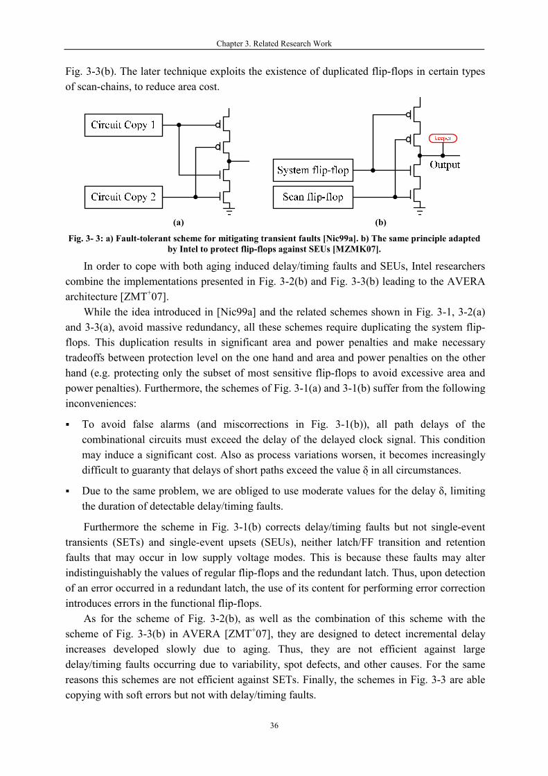
Chapter 3. Related Research Work
36
Fig. 3-3(b). The later technique exploits the existence of duplicated flip-flops in certain types of scan-chains, to reduce area cost.
(a) (b) Fig. 3- 3: a) Fault-tolerant scheme for mitigating transient faults [Nic99a]. b) The same principle adapted
by Intel to protect flip-flops against SEUs [MZMK07].
In order to cope with both aging induced delay/timing faults and SEUs, Intel researchers combine the implementations presented in Fig. 3-2(b) and Fig. 3-3(b) leading to the AVERA architecture [ZMT+07].
While the idea introduced in [Nic99a] and the related schemes shown in Fig. 3-1, 3-2(a) and 3-3(a), avoid massive redundancy, all these schemes require duplicating the system flip-flops. This duplication results in significant area and power penalties and make necessary tradeoffs between protection level on the one hand and area and power penalties on the other hand (e.g. protecting only the subset of most sensitive flip-flops to avoid excessive area and power penalties). Furthermore, the schemes of Fig. 3-1(a) and 3-1(b) suffer from the following inconveniences:
§ To avoid false alarms (and miscorrections in Fig. 3-1(b)), all path delays of the combinational circuits must exceed the delay of the delayed clock signal. This condition may induce a significant cost. Also as process variations worsen, it becomes increasingly difficult to guaranty that delays of short paths exceed the value δ in all circumstances.
§ Due to the same problem, we are obliged to use moderate values for the delay δ, limiting the duration of detectable delay/timing faults.
Furthermore the scheme in Fig. 3-1(b) corrects delay/timing faults but not single-event transients (SETs) and single-event upsets (SEUs), neither latch/FF transition and retention faults that may occur in low supply voltage modes. This is because these faults may alter indistinguishably the values of regular flip-flops and the redundant latch. Thus, upon detection of an error occurred in a redundant latch, the use of its content for performing error correction introduces errors in the functional flip-flops.
As for the scheme of Fig. 3-2(b), as well as the combination of this scheme with the scheme of Fig. 3-3(b) in AVERA [ZMT+07], they are designed to detect incremental delay increases developed slowly due to aging. Thus, they are not efficient against large delay/timing faults occurring due to variability, spot defects, and other causes. For the same reasons this schemes are not efficient against SETs. Finally, the schemes in Fig. 3-3 are able copying with soft errors but not with delay/timing faults.
Chapter 3. Related Research Work
37
3.2.2 Software-Based Soft-Error Mitigation Techniques Software-implemented hardware fault tolerance is a viable solution to the problem of developing processor-based systems that balance costs with dependability requirements. Since many different approaches are available, designers willing to adopt them may have difficulties in selecting the approach (or the approaches) that best fits with the design’s requirements.
As described above, when considering the possible effects of faults that can arise in a processor-based system, a common categorization distinguishes between faults who simply change the data of the application (thus forcing the code to produce wrong results, while following the same execution flow), and faults that affect the control flow, e.g., by changing the op-code of an instruction just before it is decoded and executed. Furthermore, when fault tolerance (and not only fault detection) capabilities are the target, the approaches presented (affecting data and control flow) are not enough. Some of them can be extended (at a higher cost in terms of memory, performance, and development cost) to cope with the more stringent requirements and new approaches can be devised to address these requirements. Consequently, in the following subsections we will present software-based soft-error mitigation techniques in three main categories: faults affecting the data, faults affecting the control flow and fault tolerance resorting only to changes in software.
3.2.2.1 Addressing Faults Affecting the Data The techniques for addressing faults affecting the data in the processor-based systems are generally rather expensive in terms of memory size, execution slow down and programming limitations. On the other side, they generally offer a very high coverage of the addressed faults. There are several well-documented techniques which deal with the faults affecting the data. 1). Computation duplication: The basic idea of this technique is that the operations performed by the code can be duplicated, and the produced results compared, thus allowing the detection of possible faults. Duplication may be implemented at four levels of granularity: instruction, instructions block, procedure, or program.
§ Instruction-level duplication: A simple method belonging to this category, and able to achieve a satisfactory error detection capability, has been originally proposed in [RRTV99a] it is based on introducing data and code redundancy according to a set of transformations to be performed on the high-level source code. The main advantage of the method lies in the fact that it can be automatically applied to a high-level source code [RRTV99b], thus freeing the programmer from the burden of guaranteeing its correctness and effectiveness (e.g., by selecting what to duplicate and where to insert the checks). The method is completely independent on the underlying hardware, and it possibly complements other already existing error detection mechanisms. On the other side, it also introduces a significant memory overhead (about 3 times with respect to the original program) and a comparable slow-down factor [CNV+00].

Chapter 3. Related Research Work
38
§ Procedure-level duplication: The selective procedure call duplication (SPCD) [OM02] technique is based on the duplication of the procedure execution. Every procedure (or a selected subset of them) is called twice with the same parameters; the results produced by the two executions are stored and compared, thus allowing the error detection. The main goal of this approach is the improvement of the system reliability by detecting transient errors in hardware, taking into account the reduction of the energy consumption and of the overhead. SPCD minimizes energy dissipation by reducing the number of clock cycles, cache accesses, and memory accesses by selectively duplicating procedure calls instead of duplicating every instruction. The obtained results show that SPCD allows an energy saving of 25% with respect to the energy consumption required by an instruction-level duplication approach [OSM02a].
§ Program-level duplication: Time redundancy is a typical technique that uses the program-level duplication. The same computation is performed multiple times (possibly in different forms) on the same hardware. A particular application of time redundancy is the duplication of the processing activity as a proper technique to detect faults of the underlying hardware. A particular form of such duplication is the virtual duplex system (VDS) architecture [Joc02]. The disadvantage of this time redundancy is the performance degradation caused by repetition of tasks. Simultaneous multithreading (SMT) [MKCG05] is a novel technique to improve the performance of a superscalar microprocessor. A SMT machine allows multiple independent threads to execute simultaneously, i.e., in the same cycle, in different functional units. VDS can be effectively exploited on a SMT machine, executing two threads in parallel, shifting time redundancy to spatial redundancy [RM00].
2). Executable Assertions: This method is based on the execution of additional statements that check the validity and correctness of the data corresponding to the program variables. The effectiveness of executable assertions method is highly application dependent. Moreover, in order to identify the most suitable executable assertions, the developers require extensive knowledge of the system. Error detection in the form of executable assertions can potentially detect any error in internal data caused by software faults or hardware faults. Executable Assertion and best effort recovery are proposed in [VAFK01], considering a control application.
3.2.2.2 Addressing Faults Affecting the Execution Flow Techniques aiming at detecting the effects of faults that modify the expected program’s execution flow are known as control flow checking (CFC) techniques. The basic idea of CFC is to partition the application program in basic blocks, i.e., branch-free parts of code. For each block a deterministic signature is computed and faults can be detected by comparing the run-time signature with a pre-computed one. In most control-flow checking techniques one of the main problems is to tune the test granularity that should be used.
Among the most important solutions based on the notion of basic blocks proposed in the literature.

Chapter 3. Related Research Work
39
Enhanced control flow checking using assertions (ECCA) is proposed in [ANKA99], it is able to detect all the single inter-block control flow errors (CFEs). However, it is neither able to detect intra-block control flow errors, nor faults that cause an incorrect decision on a conditional branch unit.
In paper [OSM02b], control flow checking by software signature (CFCSS) is presented. The disadvantage of CFCSS is that it cannot cover control flow error if multiple nodes share multiple nodes as their destination nodes.
Control-flow error detection through assertions (CEDA) method is proposed in [VA06]. Experimental analysis demonstrates that the achieved fault coverage is comparable with respect to that reached by other state-of-the-art approaches; with a lower performance overhead. The application of this technique reduces the ault coverage by a negligible value (i.e., from 99.3% to 99%), but the memory and performance overheads can be reduced by as much as 50%.
A software based technique for detection and correction of control flow errors called automatic correction of control flow errors (ACCE) [VGA07] is proposed. ACCE is an extension of the previous technique described in [VA06], which is able to detect inter-node control flow errors. It provides correct results in 90% of the test cases and imposes very low latency for error correction, with a performance overhead of about 20%.
Yet another control flow checking approach (YACCA) described in [GRRV03] demonstrates the effectiveness of the YACCA method as far as the fault coverage is considered. A very limited number of control-flow errors (CFEs) cause a failure, and the method shows itself to be more powerful than the considered alternative approaches.
3.2.2.3 Addressing Fault Tolerance When fault tolerance (and not only fault detection) capabilities are the target, the approaches presented so far are not enough. Some of them can be extended (at a higher cost in terms of memory, performance, and development cost) to cope with the more stringent requirements and new approaches can be devised to address these requirements. The techniques that are covered in this section are design diversity, checking-point, algorithm-based fault tolerance, and duplication.
§ Design diversity: Design diversity is the common technique adopted to achieve software fault tolerance. The two most common techniques implementing design diversity are N-version programming (NVP) [AA09] and recovery blocks (RB) [BD98]. These techniques have mainly been introduced to face the effects of software bugs. However, they can also be adopted to address hardware faults; they do not depend on any particular error model and are able to detect (and in some cases correct) both transient and permanent errors.
§ Checking-point: Checking-point is a commonly used technique for reducing the execution time for long-running programs in the presence of failures. With checking-point the status of the program under execution is saved intermittently in a reliable storage. Upon the occurrence of a failure, the program execution is restarted from the most recent checkpoint rather than from the beginning. Different recovery techniques can be used to

Chapter 3. Related Research Work
40
shorten the fault recovery time: rollback recovery [BMF06], stop and retry recovery [BMF06] and roll-forward checkpoint [PV94a] [GRL07]. In checking-point schemes a checking-point overhead is introduced due to the time duration required to store the processors’ states and the time to compare these states. The time spent for compare and store operations may vary significantly, depending on the system, and thus the checking-point overhead is determined mainly by the operation that takes a longer time.
§ Algorithm-based fault tolerance (ABFT): Hardening is obtained by adding coding information to matrices; however, while other approaches introduce coding information (to detect and possibly to correct errors) to each byte or word, these coding information are added to whole data structures (in this case to each matrix). The ABFT technique [TG00] [YOM01] is particularly attracting because it introduces a memory and performance overhead that, when compared with other techniques (e.g., TMR), is relatively limited. The method is able to detect and correct any error affecting a single element in the final matrix. On the other side, the correction capabilities are limited if an error affects more than one element in the resulting matrix. Moreover, this method is rather weak in detecting and correcting other kinds of faults, e.g., those affecting the memory elements in a microprocessor control unit.
3.2.3 Hybrid Soft-Error Mitigation Techniques Hybrid soft-error mitigation techniques combine hardware based techniques and SIFHT. They are effective since they provide a high level of dependability while minimizing the introduced overhead, both in terms of memory occupation and performance degradation. However, in order to be adopted, they mandate the availability of the source code of the application the processor core should run, and this requirement cannot be always fulfilled.
One such technique is described in [Ber06], and it combines the adoption of some SIHFT techniques in a minimal version (thus reducing their implementation cost) with the introduction of an I-IP in to the SoC. The software running on the processor core is modified so that it implements instruction duplication and information redundancy. Moreover, instructions are added to communicate to the I-IP the information about basic block execution. The module I-IP works concurrently with the main processor, it implements consistency checks among duplicated instructions, and it verifies whether the correct program’s execution flow is executed by monitoring the basic block execution.
In [Rho08], an approach aiming to minimize the overhead needed to harden a processor core has been proposed. The method is based on introducing in the SoC a further module (I-IP), whose architecture is general, that needs to be customized to the adopted processor core. The module I-IP monitors the buses of the processor. The results obtained by the processor and the module I-IP are then compared for correctness. Each time the processor fetches a new instruction, the module I-IP also checks the correctness of the address used by the processor by comparing it to the expected one. If a mismatch is found, which means an error is notified.
Another hybrid technique to mitigate single-event transients (SETs) in combinational logic based on duplication and time redundancy by using code word state preserving (CWSP) [Nic99a]. The CWSP stage replaces the last gates of the circuit by a particular gate topology

Chapter 3. Related Research Work
41
that is able to pass the correct value in the combinational logic in the presence of a transient fault. In the case of duplication, when the two copies of the inputs are identical (code word), the next state is equal to the corresponding output of the function. However, if the two copies of the inputs are not identical (non-code word), the next state remains equal to the present state. Using time redundancy, one of the inputs of the CWSP element is coming directly from the combinational circuit output, while the other input comes from the same output signal (this signal is delayed). The use of the method requires the modification of the CMOS logic in the next stage by inserting extra transistors and the necessity of using duplicated logic or logic to implement a delay. Furthermore, being also a time redundancy based technique, it will suffer from the same drawbacks already discussed in the subsection above as well.
3.3 Limitations of the Previous Works As soft errors become a stringent reliability issue in future nanometric technologies, design for soft-error mitigation is gaining importance. The objective of soft-error mitigation shifts from ensuring 100% soft-error tolerance regardless of cost to achieving an acceptable level of tolerance efficiency with reasonable overhead. According to the description in the previous sections, any fault tolerant approach, soft error mitigation may impact significantly area, speed and power; hence, the selection of the best approach is a complex trade-off between these parameters and the target level of reliability. It is therefore suitable to dispose a variety of solutions that can meet various constraints of the design, such as minimal area, minimum power, minimum speed, maximum reliability, or a trade-off between these parameters. We presented various schemes that exhibit such characteristics and could help the designer to meet product requirements. This section lists some limitations of the previous works introduced above from a high-level viewpoint.
1. Traditional soft-error mitigation techniques in mission-critical applications have been relying on costly redundancy-based approaches because cost has been of secondary concern. As soft errors become a reliability concern in cost-sensitive mainstream applications, existing techniques cannot be directly applied due to the tight design constraints and budget.
2. The majority of traditional soft-error mitigation techniques only target a kind of given fault model(s). However, due to the various types of process and environmental variations will add extra uncertainties to the power consumption, yield and reliability of the circuit, it is urgent and necessary to find a more efficient fault tolerant scheme to handle as many as potential fault models (SEUs, SETs, delay/timing faults, latch retention faults and clock skews, etc.).
3. Some of the soft-error mitigation techniques are not compatible or capable of being integrated with the standard cell-based ASIC design flow of exiting State-of-the-art electronic design automation (EDA) tools. This greatly reduces the possibility to integrate the mitigation techniques into most of the applications.

Chapter 3. Related Research Work
42
4. Traditional hardware based time redundancy techniques need to enforce stringent timing constraints during circuit synthesis process to guaranty that the minimum delay of any combinational block is larger than a certain duration δ. Such constraints are harder to meet under increasing parametric variations. Furthermore, in order to maintain the performance degradation at an acceptable level, the duration of δ has to be kept low, which will conversely affects the fault detection and/or correction efficiency of SETs and delay/timing faults.
5. Traditional software based soft-error mitigation techniques suffer from high detection latency in addition to the usual high performance and power overhead and complexity. Also, as to the threaded processors that achieve fault tolerance and recovery by executing two copies of the same program on a simultaneous multithreading processor, the selective insertion of duplicated instructions is quite difficult.
6. Some traditional hardware based soft-error mitigation techniques are applied only onto the critical paths or a certain functional unit of the targeted circuit to achieve area and/or power savings. These savings will also be accompanied with the increase of the yield and reliability.
3.4 Research Contributions Facing so many challenges stated above, it is imperative that revolutionary methodologies, techniques and flows need to be developed to facilitate the soft-error analysis and mitigation, as well as the design and optimization of nanometer circuits and/or systems with respect to power consumption, yield and reliability issues. This constitutes the primary objective of the research work presented in this dissertation.
The fault tolerant technique to be presented in this dissertation is applying double-sampling concept in latch-based designs to achieve high fault tolerance efficiency at low area and speed penalty. Due to these characteristics it represents a promising design paradigm for mitigating the flaws of CMOS nanometric technologies related to power dissipation, power density, yield and reliability. In addition, an integrated automation design framework of error detection architecture has been proposed, which integrates the synthesis process, error detection auto-loading algorithm, fault injection and functional fault checking together to facilitate and accelerate the design flow. We propose an error detection and correction scheme based on the described error detection architecture. However, this detection and correction architecture requires quite high area and power overhead as it uses redundant latches or flip-flop. Hence, we only implement GRAAL error detection architecture in this thesis. Lastly, a 32-bit low power latch-based processor is used as a case study to evaluate the cost overheads and fault detection efficiencies.
The advantages of the soft-error detection and/or correction architectures in this research work are:
1. Neither hardware duplication nor operation duplication is needed. Also, no hardened cell is needed;

Chapter 3. Related Research Work
43
2. The conflicting requirements of power consumption, yield and reliability are well-balanced;
3. Full circuit protection;
4. Target to almost all the relevant fault models (SEUs, SETs, delay/timing faults, latch retention faults, clock skews, etc) in deep nanometric technologies with respect to relative low power consumption, area, and speed penalty;
5. Large durations of delay/timing faults and transient faults are able to be detected and/or corrected;
6. No special timing constraints need to be employed during the synthesis process;
7. The whole design flow is capable of being integrated with the standard cell-based ASIC design flow of exiting state-of-the-art EDA tools;
In short, efficiency, overhead, scalability and integration are the key words that best describe the requirement for a promising power consumption, yield and reliability optimization solution. These aspects motivate all the research works presented in the following chapters.
3.5 Conclusion This chapter reviews various soft-error mitigation techniques at different abstraction levels: technology and device level, circuit level and architectural and system level. We present various schemes that exhibit such characteristics and could help the designer to meet product requirements. Active work in this area in various research centers should enrich the space of solutions and improve our ability to face the soft-error and other reliability threats that accompany nanometric scaling. Besides, the inconveniences of the previous works have also been addressed in order to highlight the main contributions in our research work. In the next chapter, we will introduce the mechanism of GRAAL fault tolerant architecture for mitigating the variability issues in nanometric technologies.

Chapter 3. Related Research Work
44

Chapter 4. GRAAL Fault Tolerant Design Paradigm
45
Chapter 4. GRAAL Fault Tolerant Design Paradigm
4.1 Latch-based Designs ............................................................................................ 46
4.1.1 Latch-based Design Principle ..................................................................... 46 4.1.2 Double-sampling Concept in Latch-based Design ..................................... 49
4.2 GRAAL Error Detection Architecture ................................................................ 51 4.2.1 Error Detection Mechanism ........................................................................ 51 4.2.2 Error Detection Efficiency Analysis ........................................................... 54
4.3 GRAAL Error Detection and Correction Architecture ........................................ 57 4.4 Employing GRAAL to Improve Yield, Reliability and Power Dissipation ........ 59 4.5 Conclusion ........................................................................................................... 60
s presented in chapter 3, the fault tolerant techniques for mitigating logic
soft errors at different abstraction levels all have their own drawbacks.
Clearly, the requirements for high yield, high reliability and low power dissipation are
contradictory. The goal of this chapter is to propose an approach that conciliates the
above contradictory requirements and provide a global solution called GRAAL
(Global Reliability Architecture Approach for Logic) to the yield, reliability and
power dissipation issues in nanometric technologies. GRAAL architecture is presented
to meet the requirements mentioned above, which applies double sampling concept in
latch-based designs to achieve high fault tolerant efficiency. It targets more kinds of
the fault models, such as single-event upsets (SEUs), single-event transients (SETs),
delay/timing faults, latch retention faults as well as clock skews with relatively lower
area overhead, power dissipation and speed penalty.
A

Chapter 4. GRAAL Fault Tolerant Design Paradigm
46
4.1 Latch-based Designs The basic idea of GRAAL fault tolerant architecture is applying double-sampling concept in latch-based designs to achieve high fault tolerant efficiency with relatively lower area, power dissipation and speed penalty. Previous schemes using double-sampling in traditional flip-flop based designs have many inconveniences. For instance, checking the results of a single computation at two different instants leaves a low time budget for detecting timing and transient faults and imposes undesirable timing constraints during the synthesis process.
By combining double-sampling concept with the latch-based design style, GRAAL fault tolerant architecture eliminates the drawbacks in previous works and also enables detecting and correcting delay faults (timing faults) and transient faults with much higher duration, as well as SEUs and latch faults. As expected, GRAAL fault tolerant architecture does not use hardware replication and also it neither uses computation replication, which is different with the traditional double-sampling concept in flip-flop based designs. Instead, it performs error detection by observing the output signals of a single computation at two different instants with a large time interval.
4.1.1 Latch-based Design Principle The synchronization and state storage in a sequential design is typically implemented with one of the two devices: edge-triggered flip-flops or level-sensitive latches. However, latches are not traditionally used in ASIC designs, despite it being possible to specify latches at register transfer level (RTL). Many designers are less familiar with latch-based design methodology, and it is easier to ensure correct timing behavior in flip-flop based designs. Latch-based designs are gaining popularity in the state-of-the-art high performance synchronous circuit design due to their smaller size, lower power consumption, and faster operation speeds. In [CNK01], a latch-based design is recommended for ASIC since timing could be improved 25% just by using latches instead of flip-flops. Thus, latch-based designs are more commonly used in custom designs, but recently, they have been identified as a design approach to increase the speed of ASICs.
Latch is a level-sensitive element with following functional behaviour: when the control signal (clock) is at the active level, the latch is transparent, i.e. the output follows any transition at the input; when the clock is at the inactive level, and the latch is opaque, i.e. it holds the state. The transition of the clock signal from the active level to the inactive level is referred to as the latching edge, since the state of the output cannot be changed after this edge. Similarly, we define the releasing edge of the clock as the transition of the clock signal from the inactive level to the active level. Depending on the values of the active and inactive level of the control signal, a latch can be high-level transparent (when active level is logical high) or low-level transparent (when active level is logical low).
The notable advantage with latch-based design is the time borrowing. It allows a natural repartition of computation time when using pipeline structures. Fig. 4-1 shows a design using a simple two-phase clock scheme. Let L1, L2, L3 and L4 be storage elements, and C1, C2, C3 and C4 be combinational circuits, respectively. For designs using edge-triggered flip-flops,

Chapter 4. GRAAL Fault Tolerant Design Paradigm
47
the clock period has to be at least 8ns because the longest path in any combinational circuit is 8ns. But, if the design uses latches and is driven by a two-phase clock as shown in the figure, since the 8ns is within the enabled period of L2, the signal along the path1 can pass through L2 and continue on the path2. Since the delay along the path2 is 2ns, which is short enough to compensate for the overdue delay of path1, this design will work properly. For the same reason, path3 can borrow some time from path4 without any timing violation. A latch-based design completes the execution of the four logic stages in 20ns, whereas an edge-triggered based design needs 32ns (4 x 8ns).
path2
Fig. 4- 1 Time borrowing example for a latch-based pipeline design
With latches, the slowest pipeline stage can borrow time from either or both the previous and next pipeline stage. This gives designers a lot of flexibility in designing circuits, especially high performance custom design. As a result, the delay of a combinational logic path of a design using edge-triggered flip-flops cannot be longer than the clock period except for those specified as false paths and multiple-cycle paths. The performance of a circuit is therefore limited by the longest path of a design. With more and more designs pushing for higher performance, more and more designers are turning into latch-based design methodology because it allows the use of longer combinational path delays as long as it can be compensated by shorter path delays in the subsequent logic stages.
Another interesting property of a latch-based design is that, level-sensitive latches are less subject to setup time and clock skew. In fact, there are multiple reasons which lead to clock skews in the design. The variation of the supply voltage, more than one clock, unbalanced delays in the clock tree, and process variation and temperature variation during operation all might incur clock skews. With latch-based design, the clock skew becomes relevant only when its value is close to the non-overlapping duration of the clocks (half the period of the master clock). When working at lower frequency which increasing the non-overlapping of clocks, the clock skew is never a problem, and can be even safely ignored. This superiority in latch-based design allows the designer to perform synthesis and routing by

Chapter 4. GRAAL Fault Tolerant Design Paradigm
48
using smaller clock buffers thus simplifying the clock tree generation, which will reduce the power consumption of the clock tree and also lighten the clock skew timing constraints.
However, latch-based designs have also some drawbacks. Commercial synthesis and place-and-route tools provide only limited support for latch-based designs. Besides, it is also more difficult to conduct timing analysis and verification in latch-based designs. However, normal alternative approaches such as gate-level simulation can be used for the verification for latch-based designs.
4.1.1.1 Timing Analysis in Latch-based Design As explained in the previous section, the timing analysis in latch-based designs is much more complicated than flip-flop based designs. Hence, in this section we illustrate the operation of an example latch-based linear pipeline.
A simplified latch-based high-speed pipeline can be modeled as shown in Fig. 4-2. In Fig. 4-2, Ci and Lj represent combinational logic blocks and latches respectively. Every latch is assumed to be a positive D-latch, which means that the latches become transparent when the corresponding clock is high. Even though the figure shows complementary clocks for simplicity, any type of clocks can be used, including two-phase non-overlapping, four-phase non-overlapping, or four-phase overlapping [CNK01]. To simplify the discussion, all latches are assumed to be ideal latches where all delays as well as the setup time and hold time are all zero.
Fig. 4- 2 Timing analysis on an example latch-based design rated by two complementary clocks
Assume C1 is the first combinational logic block of the high-speed pipeline. We consider the inputs to the latches driving C1 as primary inputs, and assume that a new combination of values is applied at the inputs of block C1 at the rising edge of the driving clock Φ1 that occurs at t1. The values at the outputs of C1 must stabilize some time before the subsequent falling edge of the block’s receiving clock, i.e. the clock controlling the latches at its outputs,
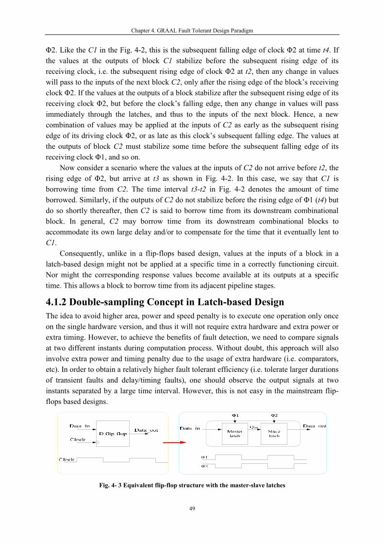
Chapter 4. GRAAL Fault Tolerant Design Paradigm
49
Φ2. Like the C1 in the Fig. 4-2, this is the subsequent falling edge of clock Φ2 at time t4. If the values at the outputs of block C1 stabilize before the subsequent rising edge of its receiving clock, i.e. the subsequent rising edge of clock Φ2 at t2, then any change in values will pass to the inputs of the next block C2, only after the rising edge of the block’s receiving clock Φ2. If the values at the outputs of a block stabilize after the subsequent rising edge of its receiving clock Φ2, but before the clock’s falling edge, then any change in values will pass immediately through the latches, and thus to the inputs of the next block. Hence, a new combination of values may be applied at the inputs of C2 as early as the subsequent rising edge of its driving clock Φ2, or as late as this clock’s subsequent falling edge. The values at the outputs of block C2 must stabilize some time before the subsequent falling edge of its receiving clock Φ1, and so on.
Now consider a scenario where the values at the inputs of C2 do not arrive before t2, the rising edge of Φ2, but arrive at t3 as shown in Fig. 4-2. In this case, we say that C1 is borrowing time from C2. The time interval t3-t2 in Fig. 4-2 denotes the amount of time borrowed. Similarly, if the outputs of C2 do not stabilize before the rising edge of Φ1 (t4) but do so shortly thereafter, then C2 is said to borrow time from its downstream combinational block. In general, C2 may borrow time from its downstream combinational blocks to accommodate its own large delay and/or to compensate for the time that it eventually lent to C1.
Consequently, unlike in a flip-flops based design, values at the inputs of a block in a latch-based design might not be applied at a specific time in a correctly functioning circuit. Nor might the corresponding response values become available at its outputs at a specific time. This allows a block to borrow time from its adjacent pipeline stages.
4.1.2 Double-sampling Concept in Latch-based Design The idea to avoid higher area, power and speed penalty is to execute one operation only once on the single hardware version, and thus it will not require extra hardware and extra power or extra timing. However, to achieve the benefits of fault detection, we need to compare signals at two different instants during computation process. Without doubt, this approach will also involve extra power and timing penalty due to the usage of extra hardware (i.e. comparators, etc). In order to obtain a relatively higher fault tolerant efficiency (i.e. tolerate larger durations of transient faults and delay/timing faults), one should observe the output signals at two instants separated by a large time interval. However, this is not easy in the mainstream flip-flops based designs.
Fig. 4- 3 Equivalent flip-flop structure with the master-slave latches

Chapter 4. GRAAL Fault Tolerant Design Paradigm
50
Most common implementation of flip-flop consists of two cascaded identical latches transparent on opposite levels of the input clocks (complementary clock phases). In this way, a master-slave latch pair behaves as an edge-triggered storage element, which is shown in Fig. 4-3.
Fig. 4-4 illustrates an example pipeline stage of a flip-flops based design. In the circuit, there are two combinational blocks called CC1 and CC2 and also with two flip-flops, each of the flip-flops is composed by master and slave latches.
Fig. 4- 4 Flip-flop based design style with complementary clock phases
We can observe that, at the rising edge of the clock Φ1, the outputs of CC1 and CC2 are captured by the master latches and new inputs are applied on combinational blocks CC1 and CC2. Thus, after the rising edge of the clock, the values of the new inputs begin to propagate through CC1 and CC2. Consequently, the outputs of CC1 and CC2 remain stable for very short intervals (equal to the minimum delays of CC1 and CC2). During synthesis process, by setting the timing constraints on CC1 and CC2 to guaranty that their shortest paths have delays larger than a certain value δ, we can ensure that the outputs of CC1 and CC2 will remain stable for a duration larger than δ [Nic99a] [Ern03b]. However, the value δ cannot be large due to the fact that it will induce higher area, power and speed overhead. Also as path delays can be affected by process parameter variations, the minimum delays of the shortest paths under process parameter variations have to be taken account of the erroneous circuit behavior, which further reduce the value δ. In summary, with a flip-flops based design style, it is complicated to set the value δ and also to observe the output signals at two instants separated by a relatively large time interval.
An alternative way for solving this problem is by using different time intervals to perform computation at adjacent pipeline stages. Hence, when one stage is computing, its adjacent stage is idle and the outputs are stable, which can be used for temporary faults checking. This is not the case in flip-flops based designs like adjacent stages such as CC1 and CC2 in Fig. 4-4 performing computation simultaneously. However, a more thorough insight into the pipeline illustrated in Fig. 4-4 can show that, the master and slave latches are rated by the complementary clock phase and thus they perform computation at different time intervals. Then we can exploit this fact by modifying the circuit in Fig. 4-4 to achieve our goal. Thus, if we transform a flip-flop based design (in Fig. 4-4), into its equivalent latch-based design, by moving the slave latches from the outputs of the master latches in the middle of the

Chapter 4. GRAAL Fault Tolerant Design Paradigm
51
combinational circuits as shown in Fig. 4-5, we obtain a design that can function at the same clock frequency as the original one.
Fig. 4- 5 Pipeline stages in latch-based design with non-overlapping clock phases
In addition, as seen above, the master and slave latches operate at different clock phases. This implies that in the modified design the output signals of any combinational block (inputs of the latches), remain stable during the period in which its adjacent blocks are in computation. Thus, we can compare the outputs of the latches against their inputs to detect delay/timing faults of large duration. In order to maximize the time intervals during which the signals of each pipeline stage maintain the stable values. The clocks should be scheduled by using two non-overlapping clocks Φ1 and Φ2. We observe that the search for an ideal fault tolerant architecture leads to the well known latch-based design style by using non-overlapping clocks.
Next section, we will exploit the above observations to provide cost-efficient error detection architecture based on double-sampling concept in latch-based design style.
4.2 GRAAL Error Detection Architecture GRAAL error detection architecture described in [Nic07] is based on the observation that, in latch-based designs, when one pipeline stage is computing, its adjacent stages are in stable state and vice-versa. Thus, latch-based designs with non-overlapping clocks offer comfortable periods of signal stability (the stable state period of the stage producing them) during which they can be checked. This can be done by comparing the inputs against the outputs of the latches of each stage during its stable state period. GRAAL architecture has two variants, an error detection version, and an error detection and correction version. In this section, we will explain GRAAL error detection architecture in details and then analyze the soft-error detection efficiency.
4.2.1 Error Detection Mechanism A latch-based design pipeline stage similar to Fig. 4-5 and shown in Fig. 4-6, uses transparent latches instead of flip-flops. To avoid the case where subsequent latch stages are simultaneous in the transparent state, subsequent latch stages are rated by two non-overlapping clocks, Φ1 and Φ2. The latches are transparent on the high level of their associated clock and allow time borrowing, which is often used to trade detection capabilities with speed.

Chapter 4. GRAAL Fault Tolerant Design Paradigm
52
Fig. 4- 6 Latch-based design style and its rated clocks
In the following, similar to [AMP00], the duration of the high level of each of the clocks Φ1 and Φ2 is T/4 (where T is the clock period of the initial flip-flop based design). This leaves another T/4 of non-overlapping period between the high levels of the two clocks. The idea is to exploit inherent properties of this design style highlighted above, to optimize fault tolerance efficiency. The latches in odd pipeline stages (L1, L3 …) are clocked by the clock Φ1 and will be transparent during the high level of Φ1. The latches in even pipeline stages (L2, L4 …) are clocked by the clock Φ2 and will be transparent during the high level of Φ2. The combinational logic blocks (CC1, CC2 …) have delays that do not exceed the half period of the clock cycle (T/2), except in case where time borrowing is used to increase speed. For simplicity, considering the case where the delays of the circuit are evenly distributed along the different pipeline stages, the maximum delay of each stage will not exceed T/2. Thus, the time during which odd stages perform computations can be situated from the middle of the ‘1’ level of Φ2 to the middle of the ‘1’ level of Φ1, while even stages can perform computations from the middle of the ‘1’ level of Φ1 to the middle of the ‘1’ level of Φ2. Time borrowing is possible in some situations. For instance, if the delay of a stage (say stage CC3) is larger than T/2, and the delay of its subsequent stage (let’s say stage CC4) is less than T/2, then, the computation in the CC3 stage will finish later than expected and will leave less time for computation to the next stage (CC4). However, the computation of the two stages can be completed in time, as CC4 can complete its computation in a time shorter than T/2.
We can have the following observations from the discussion above:
1). The falling edge of Φ1 occurs after the output signals of odd combinational logic (CC1, CC3 …) reach their steady state. The delay between this instant and the falling edge of Φ1 is referred as D (see Fig. 4-7).
2). The latches of even stages (L2, L4 …) are blocked (their outputs are stable) during the low level of Φ2.
3). The point 2) guaranties that the inputs of odd combinational blocks (CC1, CC3 …) are stable until the rising edge of Φ2. Thus, the outputs of each of these blocks (inputs of L1, L3 …) are stable at least until the rising edge of Φ2. In fact, they will be stable even after this instant and for a time duration equal to the minimum delay δ (see Fig. 4-7) of each

Chapter 4. GRAAL Fault Tolerant Design Paradigm
53
odd combinational block. A similar situation holds true for the stability of the outputs of even combinational blocks (inputs of L2, L4 …).
Fig. 4-7 shows GRAAL error detection architecture. According to the points 1), 2) and 3) described above, we can compare the outputs of odd latches L1, L3 … against their inputs (i.e. the outputs of odd combinational blocks CC1, CC3 …) at any time during their stability period. Also from points 1), 2) and 3), the duration of the stability period (shown in Fig. 4-7 as a hashed area), is D+T/4+δ. Thus, the faults modifying the equality between the inputs and the outputs of L1, L3 … during this period can be detected. The similar principle can be used for even stages. These observations lead to a low-cost error detection scheme, consisting in comparing the inputs of the latches against their outputs and detecting SEUs, SETs and delay/timing faults of large duration. This is illustrated in Fig. 4-7, where a two-input XOR gate compares the input of each latch with its output. In addition, pipelined OR trees will be used to group the outputs of the XOR gates into error detection signals (this mainly depends on the number of clock domains in the design). Finally, the flip-flops are used to synchronize and capture the error signals. For instance, the error signals generated in the odd stages are synchronized and captured using the rising edge of Φ2 (driven clock of even stages); the error signals generated in the even stages are captured using the rising edge of Φ1 (driven clock of odd stages).
Fig. 4- 7 GRAAL error detection architecture
However, the soft-error may affect several neighborhood cells at the same time, leading to multiple cell upsets (MCUs) [MHZA03] [JOO+99]. Thus, several bits will be affected by the same event. This is an increasingly critical problem for latest technological processes

Chapter 4. GRAAL Fault Tolerant Design Paradigm
54
(such as 45nm and 32nm). The schemes in [Ern03b] [Nic07] are vulnerable to this phenomena, as errors could affect both the functional flip-flop and the associated redundant latch. This is not the case for the scheme of Fig. 4-7, where no redundant latch is used, making the scheme insensitive to MCUs.
A problem related with the scheme of Fig. 4-7, is the metastability in the error generation path. Metastability can lead to undetected errors since metastable values could be interpreted differently by the next pipe-line stage and by the error detection circuitry. Thus, it may reduce the mean-time to undetected failures. According to the target mean-time to undetected failure requirement, metastability detectors, as the ones described in [Ern03b], might be required.
Last but not least, thanks to the long duration of signal stability in latch-based designs, error detection in Fig. 4-7 does not duplicate the system latches. Only comparators are added. As a matter of fact, the scheme of Fig. 4-7 is expected to induce much lower area and power penalties with respect to the schemes of Fig. 3-1, 3-2 and 3-3 in chapter 3.
4.2.2 Error Detection Efficiency Analysis Similarly to the previous scheme in [Ern03b] [Nic07], faults affecting the latches/flip-flops (SEUs and latch retention faults) will be detected by the comparison. Consequently, for the errors which affect the latch (SEUs and latch retention faults) will be easily detected using GRAAL error detection architecture. In this sub-section, we will mainly focus on the other fault models, such as single-event transient faults (SETs), delay/timing faults and clock skews.
4.2.2.1 Single-event Transient Faults (SETs) Concerning single-event transient faults, enabling the comparison at the end of the D+T/4+δ period maximizes the duration of detectable SETs. However, this will introduce short-path constraints in the synthesis process, similar to the ones encountered with the schemes in [Ern03b] [Nic07]. Enforcing such constraints becomes increasingly complicated due to the increasing variations in upcoming process nodes. Thus, we disregard δ in the above formula and we consider that the comparisons in odd latches are performed at the rising edge of Φ2 and in even latches at the rising edge of Φ1. In this way we simplify the synthesis process and make the implementation simpler and more robust, while still allows detecting large temporal faults (i.e. all single-event transient faults of duration up to D+T/4. The value of D depends on how delays are distributed among consecutive pipeline stages). If delays are evenly distributed and the data at the output of odd/even latches are ready in the middle of the high level of Φ1/Φ2, then, D will be T/8. So the detectable duration of single-event transient faults will be around 3T/8. The situation where delays are evenly distributed among pipeline stages is ideal. In practice, the max delays in some stages exceed T/2 and the max delays in some other stages are less than T/2. This situation happens when time borrowing is used to increase speed. In this case, the duration of detectable delay/timing faults in some stages will be larger than 3T/8 and in some other stages lower than 3T/8, but still larger than T/4. If we do not disregard δ (where δ is the minimum delay of the checked combinational logic block), we achieve much higher error detection efficiency. This result is valid if we check the signals of odd/even stages at time duration δ after the rising edge of Φ2 or Φ1.

Chapter 4. GRAAL Fault Tolerant Design Paradigm
55
4.2.2.2 Delay/timing Faults Considering that the delay of each latch-based pipeline stage will be roughly the half of the flip-flop based pipeline stage, the delays of each latch-based pipeline stage will not exceed a half of the clock period, T/2 (considering the same clock period for the flip-flop based and the latch-based case). In this case, the outputs of each pipeline stage will be ready at the rising edge of the corresponding clock. Based on these assumptions, and using a more accurate estimation than in [Nic07], we can show that the scheme of Fig. 4-7 detects delay/timing faults of duration up to 100% of the critical path delays (T/2), without imposing any constraint on short paths. Thus, it offers very comfortable timing margins that can be employed for detecting large delay/timing faults induced by spot defects, variability and circuit aging by the reduction of VDD in case we use power reduction techniques [Das05]. If we add short path constraints the detectable delay/timing faults are further increased.
However, previously in the evaluation of error detection efficiency of the single-event transient faults and delay/timing faults, we disregarded δ timing constraints, as the detecting faults of duration around D + T/4 is largely sufficient. Moreover, this removes the stringent timing constraints required during the synthesis of the scheme in Fig. 3-1, 3-2 presented in chapter 3 as well as the related risk of erratic behavior due to process parameter variations. Such variations could result some paths in a relatively lower value of δ, which will lead to systematic false alarms.
4.2.2.3 Clock Skews In addition to the transient faults and delay/timing faults, a significant duration of clock skews induced by the variation of the supply voltage and PLL noise and also by the process parameter variations or unbalanced clock tree delays can be tolerated or detected by GRAAL error detection architecture.
1). Clock skews tolerance As described in the previous section, the analysis of clock skews depends on how delays
are distributed among consecutive pipeline stages. For simplicity we assume the typical case where the pipeline stages have delay durations equal to T/2. This means that the analysis will be pessimistic for the majority of stages but optimistic for some of them.
In the typical case, the data at the output of odd latches are stable in the middle of the high level of clock Φ1 and the data at the output of even latches are stable in the middle of the high level of clock Φ2. Consider that the high phase of Φ2 is skewed and occurs earlier than expected (up to T/8 of the clock period). This case is shown in Fig. 4-8 (positive skew on Φ2). In this case, the falling edge of the skewed clock Φ2 coincides with the middle of the non-skewed Φ2. At this moment the data are stable and the outputs of the even combinational blocks are captured by the downstream even latches. The period between the captured moment and the middle of the high phase of clock Φ1, the odd stages perform their computations as expected. Suppose now that the high phase of Φ2 is skewed and occurs later than expected (up to T/8 of the clock period), which is shown at the bottom of Fig. 4-8 (negative skew on Φ2). In this case, the rising edge of the skewed clock Φ2 coincides with the

Chapter 4. GRAAL Fault Tolerant Design Paradigm
56
middle of the non-skewed clock Φ2. At this moment the data are stable and the outputs of the even combinational blocks are captured by the downstream even latches. The period between the captured moment and the middle of the high phase of clock Φ1, the odd stages perform their computations as expected. The skews occur on clock Φ1 is the similar case with clock Φ2. Consequently, clock skews of T/8 of the clock period will be tolerated.
Fig. 4- 8 Clock skews tolerance and/or detection
2). Clock skews detection § Suppose the case where the high phase of clock Φ2 occurs earlier than T/8 of the clock
period. In this case, data captured by even latches may be erroneous. According to the error detection scheme mentioned above, the outputs of even latches should be compared against the outputs of even combinational blocks (correct data) at the rising edge of clock Φ1. The comparison between the two values will not be equal, thus the clock skew that occurs on clock Φ2 is detected.
§ Suppose another case where the high phase of clock Φ2 occurs later than T/8 of the clock period (in this case, data will be captured after the middle of the high phase of non-skewed clock Φ2 by the even latches). However, this will leave less time for the computations in the next pipeline stage (i.e. CC3). The data are captured by the latch L3 in this stage might have two possibilities:
a) Erroneous data are captured by latch L3 at the falling edge of clock Φ1. In this case, it is easy to check the comparator in this stage to flag an error.
b) Correct data are captured by latch L3 at the falling edge of clock Φ1. In this case, these correct data are supposed to be stable before the middle of the high level of clock Φ1. If these data are stable after the middle of the high level of clock Φ1, the computation time in the next pipeline stage will be largely reduced and so on. In the end, there must exists a latch in the downstream pipeline stage that capture erroneous data, thus the corresponding error signal will be detected. In summary, skew occurs later than 12.5% of clock period on the clock signal can be detected as well.
Chapter 4. GRAAL Fault Tolerant Design Paradigm
57
3). Skews on the clock signal validating the error signals According to the error detection mechanism discussed above, we need to check the error
signals by using the rising edge of the corresponding clock signals. For instance, the validations of the error signals in even stages should be conducted at the rising edge of clock Φ1. This can be done by using directly Φ1 or by introducing a delay on this clock signal to account for the delay of the comparator (comp.2). If there is a negative skew with duration of more than the shortest delay of combinational blocks CC2, then, using this skewed clock signal to validate the error2 signal will lead to an erroneous detection due to the fact that the outputs of CC2 can change before the clocking edge of the validation clock. Obviously, no erroneous detection occurs if the validation edge occurs earlier than expected. The consequence is a reduction of the time interval available to check stage CC2, leading to a reduction of the duration of detectable transient faults and/or delay/timing faults.
In summary, the properties described above make the proposed architecture very robust to clock skews, in complex SoCs composed of several tens or hundreds of processing nodes, global clock skews may become larger than the tolerant skew duration), thus inducing frequent error detections. For such complex designs the proposed scheme may have to be combined with a GALS approach (Globally Asynchronous, Locally Synchronous architecture) [MHK+99].
4.3 GRAAL Error Detection and Correction Architecture Error detection may be sufficient in many applications. For instance, in cryptographic circuits it may be sufficient to detect a fault attack and block the circuit to prevent retrieving cryptographic information. In other applications system error recovery may be required. It can be based on a simple reboot if loosing the application context is acceptable, or on more complex schemes like check-point and rollback recovery. In both cases, repeated error detection can be monitored and operation frequency can be lowered and/or voltage level increased to eliminate eventual delay/timing faults or latch retention faults that lead to frequent interruptions with long error recovery time. But in other applications fast error recovery could be required. In these cases the fault-tolerant architecture must include mechanisms able to perform fast error correction. One possibility is to rethink the processor architecture to support fine-grain error recovery: activate a pipeline flush and restart the execution of all instructions that were not completed at the cycle of error detection. Another possibility is to use redundant latches or flip-flops to perform local error recovery.
GRAAL fault tolerant architecture has two variants: one is based on error detection only; another one includes also the correction architecture. Fig. 4-9 illustrates the error detection and correction scheme related to GRAAL approach. In this scheme the use of redundant data flip-flops allows the highest error detection and recovery efficiency. If a lower efficiency is required, redundant latches instead of flip-flops can be used. In this work, we use redundant flip-flops to implement the error recovery mechanism.

Chapter 4. GRAAL Fault Tolerant Design Paradigm
58
Fig. 4- 9 GRAAL error detection and correction architecture
In Fig. 4-9, the outputs of CC1/CC2 are memorized by latch L1/L2 at the falling edge of clock Φ1/Φ2. The same data are memorized by the redundant DFF1/DFF2. If we do not use minimum path constraints of combinational blocks during the synthesis process, then we will activate this memorization at the next rising edge of Φ2/Φ1, as indicated in Fig. 4-9. We can also impose the constraint that delay of minimum paths exceeds T/4 during synthesis process. In this case, we will activate this memorization at the next falling edge of Φ2/Φ1. In the following we consider the former case (redundant DFF1/DFF2 capture their inputs at the rising edge of Φ2/Φ1). As highlighted in the previous section, in latch-based designs we can use the data of only even stages or of only odd stages to restore the data of all stages. This is exploited in Fig. 4-9 to achieve efficient error recovery. The error signals error1 and error2 are crossed to control the 2-to-1 multiplexers, that is, the 2-to-1 multiplexers of odd (even) stages are controlled by the error signal of even (odd) stages (error2/error1). These signals are all 0 in fault-free operation and the outputs of combinational circuits are connected to the inputs of corresponding latches. For simplicity, in case of error detection in an odd stage (for instance, transient fault or timing fault in CC1, or SEU in L1), error recovery is performed according to the following steps:
1). The activation of the error signal error1 prevents the regular latch L2 to capture the output data of combinational circuit CC2 at the falling edge of Φ2, and also the redundant DFF2 remains original data before the next rising edge Φ1 (hold signal of redundant DFF2 activated or high level of Φ1 is frozen). The time duration between the rising edge of Φ2 that captures data in DFF1 and the next rising edge of Φ1 that captures data in DFF2 (half clock period) is available for performing the comparisons and blocking the redundant DFF2 (freeze their clock signals to 0). This is equal to the time available each pipeline stage for performing its computation.
2). The error signal error1 controls the MUX2 to transfer the contents (original value) of redundant DFF2 to latch L2. At the falling edge of Φ2 that follows the frozen phase of Φ1 these data are memorized by the latch L2. The combinational circuits CC1 receive these data to perform computation.

Chapter 4. GRAAL Fault Tolerant Design Paradigm
59
3). The results of the computation of combinational circuits CC1 are captured by the latch L1 at the subsequent falling edge of Φ1. At this instant the contents of all regular latches (L1 and L2) are restored to the correct values that they were expected to have at the clock cycle during which the error occurred. Since error detection in an odd (even) stage uses the data of even (odd) stages for error recovery, this scheme tolerates not only the delay/timing faults but also transition faults as well as the SEUs and other flip-flop and latch faults. The case while an error detected in an even stage is similar with the discussion above.
Under the condition that the half clock cycle is sufficient to compute the odd (even) error the state of the even (odd) flip-flops is frozen during this time interval, as described above, all detectable errors are correctable since no erroneous data are used for performing it. As concerning error detection, a similar analysis as for Fig. 4-7 shows that the architecture of Fig. 4-9 has the same detection capabilities as Fig. 4-7 with respect to delay/timing faults, SETs, SEUs and weak latch and flip-flop faults. The situation is also similar to figure 8 for clock skews, with the following difference: the results on clock skews concerning the clock signals used to validate the error signals of even and odd stages in the scheme of Fig. 4-7 apply to the clock skews concerning the clock signals used to control the flip-flops of even and odd stages in Fig. 4-9.
The error correction can be global, that is, the error signals of all odd/even stages are compacted into a global odd error signal ERR1/ERR2. When the ERR1/ERR2 signal is activated the 2-to-1 multiplexers of all even/odd stages are controlled to use the content of the flip-flops of all even/odd stages to re-compute the state of the whole circuit. If the time available for computing the ERR1/ERR2 signal and blocking the odd/even flip-flops of the full circuit (half of the clock period) is not sufficient for performing these actions, error correction can be performed locally (re-compute the state of the pipeline stage affected by the error by means of the contents of the flip-flops of the previous pipeline state). Then, the state of the full circuit can be restored by using counter-flow pipelining techniques like in RAZOR [Ern03b]. This kind of technique is applicable on processor architectures. For portions of logic in a SoC, which are not part of processor cores, the global error correction scheme can be used as far as these portions are not very large to accommodate the computation of the ERR1/ERR2 signals and freeze the clock of even/odd flip-flops within a half clock period.
Note finally that in Fig. 4-9 the 2-to-1 multiplexers are schematically inserted between the combinational circuits and the latches. However, in order to avoid adding the multiplexer delay in the signal paths, in practice, the 2-to-1 multiplexers will be inserted in the feedback loop of the latches.
4.4 Employing GRAAL to Improve Yield, Reliability and Power Dissipation The capabilities of the new architectures for detecting and/or correcting delay/timing faults and weak-latch/flip-flop faults can be exploited to improve yield and reliability in nanometric technologies, as the vast majority of faults affecting them can be detected and/or corrected by

Chapter 4. GRAAL Fault Tolerant Design Paradigm
60
the GRAAL architectures. These capabilities can also be exploited to reduce power dissipation. The idea for reducing power dissipation is that when reduce the voltage level inherent, and weak latch or flip-flop faults may appear. Because the proposed architectures can detect delay/timing faults of higher duration than other fault tolerant techniques, we have comfortable margins to allocate a part of to reduce the voltage level and another part of this duration to tolerate faults affecting yield and reliability. Furthermore, the ability of the new architectures to tolerate clock skews should enable further power reduction by relaxing the clock trees construct, which are known to consume significant amounts of the power dissipated by modern ICs.
4.5 Conclusion This chapter proposes GRAAL fault tolerant architecture for mitigating the flaws of very deep nanometric technologies scaling. GRAAL fault tolerant architecture has two variants, error detection architecture and error detection/correction architecture. Each of them applies double-sampling concept in latch-based designs to achieve high fault tolerant efficiency at lower area, power and speed penalty. Also, this fault tolerant architecture is able to handle almost all types of the temporary faults such as SEUs, SETs, delay/timing faults, latch retention faults as well as clock skews.
Besides, this chapter briefly describes the issues related to yield, reliability and power dissipation with GRAAL fault tolerant architecture. Full error detection architecture and/or full error detection/correction architecture are necessary for achieving a maximum improvement of yield and reliability in deep nanometric technologies scaling. We believe that error recovery (correction) architectures at higher level, like instruction-level rollback (retry), are more area and power efficient.

Chapter 5. Integrated Framework for GRAAL Fault Detection Architecture
61
Chapter 5. Integrated Framework for GRAAL Fault Detection Architecture
5.1 Integrated Automatic Design Framework Overview ........................................... 62 5.2 Synthesis Process ................................................................................................. 63 5.3 GRAAL Circuit Hardening Process .................................................................... 64 5.4 Fault Injection System ......................................................................................... 65
5.4.1 Fault Injection Techniques Overview ......................................................... 65 5.4.2 Fault Injection Mechanism ......................................................................... 67
5.5 Results Analysis Platform ................................................................................... 75 5.5.1 Functional Failure Checking ...................................................................... 77 5.5.2 Fault Classifications ................................................................................... 77
5.6 Conclusion ........................................................................................................... 78
ue to complexity of the processor-based system, it is not feasible to
implement and validate GRAAL fault detection technique manually. A
reasonable idea is to provide an integrated automatic design framework, which helps
automating and accelerating the entire design and verification flow. This chapter
presents an integrated automatic design framework for GRAAL fault detection
technique in traditional latch-based designs, which consists of several more steps
added to the design flow steps, such as specific synthesis, circuit hardening, fault
injection process and results analysis process. The proposed integrated framework
greatly facilitates the implementation and evaluation of GRAAL fault detection
technique, which is otherwise unfeasible for complex designs.
D

Chapter 5. Integrated Framework for GRAAL Fault Detection Architecture
62
5.1 Integrated Framework Overview Before implementing the integrated automatic design framework, some important points need to be discussed:
1. Which circuit description should be used during the circuit hardening and fault injection;
2. Circuit hardening process should be efficient, fast, and portable;
3. Standard delay file (SDF) back annotation has to be used during single-event transient and delay/timing fault effects analysis;
4. A way to evaluate and analyze the fault effects;
5. The design flow should be supported by the standard commercial-available EDA tools and technological processes;
The selection of circuit description during the whole design flow in the integrated framework is crucial, since it determines that at which design abstraction level we work. Soft error and delay/timing fault effects can be analyzed at following abstraction levels: gate-level netlist, RTL or system- and architectural-level. However, gate-level netlist circuit description has some significant advantages in transient faults and delay/timing faults evaluation and thus it is chosen in our implementation.
§ Gate-level netlist circuit description is similar to the final implementation of the circuit from a structural perspective; hence, the fault effects on gate-level netlist circuit description will be more precise;
§ Timing information (SDF) obtained after the place and route can be back-annotated to the gate-level netlist. For other circuit descriptions, such precise timing information can not be used on the target circuit or system;
§ At gate-level netlist circuit description, we are able to evaluate whether the injected fault become a “soft-error”, while for other circuit descriptions we can only validate if the injected fault will induce a functional failure on the target circuit or system;
§ Due to the simplicity and regularity of the GRAAL fault detection architecture, it is intuitive and convenient to be applied on gate-level netlist circuit description;
In addition, there are several ways to employ GRAAL hardening process on the target circuit, such as by using the program language interface (PLI) or using build-in commands provided by the commercial synthesis tools, or by high-level programming languages, etc. Considering the portability of the GRAAL fault detection architecture insertion program, we choose high-level programming language for this purpose.
SDF file can be obtained at different steps during the standard IC design flow, such during the logic-synthesis, or post-synthesis or post-layout. Moreover, after performing the fault injection simulations, it is important and necessary to evaluate and classify the effects of various faults and generate the reports or logs for further analysis.

Chapter 5. Integrated Framework for GRAAL Fault Detection Architecture
63
Lastly, all the design steps in this integrated framework are supported by the commercial-available sign-off EDA tools and the technological processes.
Fig. 5- 1 Design flow of the integrated framework for GRAAL fault detection architecture
Fig. 5-1 depicts the integrated design framework used in our work. The proposed framework consists of several procedures: logic synthesis process, circuit hardening process, fault injection system, and results analysis platform. It must be noted that, this framework can be integrated into the standard IC design flow.
5.2 Synthesis Process Based on the considerations discussed in the previous section, a gate-level netlist accompanied by its timing information (SDF file) can be perfectly adapted to the purpose of performing circuit hardening and fault injection; therefore we need to synthesize the circuit under test (CUT) from VHDL or Verilog-HDL RTL description to the gate-level netlist description.

Chapter 5. Integrated Framework for GRAAL Fault Detection Architecture
64
As shown in Fig. 5-1, the synthesis process is performed twice during the design flow: a first normal logic synthesis of the RTL source codes, and the second time we perform incremental synthesis of the VHDL or Verilog-HDL to produce a hardened gate-level netlist. As the gate-level netlist offers only structural information of the design, the timing information provided by SDF file is needed in order to add delays during the fault simulations.
5.3 GRAAL Circuit Hardening Process Circuit hardening used here is in fact redundant elements added to reference design so that the hardened design provides built-in detection (or correction) function. After the normal logic synthesis, the next step is to insert GRAAL fault detection architecture into the synthesized gate-level netlist. According to the GRAAL fault detection architecture described in the previous chapter, the significant advantage of this proposed technique is that the redundant fault detection structure is simple and regular. Thus, the redundant fault detection architecture insertion procedure can be performed automatically, which is necessary and crucial for the complex designs. We developed an automatic insertion program for adding GRAAL fault detection architecture on latch-based design circuits in this section. The automatic insertion program includes two steps:
1). The identification of each local error signal
The identification of each local error signal means that each new generated local error signal needs an “ID”, which used for the error signal validation. That is, the “ID” indicates that at which time instant the error signal needs to be validated. As described in the previous subsection, if we do not exploit the extra stability time offered by the minimum delay of the combinational block in the design, the error signal generated in the current pipeline stage should be validated at the rising edge of the clock signal of its upstream pipeline stage. This characteristic is universal in latch-based designs with regard to GRAAL fault detection technique. In the previous chapter, we use two non-overlapping complementary clocks (optimal case for GRAAL with higher fault detection capabilities) to introduce GRAAL technique, however, any type of clock schemes can be used in a latch-based design, such as four-phase non-overlapping clocks style (sub-optimal case for GRAAL with lower fault detection capability). This requires that the automatic insertion program can be applied to any clock scheme in latch-based designs.
In summary, the driven clock signal of the latch in the upstream stage determines the “ID” of error signal in the current stage. To find out the timing path information in VHDL or Verilog-HDL source codes is not obvious; fortunately, the timing reports generated after the synthesis process can be used for this purpose. In the timing report, it provides not only the timing information of combinational blocks, but also the clocks information of the sequential elements (latches). In the timing reports, the “latch-comb-latch” kind of timing paths are useful since they indicate the clock information of the upstream latch and its downstream latch. By using the timing reports and the gate-level netlist, we can achieve the identification on each local error signal.

Chapter 5. Integrated Framework for GRAAL Fault Detection Architecture
65
2). The synchronizations of the final output error signals
Once the first step finished, that is, the XOR gates are added on latches and the local error signals are all labeled with “IDs”. The next step is to combine all the local error signals with same “ID” from different modules, and then to synchronize the combined error signals with the same “IDs” to the top-level module of the design by using parallel pipelined OR trees, and therefore the final core-level error signals are created. The error signal synchronization is carried out by inserting data flip-flops. The Algorithm 5-1 describes the automatic insertion program for GRAAL fault detection architecture.
Algorithm 5-1: GRAAL fault detection architecture automatic insertion program
1: dump timing path reports; 2: parse original netlist file; 3: for each timing path report do 4: if (current timing path is a latch-comb-latch path) then 5: read the timing path reports; 6: for each latch-comb-latch timing path do 7: get clock information of the start-point latch; 8: search corresponding end-point latch in netlist; 9: add an XOR gate on the latch found; 10: give the error signal an “ID”; 11: end for 12: end if 13: end for 14: else 15: break and read next timing path; 16: end 17: combine local error signals with same “ID” using OR trees; 18: insert flip-flops to synchronize the error signals; 19: new error signal as output pins on top-level module;
5.4 Fault Injection System Hardware fault injection is a widely accepted approach to evaluate the behavior of a circuit in the presence of faults. Therefore, it plays a key role in robust circuit design and validation. Fault injection is intended to provide information about circuit reliability covering three main goals: validate the circuit under test (CUT) with respect to reliability requirements; detect weak areas that require future fault tolerance enhancements; and forecast the expected circuit behavior in the occurrence of faults.
In this section, we first have a brief review of some existing hardware fault injection techniques, including physical, software-implemented and simulation-based approaches. And then we introduce the fault injection implementation of this work.
5.4.1 Fault Injection Techniques Overview Hardware fault injection technique is related to hardware faults, which are generally modeled at lower levels (e.g. electrical and/or logic level). In spite of the research work conducted over many years, hardware fault injection is still a challenging area. New fault models and effects appear in last new technologies. As the design complexity increases, the number of faults to

Chapter 5. Integrated Framework for GRAAL Fault Detection Architecture
66
be injected also increases in order to achieve statistical significance. Thus, there is a need for new approaches and solutions to accurately reproduce fault effects, increase fault injection performance and support the variety of existing technologies and components. There are various methods for injecting faults into integrated circuits mimicking the fault effects (soft errors or delay/timing faults). Some of these methods have been used for several years, while others are only being proposed in recent research works.
1). Physical fault injection
Physical fault injection methods use external perturbation sources, such as natural and accelerated particle radiation, laser beam, pin forcing, etc. The objective of this test is to analyze circuit robustness in the presence of faults affecting a device. These methods are applied on Commercial-Off-The-Shelf (COTS) or prototypes for qualifying new technologies or existing chips for a new application environment during later phases in the development process.
The most traditional method for provoking internal soft errors in the circuit under test is the use of particles radiation or laser based fault injection techniques. Testing a device in its real environment (space, high altitude, etc.) is the most direct and realistic way of evaluating its vulnerability with respect to SEEs. However, this method has some practical disadvantages that related to cost and time-to-market. Another disadvantage is the unknown relation between failures and the energy of particles striking the samples.
The recent advancements in programmable circuit technologies have promoted the use of field programmable gate arrays (FPGAs) for conducting fault injection. Papers [ACA+03] [FVP05] and [ATM+04] describe how circuit descriptions can be automatically added to synthesizable designs targeted for FPGAs for fault injection purpose. This method has higher controllability and observability with small temporal overhead as well. Note that this method requires reconfiguring the FPGA for each fault. Although partial reconfiguration can be used, the reconfiguration process is still quite slow.
2). Software-implemented fault injection
An increasingly popular technique is software-implemented fault injection (SWIFI) which uses additional software to inject faults into physical systems and thus provides a cheaper and more flexible way of injecting faults than physical techniques. Fault injection can be performed during compilation time or during execution time [HTI97]. However, the effects of physical faults may not always be properly emulated due to a lack of reachability and knowledge of how faults generated by software correspond to actual physical faults.
3). Simulation-based fault injection
In simulation-based fault injection, faults are injected into a circuit model that can be simulated on a computer system. This technique is often applied in the early design phases to allow test and validation of error handling techniques before a physical prototype is obtained. This also allows faults to be detected at an early stage which may reduce the cost for correcting such faults. Simulation-based fault injection can be conducted at the electrical (transistor) level, logic (gate) level or system and functional levels depending on the available

Chapter 5. Integrated Framework for GRAAL Fault Detection Architecture
67
abstraction level of the target system. The efficiency is generally higher for higher abstraction levels while the accessibility is lower. Consequently, the circuit representation could be object to the following considerations:
§ The description should be equivalent to the physical implementation of the circuit from a structural perspective.
§ Timing information is very useful and critical for evaluating the propagation of transient faults with regard to transient pulse deformation due to logic 0-to-1 or logic 1-to-0 intrinsic cell delay. Similar discussion for the delay/timing faults evaluation.
§ Higher-level circuit representations (RTL/functional/architectural) can be still useful for injecting the faults (by using simulator capabilities, such as force/release, PLI/ Verilog procedural interface (VPI) procedures, etc.). However, the fault injection results are less precise when the abstraction level is further away from the final implementation.
Based on these considerations, a gate-level netlist accompanied by its timing information (SDF file) is perfectly adapted to the purpose of fault injection and thus is chosen in this work. SDF can be generated by a timing estimation tool, and contains data from timing environment in which a design operates. As described above, simulating the single-event effects (SEEs) by using a gate-level netlist is the only method that generates the most accurate results for a given circuit implementation. Since we can use a detailed circuit representation containing structural information per-cell accompanied by timing data, the fault propagation through the circuit is representative of the real fault propagation scenario.
5.4.2 Fault Injection Mechanism A hardware fault injection system usually executes a circuit behavior with a workload in the presence of faults, and compares the resulting behavior with the fault-free behavior. A fault injection system is typically composed of following elements:
• Circuit under test (CUT); • Fault injection mechanism; • A test environment which is in charge of the following tasks:
o Supply the vectors required for the workload; o Mimic the behavior of different fault models; o Check the effects of faults in the CUT; o Classify different types of faults(depending on the results they produce); o Control the fault injection process; o Collect results and generate reports and logs;
The fault injection system proposed in this work mainly aims for the validation and evaluation of the GRAAL error detection efficiency for processor-based systems. The use of a simulation-based fault injection method allows accurate and easy implementation of the fault injection system. The rest of this section will cover the implementation of the proposed fault injection system. In the following, we introduce two fault models for fault simulation, single-event transients and delay/timing faults.

Chapter 5. Integrated Framework for GRAAL Fault Detection Architecture
68
1. Single-event transients (SETs)
Due to the fact that transient faults have a random occurrence, they can affect any node in the circuit at any time throughout the clock cycle. It is not possible or feasible to conduct an exhaustive simulation. The attacking instant of a transient pulse is uniformly distributed throughout the clock cycle. Similarly, all nodes in the circuit have the same probability of being influenced by transients. Consequently, the simulations must be carried out with random input vectors and the faults should be injected at random instants in all nodes. In the following, we firstly define the single-event transient model, and then discuss the simulator capabilities for fault simulation use.
A) Transient fault model
The impact of a charged particle on a MOS circuit has been extensively analyzed [CP93]. Electron-hole pairs resulting from the particle impact on the drain zone of the transistor are collected between the drain and the substrate due to the potential difference on the junction. The current pulse width depends on several technological parameters. This pulse can be modeled by a double-exponential current pulse [AM93]:
I (t) = I0 (e-t/ta - e-t/tb)
The actual shape of the analogy SET pulse has specific slopes for the two signal transitions. The cells connected at the affected output will switch according to their own threshold voltage for the input that captures the transient. Thus, the duration of the perturbation that affects each downstream cell is dependent on its type. One satisfactory approximation is that the threshold voltage is considered equal across all cells (VDD/2).
(a) (b)
Fig. 5- 2: a) Electrical level; and b) Logic level
As our main concern is to mimic and evaluate the behavior of the circuits versus single transient faults, the exact pulse shape is not important. But the duration measured at VDD/2 is to simplify the simulation; we will transform this pulse into one or more rectangular pulses. This will be done by comparing the voltage level of the transient pulse with the logic threshold of each gate driven by the gate affected by the particle strike. The part of the voltage level transient pulse that exceeds this threshold will determine the duration of the rectangular

Chapter 5. Integrated Framework for GRAAL Fault Detection Architecture
69
pulse injected on the input of the driven gate, which is shown in Fig. 5-2. Consequently, in the following, the most effective way to represent the single-event transients (SETs) consists in transient fault that inverses the value of the affected signal during a short duration of time. This phenomenon appears with a very low probability for a natural working environment. Actually, the pulse shape is different from one particle impact to another, so it is meaningless to evaluate the circuit under test for a specific transient pulse. The next step consists in simulating the propagation of the obtained pulse through the logic gate network.
In this dissertation, there are two assumptions used for simplicity. First, we only consider transient pulses that have sufficient voltage amplitude to switch the transistors from the following, fan-out cell (VSET > Vthreshold = VDD/2). Second, the transient pulse duration (pulse width) should be larger enough to be able to propagate at least through a few levels of combinational logic cells. A necessary but not sufficient condition is that the pulse width be larger than the internal delays of the downstream logic cells. Hence, in this work, the model that we use is a short logical glitch, with a specified duration (pulse width), which is a purely logical signal (without the consideration of the electrical derating factor).
As a result, a given pulse of a certain shape is equivalent to a rectangle pulse with duration equal to the time period during which the actual pulse exceeds the threshold of the gate. Thus, pulses of rectangle shapes can be considered without compromising the quality of simulations. This equivalent pulse simplifies fault injection and allows fault simulations without changing the internal structure of the circuit under test. In order to simulate one transient event on a combinational circuit, fault injection on the output of the gate must be conducted. For doing this, a node list of the CUT needs to be created.
B) Node list generation
In order to create the node list of the target circuit, it needs to have a few words of the simulator that used for fault injection. Normally, simulator needs to be customized for use, for instance, accessing the internal structure of the module(s) of the circuit under test. To perform that, the logic event-driven type of simulator is required. Such simulator provides the user with dynamic access to its internal structures by using a mechanism called PLI. Consequently, we choose an event-driven simulator for performing fault injection campaign in this work.
PLI is an interface mechanism which consists of several routines to interact with the simulation environment used for accessing internal structures of the simulator. Therefore, it is able to access the internal structure of the netlist to be simulated. This is achieved by creating Verilog functions, which invoke C/C++ functions.
Fig. 5-3 shows the relationship between C/C++ code and Verilog code. We extracted the nodes of the circuit by an extraction procedure written in C (analyze_module), which accesses the synthesized circuit structure (gates, ports, interconnections, etc.). Taking advantage of the functions provided by the Verilog language, we can relate this function with a system call, which is called analyze_mod. Verilog executes analyze_mod by invoking the C function analyze_module.

Chapter 5. Integrated Framework for GRAAL Fault Detection Architecture
70
PLI
Verilog Simulator
C/C++ codevoid analyze_module ( )
Verilog code$analyze_mod
Fig. 5- 3 Relationship between C/C++ code and Verilog-HDL code by PLI
Function analyze_module identifies the module to be analyzed and then calls the function submodule_search. The extraction of the nodes is actually performed by submodule_search. Function submodule_search is in charge of finding all sub-modules of the issued top module, recursively searching downward through the hierarchy of the circuit structure, and then writing the output of each node (gate) into a file. In the Verilog code part, we wrote a small module analyze_mod that contains the circuit to be analyzed and extracted. The algorithm (C code) for the extraction of the node list is illustrated in the Algorithm 5-2: Algorithm 5-2: Node list extraction 1: analyse_module () 2: { 3: verifications and configurations; 4: call Verilog to identify the module to be analyzed; 5: $fopen() the nodes list file; 6: submodule_search (module); // call the function 7: $fclose() the nodes list file; 8: } 1: submodule_search (module) 2: { 3: for each submodule of the isssued module 4: { 5: call Verilog to get the sub-module; 6: if (sub-module is a cell) 7: for each gate in sub-module 8: { 9: call Verilog to get the port pin; 10: if (port is an output pin) 11: { 12: call Verilog to get the name of the port; 13: write the name of the port to the node list; 14: } 15: } 16: else 17: if (sub-module is a module) 18: submodule_search (sub-module) 19: } 20: }
After performing this algorithm, all the nodes of the issued module are written into a node
list file. This file contains all the potential injection sites that might be suffered from particle attacking. We use this extracted node list for fault injection.

Chapter 5. Integrated Framework for GRAAL Fault Detection Architecture
71
C) Singular transient fault injection
The mechanism of a transient fault injection is based on the following principle: at certain point, the logical value of a node is supplemented for a time interval that corresponds to the duration of the injected transient pulse. After this period of time, the value is re-established. The injected point and injected instant are random values, and the fault injection is done by performing following steps:
§ Store the logic value of the target signal before injection; § Reverse the logic value of the target signal for a period of time interval; § Restore the original logic value of the target signal;
An example is shown below (timescale is ps):
Fig. 5- 4 Single transient fault injection mechanism example
The example shown in Fig. 5-4 can be understood as: at time instant 1100 ps the logic value of the chosen signal (icyflex_tb.U0.U_icfx.lolli0.OOI01l.g3817.Z) is stored. Simultaneously, the logic value at this instant is reversed by using verilog reserved keyword <force>. And 250 ps represents the duration of the injected transient pulse, after this time interval, the signal is restored to the original logic value by using verilog reserved keyword <release>.
D) Fault injection automation
Normally, in order to better characterize fault detection (or correction) efficiency against the fault effects, a significant set of fault durations must be injected to obtain a statistical view. Hence, we need to automate the fault inject simulation. Fig. 5-5 shows the fault injection automation mechanism.
The elements needed for automating fault injection process are: gate-level netlist with its corresponding SDF file (timing information), simulation library of cell descriptions, node list file containing all potential target nodes, a testbench template and the maximum execution time of the workload. The testbench template keeps unchanged except some critical parameters that are not constant (the injected point, the injected instant, duration of the transient pulse) during each fault simulation. We build a general testbench template that contains the virtual values for those parameters and specify the number of injected faults. Hence, by using this testbench template, each fault simulation will have a corresponding testbench generated by replacing the virtual values with real values of the parameters (the other parts of the testbench template are copied directly to the real testbench).

Chapter 5. Integrated Framework for GRAAL Fault Detection Architecture
72
Fig. 5- 5 Fault injection automation mechanism
The steps for each fault simulation are following:
§ Select a node (target signal) from the node list file, the target signal is chosen randomly among all the elements in this file;
§ Choose time instant to reverse the value of chosen signal. The instant is selected
randomly from simulation time 0 to the maximum execution time of the workload, tinj�
[0, tmax]. tinj is distributed uniformly in this time interval;
§ Choose the different durations of the transient pulses. They will be chosen based on the parameters to be taken into account for analysis, such as clock frequencies, technological processes and working conditions (best, typical, worst), etc.;
§ Once the above three variables are set, the new testbench is generated from the testbench template;
§ Run the fault simulation;
At the end of each fault simulation, the circuit simulation results are recorded for analysis. Then, we can evaluate and analyze the fault behavior and fault detection efficiency. Lastly, the testbench generator will initialize a new injected fault and start a new fault simulation following the steps described above.
E) Fault simulation algorithm
The effects of faults on the circuits heavily depend on the workloads (test vectors) to be executed. As we use the event-driven simulator, the simulation time is proportional to the

Chapter 5. Integrated Framework for GRAAL Fault Detection Architecture
73
number of events evaluated by the simulator. The traditional approach consists of simulating a circuit affected by a fault and using a reference circuit for comparison. This way, we can only simulate one fault per test vector. In order to accelerate the fault simulation, we apply the test vector once and conduct a significant set of faults on the combinational logic network of the circuit under test. The fault simulation algorithm is used from the research work [AAN04] and is shown in Algorithm 5-3.
Algorithm 5-3: Fault simulation strategy 1: for each test stimuli do 2: apply new test vector; 3: for each injected fault do 4: apply new fault; 5: analyze the fault effect; 6: end for 7: new injected fault; 8: end for
This way we eliminate the unnecessary evaluation of a new test stimuli for each fault. If a
large number of faults is evaluated, then most of the runtime needed for the simulation will be used to evaluate the fault effects, thus greatly improving the simulation efficiency. Finally, the fault detection report and the log file are generated and used for error detection (or correction) efficiency analysis.
2. Delay/timing faults
Another fault model to be studied and evaluated in this dissertation is delay/timing fault. As we already introduced in the chapter 2 that, parameter variations, accelerated device aging (degradation) effects, IR drop and very low power modes can induce delay/timing faults in the logic gate network. In this section, we will model and study the delay/timing fault effects using path delay model with different amounts of delay durations.
If we ignore the case considering time borrowing in latch-based designs, delays along every timing path from primary input (PI) to primary output (PO) or between internal latches must be less than the operational system clock interval. Due to some defects such as parasitic transistor leakages, defective P-N junctions and incorrect or shifted threshold voltages, certain types of opens, and resistive shorting defects between nodes and to the supply rails, etc., all of them can possibly cause devices to switch at a lower speed than the specification, thus result in a delay/timing fault. A delay/timing fault means that the delay of one or more paths (not necessarily the critical path) exceeds the clock period or causes timing violation. However, the signal on the delayed path eventually assumes the correct logic value, but more slowly than normal. Finally, it will affect the global timing of the circuit and produce logic errors.
Specific delay information will be specified for each gate level primitive in SDF file. Gate-level netlist is used for running the simulation with back annotated timing information. The SDF file contains the delay information of each gate and wire within the synthesized

Chapter 5. Integrated Framework for GRAAL Fault Detection Architecture
74
gate-level module. For delay/timing faults, we perform the delay/timing fault injection by modifying the post-synthesis SDF file to incorporate added delays.
SDF file includes constructs for describing the intended timing environment in which a design will operate. SDF contains constructs for the description of computed timing data for back-annotation and the specification of timing constraints for forward-annotation. In this work, we use SDF file back-annotation strategy for the gate-level delay/timing fault simulation, since once an SDF file has been created for a design, all analysis and verification tools can access the same timing data, which ensures consistency. The example below describes the information of a cell instance in SDF file.
Example: (INSTANCE x.y.z) (DELAY (ABSOLUTE (IOPATH (posedge clk) o1 (2:3:4) (4:5:6)) (IOPATH i2 o1 (2:4:5) (3:4:5)) (IOPATH i3 o1 () () (2:4:5) (4:5:6) (2:4:5) (4:5:6)) (COND A (IOPATH (posedge B) Z () (2:4:5))) (COND A (IOPATH (negedge B) Z (4:5:6) ())) )
)
SDF provides a variety of ways in which the timing of a circuit can be described, allowing considerable flexibility in the design of the timing models. According to the Standard Delay Format Specification Version 3.0 [EDA01], they provide several types of the delay descriptions:
§ Modeling circuit delays: IOPATH, COND, DEVICE;
§ Modeling output pulse propagation: PATHPULSE, PATHPULSEPERCEN;
§ Modeling interconnect delays: INTERCONNECT, PORT;
In this work, delay model modification is based on the circuit delay model. The IOPATH construct is intended to apply delay data to input-to-output path delays across cells. The IOPATH entry represents the delays on a legal path from an input/bidirectional port to an output/bidirectional port of a device. Each delay value is associated with a unique input port/output port pair. The COND construct allows any path delay to be made conditional, that is, its value applies only when the specified condition is true. This allows for state-dependency of path delays where the path appears more than once in the timing model with conditions to identify the circuit state when it applies.
Here, we must point out the limitations of our modeling and evaluation of the delay/timing fault.
1. In this work, the timing information generated in the SDF file represents pre-layout timing, which does not reflect accurate post-layout timing for both gate delays and interconnect. By extracting this information using a place-and-route tool, the accuracy of our delay/timing fault simulations, and thus our results, can be further improved.
2. Although prior work suggested other statistical delay models for delay/timing faults (e.g. based on threshold voltage and temperature [Pau06] [SGT07]), we inject fixed and

Chapter 5. Integrated Framework for GRAAL Fault Detection Architecture
75
arbitrarily chosen delay that may or may not represent real-world delay failure modes. Integrating more accurate lower-level delay/timing fault models is a subject of our future work.
3. As expected, the delay/timing fault simulations always incur high overhead because simulating delay/timing faults requires timing information which is more compute-intensive.
Similar with transient fault simulation to obtain a statistical view, we present gate-level delay/timing fault simulation automation flow, shown in Fig. 5-6.
The simulation automation flow is implemented to facilitate the delay/timing fault injection. The SDF patching program is used for the delay information modification and new delayed SDF file generation. Once the new delayed SDF file generated, the simulator is invoked and the updated delay information will be back annotated into the simulation library model. At the moment that the simulation finished, the simulation log and results are written into log file and report. Then the SDF patching program will be invoked again to generate a new delayed SDF file, and the simulator starts a new fault simulation procedure.
Fig. 5- 6 Delay/timing fault simulation automation
So far, we introduced two fault models (single transient faults and delay/timing faults) and their fault injection mechanisms. In the next section, we will present the results analysis platform aiming to facilitate the analysis of the different fault effects.
5.5 Results Analysis Platform The results of the fault injection campaign can be expressed in several ways. In terms of circuit or system qualification, it is usually quantified by SER, or by number of failures-in-time (FIT), or by mean-time-between-failures (MTBF), etc. The results are computed from fault injection simulations, taking into account the environment where the circuit or system

Chapter 5. Integrated Framework for GRAAL Fault Detection Architecture
76
operates. The results are normally classified and evaluated according to the circuit under test and to the application running on it. However, the goals of the results analysis are typically aimed to:
§ Locate the vulnerable areas in the circuit or system;
§ Locate the critical tasks of the workload;
§ Evaluate the efficiency of the fault detection and/or correction technique;
The results analysis platform aims to evaluate the efficiency of GRAAL fault detection architecture and consists of two parts: functional failure checking and fault classifications, which are presented in Fig. 5-7.
Fig. 5- 7 Fault simulation results analysis platform
As illustrated in Fig. 5-7, the testbench instantiates two gate-level netlists: reference design and hardened GRAAL-based design. Two netlists are both back-annotated with the corresponding timing information (SDF file) generated by the synthesis tool. Binary code of the workload is loaded into the program memories of two initialized gate-level netlists. Besides, the interface signals such as clocks, resets, interrupt requests, etc. are initialized in the testbench. The fault is only injected into the hardened GRAAL-based design by the fault injection system. Furthermore, to determine if an injected fault produces a functional failure we compare the results of fault-free run against the results of faulty-circuit run in their data memories. Different fault effects will be classified and gathered into reports to facilitate further results analysis.

Chapter 5. Integrated Framework for GRAAL Fault Detection Architecture
77
5.5.1 Functional Failure Checking The term functional failure is somewhat more difficult to define. The function of a circuit or device is what it is intended to do and is described by the functional specification in terms of functionality and performance. The name suggests that the circuit or device failed to respect the function requirement for which was designed. There is a lot of wiggling room for how to qualify or define the exact manifestation of the failure. Due to the variable applications, the definition should be different. However, the purpose of evaluating functional failure is to check whether the single-event effect or delay/timing fault has any observable impact on the functionality of the circuit or device, board or system. It takes into account the actual usage of the circuit and the function of the system.
As explained above, system functional failure is difficult to define in a processor-based system since it is determined by many factors, such as design abstraction level, the usage of the circuit or device, the functionality specification of the system, and the applications running on the system, etc. In our work, latch-based DSP processors are used for validation the fault detection efficiency. Moreover, the vectors used as benchmark are algorithmic computations. For these reasons, we define the functionality true or false by comparing results (faulty-free run and faulty-circuit run) in data memories after the end of execution of the workload. That is to say, we verify whether an injected fault lead to a system functionality failure is from the user’s point of view. Functional failure checking will be in progress with each fault injection.
Performance will profit from an early fault classification mechanism. Being able to stop the execution immediately after the fault is classified will allow saving some time. If the fault classifications are defined in hardware, it is easier to conduct a fast and efficient classification mechanism. More details will be discussed in next section.
5.5.2 Fault Classifications As discussed above, the classifications of fault effects can be made out of the comparison of the faulty-free executions against the faulty-circuit executions, and also taking into account whether the circuit or system has built-in detection (or correction) mechanism. In our case, the consequences of the injected faults can be classified into following categories:
§ No effect: the injected fault does not have any consequence on the results; § Wrong result: the results are not the expected ones;
- Detected: the injected fault is detected by GRAAL architecture; - Not detected: the injected fault is not detected by GRAAL architecture;
Algorithm 5-4 shows the abstract code of the fault classifications in our work. Algorithm 5-4: Fault effect classifications 1: initial: 2: integer: No_effect = Detected = Not_detected = 0; 3: for each test vector do 4: $freadmemb (“workload.bin”, data_mem); 5: testbench run … until program execution done; 6: $fwrite() fault-free run data to “goldenrun.mem”; 7: for each injected fault do

Chapter 5. Integrated Framework for GRAAL Fault Detection Architecture
78
8: $fwrite() faulty run data to “faultyrun.mem”; 9: if (goldenrun.mem equal to faultyrun.mem) 11: No_effect++; 12: else 13: if (error detected) 14: Detected++; 15: else 16: Not_detected++; 17: new injected fault; 18: end for 19: new test vector; 20: end for
5.6 Conclusion We present an integrated automatic design framework in this chapter which aims to implement and evaluate GRAAL fault detection architecture in latch-based designs. We develop an automatic insertion program for applying GRAAL fault detection architecture onto gate-level netlist. In addition, an efficient fault injection system aiming to target transient faults and delay/timing faults is built to facilitate GRAAL fault detection technique validation work. Finally, we introduce a results analysis platform for the processor-based system vulnerability qualification and fault detection efficiency quantification. The proposed design and verification framework greatly facilities the validation work of GRAAL fault detection technique. In the next chapter, a 32-bit low power latch-based processor icyflex1 will be used as case study. Single-event transient and delay/timing fault simulations will be performed and analyzed on this processor under two different technological processes.

Chapter 6. Experimental Results
79
Chapter 6. Experimental Results
6.1 Introduction ......................................................................................................... 80 6.2 Case Study: 32-bit Low Power Latch-based DSP/MCU Processor – icyflex1 ... 81
6.2.1 The icyflex1 Overview ............................................................................... 81 6.2.2 Fault Detection Circuit Design ................................................................... 84 6.2.3 Experimental Results .................................................................................. 85
6.3 Conclusion ........................................................................................................... 95
his chapter presents an experimental case study in order to implement and
validate the GRAAL fault detection architecture by using the integrated
framework proposed in the previous chapter. A 32-bit low power latch-based
DSP/MCU processor icyflex1 is used for the design overheads and error detection
capabilities evaluation. Two technology processes (65nm and 45nm) are used and
analyzed for fault detection design evaluation, since different processes appear
different design overheads and fault effects. Experimental results show that GRAAL
fault detection architecture has significant error detection efficiency and relatively
lower area and power consumption penalties with negligible performance degradation.
Its high error detection efficiency is demonstrated by performing extensive simulations
of single-event transients (SETs) and delay/timing faults. Moreover, at the end of this
chapter, we further exploit the structure of the pipelined OR trees to achieve even
lower design overheads of GRAAL fault detection architecture implemented on
icyflex1.
T

Chapter 6. Experimental Results
80
6.1 Introduction To well validate GRAAL fault detection architecture and the integrated design framework proposed in previous chapters, a 32-bit low power latch-based DSP/MCU processor icyflex1 designed by CSEM (Centre Suisse d'Electronique et de Micro-technique) Laboratory [AGM+09] [CSEM] is used for cost overheads and error detection efficiencies evaluation.
As discussed earlier, GRAAL technique dedicates on the implementation fault-tolerant architecture for combinational logic circuits in latch-based designs. Since the impact of soft errors on large memory arrays, such as caches and SRAMs, has been explored in many cases in previous research work [FVV+03] [RRV03]. In our work, for the sake of brevity and clarity, we assume the data and program memories of the target processor are robust or well protected (such as EDAC, ECC). In addition, performing GRAAL fault detection and correction by means of hardware implementation at circuit-level requires higher cost penalties as it uses redundant latches or flip-flops. Error correction (recovery) performed at a higher design level, like the instruction-level retry, is more area and power efficient. Based on this consideration, we only implement and validate GRAAL fault detection architecture in this chapter.
As for a fault detection circuit design, the distinct objectives are based on the feasibility of implementation, design overhead and performance penalty, error detection ability in terms of the fault models assumed, and the extensibility for error correction (recovery) use, etc. In this chapter, we implement GRAAL fault detection approach in a 32-bit low power latch-based processor core icyflex1 for evaluation and meet the aforementioned requirements.
By using the automatic insertion program developed in the previous chapter, GRAAL fault detection redundant circuitry can be efficiently implemented on large latch-based circuits (gate-level netlist description). The design overheads and performance penalties are crucial for fault detection circuit design as well, since the fault detection mechanism has a huge impact on overall fault tolerant system costs and also overall error detection efficiencies. In our experiments, we will implement the proposed fault detection architecture on icyflex1 core to evaluate the cost overheads by using the 65nm and 45nm technology processes. Moreover, to validate the effectiveness of the error detection capabilities, single-event transients (SETs) and delay/timing fault models described in the chapter 5 are studied and analyzed by the fault simulation experiments. As to the error detection abilities of other faults, such as SEUs (or latch faults) and clock skews, induced by soft errors, parameter variations, and circuit aging effects, which have been already analyzed in the chapter 4. Lastly, the error signals from the circuit pipeline stages are compacted by the pipelined OR trees and then the final error signals are produced as the output pins of the circuit under test. As long as any of the final error signals resolves to either a logic ‘1’, resulting in error correction (recovery), or a logic ‘0’, resulting in no error correction (recovery). So GRAAL fault detection architecture provides flexible scalability for the further error correction (recovery) at various design levels, which depends on the costs budget and application requirements.
Three workload applications have been used for test during the fault simulation experiments:

Chapter 6. Experimental Results
81
§ Bubble-sorting: this program sorts 64 out of order integers by using bubble-sorting algorithm.
§ Matrix multiplications: this program multiplies two 16x16-bit integer matrices; the result 16x16 matrix is stored in the data memory.
§ Complex fast Fourier transform algorithm: this program is to compute the discrete Fourier transform (DFT) of 256 points and its inverse; and this algorithm contains complex multiplications and additions.
The applications are compiled and debugged by icyflex1 software development kit (SDK) [AGM+09] provided by CSEM Laboratory. A tool suite is developed for the processor icyflex1, which is based on the GNU tools (gas, gcc, gdb) and the Eclipse development toolset. The Eclipse integrated development environment facilitates C/C++ application compilation and debug procedures.
6.2 Case Study: 32-bit Low Power Latch-based DSP/MCU Processor – icyflex1 In this section, a brief architectural overview of the 32-bit low power latch-based DSP/MCU processor icyflex1 will be introduced primarily. Then we will implement the GRAAL fault detection circuit design on the target processor by using the integrated framework proposed in chapter 5. The fault simulation results based on single-event transients (SETs) and delay/timing fault models under 65nm and 45nm technology processes are shown and studied. Lastly, the optimized cost overhead reduction method is discussed at the end of this section.
6.2.1 The icyflex1 Overview The icyflex1 DSP/MCU is implemented as a synthesizable VHDL software intellectual property (soft IP) core which is both customizable and reconfigurable [AGM+09]. The processor is customizable in that several parameters can be set prior to logic synthesis. This guarantees that only useful logic is integrated on silicon, thereby reducing both silicon area (cost) and power consumption. The designer can customize the architecture of the icyflex1 DSP/MCU for each implementation in order to best respect the requirements of the embedded application being targeted. The icyflex1 core is made of four units: the program sequencing unit (PSU), the data move unit (DMU), the data processing unit (DPU) and the host and debug unit (HDU), shown in Fig. 6-1 [AGM+09].

Chapter 6. Experimental Results
82
Fig. 6- 1 Top-level architectural view of DSP/MCU processor icyflex1
§ Program Sequencing Unit
The program sequencing unit (PSU) is responsible for handling the fetching of instructions, the global instruction decoding and the execution of branches, subroutine calls, and hardware loops. The external interrupt requests are also handled by this unit, as well as the exception handling mechanism. It implements hardware loops and instruction repetition mechanisms as well. An instruction can be repeated up to 1024 times.
§ Host and Debug Unit
The host and debug unit (HDU) is the link between the icyflex1 core and an external host microprocessor or a software debugger (typically through a JTAG interface). During the software development phase, the software designer uses the HDU’s debug logic to place breakpoints and execute algorithms in step-by-step mode. This unit implements the software debugging mechanisms.
§ Data Move Unit
The data move unit (DMU) implements the data transfer mechanisms of the icyflex1 core. Data can be transferred between the DMU and the external memory, as well as between the DMU and the other units: DPU, HDU, and PSU. All data transfers use at least one GP register or a data memory location, either as a source or as a destination. The icyflex1 having a load/store architecture, data must first be transferred into the GP registers prior to being used as operands for any core operation.
§ Data Processing Unit
The data processing unit (DPU) implements the data processing hardware. It includes the following main processing blocks:
§ two 32-bit multipliers; § two 32-bit ALUs; § two 64-bit barrel-shifters for the accumulators; § two 64-bit ALUs for the accumulators; § four 64-bit accumulator registers;

Chapter 6. Experimental Results
83
§ four 128-bit micro-operation configuration registers.
The DPU can handle data either as fixed-point, signed integer or unsigned integer. It implements data rounding and saturation mechanisms in order to ensure accurate signal processing computations.
The icyflex1 instruction set architecture (ISA) encodes instructions in single-sized 32-bit words. Since instructions are fetched from the program memory at every clock cycle, this short instruction width is very beneficial for power consumption. However, the limited instruction width restricts the number of parallel operations that may be encoded. The icyflex1 supports the parallel execution of up to two independent operations in a single clock cycle, in the same or in two different processing units. Additional parallelism (e.g. single instruction, multiple data (SIMD), specialized, or reconfigurable operations) may be available within each of these two operations.
The icyflex1 architecture includes many features to reduce power consumption [AGM+09]. The processor can be customized prior to integration in a chip to remove parts which are not needed for a specific application: data memory bus width, address word size, data processing and address computation hardware. The load/store reduced instruction set computing (RISC) architecture reduces the amount of memory fetches. The complex addressing modes reduce address computation cycles when accessing variables and arrays of many data types. The instruction set supports the execution of 2 parallel instructions. The 32-bit wide instruction word avoids the excessive power consumption of very long instruction word (VLIW) processors when fetching instruction words, and yet it supports maximum parallelism. The icyflex1 is reconfigurable at run-time to further optimize the instruction set and addressing modes for specific algorithms. The 2 multiply-accumulate (MAC) units optimize performance for DSP algorithms (e.g. digital filters, data correlation, fast Fourier transform (FFT)). The short 3-level pipeline wastes less energy when it is flushed and avoids extra prediction logic, thus most instructions are typically executed in only three clock cycles. The 2 independent data memory busses guarantee sufficient bandwidth to the data memory to avoid stalling the data path. Zero overhead loop/repeat instructions reduce the number of cycles to be executed in loops. Clock gating minimizes unnecessary signal toggling. The VHDL design uses latches [AMP00] instead of data flip-flop. These are all features which reduce the power consumption of the icyflex1 processor.
Fig. 6- 2 The icyflex1 DSP/MCU processor core clocks scheme
The icyflex1 core does not target very high speeds; the main objective is very low-power applications. The icyflex1 DSP/MCU core is a 32-bit low power latch-based design and it

Chapter 6. Experimental Results
84
uses four clock signals ck1, ck2, ck3 and ck4. These signals must be non-overlapping by pairs for its operation, that is to say, ck1 must not overlap ck3, and ck2 must not overlap ck4. The multi-phased waveform of these clocks is shown in Fig. 6-2.
6.2.2 Fault Detection Circuit Design As stated in chapter 4, the optimal implementation of GRAAL is obtained in latch based designs using two non-overlapping clocks, where all circuit signals are at steady stay during the half of clock cycle. Using four clock phases is a sub-optimal case for GRAAL as the steady state periods are non-evenly distributed over the circuit signals. Indeed, depending on the pipeline stage from which the inputs of circuit cone come, its steady state can be 25%, 50% or 75% of the clock cycle. It results on reduced fault detection capabilities for the 25% case. The four clock case is also worst with respect to the area and power penalties.
Synchronizing four clocks is a complex task and careful timing analysis is needed when implementing GRAAL. The purpose of this complex clock scheduling is to increase speed and thus further optimize the global timing. GRAAL architecture adapts to this clock scheduling as shown in Fig. 6-3.
Fig. 6- 3 Circuit portion with four clocks
Fig. 6-3 shows an example circuit portion in icyflex1 processor. L1, L2, L3 and L4 indicate latch elements and C1, C2, C3 and C4 represent combinational circuits. According to the clock scheduling rule shown in Fig. 6-2, the duty cycles of the four clocks are such that the high level of these signals represents 25% of the maximum clock period, also they are all non-overlapping with each other. We can observe that all latches are clocked by different phases of the clock signals and thus they perform computation at different time intervals, which is quite different with the flip-flop based design where the adjacent stages perform computation simultaneously. If all the timing constraints of the latch-based processor icyflex1 are respected, the pipeline stages abide the setup/hold timing requirement and therefore icyflex1 will work correctly. In this case, when one stage is computing, the adjacent stage will be blocked so the data in the blocked stage will be stable. Similar with the description in chapter 4, we are able to check the input signals against the output signals of each latch during a certain period where these signals are stable. For instance, timing path from ck3 to ck1 (C2 as the combinational logic between latch L1 and L2), the input of L2 will be captured at the falling edge of ck1 and it will be stable until the rising edge of ck3 (in fact, it will be stable even after this instant for a time duration equal to the minimum delay of the combinational block, here for simplicity the minimum delay of the combinational block is ignored). The data of latch L2 will be blocked during the low level of ck1; hence the output of L2 is stable during

Chapter 6. Experimental Results
85
the low level of ck1. On the basis of the above analysis, the comparison can be done against the input and output signals of latch L2 by using a 2-input “XOR” gate. Consequently, SETs occurring in C2 or SEUs occurring in L2 will be detected.
As mentioned above, we do not exploit the extra stability time offered by the minimum delay of the combinational block. Thus, our error detection design is much more robust that in [Nic99a], [TFCW07], and [DSR+05], as it has no need to take care of short-path constraints. Then, the error signal generated by the XOR gate in the stage L2 will be checked at the rising edge of ck3 (instead of the falling edge of the clock in [Nic99a], [Tou07], [DSR+05]). The error signals of a set of latches will be checked by the clock which drives their upstream stage. Fig. 6-4 presents the fault detection architecture design for one of the data paths shown in Fig. 6-3.
Note that in this example, the outputs of each stage are at steady state during 50% of the clock cycle. However, if the clock of the current stage is cki and the clock of its upstream is ck(i+1)/ck(i+3) the steady state durations are respectively 25%/75% of the clock cycle. Thus, these the steady state durations are not evenly distributed over the different circuit signals, so the error detection abilities of GRAAL in a circuit using 4 clock phase vary on different circuit paths.
Fig. 6- 4 Fault detection design in icyflex1
The signals “error_ck3”, “error_ck1” and “error_ck2” represents that the detection signals will be sampled by the clock ck3, ck1 and ck2 respectively. That is, all the error detection signals with the same suffix are compacted by the same OR tree. The compacted output error signals of the OR gates will be sampled by the rising edge of the corresponding clocks.
6.2.3 Experimental Results The simulation results regarding two aspects are discussed in this section:
- Evaluation of the area, power consumption and performance penalties; - Evaluation of the GRAAL error detection efficiencies based on single-event
transient and delay/timing fault models; All the experiments are performed on Sun workstation running Solaris 10 with 2GB
memory. Cadence RTL Compiler is used for the logic synthesis, and ModelSim simulator is used for the gate-level simulation.

Chapter 6. Experimental Results
86
6.2.3.1 Area, Power and Performance Overheads The 65nm and 45nm technology processes are used for the area, power consumption and speed overheads evaluation. Table. 6-1 and 6-2 show area, power and performance overheads between icyflex1 reference design and icyflex1 GRAAL-based design respectively. Based on the results shown in the Table. 6-1 and 6-2, GRAAL fault detection architecture implies moderate area penalties in 65nm (17.26%) and 45nm (19.6%), and low power consumption penalties (8.44% in 65nm, and 9.15% in 45nm), very low speed penalties (2.35% in 65nm, and 2.96% in 45nm). Interestingly, the costs penalties of GRAAL fault detection architecture are even lower than the 32-bit memory protected by ECC (with 22% area and power consumption penalties, large performance degradation).
Table. 6- 1 Area, power, and critical path timing penalties in 65nm technology process
Table. 6- 2 Area, power, and critical path timing penalties in 45nm technology process
According to the GRAAL fault detection architecture described in chapter 4, the major
area penalty comes from the use of the extra 2-input XOR gates, and the area of a 2-input XOR gate in various technology processes differs.
Table. 6- 3 Gate area information and ratio in 65nm and 45nm technology processes
65nm 45nm
XOR gate area (um2) 4.68 2.47
NAND gate area (um2) 2.08 1.0584
Ratio (AXOR/ANAND) 2.25 2.33
A gate equivalent stands for a unit of measure which allows specifying manufacturing-technology-independent complexity of digital electronic circuits. For today's CMOS technologies, the silicon area of a 2-input drive-strength-one NAND gate usually constitutes the technology-dependent unit area commonly referred to as gate equivalent. A specification in gate equivalents for a certain circuit reflects a complexity measure, from which we can also use the number of gate equivalent to estimate the chip area for a certain technology. Hence, we take NAND gate as the gate equivalent to compare the difference of XOR gate area in two technology processes. Table. 6-3 illustrates the gate area specifications and the ratio between
Reference design GRAAL-based design Increase (%) Area (mm2) 0.187 0.219 17.26%
Power (mW) 5.012 5.435 8.44%
Critical Path (ns) 4.15 4.25 2.35%
Reference design GRAAL-based design Increase (%) Area (mm2) 0.098 0.117 19.6%
Power (mW) 3.609 3.939 9.15%
Critical Path (ns) 3.32 3.42 2.96%

Chapter 6. Experimental Results
87
XOR and NAND (gate equivalent) area. The parameter ratio is defined as the 2-input XOR gate area divided by the gate equivalent (2-input NAND gate) area.
6.2.3.2 Fault Simulation Results In the following, we will present the fault simulation results based on the two fault models, single-event transients (SETs) and delay/timing faults. Various pulse widths of single-event transients and various delay durations of delay/timing faults are considered to mimic the different circumstances.
Exhaustive fault simulations are infeasible for complex processor-based system. The total number of possible faults depends on space (the targeted circuit node) and time (the injection instant), thus becoming very large, even for small workload programs. In the following fault simulation experiments, a set of 10000 fault simulations are performed for each pulse width (SETs) and each delay duration (delay/timing faults). Through the convergence tests, we observed that the simulation results stay almost identical when the number of the injected faults is 10000. This allows us to be confident that the chosen number of fault simulations is sufficient to obtain relatively accurate results for the circuit under test. It must be noted that several days are required to perform such large sets of fault simulations on an average workstation. For the 65nm and 45nm technology processes, the maximum clock frequencies under the worst case corner of the icyflex1 core are illustrated in Table. 6-4.
Table. 6- 4 Maximum clock frequencies for 65nm and 45nm technology processes
As a consequence of the four clocks scheduling of the icyflex1 core, the delay paths are not evenly distributed among consecutive pipeline stages. This will lead to the fact that the fault detection abilities vary in different timing paths (the duration of the steady state of circuit signals in a 4-phase clock design can be 25%, 50%, and 75% of the clock cycle). However, in icyflex1 there are no paths corresponding to the 75% steady state case. Hence, we classify the potential fault injection points (or locations) into two categories: timing path long (TPL) and timing path short (TPS). TPL refers to the timing paths that having larger steady state intervals (the 50% case). TPS refers to the timing paths that having shorter steady sate intervals (the 25% case).
As discussed above, in the following experiments, the fault simulations will be performed under three cases:
§ All-points Injection § TPS-only Injection § TPL-only Injection All-points Injection means that the faults are injected randomly into all the nodes of the
circuit under test. If we randomly inject the faults into all the potential injection points in the target circuit, we need to have an estimation that where the undetected errors come from. So during each fault simulation, we match the selected injection point in the TPL list and TPS list
65nm 45nm Max. Frequency 120MHz 150MHz

Chapter 6. Experimental Results
88
to estimate which category the injection point belongs to. However, there is a special case we need to point out that, the input of some latches can come from combinational logic whose inputs come from latches rated by different clock phases (e.g. the input of a latch rated by ck3 is computed from some signals coming from latches rated by ck1 and from some other signals coming from latches rated by ck2). Similarly, some logic can be shared by different circuit stages and can belong at the same time to some TPSs and some TPLs. We have classified these cases in the TPL list. This means that the results obtained for the error detection efficiencies of TPLs will be pessimistic, as undetected errors classified in this list may actually come from the TPS list.
As a result of the existence of the shared circuit stages, the estimations of fault detection efficiencies of the TPS and TPL in All-points Injection category are not accurate. If we would like to precisely evaluate the fault detection efficiencies in different timing paths, we have to evaluate them separately and remove all the shared injection points. Hence, we further classify and perform two categories of fault injections: TPS-only Injection and TPL-only Injection. TPS-only Injection represents that the faults are only injected into locations in timing path short (TPS) in the circuit. TPL-only Injection denotes that the faults are only injected into the locations in timing path long (TPL) in the circuit.
1. Single-event transient (SET)simulation results
It is worth to note that, the pulse widths used in this experiment are not accurate as those in the real world. In reality, the voltage transient or the electrical pulse appears as a result of the radiation strike. Each transient pulse has its unique characteristics like polarity, waveform, amplitude, duration, etc. The width of the induced transient fault is dependent on the energy of the incident particle, the charge stored at the affected node, the charge collection efficiency of the affected P-N junction, device technology, device supply voltage and output load.
In the following experiments, the duration of the injected transient faults ranges from 20ps to 2ns, and three fault simulation cases (All-points injection, TPS-only injection and TPL-only injection) are performed. Table. 6-5, 6-6, and 6-7 show the transient fault injection experimental results for 65nm technology process (worst case corner) at clock frequency 120MHz with three workload programs.
Table. 6- 5 Single-event transient simulation results for 65nm technology with bubble-sorting
All-points Injection TPS-only Injection TPL-only Injection
No Effect
Wrong Result No
Effect
Wrong Result No
Effect
Wrong Result Error
Detected Error Not Detected Error
Detected Error Not Detected
Error Detected
Error Not Detected Total TPS TPL
20ps 97.35% 100% 0% 0% 0% 99.34% 100% 0% 98.52% 100% 0%
50ps 97.02% 100% 0% 0% 0% 99.15% 100% 0% 98.27% 100% 0% 100ps 96.53% 100% 0% 0% 0% 99.07% 100% 0% 97.54% 100% 0% 150ps 96.23% 100% 0% 0% 0% 98.16% 100% 0% 97.22% 100% 0% 250ps 95.16% 100% 0% 0% 0% 97.55% 100% 0% 96.91% 100% 0% 500ps 94.09% 100% 0% 0% 0% 97.11% 100% 0% 96.03% 100% 0%
1ns 92.28% 97.15% 2.85% 2.85% 0% 96.86% 95.36% 4.64% 95.23% 100% 0% 2ns 91.11% 94.49% 5.51% 4.16% 1.35% 96.62% 91.71% 8.29% 94.19% 99.13% 0.87%

Chapter 6. Experimental Results
89
Table. 6- 6 Single-event transient simulation results for 65nm technology with matrix multiplication
All-points Injection TPS-only Injection TPL-only Injection
No Effect
Wrong Result No
Effect
Wrong Result No
Effect
Wrong Result Error
Detected Error Not Detected Error
Detected Error Not Detected
Error Detected
Error Not Detected Total TPS TPL
20ps 96.69% 100% 0% 0% 0% 99.32% 100% 0% 98.06% 100% 0% 50ps 96.12% 100% 0% 0% 0% 99.09% 100% 0% 97.95% 100% 0%
100ps 95.19% 100% 0% 0% 0% 98.84% 100% 0% 97.11% 100% 0% 150ps 94.81% 100% 0% 0% 0% 98.63% 100% 0% 96.94% 100% 0% 250ps 94.01% 100% 0% 0% 0% 98.21% 100% 0% 96.55% 100% 0% 500ps 94.09% 100% 0% 0% 0% 98.01% 100% 0% 95.97% 100% 0%
1ns 91.83% 96.94% 3.06% 3.06% 0% 97.44% 94.53% 5.47% 93.22% 99.41% 0.59% 2ns 89.89% 94.07% 5.93% 4.26% 1.67% 97.06% 91.16% 8.84% 93.97% 99.01% 0.99%
Table. 6- 7 Single-event transient simulation results for 65nm technology with complex FFT
All-points Injection TPS-only Injection TPL-only Injection
No Effect
Wrong Result No
Effect
Wrong Result No
Effect
Wrong Result Error
Detected Error Not Detected Error
Detected Error Not Detected
Error Detected
Error Not Detected Total TPS TPL
20ps 96.11% 100% 0% 0% 0% 99.27% 100% 0% 98.01% 100% 0%
50ps 95.67% 100% 0% 0% 0% 99.05% 100% 0% 97.77% 100% 0% 100ps 95.06% 100% 0% 0% 0% 98.88% 100% 0% 97.29% 100% 0% 150ps 94.46% 100% 0% 0% 0% 98.71% 100% 0% 97.08% 100% 0% 250ps 93.97% 100% 0% 0% 0% 98.29% 100% 0% 96.43% 100% 0% 500ps 93.65% 100% 0% 0% 0% 97.95% 100% 0% 96.19% 100% 0%
1ns 91.17% 97.28% 2.72% 2.72% 0% 97.38% 94.66% 5.34% 94.35% 100% 0% 2ns 88.52% 95.12% 4.91% 3.12% 1.79% 97.04% 91.22% 8.78% 93.94% 98.84% 1.17%
As with the fault classifications discussed in chapter 5, No Effect illustrates the percentage of the injected faults that does not have any consequence on the program execution results. Many factors determine that the injected faults do not affect the program execution results. For instance, logic masking, timing masking may occur. A fault may propagate to the register file and remain there without being revealed, or the fault may propagate to unused circuit registers. Another possibility corresponding to functional masking is that the algorithm provides a correct result despite the fact that the fault modifies a register used by the program. Each of the above factors heavily depends on the workload program. In the papers [WEMR04] and [MER05], term No Effect defined in our work is also called benign fault effect. Table. 6-5 presents the transient fault simulation results for 65nm technology process at 120MHz with bubble-sorting algorithm. Error detection efficiency used in this work means that, the rate between the number of the detected faults that lead to wrong result and the total number of the injected faults that result in wrong result. We first observe the All-points Injection fault simulation results. In the column of Wrong Result, two categories are classified: Detected and Not Detected. For the injected pulse duration ranges from 20ps to 500ps, all the injected faults that result in wrong results are detected by the GRAAL. For the injected pulse duration of 1ns, 97.15% error detection efficiency achieved; the Not Detected faults (2.85%) all come from injection locations distributed in short timing paths. As for the injected pulse duration of 2ns, we achieve 94.49% error detection efficiency; the TPS and TPL contribute 4.16% and 1.35% respectively for the Not Detected faults that result in wrong

Chapter 6. Experimental Results
90
results. Thus, the majority of the undetected faults come from TPS. With the TPS-only Injection fault simulation case, in the column of Wrong Result, the injected pulse duration ranges from 20ps to 500ps, all the injected faults that result in wrong results are detected by the GRAAL. For the injected pulse duration of 1ns and 2ns, we achieve 95.36% and 91.71% fault detection efficiency, respectively. However, as to the fault simulation results of the TPL-only Injection case, the injected pulse duration ranges from 20ps to 1ns, and the injected faults that result in wrong results are all detected. With the injected pulse duration of 2ns, we achieve 99.13% fault detection efficiency. Table. 6-6 and 6-7 present the similar transient fault simulation results for 65nm technology process with matrix multiplication and complex FFT. With the All-points Injection case, 94.07% and 95.12% error detection efficiency are achieved respectively for the injected pulse duration of 2ns; as to the TPS-only Injection case, 91.16% and 91.22% error detection efficiency obtained for the injected pulse duration of 2ns, and very high error detection efficiency (99.01% and 98.84%) achieved with TPL-only Injection case for the injected pulse duration of 2ns. Table. 6-8, 6-9, and 6-10 show the single-event fault simulation results for 45nm technology process (worst case corner) at clock frequency 150MHz with different workload programs.
Table. 6- 8 Single-event transient simulation results for 45nm technology with bubble-sorting
All-points Injection TPS-only Injection TPL-only Injection
No Effect
Wrong Result No
Effect
Wrong Result No
Effect
Wrong Result Error
Detected Error Not Detected Error
Detected Error Not Detected
Error Detected
Error Not Detected Total TPS TPL
20ps 97.29% 100% 0% 0% 0% 99.4% 100% 0% 98.25% 100% 0%
50ps 97.08% 100% 0% 0% 0% 99.22% 100% 0% 98.23% 100% 0% 100ps 96.06% 100% 0% 0% 0% 99.05% 100% 0% 97.31% 100% 0% 150ps 95.43% 100% 0% 0% 0% 98.08% 100% 0% 97.09% 100% 0% 250ps 95.01% 100% 0% 0% 0% 97.61% 100% 0% 96.98% 100% 0% 500ps 93.35% 98.35% 1.65% 1.65% 0% 97.32% 96.64% 3.36% 95.88% 100% 0%
1ns 92.17% 95.27% 4.73% 3.7% 1.03% 96.6% 92.94% 7.06% 95.17% 99.38% 0.62% 2ns 90.81% 92.27% 7.73% 5.56% 2.17% 96.47% 89.24% 10.76% 94.11% 98.98% 1.02%
Table. 6- 9 Single-event transient simulation results for 45nm technology with matrix multiplication
All-points Injection TPS-only Injection TPL-only Injection
No Effect
Wrong Result No
Effect
Wrong Result No
Effect
Wrong Result Error
Detected Error Not Detected Error
Detected Error Not Detected
Error Detected
Error Not Detected Total TPS TPL
20ps 96.87% 100% 0% 0% 0% 99.05% 100% 0% 98.16% 100% 0%
50ps 96.62% 100% 0% 0% 0% 98.51% 100% 0% 97.9% 100% 0% 100ps 95.49% 100% 0% 0% 0% 98.19% 100% 0% 97.29% 100% 0% 150ps 94.07% 100% 0% 0% 0% 97.66% 100% 0% 96.92% 100% 0% 250ps 93.54% 100% 0% 0% 0% 97.18% 100% 0% 96.71% 100% 0% 500ps 93.11% 97.68% 2.32% 2.32% 0% 96.78% 95.96% 4.04% 95.69% 100% 0%
1ns 91.22% 94.87% 5.13% 2.91% 2.22% 96.06% 92.89% 7.11% 94.97% 99.01% 0.99% 2ns 88.93% 91.96% 8.04% 5.82% 2.22% 95.87% 88.61% 11.39% 94.02% 98.33% 1.67%

Chapter 6. Experimental Results
91
Table. 6- 10 Single-event transient simulation results for 45nm technology with complex FFT
All-points Injection TPS-only Injection TPL-only Injection
No Effect
Wrong Result No
Effect
Wrong Result No
Effect
Wrong Result Error
Detected Error Not Detected Error
Detected Error Not Detected
Error Detected
Error Not Detected Total TPS TPL
20ps 95.23% 100% 0% 0% 0% 99.09% 100% 0% 98.18% 100% 0% 50ps 94.67% 100% 0% 0% 0% 98.62% 100% 0% 97.79% 100% 0%
100ps 94.19% 100% 0% 0% 0% 98.14% 100% 0% 97.02% 100% 0% 150ps 93.72% 100% 0% 0% 0% 97.38% 100% 0% 96.63% 100% 0% 250ps 93.12% 100% 0% 0% 0% 97.01% 100% 0% 96.23% 100% 0% 500ps 92.51% 98.4% 1.6% 1.6% 0% 96.62% 96.15% 3.85% 95.14% 100% 0%
1ns 91.09% 95.17% 4.83% 2.5% 2.33% 95.96% 93.07% 6.93% 94.59% 98.89% 1.11% 2ns 87.84% 92.13% 7.87% 5.09% 2.78% 95.79% 88.84% 11.16% 93.77% 98.23% 1.77%
From Table. 6-8, we observe that 92.27%, 89.24% and 98.98% error detection efficiencies are obtained respectively for the transient pulse width of 2ns under three fault injection cases. The similar transient fault simulation results can be observed in Table. 6-9 and 6-10 that with matrix multiplication and complex FFT respectively.
It must note that, the achieved error detection efficiencies of single-event transients in this work can meet most of the reliability requirements that affected by the cosmic radiation effects. Some previous research works were studied for characterizing SET pulse widths by radiation tests or SPICE simulations. Single-event transient heavy ion testing was performed at Lawrence Berkeley Laboratories (LBL), SET pulse widths for minimum drive inverters in a standard 130nm bulk CMOS library did not significantly exceed 500ps [BWC+06]. Experimental results with heavy ions and alpha particles in [NGB+09] indicated that SET pulse widths can range from about 100ps to 1ns for 90nm bulk CMOS process. Eaton et al. [EBM+04] measured a transient width of greater than 1.2ns (at an LET - linear energy transfer of 65MeV-cm2/mg), which is in relative agreement with three-dimensional SET simulations by Dodd et al. [DSFS04]. Based on these results, we conclude that the estimated transient pulse durations induced by cosmic radiation effects are less than 2ns in reality, and the transient pulse durations that beyond 2ns are relatively rare in the real world.
2. Delay/timing fault simulation results
This section, we focus on the delay/timing fault simulation experiments. The delay durations used in the following experiment range from 400ps to 3ns; in addition, similar with the single-event transient fault simulation, we perform three fault simulation cases (All-points injection, TPS-only injection and TPL-only injection) for evaluations.
Table. 6- 11 Delay/timing fault simulation results for 65nm technology with bubble-sorting
All-points Injection TPS-only Injection TPL-only Injection
No Effect
Wrong Result No
Effect
Wrong Result No
Effect
Wrong Result Error
Detected Error Not Detected Error
Detected Error Not Detected
Error Detected
Error Not Detected Total TPS TPL
400ps 99.91% 100% 0% 0% 0% 99.76% 100% 0% 100% - -
500ps 99.83% 100% 0% 0% 0% 99.59% 100% 0% 99.94% 100% 0% 800ps 99.65% 100% 0% 0% 0% 99.39% 100% 0% 99.77% 100% 0%
1ns 99.22% 100% 0% 0% 0% 99.24% 97.37% 2.63% 99.41% 100% 0% 1.5ns 99.17% 100% 0% 0% 0% 99.06% 93.74% 6.26% 99.19% 100% 0%

Chapter 6. Experimental Results
92
2ns 99.03% 98.97% 1.03% 1.03% 0% 98.91% 92.58% 7.42% 99.09% 100% 0% 2.5ns 98.95% 96.19% 3.81% 2.86% 0.95% 98.67% 88.17% 11.83% 99.01% 98.98% 1.02% 3ns 98.69% 92.37% 7.63% 5.34% 2.29% 98.55% 84.97% 15.03% 98.89% 97.3% 2.7%
Table. 6- 12 Delay/timing fault simulation results for 65nm technology with matrix multiplication
All-points Injection TPS-only Injection TPL-only Injection
No Effect
Wrong Result No
Effect
Wrong Result No
Effect
Wrong Result Error
Detected Error Not Detected Error
Detected Error Not Detected
Error Detected
Error Not Detected Total TPS TPL
400ps 99.75% 100% 0% 0% 0% 99.61% 100% 0% 99.95% 100% 0%
500ps 99.66% 100% 0% 0% 0% 99.58% 100% 0% 99.93% 100% 0% 800ps 99.36% 100% 0% 0% 0% 99.35% 100% 0% 99.71% 100% 0%
1ns 99.19% 100% 0% 0% 0% 99.27% 97.26% 2.74% 99.43% 100% 0% 1.5ns 99.05% 98.95% 1.05% 1.05% 0% 99.1% 93.33% 6.67% 99.11% 100% 0% 2ns 98.92% 98.15% 1.85% 1.85% 0% 98.77% 92.69% 7.31% 98.98% 100% 0%
2.5ns 98.77% 95.12% 4.88% 3.25% 1.63% 98.59% 87.94% 12.06% 98.91% 98.17% 1.83% 3ns 98.25% 91.43% 8.57% 5.71% 2.86% 98.08% 83.33% 16.67% 98.74% 96.83% 3.17%
Table. 6- 13 Delay/timing fault simulation results for 65nm technology with complex FFT
All-points Injection TPS-only Injection TPL-only Injection
No Effect
Wrong Result No
Effect
Wrong Result No
Effect
Wrong Result Error
Detected Error Not Detected Error
Detected Error Not Detected
Error Detected
Error Not Detected Total TPS TPL
400ps 99.72% 100% 0% 0% 0% 99.69% 100% 0% 99.96% 100% 0% 500ps 99.7% 100% 0% 0% 0% 99.55% 100% 0% 99.91% 100% 0% 800ps 99.29% 100% 0% 0% 0% 99.31% 100% 0% 99.65% 100% 0%
1ns 99.11% 100% 0% 0% 0% 99.28% 97.22% 2.78% 99.4% 100% 0% 1.5ns 98.94% 100% 0% 0% 0% 99.06% 93.62% 6.38% 99.13% 100% 0% 2ns 98.88% 98.21% 1.79% 1.79% 0% 98.57% 92.31% 7.69% 98.92% 100% 0%
2.5ns 98.69% 95.42% 4.58% 3.05% 1.53% 98.49% 88.74% 11.26% 98.79% 98.35% 1.65% 3ns 98.16% 91.85% 8.15% 5.43% 2.72% 98.03% 82.23% 17.77% 98.68% 96.97% 3.03%
Table. 6-11, 6-12, and 6-13 show the delay/timing fault simulation results for 65nm technology process (worst case corner) at clock frequency 120MHz with bubble-sorting, matrix multiplication and complex FFT algorithms. From the above tables, with the All-points Injection, TPS-only Injection and TPL-only Injection fault simulation cases, we can achieve around 91%, 82% and 96% error detection efficiencies for the maximum delay duration of 3ns.
Table. 6-14, 6-15, and 6-16 show the delay/timing fault simulation results for 45nm technology process (worst case corner) at clock frequency 150MHz with bubble-sorting, matrix multiplication and complex FFT algorithms. Similar fault effects and error detection efficiencies are obtained with 65nm technology process. However, we can still observe the slight decreases of the error detection efficiencies in three fault injection cases, since the circuit under test works on higher clock frequency and thus the path delays are shorter than those in 65nm technology process.

Chapter 6. Experimental Results
93
Table. 6- 14 Delay/timing fault simulation results for 45nm technology with bubble-sorting
All-points Injection TPS-only Injection TPL-only Injection
No Effect
Wrong Result No
Effect
Wrong Result No
Effect
Wrong Result Error
Detected Error Not Detected Error
Detected Error Not Detected
Error Detected
Error Not Detected Total TPS TPL
400ps 99.93% 100% 0% 0% 0% 99.79% 100% 0% 99.97% 100% 0%
500ps 99.82% 100% 0% 0% 0% 99.53% 100% 0% 99.9% 100% 0% 800ps 99.6% 100% 0% 0% 0% 99.28% 100% 0% 99.76% 100% 0%
1ns 99.06% 100% 0% 0% 0% 99.23% 96.1% 3.9% 99.42% 100% 0% 1.5ns 98.85% 99.13% 0.87% 0.87% 0% 98.97% 92.23% 7.77% 99.15% 100% 0% 2ns 98.71% 96.9% 3.1% 3.1% 0% 98.82% 89.8% 10.2% 99.04% 100% 0%
2.5ns 98.66% 94.03% 5.97% 4.48% 1.49% 98.51% 87.25% 12.75% 98.96% 98.08% 1.92% 3ns 98.53% 91.16% 8.84% 6.12% 2.72% 98.29% 83.63% 16.37% 98.81% 96.64% 3.36%
Table. 6- 15 Delay/timing fault simulation results for 45nm technology with matrix multiplication
All-points Injection TPS-only Injection TPL-only Injection
No Effect
Wrong Result No
Effect
Wrong Result No
Effect
Wrong Result Error
Detected Error Not Detected Error
Detected Error Not Detected
Error Detected
Error Not Detected Total TPS TPL
400ps 99.72% 100% 0% 0% 0% 99.67% 100% 0% 99.95% 100% 0%
500ps 99.61% 100% 0% 0% 0% 99.5% 100% 0% 99.91% 100% 0% 800ps 99.25% 100% 0% 0% 0% 99.31% 100% 0% 99.75% 100% 0%
1ns 99.2% 100% 0% 0% 0% 99.23% 96.11% 3.89% 99.46% 100% 0% 1.5ns 98.99% 99.01% 0.99% 0.99% 0% 98.91% 91.74% 8.26% 99.08% 100% 0% 2ns 98.87% 96.46% 3.54% 3.54% 0% 98.74% 89.68% 10.32% 98.94% 99.06% 0.94%
2.5ns 98.8% 93.33% 6.67% 5% 1.67% 98.48% 86.84% 13.16% 98.9% 97.28% 2.72% 3ns 98.16% 89.7% 10.3% 7.06% 3.27% 97.89% 81.99% 18.01% 98.69% 96.18% 3.82%
Table. 6- 16 Delay/timing fault simulation results for 45nm technology with complex FFT
All-points Injection TPS-only Injection TPL-only Injection
No Effect
Wrong Result No
Effect
Wrong Result No
Effect
Wrong Result Error
Detected Error Not Detected Error
Detected Error Not Detected
Error Detected
Error Not Detected Total TPS TPL
400ps 99.68% 100% 0% 0% 0% 99.64% 100% 0% 99.96% 100% 0%
500ps 99.62% 100% 0% 0% 0% 99.59% 100% 0% 99.88% 100% 0% 800ps 99.32% 100% 0% 0% 0% 99.29% 100% 0% 99.7% 100% 0%
1ns 99.06% 100% 0% 0% 0% 98.97% 96.12% 3.88% 99.49% 100% 0% 1.5ns 98.95% 99.05% 0.95% 0.95% 0% 98.89% 91.89% 8.11% 99.11% 100% 0% 2ns 98.82% 96.61% 3.39% 3.39% 0% 98.62% 89.86% 10.14% 98.91% 100% 0%
2.5ns 98.71% 93.8% 6.2% 4.65% 1.55% 98.41% 87.42% 12.58% 98.86% 97.37% 2.63% 3ns 98.14% 90.32% 9.68% 7.53% 2.15% 97.93% 81.65% 18.35% 98.72% 96.09% 3.91%
It is noteworthy that, from the simulation results obtained of single-event transients and delay/timing faults, we notice that there are fewer delay/timing faults that impact the program execution results than the single-event transient. The higher No Effect rates of the delay/timing faults can be explained as: first of all, due to one of the inherent properties, time borrowing, in latch-based design style. With latches, the slowest pipeline stage can borrow time from either or both the previous and next pipeline stage. Consequently, the added delay duration is injected on the critical path and thus the path delay will exceed the corresponding pipeline stage delay; however, as long as it can be compensated by shorter path delays in the subsequent logic stages, it is able to work correctly as well. Anther reason is the different excitation conditions for the two fault models. If the probability of selecting a net in the circuit is p, then the probability of having a transient fault (by reversing the original logic value) on this chosen net is p; as for a delay/timing fault, on the other hand, is active only if

Chapter 6. Experimental Results
94
there is a transition at the faulty net and hence the excitation probability is p * (1-p), which is always smaller than that of the single transient faults. This lower probability of excitation generally results in a lower probability of having wrong execution results for delay/timing faults.
Furthermore we believe that the undetected faults classified as TPL come from TPS belonging to mixed paths, which are classified as TPL by the fault injection tool as explained earlier. Therefore the error detection efficiency of GRAAL will be increased drastically if it is implemented in circuits using a two-phase clock, as originally proposed [Nic07] [Nic11], since in this case there no TPS exist.
6.2.3.3 Cost Overheads Reduction As discussed in the previous chapter, the local individual error detection signals are compacted by means of pipelined OR trees (the number of OR tree depends on the number of clock domain) into final global error detection signals as the output pins of the circuit under test. In the case where no short path constraints are enforced, the global error detection signal of each stage is latched at the rising edge of the related clock. In the case where short path constraints are enforced (the delay of any timing path exceeds the time duration of the high level of the clock signals), the global error detection signals of each stage thus can be latched at the falling edge of the related clock. The implementation employing short path constraints offers higher error detection efficiency for soft errors and delay/timing faults. However, since short path constraints are satisfied in pre-silicon design (such as logic synthesis process) by using buffer insertion to slow down fast timing paths, which will leads to extra area and power consumption penalties, hence we do not enforce the short path constraints in our implementation.
Note however that we can also exploit the delays of the OR tree compacting the outputs of a set of XOR gates to latch the signals generated by these trees at the falling edge instead of rising edge of the related clocks. By carefully selecting the size of the OR tree treated in this manner, we can achieve almost same error detection capabilities and at the same time further reduce the area and power cost (as the OR tree portions in which we introduce synchronization elements can be increased to have a delay equal to the high level of the clock, thus reducing the number of synchronization elements used). In other words, if the stage delays of the pipelined OR tree are equal the timing duration of the high level of the clock, and thus the error detection signal can be latched at the falling edge of the clock, so the overall synchronization elements are reduced. Table. 6-17 and 6-18 show the optimized area, power and performance penalties in 65nm and 45nm technological implementations.
Table. 6- 17 Optimized area, power, and critical path timing overhead in 65nm technology process
Reference design GRAAL-based design Increase (%) Area (mm2) 0.187 0.2168 15.94%
Power (mW) 5.012 5.412 7.98%
Critical Path (ns) 4.15 4.25 2.35%

Chapter 6. Experimental Results
95
Table. 6- 18 Optimized area, power, and critical path timing overhead in 45nm technology process
6.3 Conclusion This chapter presents an experimental case study, a 32-bit low power latch-based DSP/MCU processor icyflex1, to evaluate GRAAL cost overheads and error detection efficiencies based on single-event transient and delay/timing fault models. As discussed earlier, the icyflex1 is the sub-optimal case for GRAAL architecture, since the delays are not evenly distributed in the timing paths. This makes the overall error detection ability relatively lower than the two non-overlapping clock case. However, the experimental results based on icyflex1 demonstrate that GRAAL offers high error detection efficiency at low area, power and speed penalties. Due to these low penalties, GRAAL allows protecting the entire circuit, while the double-sampling approach used in flip-flop based designs [Nic99a] [DSR+05] [BTK+09] is usually implemented on critical paths to avoid high cost overheads, leaving most of the circuit unprotected against SEUs, single transient faults and delay/timing faults.
The achieved error detection efficiencies are sufficient for most of the application requirements according to the previous research works. It must note that, the experiments performed in our work are only based on the GRAAL fault detection architecture. With the ability to detect an error but not recover it, we avoid generating incorrect outputs, but cannot recover when an error occurs. In other words, only fault detection will not reduce the overall error rate, however, it will provide fail-stop behavior and thereby avoid any potential data corruption.
Reference design GRAAL-based design Increase (%) Area (mm2) 0.098 0.116 18.36%
Power (mW) 3.609 3.925 8.76%
Critical Path (ns) 3.32 3.42 2.96%

Chapter 6. Experimental Results
96

Chapter 7. Conclusion and Future Works
97
Chapter 7. Conclusion and Future Works his chapter serves two purposes. Section 7.1 concludes a high-level summary of the presented methodologies and techniques. Section 7.2 discusses the limitations of the
research work and gives the future research directions in the relevant field.
7.1 Conclusion Silicon-based CMOS technologies are fast approaching their ultimate limits. By approaching these limits, reliability, power dissipation and fabrication yield worsen steadily making further nanometric scaling increasingly difficult. These problems would stop further scaling of silicon-based CMOS technologies at channel lengths between 10nm and 20nm. But even before reaching this level of integration, these problems could become show-stoppers unless new techniques are introduced to maintain acceptable levels of reliability, power dissipation and yield.
In this thesis, we first introduced the three major reliability challenges in deep nanometric technologies and some of the related research works to cope with these reliability issues. However, the traditional fault tolerant approaches, they may impact significantly area, power, and performance, and thus they cannot meet most of the application requirements due to the costly penalty. Hence, the selection of the best approach is a complex tradeoff between these parameters and the target level of reliability, power dissipation and performance degradation. It is therefore suitable to dispose a variety of solutions that can meet various constraints of the design, such as minimal area, power, and performance penalties, maximum reliability achievements, or a trade-off among these parameters.
Then, we proposed and discussed an efficient fault tolerant architecture – GRAAL. This fault tolerant architecture is aimed to provide a global solution for mitigating the flaws of very deep nanometric technologies related to reliability, power dissipation, and yield. The overall objective of this thesis is to address the exploration and validation of GRAAL fault detection architecture targeting the soft error and delay/timing fault effects in nanometric circuits or systems.
Basically, GRAAL fault detection architecture is applying double-sampling concept in latch-based design style, and performing error detection by observing the output results of a single computation at two different instants. GRAAL eliminates the drawbacks or inconveniences of the traditional fault detection and/or correction techniques and enables detecting single transient faults and delay/timing faults with high durations as well as SEUs, latch faults and clock skews. Thus, the proposed fault detection architecture seems to be ideal as it achieves these goals without using hardware or computation replication. Furthermore, due to the much higher duration of detected single transient faults and delay/timing faults, we have comfortable margins to allocate a part of this duration for reducing the voltage level, and another part of this duration to detect (and/or correct) transient faults and delay/timing faults for improving reliability and fabrication yield. In brief, the achieved high fault detection efficiency can be explored to mitigate the flaws of very deep nanometric technologies.
T

Chapter 7. Conclusion and Future Works
98
In addition, the integrated framework proposed in this work greatly facilitates the design and validation work of GRAAL. Several discrete steps are integrated into the standard ASIC design flow. Due to the simplicity and regularity of the GRAAL error detection circuitry and its robustness (no short-path constraints as in other double-sampling schemes), the whole design flow can be carried out automatically. Also, as the GRAAL-based hardening does not uses special library cells (e.g. hardened latches or flip-flops, C-elements, etc.), commercially-available EDA tools and technological process can be employed. Thanks to these characteristics of GRAAL, we developed a tool enabling adding automatically the error detection circuitry. We used this tool to implement GRAAL in a 32-bit low power latch-based processor icyflex1. The hardening implementation and the fault injection campaign are performed on Verilog-based netlist. Eventually, we believe that this integrated framework will enrich the existing ASIC design and verification flow and facilitate economical and efficient reliable circuit design.
In chapter 6, a 32-bit low power latch-based DSP/MCU processor icyflex1 was used for GRAAL cost overheads evaluation under different technological processes, and the single-event transients and delay/timing faults simulation results are presented as well. Experimental results showed that our approach achieves high error detection efficiency at low hardware cost. The implementations of our design in 65nm and 45nm technology process nodes have confirmed the advantages of the GRAAL architecture: low area and power penalties and negligible performance degradation. Its high error detection efficiency was demonstrated by performing extensive simulations of single-event transients and delay/timing faults.
Last but not least, although GRAAL fault detection (and/or correction) architecture employs a paradigm shift from the main-stream flip-flop based design to latch-based design; it is worth to note that applying the GRAAL architecture does not require large investments to modify existing standard IC design flows. Since latch-based designs are supported by the sign-off commercial EDA tools and also, the standard cell libraries include the cell required to implement latch-based designs.
7.2 Limitations and Future Works Although the experimental results of GRAAL fault detection architecture presented in this work are promising, there are still some directions that can be further improved in future work. The following discusses a few of the future research directions.
The first research direction is, since performing GRAAL error detection and correction architecture at circuit-level (or logic-level) requires higher area and power penalties as we have to use redundant latches; therefore, error correction (recovery) conducted at higher abstraction level will be much more cost-efficient. Consequently, investigating an on-line error correction (recovery) scheme at higher abstraction level (such as instruction-retry) and integrating it into GRAAL is one of the directions to be exploited.
As indicated by GRAAL technique, it targets on almost all relevant faults in deep nanometric technologies, such as soft errors induced by cosmic radiation, delay/timing faults induced by fabrication process parameter variations and circuit aging (degradation) effects. Hence, two fault models, single-event transients and delay/timing faults, used in our fault

Chapter 7. Conclusion and Future Works
99
injection system are relatively simple, and we do not claim that these models capture the real-world fault behaviors. As to the delay/timing fault simulation in this work, we inject fixed and arbitrarily chosen delay that may or may not represent real-world delay failure modes. Therefore, one important future direction is to incorporate more accurate fault models into our fault injection system so as to accurately evaluate GRAAL fault tolerant architecture.
Another future direction is that, all the fault simulation experiments in this work are performed accompanied with the pre-layout timing information (SDF file). By extracting this timing information with place-and-route tools, the accuracy of the fault simulation experiments, and thus our results, can be further improved.
Finally, as discussed previously, due to the fact that the timing path delays are not evenly distributed in the circuit with the four clocks scheduling, thus, icyflex1 is the sub-optimal case for GRAAL technique. Future work will evaluate the optimal case by implementing GRAAL in a more recent latch-based design processor core (icyflex2) under development by CSEM too, which uses a two non-overlapping clocks system. Employing GRAAL in icyflex2 is expected to allow higher error detection efficiency and even lower cost penalty.

Chapter 7. Conclusion and Future Works
100

Chapter 8. Résumé en Français
101
Chapter 8. Résumé en Français 8.1 Introduction ....................................................................................................... 103 8.2 Défis de fiabilité dans les technologies nanométriques ..................................... 107
8.2.1 Défi des erreurs soft .................................................................................. 107 8.2.2 L’impact des variations paramétriques ..................................................... 108 8.2.3 L’effet du vieillissement accéléré du circuit ............................................. 109
8.3 Travail de recherche pertinent ........................................................................... 110 8.3.1 Niveaux d’abstraction des techniques de remédier des erreurs soft ......... 110 8.3.2 Techniques de remédier des erreurs soft pour les systèmes basés sur le
processeur ................................................................................................ 111 8.3.3 Limitation des travaux précédents ............................................................ 113 8.3.4 Tour d’horizon des contributions de la recherche .................................... 114
8.4 Paradigme de conception tolérante aux fautes GRAAL .................................... 115 8.4.1 Introduction général .................................................................................. 115 8.4.2 L’architecture de détection d’erreur GRAAL .......................................... 116 8.4.3 L’architecture de détection et correction d’erreur GRAAL ..................... 116 8.4.4 Utiliser le GRAAL pour améliorer le rendement, la fiabilité et la
consommation de puissance .................................................................... 117 8.5 Cadre d'intégrée pour l’architecture de détection des fautes GRAAL .............. 118
8.5.1 Introduction générale ................................................................................ 118 8.5.2 Injection de fautes à base de simulation ................................................... 120 8.5.3 Plateforme d’analyse des résultats ............................................................ 122
8.6 Résultats expérimentaux .................................................................................... 122 8.6.1 Surcoût ...................................................................................................... 123 8.6.2 Efficacité de détection de fautes ............................................................... 124
8.7 Conclusion et travaux futurs .............................................................................. 124 8.7.1 Conclusion ................................................................................................ 124 8.7.2 Limitations et travaux futurs ..................................................................... 126
e chapitre présente un résumé de cette thèse en français. Chaque section
correspond à un chapitre dans sa version originelle en anglais. Après la
partie d’introduction, les deux sections suivantes présentent le contexte, le motif de la
recherche et des travaux associés. Les trois sections suivantes présentent les
contributions apportées par ce travail, y compris le mécanisme de conception
C

Chapter 8. Résumé en Français
102
tolérante aux fautes GRAAL, la conception intégrale et la validation du cadre de
l’architecture de détection des fautes GRAAL, et l’étude du cas expérimental réalisé
sur un processeur (icyflex1) 32 bits à base de verrous. La dernière section de ce
chapitre fait une conclusion de ce travail et met en évidence les futures orientations de
recherche.

Chapter 8. Résumé en Français
103
8.1 Introduction Lors que la technologie CMOS se développe à l’échelle nanométrique, l’industrie des semiconducteurs possède une capacité croissante d’intégrer de plus en plus de composants sur un seul chip. D’ailleurs, la fiabilité des produits de circuit intégré (IC) est sérieusement mise en question due au fait que plusieurs effets négligeables dans le passé deviennent plus évidents, qui entraîne aux dégradations importantes à la performance et à la fiabilité des circuits intégrés nanométriques. Alors que la complexité de conception continue d’augmenter, la consommation en puissance, le rendement de fabrication et la fiabilité s’avèrent les trois défis principaux dans les technologies de fabrication CMOS présentes et à venir pour les designers. § La consommation de puissance: L’augmentation du nombre de composants,
l’augmentation des fuites (grille, tension de seuil, effet tunnel entre bandes) et la haute fréquence d’horloge dans la conception contemporaine entraînent toujours à une augmentation de la consommation statique et dynamique de la puissance, une augmentation de la densité de puissance et un échauffement à niveau inacceptable. En général, aucune conception n’est épargnée par ces soucis, mais ils deviennent plus critiques dans le cas des applications portables et embarquées à cause des limitations sur la durée de vie de la batterie et sur la consommation de chaleur. Une des conséquences liées à ces contraintes est l’ajustement stratégique dans l’industrie des PCs et des serveurs en s’orientant vers les architectures multi-cœurs au lieu de celles de haute fréquence. Il est évident que la réduction de la consommation de puissance devient une des contraintes fondamentales pour les designs futurs. En résumé, il est indispensable de développer de nouvelles approches pour dissiper la puissance de manière plus efficace pour la prochaine génération de puces et leurs procédés de fabrication, afin de maintenir la consommation de puissance et l’échauffement à niveau acceptable.
§ Rendement de fabrication : Lorsque l’échelle typique du composant descend en nanométrique, les fautes permanentes issues du procédé de fabrication ont un effet restrictif important sur le rendement de fabrication des Systems-on-Chip (SoC) complexes. De telles fautes représentent déjà un souci pour les mémoires embarquées et nécessitent Built-In Self-Repair (BISR) pour assurer un rendement de production acceptable des SoCs incluant une large série de mémoires. Ceci est déjà le cas dans le nœud de technologie à 130nm tandis que cette tendance est renforcée par des technologies avancées d’échelonnage. Les mémoires sont les premiers indicateurs de la fiabilité et du rendement de production. A l’égard de la logique combinatoire, les défauts ponctuels créent différents types de fautes telles que les fautes de collage, les courts-circuits, les circuits ouverts, etc., qui souvent affectent le bon fonctionnement ou augmentent le délai du circuit. Avec des vitesses d’opération de l’horloge d’aujourd'hui, même un court délai peut entraîner un retard ou une faute de timing. Ainsi, les fautes de délai produites par les petits défauts ponctuels deviennent une préoccupation grave. Par ailleurs, les variations de paramètres de process, les variations inter-wafer et intra-wafer dans la longueur du canal, de l'épaisseur d'oxyde, les flat-bands des tensions d’alimentation et de l'épaisseur d'oxyde de

Chapter 8. Résumé en Français
104
grille [MMR04] sont d’autres préoccupations importantes. Dans les dispositifs à l’échelle nanométrique de silicium, le placement aléatoire des atomes dopants dans le canal et la rugosité de bord de la ligne [FDN+01] [BRB+01] sont également très importants et peuvent avoir un énorme impact sur les variations de la tension de seuil du transistor. Les variations paramétriques de process font l'analyse et l'estimation temporelle plus difficiles et conduisent à un faible rendement.
§ La fiabilité : Avec la dimension caractéristique réduite à l'échelle nanométrique, la dégradation de la fiabilité est devenu une autre préoccupation dans la conception. Plusieurs facteurs contribuent collectivement à la dégradation de la fiabilité, comme l’effet de erreurs soft induites par la radiation, la variabilité des paramètres liée à la fabrication, et la dégradation du dispositif (performance des transistors). Ces défis au niveau de la fiabilité seront exacerbés par la nécessité d'introduire de multiples changements technologiques majeurs dans une brève période de temps [ITRS09d]. Les applications qui exigent des niveaux de fiabilité élevés, des environnements plus durs, et / ou une durée de vie plus longue du circuit sont plus difficiles à réaliser que les applications courantes du bureau et des mobiles. Il faut noter que même avec des niveaux globaux de fiabilité de la puce constants, il doit y avoir une amélioration continue de la fiabilité par transistor et de la fiabilité par mètre d'interconnexions en raison de l’effet d’échelonnage de la technologie. Satisfaisant les spécifications de fiabilité seront une exigence critique du client. Les problèmes ci-dessus s’aggravent lorsque les circuits fonctionnent aux niveaux de
tension très bas pour des raisons de consommation de puissance. Les niveaux de tension baissés réduisent la charge critique des nœuds de circuit, ce qui augmente à l'inverse de la sensibilité aux erreurs soft car moins de charge est nécessaire pour inverser la valeur d'un nœud. En outre, la tension d'alimentation réduite peut activer des fautes dans les cellules faibles qui n'apparaîtront pas dans une tension plus élevée (par exemple, retention faults du verrou et les fautes de transition dans les cellules de la mémoire et les verrous). Par exemple, durant les phases ‘inactives’ du fonctionnement du circuit, où aucun calcul n’est effectué mais les informations stockées dans les mémoires et les verrous doivent être préservées, la réduction de la tension agressive va augmenter les taux d'échec. Par ailleurs, selon une approche plus sophistiquée nommée Dynamic Voltage Frequency Scaling (DVFS), la fréquence d'horloge d'une puce ou d'un bloc spécifique (une île de tension) est réduite au cours des tâches nécessitant une puissance de calcul plus faible. Cependant, la corrélation entre le niveau de tension et la fréquence d'horloge varie d'un wafer à l'autre en raison des variations paramétriques inter-wafers, mais aussi d'un circuit à l'autre en raison des variations intra-wafer des paramètres, de la température et de la tension. Enfin, comme la tension est diminuée, le délai de parcours augmente la déviation moyenne mais aussi le standard deviation (STD) de la distribution globale de temps de parcours. Le nombre de parcours n’atteignant pas la vitesse envisagée augmente aussi, ce qui dégrade le rendement de timing. Ainsi, soit nous devons privilégier la fiabilité aux dépens de la réduction de puissance en utilisant les marges de fiabilité importantes pour le niveau de tension, soit nous devons sacrifier la fiabilité afin de privilégier la réduction de la puissance.

Chapter 8. Résumé en Français
105
Les interférences électromagnétiques sont une autre menace. Les délais de couplage se propagent sur les longues interconnexions parallèles et peut provoquer des fautes de délai. Le rebondissement de la masse et la chute de VDD dégradent les niveaux de tension en phase de calcul du circuit augmentent le délai du circuit, ce qui entraîne aux fautes de délai.
En plus de fautes involontaires, les fautes intentionnelles attaquant la sécurité des systèmes cryptographiques représentent une autre menace majeure dans un nombre croissant d'applications. Le meilleur algorithme cryptographique n'aide quasiment si des informations sensibles peuvent être récupérées à partir du matériel. Le hacker moderne attaque le système en utilisant des approches d'injection de fautes, qui permettent de récupérer des informations sensibles en détournant le système de son fonctionnement régulier. Ces attaques comprennent les perturbations globales telles que les perturbations du signal d'horloge et les perturbations des rails d'alimentation, mais aussi les attaques plus précises en utilisant des faisceaux laser qui ciblent les nœuds spécifiques des circuits combinatoires ou séquentiels. Les perturbations induites par ces attaques sont des fautes transitoires qui se propagent dans le circuit et provoquent les erreurs.
La fiabilité des circuits intégrés se dégrade à un rythme accéléré suivant chaque nœud de processus de la nouvelle technologie en raison de différents dysfonctionnements du circuit. Dans la conception des ASIC, ces dysfonctionnements se présentent essentiellement par: § Fautes de délai (delay faults): La faute de délai est d’origine de la variation des
paramètres de process de fabrication, de l'interférence environnementale et du vieillissement de dispositif, etc. Le signal prend finalement la valeur correcte, mais plus lentement que prévu. Ces facteurs auront un impact sur le timing global du circuit et produisent des erreurs logiques sur les chemins critiques.
§ Fautes transitoires (SETs): La faute transitoire est induite par des neutrons et des protons distribués de façon aléatoire dans le temps et dans l'espace, et par les particules alpha originaires des impuretés radioactives dans les matériaux semiconducteurs ou par le packaging, le bruit électrique, le bruit d'interconnexion, les interférences électromagnétiques et la décharge électrostatique, etc. Si l'impulsion transitoire est verrouillée dans l’aval d’un élément de mémoire dans le réseau logique, une erreur soft se produira.
§ Des bit flip (SEUs): Le SEU est un changement d'état provoqué par des ions ou des rayonnements électromagnétiques frappant un noeud sensible dans un dispositif du ASIC, comme dans une mémoire des semiconducteurs ou dans un microcontrôleur. Le changement d'état est le résultat de la charge collectée par ionisation qui dépasse la charge critique d'un élément (comme le bit dans la mémoire, le verrou, ou la bascule). Quand un événement de radiation provoque une perturbation de la charge, celle-ci peut renverser ou retourner l'état des données. Grâce à ces trois facteurs aggravants discutés ci-dessus, la fiabilité des circuits VLSI est
fortement menacée. Si les causes d'erreurs ne sont pas correctement traitées pendant la phase de conception, la puce fabriquée peut être peu fiable. Par conséquent, les critères de fiabilité plus compréhensives et améliorées devraient être mises en œuvre dans le flux de conception par différents niveaux d'abstraction. En 2009, International Technology Roadmap for

Chapter 8. Résumé en Français
106
Semiconductor (ITRS) prédit que “Design For Reliability” (DFR) va devenir une pratique importante pour atteindre un haut niveau de tolérance aux fautes, et la conception fiable deviendra obligatoire dans la génération technologique courante et les suivantes [ITRS09c]. De nombreuses techniques pour améliorer la fiabilité nécessiteraient des pénalités de coût, de performance ou d'énergie. Cependant, certaines solutions visant à un problème spécifique pourraient avoir un impact inverse sur d'autres mécanismes. Par exemple, la baisse de tension de fonctionnement peut servir à résoudre les problèmes d'alimentation, mais augmente la vulnérabilité aux erreurs soft.
Dans cette thèse, nous proposons une solution globale tolérante aux fautes pour supprimer les erreurs soft logiques dans les technologies nanométriques avancées face aux fautes transitoires et aux fautes de délai générées par les différents mécanismes présentés ci-dessus. Il permet d'améliorer la fiabilité et le rendement, et de travailler dans un régime de faible puissance sans dégradant la fiabilité. Le reste de ce chapitre est organisé comme suivant:
La section 8.2 introduit un aperçu historique du sujet de erreur soft dans les technologies nanométriques. Les mécanismes de génération, la classification et les tendances d’échelonnage de erreur soft seront représentés ici.
La section 8.3 présente quelques travaux de recherche pertinents. Nous présentons les techniques de durcissement de erreur soft à différents niveaux d'abstraction, et nous allons également résumer les techniques de remédier des erreurs soft pour les systèmes basés sur le processeur. Les limitations ou les inconvénients des techniques antérieures de remédier de erreur soft sont abordées dans la dernière partie de cette section.
La section 8.4 propose GRAAL (Global Reliability Architecture Approach for Logic) paradigme de conception tolérante aux fautes. Deux versions de la technique GRAAL tolérante aux fautes sont présentées: l'architecture de détection d'erreurs et l’architecture de détection / correction d’erreurs.
La section 8.5 propose un cadre de conception automatique intégrée pour l'architecture de détection d'erreurs GRAAL, qui comprend la procédure de conception du durcissement de circuits, la procédure de validation par injection de fautes, la phase de vérification de l'équivalence de fonctionnalité et la phase d'analyse des résultats. Cette plate-forme intégrée offre un flux de conception générale et efficace pour l’application de détection d'erreurs du microprocesseur basé sur les verrous.
La section 8.6 présente une étude de cas expérimentale sur un processeur 32-bit à faible puissance basé sur le verrou - "icyflex1". Les fautes transitoires et les fautes de délai sont respectivement injectées afin d'évaluer le coût et l'efficacité de détection d’erreurs basée sur deux implémentations des procédés technologiques. Selon les résultats expérimentaux, la méthode de détection d’erreurs GRAAL a une bonne efficacité de détection d'erreurs avec un coût faible au niveau de la surface occupée, de la puissance et de la vitesse.
La section 8.7 conclut cette thèse et propose les orientations de recherches futures.

Chapter 8. Résumé en Français
107
8.2 Défis de fiabilité dans les technologies nanométriques
8.2.1 Défi des erreurs soft Les erreurs soft induites par radiation sont une menace de plus en plus importante pour la fiabilité des circuits intégrés réalisés dans les technologies CMOS avancées. Les erreurs soft sont des événements dans lesquels les données sont corrompues, mais le dispositif lui-même n'est pas endommagé de façon définitive. Dans cette section, nous allons donner un bref examen des défis des erreurs soft.
L’erreur soft n’est généralement pas un problème pour les applications mono utilisateur chez consommateur comme les téléphones portables. Cependant, il peut être un problème pour les applications qui contiennent d'énormes quantités de mémoires ou ont des exigences très strictes de fiabilité. Si l'effet des erreurs soft se manifeste au niveau du système, il est généralement sous la forme d'un dysfonctionnement spontané de l'équipement électronique. Les erreurs soft sont introuvables une fois que des nouvelles données sont écrites dans la mémoire où sont stockés les bits corrompus ou lorsque l'alimentation de l'appareil est réinitialisée. Par conséquent, l'analyse de défaillance n'est pas capable d'identifier les erreurs soft comme la cause fondamentale du problème. Par ailleurs, le problème n'est pas reproductible, en raison de sa nature stochastique. Pour cette raison, il est généralement très difficile de montrer que les erreurs soft sont à l'origine des défaillances observées.
SEE (Single-Event Effect) est associé avec le changement d'états ou les transitoires induis par les particules énergétiques de radiation externe dans un dispositif. Normalement, les SEEs peuvent être classifiés en erreurs soft (soft errors) et erreurs hard (hard errors). Les erreurs soft sont un sous-ensemble des phénomènes transitoires et peuvent être classés dans les catégories suivantes [JED06]: § Single-bit upset (SBU): une attaque d’un particule provoque une bascule de bit dans une
mémoire bit-cell ou dans un verrou; § Multiple-bit upset (MBU): l'événement provoque le bit-flip de deux ou plusieurs bits dans
le même mot; § Single-event transient (SET): l'événement provoque un défaut de tension dans un circuit,
ce qui devient une erreur dans un bit lorsqu’il est capturé par un élément de stockage; § Multiple-event transient (MET): l'événement provoque multiples défauts de tension dans
un circuit, qui devient plusieurs erreurs dans les bits lorsqu'ils sont capturés par un élément de stockage;
§ Single-event functional interrupt (SEFI): l'événement provoque la réinitialisation, le verrouillage, ou d’autres dysfonctionnements détectables d'un composant. En général, le taux de erreur soft, SER (Single Event Rate ou taux d’erreurs logiques) est
le taux auquel un périphérique ou un système rencontre ou devrait rencontrer des erreurs soft. Le taux SER se mesure en Failures In Time (FIT), ainsi un FIT correspondant à 1 erreur par 109 heures de fonctionnement/composant de la périphérique (soit 1 erreur par 114115 ans). Les valeurs typiques du SER pour les systèmes électroniques varient entre quelques 100 et environ 100.000 FIT (soit environ 1 erreur soft par an). La propriété additive du FIT le rend

Chapter 8. Résumé en Français
108
commode pour les calculs, mais Mean Time To Failure (MTTF) est souvent plus intuitif. MTTF est inversement liée à FIT. Un taux de FIT de 1000 est équivalent au MTTF de 114 ans.
La diminution constante des dimensions typiques du composant et des tensions d'alimentation réduit la charge du nœud capacitif et la marge de bruit, ce qui rend les circuits sensibles aux erreurs soft. Les effets de la erreur soft sur les systèmes électroniques peuvent être modélisés mathématiquement ou quantitativement. Comme mentionné ci-dessus, le SER est utilisé pour estimer ou évaluer le taux de défaillance ou la probabilité de survenance des effets de erreur soft dans un environnement défini.
Le niveau système ou la puce SER est la somme de la contribution du SRAM, le DRAM, les verrous et/ou les bascules et la logique de base de l'ensemble du système. Avec la technologie actuelle de réduction du FIT/Mbit dans les SRAMs, DRAMs et les éléments séquentiels, les parties les plus vulnérables dans les technologies contemporaines de procédé, ont commencé à saturer. En conséquence, l'augmentation du niveau système ou puce SER a été de plus en plus motivée par l'augmentation du nombre de bits d'une génération de produit à l'autre. Dans le processus le plus avancé le FIT / Mbit est effectivement en baisse, comme discuté ci-dessus. Cela peut entraîner une saturation du SER au niveau du système dans le futur. Toutefois, en raison de la densité croissante d’installation, le système SER non corrigé s'accroît rapidement pour le SRAM. L’augmentation du SER dans le DRAM (en raison de l'augmentation du nombre de bits) a été compensée par la baisse du SER/bit. Les systèmes basés sur le processeur sont une combinaison de la mémoire et des logiques de base qui contiennent la logique séquentielle et combinatoire. Il a été discuté que, avec une fréquence d'horloge croissante et un niveau de pipeline plus haut, la contribution de la logique va dominer le système- ou puce- niveau SER [SKK+02]. En comparaison avec les mémoires, qui ont des structures régulières adaptées à la protection, la réduction du SER dans les circuits logiques est plus compliquée et est généralement associée au coût de conception plus élevé.
8.2.2 L’impact des variations paramétriques Les variations des paramètres englobent plusieurs types de variation, y compris les variations de process dues aux phénomènes de fabrication, les variations de tension dues aux phénomènes de fabrication et au temps d'exécution, et les variations de température dues aux niveaux d'activité et aux consommations de puissance. En fait, ces sources principales sont souvent appelées les variations PVT (process-tension-température). Les variations de process sont statiques et se manifestent comme les variations die-to-die (D2D), within-die (WID) et wafer-to-wafer (W2W), tandis que les variations de tension et de température sont dynamiques [BASW09]. La variation de tension provient de IR drop qui résulte de la distribution de la tension non idéale, celle-ci est exacerbée par IR drop dépendant de l'activité. Les variations de la température proviennent des différents facteurs d’activité entre les cœurs et les unités fonctionnelles, des différentes structures du circuit, et des non uniformités dans thermal interface material (TIM) reliant la puce à l'emballage [Pra06].
Les variations des paramètres de process, la tension d'alimentation et la température convertissent le problème de conception de déterministe à probabiliste [SBD02] [KBD02]. La

Chapter 8. Résumé en Français
109
demande d'énergie basse provoque une réduction de la tension d'alimentation et rend les variations de tension une partie importante de l'enjeu global. Enfin, la quête de l’augmentation de la fréquence de fonctionnement se manifeste dans la température de jonction considérablement élevée et dans la variation de température au sein de la puce.
8.2.3 L’effet du vieillissement accéléré du circuit Jusqu'ici, nous avons discuté l'impact de la variation des paramètres de process (P, V et T) sur les caractéristiques du dispositif. En raison de la dimension réduite, les conditions de fonctionnement des circuits intégrés modifient aussi le comportement du circuit. Les fluctuations de la tension et de la température se traduisent par la vitesse du circuit imprévisible tandis que le stress persistant dans les dispositifs conduit à la dégradation de la performance systématique et de la fiabilité. Dans cette section, nous allons décrire plusieurs mécanismes des effets de vieillissement du circuit.
La dégradation des paramètres du dispositif au cours de la durée de vie d'un système est en train de devenir une menace importante à la fiabilité du système. Une réduction drastique de la technologie de CMOS process pose de sérieux problèmes sur la fiabilité au cours de la durée de vie du circuit intégré. La fiabilité au cours de la durée de vie du circuit intégré n'est pas seulement affectée par les variations paramètres de process induite par la fabrication, mais également par les effets du vieillissement [AKPR07]. Ce type de défauts inclut : l’électromigration, l’injection de porteuses chaudes (HCI : Hot Carrier Injection), et l’instabilité de polarisation négative de température (NBTI : Negative Bias Temperature Instability), ils sont devenus une autre préoccupation émergente sur la fiabilité à long terme du circuit intégré. Le NBTI est l'une des menaces les plus importantes pour les transistors pMOS dans le circuit VLSI, il est ainsi connu d’être l’effet dominant de vieillissement au cours de la durée de vie du circuit pour les ASICs de 65nm [AKPR07] [BWV+06].
Le NBTI est le résultat de la génération continue des pièges à l'interface Si/SiO2 du transistor pMOS. Cet effet entraîne une augmentation temporelle de la tension de seuil du pMOS (Vth) et une dégradation de performance à long terme [LSZ+09]. HCI [NCD+79] peut conduire à une dérive de la tension de seuil d'un composant à mesure qu'il vieillit, ce qui entraîne des échecs de synchronisation. Il peut créer des défauts à l'interface Si-SiO2 près du bord du drain ainsi que dans la masse d'oxyde [AFV95]. La migration d’électrons est le transport des matériels engendré par le mouvement progressif des ions dans un conducteur en raison du transfert de moment entre les électrons conducteurs et les atomes métalliques de diffusion [YC94]. La migration des ions crée des vides en amont et des monticules en aval, entraînant des lignes ouvertes et des courts aux fils adjacents. Les rails d'alimentation sont particulièrement sensibles à ce mécanisme de défaillance, mais les fils du signal peut également être affectée par la migration. L’amincissement conséquent de la ligne métallique au cours du temps augmente la résistance des fils et conduit finalement à la défaillance de délai du chemin.

Chapter 8. Résumé en Français
110
8.3 Travail de recherche pertinent
8.3.1 Niveaux d’abstraction des techniques de remédier des erreurs soft Les techniques de remédier des erreurs soft peuvent être grossièrement classées en trois catégories distinctes. Le durcissement au niveau technologie et dispositif nécessite des changements fondamentaux à la technologie de fabrication utilisée pour la fabrication de circuits intégrés. Les techniques niveau circuit dépendent des changements dans la conception du circuit pour réduire la sensibilité aux erreurs soft. Les techniques au niveau d’architecture et système traitent les erreurs soft au niveau de l'architecture du système. Dans cette section, nous passerons brièvement en revue les trois niveaux de technique de durcissement. § Niveau technologie et dispositif
La méthode la plus fondamentale pour un durcissement contre les effets de la erreur soft est de réduire la collecte de charge au niveau des nœuds sensibles. Cela peut être réalisé dans les DRAMs et les SRAMs en introduisant des couches supplémentaires de dopage afin de limiter la collecte de charge du substrat [FMM85]. Dans SRAM avancés triple-well [BLB93] et même quadruple-well [HTK+94] les structures ont été proposées pour diminuer la sensibilité aux erreurs soft. Dans ce cas, toutes attaques sont essentiellement les attaques "à l'intérieur du puits". Une autre technique efficace pour réduire la collecte de charge dans les dispositifs de silicium est l'utilisation du Silicon On Insulator (SOI) [ADH+96]. Dans ce cas, le volume de collecte est réduit par le fait que le dispositif actif est fabriqué dans une couche mince de silicium qui est diélectrique isolée du substrat. § Niveau circuit
En raison de la nature invasive des techniques de durcissement au niveau technologie et dispositif (comme l'exigence de changements fondamentaux dans le process de fabrication), de plus le SOI ne résout pas le problème entier du SER et n’est pas être disponible dans toutes les entreprises, les méthodes d'amélioration de la tolérance aux fautes au niveau du circuit doivent également être abordées. Pour durcir une cellule SRAM, nous devrons soit ralentir le processus de rétroaction ou de diminuer le temps de récupération. La procédure de rétroaction peut être ralenti par l'addition de la résistance ou de la capacité à la boucle de rétroaction [ASG+82]. Les résistances de rétroaction couplée est la méthode classique d'augmentation du temps de rétroaction cellulaire en augmentant le délai RC dans la boucle de rétroaction. D’autres techniques de découplage ont proposé que les résistances, les diodes ou les transistors à différents endroits dans la boucle de rétroaction [SWP09] [LLMS05] [OAWF87] [PZT+08], généralement dans le but de réduire l'impact des résistances sur les paramètres de synchronisation ou d’augmenter la fabricabilité. Une autre technique importante pour durcir les circuits, en particulier pour les applications mobiles fabriquées dans le procédé commercial, est parfois appelée Hardened-By-Design (HBD) [BSA+05]. Plusieurs SRAMs durcis en conception et des circuits de verrouillage ont été proposés et fabriqués [YCC+10] [NBP+06] [CMH+07] [LLMS05] [YHC+08] [SWCR08] [CNV96a]. § Niveau architecture et système

Chapter 8. Résumé en Français
111
Plusieurs techniques de remédier d’erreurs visant à remédier des erreurs soft au niveau architecture et système ont été proposées jusqu'ici. Ces solutions peuvent être plus efficaces que les techniques du niveau circuit pour deux raisons. Premièrement, la définition de ce qui constitue une erreur réside typiquement dans l'architecture (par exemple, une attaque sur une branche prédictive n'entraîne pas une erreur dans un microprocesseur). Deuxièmement, les solutions typiques, telles que la parité ou de code correcteur d'erreur (ECC) [BAS05], peuvent souvent être amortis sur un grand nombre de bits. L'utilisation de la détection et correction d'erreurs (EDAC) [CH84] [DJ08] est jusqu’ici la méthode la plus efficace de traiter les erreurs soft dans le composant de mémoire. Ainsi, les techniques de remédier des erreurs soft basées sur le niveau architecture et système sont principalement appliquées sur les systèmes basés sur le processeur.
Dans la section suivante, nous allons illustrer un aperçu détaillé des plans de remédier des erreurs soft au niveau architecture et système destinés aux systèmes basés sur le processeur.
8.3.2 Techniques de remédier des erreurs soft pour les systèmes basés sur le processeur Les techniques au niveau architecture et système peuvent encore être organisées en trois grandes catégories: les techniques d’intervention matérielle, les techniques d’intervention logicielle et les techniques hybrides.
8.3.2.1 Techniques de remédier des erreurs soft basées sur le matériel Les techniques d’intervention matérielle comprennent la provision des unités fonctionnelles dupliquées, le matériel indépendant pour simuler et vérifier l'exécution du pipeline, ou la reproduction d’exécution d’application à travers de multiples threads communicants. D'autres méthodes telles que le watchdog timer, de l'exécution lockstep, le vote majoritaire etc., est couramment utilisé pour détecter les erreurs du système de contrôle [Kin98]. En ce qui concerne les systèmes électroniques basés sur le processeur mais aussi les ASICs, ils comprennent deux éléments de base : le réseau de la mémoire et la logique combinatoire. Dû au fait que le taux de erreur soft peut dépasser les spécifications de la FIT dans divers domaines d'application, par conséquent, dans telles applications, les systèmes de remédier des erreurs soft devront être utilisés pour les mémoires et éventuellement pour la logique combinatoire.
Dans cette section, nous discutons de différentes conceptions alternatives pour les solutions de remédier des erreurs soft à base du matériel pour les mémoires et la logique combinatoire, visant à faire face à quelques inconvénients des solutions conventionnelles. § Mémoires
La méthode la plus efficace pour traiter les erreurs soft dans les composants de la mémoire est en employant un circuit supplémentaire pour la détection et/ou la correction d'erreur. Divers codes de détection et de correction d'erreurs ont été développés pour les mémoires. Dans sa forme la plus simple, la détection d'erreur consiste d’ajouter un seul bit pour stocker la parité (pair ou impair) de chaque mot de données (indépendamment de la longueur du mot).

Chapter 8. Résumé en Français
112
Toutefois, d'autres inconvénients peuvent rendre leur utilisation difficile. La première est la perte de vitesse introduite par le circuit effectuant un calcul de check-bit au cours d'une opération d'écriture et la correction d'erreur au cours d'une opération de lecture. Cette pénalité augmente autant plus que la largeur de mot augmente et peut être un vrai problème particulier pour ces mémoires où l’ECC est la plus appropriée, car elle entraîne une faible pénalité de la surface et de la puissance. Les solutions permettant de résoudre ce problème sont ainsi obligatoires. § Logique combinatoire
La logique combinatoire est affectée par les erreurs soft liées à SEU et SET. Les SEUs se produisent lorsqu’une particule ionisante frappe un nœud sensible d'une bascule ou lorsqu’une cellule de verrou renverse l'état de la cellule. Les erreurs soft liées au SET se produisent lorsque une impulsion transitoire, initiée par une particule ionisante frappant un nœud sensible d'une porte logique, se propage à travers les portes de la logique combinatoire avant d’être capturée par un élément séquentiel comme un verrou ou une bascule. Comme décrit ci-dessus, dans cette section nous allons discuter respectivement les techniques de protection de la bascule et du verrou et les techniques de protection de la logique combinatoire.
La protection de la logique combinatoire est plus complexe que la protection des mémoires, des verrous et des bascules, et peut impliquer le coût du matériel assez élevé. Il est donc obligatoire de sélectionner correctement le système de protection afin de répondre aux exigences de conception en termes de surface, vitesse, puissance et fiabilité. Fondamentalement, il existe deux approches pour la protection de la logique: le masquage d'erreur et la détection d'erreur. Un exemple typique du masquage d'erreur est la redondance triple modulaire (TMR), où le circuit sous protection est triplé et un vote majoritaire détermine la sortie du circuit. Un exemple typique de la détection d'erreur est la duplication et la comparaison.
8.3.2.2 Techniques de remédier des erreurs soft basées sur le logiciel Les techniques d’intervention logicielle exploitent les mécanismes de détection développés purement dans le logiciel, avec seulement la mémoire supplémentaire comme le surcoût permis. Par exemple, les techniques du Software Implemented Hardware Fault Tolerance (SIHFT) exploitent les concepts de l’opération informatique et de la redondance de temps pour détecter l'apparition d'erreurs lors de l'exécution du programme [ADGA08].
La tolérance aux fautes matérielles par intervention logicielle est une solution viable au problème au cours du développement des systèmes basés sur le processeur à l’égard de l'équilibre entre le coût et les exigences de sûreté de fonctionnement. Puisque de nombreuses approches différentes sont disponibles, les designers désireux de les adopter peuvent avoir des difficultés à choisir l'approche (ou les approches) qui correspondent le mieux aux exigences de la conception.
Comme décrit ci-dessus, lorsque l'on considère les effets possibles des fautes qui peuvent survenir dans un système basé sur le processeur, une catégorisation commune établit une distinction entre les fautes qui changent tout simplement les données de l'application (ce qui oblige le code à produire des résultats erronés en suivant la même flux d’exécution), et les

Chapter 8. Résumé en Français
113
fautes qui influent sur le flux de contrôle, par exemple, en changeant l'op-code d'une instruction juste avant qu'il est décodée et exécutée. En outre, lorsque la capacité de tolérance aux fautes (et non seulement de la détection des fautes) est mise en évidence, les approches présentées (affectant les données et les flux de contrôle) ne suffisent pas. Certains d'entre eux peuvent être prolongé (à un coût plus élevé en termes de mémoire, de performance et de coût de développement) pour faire face aux exigences plus strictes et de nouvelles approches qui peuvent être conçues pour répondre à ces exigences.
8.3.2.3 Techniques hybrides de remédier des erreurs soft Les solutions hybrides, qui combinent la détection et le recouvrement des erreurs matérielles avec la prédiction de défaillance et la reconfiguration des ressources par méthode logicielle, peuvent améliorer la fiabilité de façon significative. De telles approches sont déjà utilisées par certains serveurs haut de gamme.
Les techniques hybrides de remédier des erreurs soft combinent le SIFHT et les techniques matérielles. Elles sont efficaces car elles permettent un haut niveau de fiabilité tout en minimisant le surcoût introduit, à la fois en termes de la mémoire occupée et en termes de la dégradation des performances. Toutefois, pour être adoptées, elles mandatent la disponibilité du code source de l'application qui s’exécute au cœur du processeur, et cette exigence ne peut pas être toujours remplie.
8.3.3 Limitation des travaux précédents Selon la description des sections précédentes, Remédier d’erreurs soft peut avoir un impact significatif sur la surface, la vitesse et la puissance. Par conséquent, la sélection de la meilleure approche est un complexe compromis entre ces paramètres et les niveaux de fiabilité ciblés. Il convient donc de disposer une variété de solutions qui peuvent répondre à différentes contraintes de la conception, telles que la surface minimale, la puissance minimale, la vitesse minimale, une fiabilité maximale, ou un compromis entre ces paramètres. Nous avons présenté différents plans qui présentent ces caractéristiques et pourraient aider le designer à répondre aux exigences du produit. Cette section énumère certaines limites des travaux précédents qui ont été présentées ci-dessus à partir d'un point de vue de haut niveau. 1. Les techniques traditionnelles de remédier des erreurs soft dans les applications des
missions critiques s'appuient sur des approches coûteuses basées sur la redondance, parce que le coût a été une préoccupation secondaire. Comme les erreurs soft deviennent une préoccupation de fiabilité dans les applications courantes sensibles au coût, les techniques existantes ne peuvent pas être directement appliquée en raison des contraintes serrées de conception et le budget.
2. Plusieurs techniques traditionnelles de remédier des erreurs soft ciblent seulement une sorte de modèle(s) de faute. Toutefois, en raison des différents types de variations de process et de l'environnement qui apporte une incertitude supplémentaire sur la consommation de puissance, le rendement et la fiabilité du circuit, il est urgent et nécessaire de trouver un système tolérant aux fautes plus efficace pour gérer le plus grand

Chapter 8. Résumé en Français
114
nombre de modèles de faute possible (SEUs, SETs, fautes de délai, retention faults du verrou et décalage d'horloge, etc.).
3. Certaines des techniques de remédier des erreurs soft sont incompatibles ou incapables d'être intégrées au flux standard de conception ASIC à base de cellules des outils existants en état de l'art de la conception électronique automatique (CAO). Ceci réduit considérablement la possibilité d'intégrer les techniques de remédier dans la plupart des applications.
4. Certaines techniques de redondance temporelle récentes à base du matériel nécessitent l’application des contraintes temporelles strictes pendant la procédure de synthèse de circuit pour garantir que le délai minimum tout bloc combinatoire soit supérieur à une certaine durée δ. Ces contraintes sont plus difficiles à surmonter sous variations paramétriques croissantes. En outre, afin de maintenir la dégradation de performance à un niveau acceptable, la durée de δ doit être maintenu faible, ce qui affecte inversement l'efficacité de la détection et/ou de la correction de fautes de délai et des SETs.
5. Les techniques traditionnelles de remédier des erreurs soft à base de logiciel souffrent de la latence élevée de détection en plus du surcoût et de la complexité élevés au niveau de la performance et de la puissance consommée. En outre, concernant les processeurs threaded qui permettent d'atteindre la tolérance aux fautes et la recouvrement par l'exécution de deux copies du même programme sur un processeur multi-threading simultané, l'insertion sélective d'instructions dupliquées est assez difficile.
6. Certaines techniques traditionnelles de remédier des erreurs soft à base de matériel ne sont appliquées que sur les chemins critiques ou sur une certaine unité fonctionnelle du circuit ciblé, afin d'atteindre des économies de surface et/ou de puissance. Ainsi, ces économies sont accompagnées d'une moindre protection contre les erreurs soft.
8.3.4 Tour d’horizon des contributions de la recherche Face aux défis indiqués ci-dessus, les techniques et les flux plus efficaces sont nécessaires pour faciliter l'analyse et remédier des erreurs soft ainsi que la conception et l'optimisation des circuits nanométriques et/ou des systèmes en tenant compte de la consommation d'énergie, le rendement et la fiabilité. Ceci constitue l'objectif principal des travaux de recherche présentés dans cette thèse.
La technique tolérante aux fautes GRAAL abordée dans cette thèse est l'application du concept de double échantillonnage dans la conception à base de verrous pour atteindre une grande efficacité à la tolérance aux fautes tout en limitant la perte de la surface, de la puissance et de la vitesse [Nic07] [YNA09] [Nic11] [YNAZ11]. En raison de ces caractéristiques, il représente un paradigme prometteur de conception pour remédier les défauts des technologies CMOS nanométriques, qui sont liés à la consommation de puissance, à la densité de puissance, au rendement et à la fiabilité. De plus, un cadre de conception automatique intégré de l'architecture de détection d'erreur a été développé, qui intègre tous ensemble la procédure de synthèse, l’algorithme d'auto-chargement de détection d'erreur (error detection auto-loading algorithm), l'injection des fautes et la vérification des fautes fonctionnelles, afin de faciliter et d'accélérer le flot de conception des ASIC. Un processeur

Chapter 8. Résumé en Français
115
32-bit de faible puissance à base de verrous est utilisé pour une étude de cas afin d'évaluer le surcoût et l'efficacité de détection des fautes de GRAAL.
Les avantages de l’architecture détection et/ou de correction des erreurs soft dans ce travail de recherche sont les suivants: 1. Aucune duplication matérielle ou duplication d’opération n’est nécessaire. De plus, seules
les cellules standards sont nécessaires; 2. Les exigences contradictoires de la consommation de puissance, du rendement et de la
fiabilité sont bien équilibrées; 3. Protection de circuit complet; 4. Cible presque tous les modèles correspondants de faute (SEUs, SETs, fautes de délai,
retention faults du verrou et décalage d'horloge, etc.) dans les technologies nanométriques avancées à l'égard de la réduction de la consommation de puissance, de la surface et de la perte de vitesse;
5. Les durées importantes des fautes de délai et des fautes transitoires peuvent être détectées et/ou corrigées;
6. Pas de contraintes temporelles spéciales qui doivent être employées au cours de la procédure de synthèse;
7. Le flot global de conception est susceptible d'être intégré au flot standard de conception ASIC à base de cellules des outils CAO existants en état de l'art. En résumé, l'efficacité, le surcoût, et l'intégration sont les mots clés qui décrivent le mieux
l'exigence d'une solution prometteuse d'optimisation de la consommation de puissance, du rendement et de la fiabilité. Ces aspects motivent tous les travaux de recherche présentés dans les chapitres suivants.
8.4 Paradigme de conception tolérante aux fautes GRAAL
8.4.1 Introduction général L'idée de base de l'architecture tolérante aux fautes GRAAL est d’appliquer le concept de double échantillonnage (double-sampling) aux conceptions à base de verrous afin d'atteindre une efficacité élevée de tolérance aux fautes avec la surface relativement faible, la faible consommation de puissance et moins de perte de vitesse. Les méthodes précédentes utilisant le double échantillonnage dans les conceptions traditionnels basées sur le bascule ont de nombreux inconvénients. Par exemple, la vérification des résultats d'un calcul simple à deux instants différents laisse un budget temporel contraignant pour la détection des fautes de délai et des fautes transitoires et impose ainsi des contraintes temporelles indésirables au cours de la procédure de synthèse.
En combinant le concept de double échantillonnage avec le style de conception à base de verrous, l'architecture tolérante aux fautes GRAAL élimine les inconvénients des travaux antérieurs et permet également la détection et la correction des fautes de délai (fautes de synchronisation) et des fautes transitoires dans une durée bien plus longue, ainsi pour les SEUs et les retention faults du verrou. Comme prévu, l'architecture tolérante aux fautes GRAAL n’utilise ni la duplication matérielle ni la duplication de calcul, ce qui est différent

Chapter 8. Résumé en Français
116
avec le concept traditionnel de double échantillonnage dans les conceptions à base de bascule. Au contraire, il effectue une détection de l'erreur en observant les signaux de sortie d'un calcul unique à deux instants différents avec un intervalle de temps important. L'architecture GRAAL a deux variantes, une version de détection d'erreur, et une version de détection et correction d'erreur.
8.4.2 L’architecture de détection d’erreur GRAAL L’architecture de détection d'erreur GRAAL décrit dans [Nic07] est basée sur l'observation que, dans les conceptions à base de verrous, quand un étage de pipeline est en calcul, ses étages adjacents sont dans un état stable et vice-versa. Ainsi, les conceptions à base de verrous avec les horloges sans recouvrement offrent des périodes confortables de stabilité du signal (produites pendant la période d'état stable de l’étage) au cours desquelles ils peuvent être contrôlés. Cela peut être réalisé en comparant les entrées contre les sorties des bascules de chaque étage au cours de sa période d'état stable. L’architecture de détection d'erreur GRAAL est affichée dans la Fig. 8-1.
Fig. 8- 1 L'architecture de détection d'erreur GRAAL
8.4.3 L’architecture de détection et correction d’erreur GRAAL La détection d'erreur peut suffire pour de nombreuses applications. Par exemple, dans les circuits cryptographiques, il suffirait de détecter une attaque par faute et de bloquer le circuit pour empêcher la récupération des informations cryptographiques. Dans d'autres applications le recouvrement du système erroné peut être nécessaire. Il peut se baser sur un reboot simple si la perte du contexte de l'application est acceptable, ou sur des méthodes plus complexes, comme la recouvrement par points de contrôle. Dans les deux cas, la détection répétée des

Chapter 8. Résumé en Français
117
erreurs peut être surveillée et la fréquence de fonctionnement peut être réduite et/ou le niveau de tension peut être augmenté pour éliminer d'éventuelles fautes de délai ou des retention faults du verrou qui conduisent à des interruptions fréquentes avec le temps considérable de recouvrement d’erreur. Mais dans d'autres applications de recouvrement rapide d'erreurs pourraient être nécessaires. Dans ces cas, l'architecture tolérante aux fautes doit inclure les mécanismes permettant d'effectuer la correction rapide d'erreurs. Une possibilité est de réformer l'architecture du processeur pour faciliter le recouvrement d’erreur à grain fin en activant un flux du pipeline et redémarrant l'exécution de toutes les instructions qui n'ont pas été complétées lors du cycle de détection d'erreur. Une autre possibilité est d'utiliser les verrous redondants ou les bascules pour effectuer le recouvrement d'erreur locale.
Fig. 8-2 illustre le schéma de la détection et correction d'erreur liée à l'approche GRAAL. Dans ce schéma, l'utilisation des bascules redondantes de données permet l'efficacité la plus élevée pour la détection et récupération d'erreur. Si un rendement plus faible est nécessaire, les verrous redondants au lieu des bascules peuvent être utilisés. Dans ce travail, nous utilisons les bascules redondantes pour mettre en œuvre le mécanisme de recouvrement sur erreur.
Fig. 8- 2 L'architecture de détection et correction d'erreur
8.4.4 Utiliser le GRAAL pour améliorer le rendement, la fiabilité et la consommation de puissance La capacité des nouvelles architectures de détection et/ou de correction des fautes de délai et des fautes de weak-latch/flip-flop peut être exploitée pour améliorer le rendement et la fiabilité dans les technologies nanométriques, comme la grande majorité des fautes ayant un impact sur ces facteurs sont détectées et/ou corrigées par les architectures GRAAL. Cette capacité peut également être exploitée pour réduire la consommation de puissance. L'idée de réduire la consommation de puissance est que lorsque le niveau inhérent de tension est réduit, les fautes de weak-latch ou de bascule peuvent apparaître. Puisque les architectures proposées peuvent détecter les fautes de délai dans un durée supérieure que d'autres techniques tolérantes aux fautes, nous avons des marges abondantes pour en allouer une partie afin de réduire le niveau de tension, et en allouer une autre partie pour tolérer aux fautes affectant le rendement et la fiabilité. En outre, la capacité des nouvelles architectures tolérantes aux décalages d'horloge devrait permettre plus de réduction de puissance par le relâchement de la

Chapter 8. Résumé en Français
118
construction des arbres d'horloge, qui sont connus pour consommer des quantités importantes de la puissance dissipée par les ASIC modernes.
8.5 Cadre d’intégrée pour l’architecture de détection des fautes GRAAL
8.5.1 Introduction générale En raison de la complexité du système basé sur le processeur, il n'est pas faisable de mettre en œuvre et de valider manuellement la technique de détection des fautes GRAAL. Une idée raisonnable est de fournir un cadre de conception automatique intégrée, qui permet d'automatiser et d'accélérer globalement la conception et le flot de vérification. Cette section présente un cadre de conception automatique intégrée pour la technique de détection de fautes GRAAL dans les conceptions traditionnelles à base de verrous, qui se compose de plusieurs étapes supplémentaires rajoutées aux étapes du flot de conception, tels que la synthèse spécifique, le durcissement de circuit, la procédure d'injection de fautes et d'analyse des résultats. Le cadre intégré proposé facilite considérablement la mise en œuvre et l'évaluation de la technique de détection de fautes GRAAL, qui est sinon impraticable pour les conceptions complexes.
L'utilisation de la représentation de conception au cours de l’entier flot de conception dans le cadre intégré est crucial, car il détermine au quel niveau d’abstraction de la conception que nous devons travailler. Les effets des erreurs soft et des fautes de délai peuvent être analysés à différents niveaux d'abstraction suivants: le netlist au niveau de la porte, le système RTL ou de haut niveau et la description du circuit au niveau architectural. La description du circuit de netlist au niveau de la porte a des avantages significatifs en évaluation des fautes transitoires et des fautes de délai, elle est donc choisie pour notre implémentation. § La description du circuit de netlist au niveau de la porte est similaire à l’implémentation
finale du circuit d'un point de vue structurel. Les effets de fautes sur la description du circuit de netlist au niveau de la porte seront plus précis;
§ Les fichiers SDF (Standard Delay File) obtenues après le placement et le routage peuvent être rétro-annotées au netlist au niveau de la porte. Pour d’autres description de circuits, les informations de synchronisation tellement précises ne peuvent être utilisées sur le circuit ou le système ciblé;
§ Avec la description du circuit de netlist au niveau de la porte, nous sommes en mesure d'évaluer si la faute injectée devient une "erreur soft", tandis que pour d’autres descriptions de circuit nous pouvons seulement valider si la faute injectée va induire une défaillance fonctionnelle sur le circuit ciblé ou sur le système;
§ Grâce à la simplicité et la régularité de l'architecture de détection de fautes GRAAL, elle est intuitive et pratique pour être appliquée à la description du circuit de netlist au niveau de la porte. En outre, il existe plusieurs façons d'utiliser la procédure de durcissement GRAAL sur le
circuit ciblé, par exemple en utilisant de Program Language Interface (PLI) ou en utilisant les commandes intégrées fournies par les outils de synthèse commerciaux, ou par des langages de

Chapter 8. Résumé en Français
119
programmation de haut niveau, etc.. Compte tenu de la portabilité du programme de d'insertion de l’architecture de détection de fautes GRAAL, nous choisissons le langage de programmation de haut niveau à cet effet.
Le fichier SDF peut être obtenu à différentes étapes au cours du flot typique de la conception de circuit intégré, telles que la synthèse logique, la post-synthèse, et le post-layout. De plus, après avoir effectué les simulations par injection de fautes, il est important et nécessaire d’évaluer et de classer les effets de différentes fautes et de générer les rapports ou les logs pour une analyse plus approfondie.
Enfin, toutes les procédures de conception dans ce cadre intégré devraient être compatibles avec les outils CAO sign-off commerciaux disponibles et les procédés technologiques.
Fig. 8- 3 Flot de conception du cadre d’intégrée pour l’architecture de détection de fautes GRAAL
Fig. 8-3 présente le cadre de la conception intégrée utilisée dans ce travail. Le cadre proposé se compose de plusieurs procédures: la procédure de synthèse logique, la procédure de durcissement du circuit, la procédure d'injection de fautes, et la plate-forme d'analyse des résultats. Il faut noter que, ce cadre peut être intégré dans un flot de conception ASIC standard.

Chapter 8. Résumé en Français
120
8.5.2 Injection de fautes à base de simulation Dans l'injection de fautes basée sur la simulation, les fautes sont injectées dans un modèle de circuit qui peut être simulé dans un système informatique. Cette technique est souvent appliquée dans les premières phases de conception pour effectuer le test et la validation des techniques de traitement des erreurs avant l’obtention un prototype physique. Cela permet aussi de détecter les fautes dans un premier temps, ce qui peut réduire le coût pour corriger ces fautes.
8.5.2.1 Injection des fautes transitoires Dû au fait que les fautes transitoires ont une occurrence aléatoire, elles peuvent affecter n'importe quel nœud dans le circuit à tout moment au long du cycle d'horloge. Il n'est pas possible ou faisable de procéder à une simulation exhaustive. L'instant d'attaque d'une impulsion transitoire est réparti uniformément dans tout le cycle d'horloge. De même, tous les nœuds du circuit ont la même probabilité d'être influencé par les fautes transitoires. Par conséquent, les simulations doivent être effectuées avec des vecteurs d'entrée aléatoires et les fautes doivent être injectées à l’instant aléatoire à tous les nœuds.
(a) (b)
Fig. 8- 4 a) Niveau électrique et b) Niveau logique
Comme notre principale préoccupation est d'imiter et d'évaluer le comportement des circuits face aux simples fautes transitoires, la forme exacte des impulsions n'est pas importante. Mais la durée mesurée à VDD/2 sert de simplifier la simulation. Nous allons transformer cette impulsion en une ou plusieurs impulsions rectangulaires. Cela sera fait en comparant le niveau de tension de l'impulsion transitoire avec le seuil logique de chaque porte affectée par l’attaque des particules. La proportion du niveau de tension de l'impulsion transitoire qui dépasse ce seuil déterminera la durée de l'impulsion rectangulaire injectée à l'entrée de la porte de conduction, comme indiquée dans la Fig. 8-4.
8.5.2.2 Fautes de délai Un autre modèle de faute étudié et évalué dans cette thèse est la faute de délai. Comme introduit dans le chapitre 2, la variation des paramètres, l’effet de vieillissement (dégradation) accéléré du dispositif, la chute de IR et les modes de très faible puissance peuvent provoquer

Chapter 8. Résumé en Français
121
les fautes de délai dans le réseau de portes logiques. Dans cette section, nous allons modéliser et étudier les effets de faute de délai en utilisant le modèle de délai de chemin avec différentes durées de délai.
Le fichier SDF inclut les structures pour décrire l'environnement de synchronisation dans lequel une conception fonctionnera. Le ficher SDF contient des structures pour la description des données temporelles calculées pour rétro-annotation et la spécification des contraintes temporelles pour l'avant-annotation. Dans ce travail, nous adoptons la stratégie de rétro-annotation du fichier SDF pour la simulation de fautes de délai au niveau de la porte, car une fois un fichier SDF est créé pour une conception, tous les outils d'analyse et de vérification peuvent accéder aux mêmes données temporelles, ce qui assure la cohérence.
8.5.2.3 L’algorithme de simulation de fautes Les effets de fautes sur les circuits dépendent fortement de la charge de travail (vecteurs de test) exécuté. Comme l’on utilise le simulateur stimulé par les événements, le temps de simulation est proportionnel au nombre d'événements évalués par le simulateur. L'approche traditionnelle consiste de simuler un circuit affecté par une faute et d’utiliser un circuit de référence pour la comparaison. De cette manière, nous ne pouvons simuler qu’une faute par vecteur de test. Afin d'accélérer la simulation de fautes, nous appliquons une fois le vecteur de test et procédons à une importante série de fautes sur le réseau logique combinatoire du circuit testé. L'algorithme de simulation de fautes utilisé dans les travaux de recherche [AAN04] est représenté dans l'algorithme 8-1.
Algorithme 8-1 : Stratégie de simulation de fautes 1: for each test stimulus do 2: apply new test vector; 3: for each injected fault do 4: apply new fault; 5: analyze the fault effect; 6: end for 7: new injected fault; 8: end for
De cette façon, nous éliminons l'évaluation inutile d'un nouveau stimulus de test pour
chaque faute. Si un grand nombre de fautes sont évaluées, la plupart du temps d'exécution nécessaire pour la simulation sera consacré à évaluer les effets de faute, ce qui améliore considérablement l'efficacité de simulation. Enfin, le rapport de détection de fautes et le fichier log sont générés et utilisés pour l’analyse de l'efficacité de détection (ou correction) d'erreur.

Chapter 8. Résumé en Français
122
8.5.3 Plateforme d’analyse des résultats La plate-forme d'analyse des résultats vise à évaluer l'efficacité de l'architecture de détection de fautes GRAAL et se compose de deux parties: la vérification de défaillance fonctionnelle et la classification de fautes.
Le terme « défaillance fonctionnelle » est un peu difficile à définir. La fonction d'un circuit ou d’un dispositif est ce qu'il est destiné à faire et est décrite par la spécification fonctionnelle en termes de fonctionnalité et de performance. En fonction des applications variables, la définition devrait être différente. Cependant, l’objectif d'évaluer la défaillance fonctionnelle est de vérifier si l'effet d'une faute de délai a un impact observable sur la fonctionnalité du circuit ou du dispositif, de la carte ou d'un système. Il prend en compte l'utilisation réelle du circuit et la fonction du système. Dans notre travail, les processeurs DSP à base de verrous sont utilisés pour valider l'efficacité de détection de fautes. De plus, les vecteurs utilisés comme repères sont des calculs algorithmiques. Pour ces raisons, nous définissons la fonctionnalité vraie ou fausse en comparant les résultats (fonctionnement sans faute et fonctionnement de circuit avec fautes) dans les mémoires de données à la fin de l'exécution de la charge de travail. C'est-à-dire, nous vérifions si une faute injectée mène à une défaillance de fonctionnalité du système au point de vue des utilisateurs. La vérification des défaillances fonctionnelles est effectuée à chaque injection de fautes.
Comme discuté ci-dessus, la classification des effets de faute peuvent être conclue à partir de la comparaison des exécutions sans faute avec les exécutions du circuit défectueux, en tenant également compte du fait que le circuit ou le système est doté d’un mécanisme intégré de détection (ou de correction). Dans notre cas, les conséquences des fautes injectées peuvent être classées en catégories suivantes: § Pas d’effet : la faute injectée n'a aucune conséquence sur les résultats; § Résultat erroné: les résultats ne sont pas ceux attendus;
- Détecté : la faute injectée est détectée par l'architecture GRAAL; - Non détecté : la faute injectée n'est pas détectée par l'architecture GRAAL.
Dans la section suivante, un processeur 32-bit basé sur le verrou icyflex1 sera utilisé pour une étude de cas. Les simulations des fautes transitoires et des fautes de délai seront réalisées et évaluées sur ce processeur.
8.6 Résultats expérimentaux Cette section présente une étude de cas expérimental afin de mettre en œuvre et de valider l'architecture de détection de faute GRAAL en utilisant le cadre intégré proposé dans la section précédente. Un processeur DSP/MCU 32-bit de faible puissance icyflex1 basé sur les verrous est utilisé pour l'évaluation du surcoût de conception et de la capacité de détection d'erreur. Deux processus technologiques (65nm et 45nm) sont utilisés et analysés pour évaluer la conception de détection de fautes, car les différents processus entraînent aux différents surcoûts de conception et aux différents effets de fautes. Les résultats expérimentaux montrent que l'architecture de détection de fautes GRAAL a une efficacité significative de détection d'erreur avec la surface et la puissance de consommée relativement faibles et une

Chapter 8. Résumé en Français
123
dégradation de performance négligeable. Son efficacité élevée de détection d'erreur est démontrée en effectuant des simulations extensives de fautes transitoires (SET) et des fautes de délai.
Le DSP/MCU icyflex1 est implémenté en tant qu’un cœur de propriété intellectuelle logicielle (soft IP) synthétisable en VHDL, qui est à la fois personnalisable et reconfigurable [AGM+09]. Le processeur est personnalisable en ce que plusieurs paramètres peuvent être réglés avant la synthèse logique. Ceci garantit que seule la logique utile est intégrée sur silicium, réduisant ainsi la surface de silicium (coût) et la consommation de puissance. Le designer peut personnaliser l'architecture du DSP/MCU icyflex1 pour chaque implémentation pour mieux respecter les exigences de l'application embarquée ciblée. Le cœur icyflex1 ne vise pas aux vitesses très élevées, l'objectif principal est les applications de très faible puissance. Le cœur DSP/MCU icyflex1 est une conception 32-bit de faible puissance basé sur les verrous, et il utilise quatre signaux d'horloge ck1, ck2, ck3, ck4.
En conséquence des quatre horloges coordonnant le cœur icyflex1, les chemins de délai ne sont pas uniformément répartis entre les étapes consécutives du pipeline. Cela conduira au fait que les capacités de détection de fautes varient en fonction du chemin de temporisation (la durée de l'état stationnaire des signaux d’un circuit dans une conception d’horloge 4-phase peut être de 25%, 50%, et 75% du cycle d'horloge). Toutefois, dans icyflex1 il n'y a pas de chemin correspondant au cas l'état stationnaire de 75%. Par conséquent, nous classons les points potentiels (ou emplacements) pour l’injection des fautes en deux catégories: chemin de temporisation longue (TPL) et chemin de temporisation court (TPS). Le TPL se réfère aux chemins de temporisation ayant des intervalles de l’état stationnaire plus longs (le cas de 50%). Le TPS se réfère aux chemins de temporisation ayant des intervalles de l’état stationnaire plus courtes (le cas de 25%).
Comme discuté ci-dessus, dans les expériences suivantes, les simulations de fautes seront effectuées en trois cas: § Injection aux tous les points § Injection TPS uniquement § Injection TPL uniquement
8.6.1 Surcoût Les procédés technologiques de 65 nm et de 45 nm sont utilisés pour l'évaluation de surcoût de la surface, la consommation de puissance et la vitesse. Les tableaux Table 8-1 et 8-2 montrent respectivement les surcoûts optimisés de la surface, de la puissance et de la performance entre la conception de référence icyflex1 et la conception icyflex1 basée sur GRAAL. Basé sur les résultats présentés dans les tableaux 8-1 et 8-2, l’architecture GRAAL de détection de fautes implique des pénalités modérées de la surface pour 65nm (15,94%) et 45nm (18,36%), et de faibles pénalités sur la consommation de puissance (7,98% de 65nm, et 8,76% de 45nm), et de très faibles pénalités sur la vitesse (2,35% de 65nm, et 2,96% de 45nm). Fait intéressant, les pénalités du coût de l'architecture de détection de fautes GRAAL sont même plus bas que la mémoire 32-bit protégé par ECC (avec 22% de pénalité de la surface et de la puissance consommée, la dégradation importante de performance).

Chapter 8. Résumé en Français
124
Table. 8- 1 Surcoût optimisé de la surface, la puissance et le chemin critique dans le processus de 65nm
Table. 8- 2 Surcoût optimisé de la surface, la puissance et le chemin critique dans le processus de 45nm
8.6.2 Efficacité de détection de fautes Dans ce paragraphe, de diverses largeurs d'impulsion (allant de 20ps à 2ns) de fautes transitoires et des durées variées de délai (allant de 400ps à 3ns) pour les fautes de délai sont considérées comme pour imiter les différentes circonstances.
L’efficacité réalisée de détection d'erreur est suffisante pour la plupart des exigences de l'application selon les travaux de recherche précédents. Il faut noter que, les expériences réalisées dans notre travail sont uniquement basées sur l'architecture de détection de fautes GRAAL. Avec la capacité de détecter une erreur mais sans le corriger, nous évitons de générer les sorties incorrectes, mais ne pouvons pas recouvrer quand une erreur survient. Autrement dit, seulement la détection de fautes ne réduira pas le taux global d'erreurs, cependant, il réalisera le comportement fail-stop et évite ainsi toute corruption éventuelle de données.
En conclusion, le icyflex1 est le cas sous optimal pour l'architecture GRAAL, puisque les délais ne sont pas uniformément répartis dans les chemins de timing. Ceci rend la capacité globale de détection d'erreur relativement plus faible que le cas de deux horloges sans recouvrement. Cependant, les résultats expérimentaux basés sur icyflex1 démontrent que le GRAAL offre une grande efficacité de détection d'erreur avec des faibles pénalités de la surface, de la puissance et de la vitesse. En raison de ces faibles pénalités, le GRAAL permet de protéger l'ensemble du circuit, tandis que l'approche de double échantillonnage utilisée dans les conceptions basées sur le bascule [Nic99a] [DSR+05] [BTK+09] est habituellement implémentée sur les chemins critiques pour éviter les surcoûts élevés, ce qui laisse la plupart du circuit non protégé contre les SEUs, les fautes transitoires et fautes de délai.
8.7 Conclusion et travaux futurs
8.7.1 Conclusion Dans cette thèse, nous avons d'abord présenté les trois défis majeurs de fiabilité dans les technologies nanométriques avancées et une partie de la recherche associée travaillant pour
Reference design GRAAL-based design Increase (%) Surface (mm2) 0.187 0.2168 15.94%
Puissance (mW) 5.012 5.412 7.98%
Chemin Critique (ns) 4.15 4.25 2.35%
Reference design GRAAL-based design Increase (%) Surface (mm2) 0.098 0.116 18.36%
Puissance (mW) 3.609 3.925 8.76%
Chemin Critique (ns) 3.32 3.42 2.96%

Chapter 8. Résumé en Français
125
faire face à ces problèmes de fiabilité. Cependant, certaines approches existantes tolérantes aux fautes peuvent avoir un impact significatif sur la surface, la puissance et la performance, et ne peuvent pas répondre à la plupart des exigences d'application en raison de la pénalité coûteuse. Par conséquent, la sélection de la meilleure approche est un compromis complexe entre ces paramètres et le niveau cible de la fiabilité, la consommation de puissance et la dégradation de performance. Il convient donc de disposer une variété de solutions qui peuvent répondre à différentes contraintes de la conception, telles que la surface minimale, la puissance minimale, les pénalités de performance, les réalisations de fiabilité maximale, ou un compromis parmi ces paramètres.
Ensuite, nous avons proposé et discuté une architecture efficace tolérante aux fautes - GRAAL. Cette architecture tolérante aux fautes est destinée à fournir une solution globale pour remédier les défauts des technologies nanométriques avancées liées à la fiabilité, la consommation de puissance, et le rendement. L'objectif global de cette thèse est de réaliser l'exploration et la validation de l'architecture de détection de fautes GRAAL visant aux erreurs soft et aux effets de fautes de délai dans les circuits ou les systèmes nanométriques.
Fondamentalement, l'architecture de détection de fautes GRAAL applique le concept de double échantillonnage dans le style de conception à base de verrous, et effectue une détection d'erreur en observant les résultats de sortie d'un calcul unique à deux instants différents. GRAAL élimine les inconvénients des techniques actuelles de détection de fautes et permet de détecter les fautes transitoires et les fautes de délai, ainsi que les SEUs, les fautes de verrou et le décalage d'horloge, dans une durée plus longue. Ainsi, l'architecture proposée de détection de faute semble être idéale, car elle permet d'atteindre ces objectifs sans l'aide de la duplication matérielle ou de la réplication de calcul. De plus, grâce à la durée beaucoup plus élevée des fautes transitoires et des fautes de délai, nous avons des marges abondantes pour en allouer une partie afin de réduire le niveau de tension, et en allouer une autre partie pour détecter et/ou corriger les fautes transitoires et les fautes de délai afin d’améliorer le rendement de fabrication et la fiabilité. En bref, la haute efficacité obtenue de détection de fautes peut être explorées afin de remédier les défauts des technologies nanométriques avancées.
En outre, le cadre intégré proposé dans ce travail facilite largement le travail de conception et de validation de GRAAL. Plusieurs étapes distinctes sont intégrées dans le flux de conception ASIC standard. Grâce à la simplicité et la régularité du circuit de détection d'erreur GRAAL et sa robustesse (pas de contraintes de raccourci comme dans d'autres méthodes de double échantillonnage), le flot de conception complet peut être effectué automatiquement. De plus, comme le durcissement à base du GRAAL n'utilise pas les cellules de bibliothèques spéciales (par exemple les verrous durcis, les bascules, C-elements, etc.), les outils CAO disponibles dans le commerce, les librairies de cellules standards, et les processus technologiques peuvent être utilisés. Merci aux caractéristiques de GRAAL, nous avons développé un outil permettant d’ajouter automatiquement le circuit de détection d'erreur. Nous avons utilisé cet outil pour implémenter GRAAL dans un processeur icyflex1 32-bits de faible puissance à base de verrous. Les outils d’injection automatisée de fautes sur le netlist à base de Verilog ont aussi été développés. Finalement, nous croyons que ce cadre intégré

Chapter 8. Résumé en Français
126
permettra d'enrichir le flux existant de conception et de vérification ASIC et de faciliter la conception du circuit fiable, économique et efficace.
Dans la section 8.6, un processeur 32-bits DSP/MCU icyflex1 de faible puissance basé sur le verrou a été utilisé pour l'évaluation des surcoûts du GRAAL sous différents processus technologiques, et les résultats de simulation des fautes transitoires et des fautes de délai sont présentés aussi. Les résultats expérimentaux montrent que notre approche permet d'atteindre une grande efficacité de détection d'erreur au coût matériel faible. L’implémentation de notre conception aux nœuds de processus technologiques de 65 nm et de 45 nm a confirmé les avantages de l'architecture GRAAL: faibles pénalités de la surface et de la vitesse, et le surcoût de puissance négligeable. Son haute efficacité de détection d'erreur a été démontrée en effectuant des simulations extensives des fautes transitoires et des fautes de délai.
Dernier point, même si l'architecture de détection (et/ou de correction) de faute GRAAL emploie un changement de paradigme de la conception traditionnelle à base de bascules à la conception à base de verrous, il faut noter que l'application de l'architecture GRAAL ne nécessite pas de grands investissements visant à modifier les flux existants standards de conception de circuits intégrés. Comme les conceptions à base de verrous sont soutenues par les outils CAO sign-off commerciaux et aussi, les librairies de cellule standard comprennent la cellule nécessaire pour implémenter la conception à base de verrous.
8.7.2 Limitations et travaux futurs Bien que les résultats expérimentaux de l'architecture de détection de fautes GRAAL présentés dans ce travail sont prometteurs, il y a encore quelques directions qui peuvent être encore améliorées dans les travaux futurs. Quelques-uns des futurs axes de recherche sont discutés dans les paragraphes suivants.
La première direction est, comme l'exécution de l'architecture de détection et de correction d'erreur GRAAL au niveau de circuit (ou niveau logique) exige une plus grande surface et les pénalités de puissance car nous devons utiliser les verrous redondants, la correction (recouvrement) d'erreurs menée au niveau d'abstraction plus élevé sera beaucoup plus efficace. Par conséquent, la mise en œuvre dans le processeur icyflex1 d’un plan de correction (recouvrement) d'erreurs en ligne au niveau d'abstraction plus élevé (telles que le relais d’instructions) et son intégration dans le GRAAL est l'une des directions à exploiter.
Comme il est indiqué, la technique GRAAL s'adresse à toutes les fautes pertinentes dans les technologies nanométriques avancées, telles que les erreurs soft induites par les radiations cosmiques, la faute de délai induit par la variation des paramètres du procédé de fabrication et par l’effet de vieillissement (dégradation) de circuit. Ainsi, deux modèles de faute, la faute transitoire et la faute de délai, qui sont utilisés dans notre système d'injection de fautes, sont relativement simples, et nous ne prétendons pas que ces modèles saisissent des comportements de fautes dans le monde réel. Quant à la simulation de faute de délai dans ce travail, nous avons injecté les délais fixes et arbitrairement choisis qui ne peuvent pas représenter le monde réel des modes de défaillance de délai. Par conséquent, une direction importante dans l’avenir est d'intégrer les modèles de faute plus précis dans notre système d'injection de fautes afin d'évaluer avec précision l'architecture tolérante aux fautes GRAAL.

Chapter 8. Résumé en Français
127
Une autre orientation future, c'est que, toutes les expériences de simulation de fautes dans ce travail sont effectuées en accompagnement avec les informations de synchronisation pre-layout (fichier SDF). En extrayant ces informations de synchronisation avec les outils de placement et de routage, la précision des expériences de simulation de fautes, et ainsi de nos résultats, peut encore être améliorée.
Enfin, comme mentionné précédemment, dû au fait que les délais du chemin de temporisation ne sont pas uniformément distribués dans le circuit avec la coordination de quatre horloges, par conséquent, icyflex1 est le cas sous optimale pour la technique GRAAL. Le futur travail va évaluer le cas optimal par la mise en œuvre du GRAAL dans un cœur de processeur plus récent (icyflex2) à base de verrous, qui est en cours de développement par le CSEM, et qui utilise deux systèmes d’horloges sans recouvrement. L’utilisation du GRAAL dans icyflex2 devrait permettre une meilleure efficacité de détection d'erreur et un surcoût encore plus bas.
Finalement, l'évaluation de l'efficacité du GRAAL à la fois pour la réduction de puissance (par moyen de la réduction de la tension sous son niveau nominal), et à la fois pour l’augmentation de la fiabilité, est l’objectif ultime de cette recherche.

Chapter 8. Résumé en Français
128

Bibliography
129
Bibliography [AA09] Z. Aghajani and M. A. Azgomi. A majority voter for intrusion tolerant software based on N-version
programming techniques. International Conference on Innovations in Information Technology, IIT'09, pp. 304-308, Dec. 2009.
[AAN04] D. Alexandrescu, L. Anghel, and M. Nicolaidis. Simulating Single Event Transients in VDSM ICs for Ground Level Radiation. Journal of Electronic Testing: Theory and Application, pp. 413-421, 2004.
[ABP05] Amir H. Ajami, K. Banerjee, and M. Pedram. Scaling Analysis of On-Chip Power Grid Voltage Variations in Nanometer Scale ULSI. In Analogy Integrated Circuits and Signal Processing, Springer, 42(3): 277-290, May 2005.
[ABZ03] A. Agarwal, D. Blaauw, and V. Zolotov. Statistical clock skew analysis considering intra-die process variations. International Conference on Co mputer Aided Design, ICCAD’03, pp. 914-921, Nov. 2003.
[ACA+03] M. Alderighi, F. Casini, S. D’Angelo, M. Mancini, A. Marmo, S. Pastore, and G. R. Sechi. A Tool for Injecting SEU-like Faults into the Configuration Control Mechanism of Xilinx Virtex FPGAs. 18th IEEE International Symposium on Defect and Fault Tolerance in VLSI Systems, pp. 71-78, Nov. 2003.
[ADGA08] Piotrowski Adam, Makowski Dariusz, Jablonski Grzegorz, and Napieralski Andrzej. The automatic implementation of Software Implemented Hardware Fault Tolerance algorithms as a radiation-induced soft errors mitigation technique. IEEE Nuclear Science Symposium Conference Record, 2008. NSS '08. Dresden, Germany, pp. 841-846, Oct. 2008.
[ADH+96] M. Alles, B. Dolan, H. Hughes, P. McMarr, P. Gouker, and M. Liu. Evaluating manufacturability of radiation-hardened SOI substrates. IEEE International SOI Conference, pp. 131-132, Feb. 1996.
[AFV95] A. Abramo, C. Fiegna, and F. Venturi. Hot carrier effects in short MOSFETs at low applied voltages. In Proc. Int. Electron Device Meeting, pp. 301-304, 1995.
[AGM+09] C. Arm, S. Gyger, J.- M. Masgonty, M. Morgan, J.- L. Nagel, C. Piguet, F. Rampogna, and P. Volet. Low-Power 32-bit Dual-MAC 120 W/MHz 1.0V icyflex1 DSP/MCU Core. IEEE Journal of Solid-State Circuits, 44(7): 2055-2064, July 2009.
[AKPR07] M. Alam, K, Kang, B. C. Paul, and K. Roy. Reliability- and Process-Variation Aware Design of VLSI Design. 14th International Symposium on the Physical and Failure Analysis of Integrated Circuits, IPFA’07, pp. 17-25, July 2007.
[AKM+91] M. L. Alles, S. E. Kerns, L. W. Massengill, J. E. Clark, K. L. Jones, and R. E. Lowther. Body tie placement in CMOS/SOI digital circuits for transient radiation environments. IEEE Trans. Nucl. Sci., 38(6): 1259-1264, Dec. 1991.
[AMP00] C. Arm, J.M. Masgonty, C. Piguet. Double-Latch Clocking Scheme for Low-Power I.P. Cores. Chapter in “Integrated Circuit Design”, Springer Berlin/ Heidelberg, pp. 217-224, January 2000.
[AM93] J. Alt and U. Mahlstedt. Simulation of non-Classical Faults on the Gate-Level – Fault Modeling. In the Proc. of 11th VLSI Test Symposium, pp. 351-354, April 1993.
[AN00] L. Anghel and M. Nicolaidis. Cost Reduction and Evaluation of a Temporary Faults Detecting Technique. Design Automation and Test in Europe Conference (DATE), Paris, pp. 591-598, March 2000.
[AN08] L. Anghel and M. Nicolaidis. Cost Reduction and Evaluation of a Temporary Faults Detecting Technique. chapter in “The Most Influential Papers of 10 Years DATE”, SPRINGER Editions, ISBN: 978-1-4020-6487-6, 2008.
[ANKA99] Z. Alkhalifa, V. S. S. Nair, N. Krishnamurthy, and J. A. Abraham. Design and Evaluation of System-Level Checks for On-Line Control Flow Error Detection. IEEE Transactions on Parallel and Distributed Systems, 10(6): 627-641, June, 1999.
[APZM07] M. Agarwal, B. C. Paul, M. Zhang and S. Mitra. Circuit Failure Prediction and Its Application to Transistor Aging. 5th IEEE VLSI tests Symposium, Berkeley, California, pp. 277-286, May, 2007.
[ASG+82] J. L. Andrews, J. E. Schroeder, B. L. Gingerich, W. A. Kolasinski, R. Koga, and S. E. Diehl. Single event error immune CMOS RAM. IEEE Trans. Nucl. Sci., 29(6): 2040-2043, Dec. 1982.
[ATM+04] M. Aguirre, J. N. Tombs, F. Munoz, V. Baena, A. Torralba, A. FernandezLeon, F. Tortosa, and D. Gonzalez-Gutierrez. An FPGA based hardware emulator for the insertion and analysis of Single Event Upsets in VLSI Designs. Radiation Effects on Components and Systems Workshop, Sept. 2004.
[AT05] G. Asadi and M. B. Tahoori. An analytical approach for soft error rate estimation in digital circuits. IEEE International Symposium on Circuits and Systems, ISCAS 2005, 3: 2991-2994, May, 2005.
[Bau01] R. C. Baumann. Soft Errors in Advanced Semiconductor Devices—Part I: The Three Radiation Sources. IEEE Trans. Dev. Mater. Reliab., 1(1): 17-22, Mar. 2001.
[Bau02] R. C. Baumann. The Impact of Technology Scaling on Soft Error Rate Performance and Limits to the Efficacy of Error Correction. In Int’l Electron Devices Meeting (IEDM) Tech. Dig., pp. 329-332, 2002.

Bibliography
130
[Bau05] R. C. Baumann. Radiation-Induced Soft Errors in Advanced Semiconductor Technologies. IEEE Trans. Dev. Mater. Reliab., 5(3): 305-316, Sep. 2005.
[BAS05] S. Baloch, T. Arslan, and A. Stoica. Efficient Error Correcting Codes for On-Chip DRAM Applications for Space Missions. IEEE Aerospace Conference, Big Sky, MT, pp. 1-9, Mar. 2005.
[BASW09] K. A. Bowman, A. R. Alameldeen, S. T. Srinivasan, C. B. Wilkerson. Impact of die-to-die and within-die parameter variations on the throughput distribution of multi-core processors. IEEE Transactions on Very Large Scale Integration (VLSI) Systems, 17(12): 1679 – 1690, December 2009.
[BB97] M. P. Baze and S. P. Buchner. Attenuation of single-event induced pulses in CMOS combinational logic. IEEE Transactions on Nuclear Science, 44(6): 2217-2223, 1997.
[BB00] T. D. Burd and R. Brodersen. Design Issues for Dynamic Voltage Scaling. In Proceedings of the 2000 International Symposium on Low Power Electronics and Design, pp. 9-14, Aug. 2000.
[BBB+01] R. W. Berger, D. Bayles, R. Brown, S. Doyle, A. Kazemzadeh, K. Knowles, D. Boser, J. Rodgers, B. Saari, D. Stanley, and B. Grant. The RAD750 - A radiation hardened power PC processor for high performance spaceborne applications. In IEEE Proc. Aerospace Conf., 5: 2263-2272, 2001.
[BD98] O. Berman and Kumard. U. Dinesh. Reliability analysis of communicating recovery blocks. IEEE Transactions on Reliability, 47(3): 245-254, Sept. 1998.
[BDM02] K. Bowman, S. Duvall, and J. Meindl. Impact of Die-to-Die and Within-Die Parameter Fluctuations on the Maximum Clock Frequency Distribution for Gigascale Integration. IEEE J. Solid-State Circuits, 37(2): 183-190, Feb. 2002.
[Ber06] L. Bernardi et al.. A new hybrid fault detection technique for system-on-a-chip. IEEE Transactions on Computers, 55(2): 185-198, 2006.
[BHMK95] R. C. Baumann, T. Z. Hossain, S. Murata, and H. Kitagawa. Boron compounds as a dominant source of alpha particles in semiconductor devices. In Proceedings of IEEE International Reliability Physics Symposium (IRPS’95), pp. 297-302, 1995.
[BKN+03] S. Borkar, T. Karnik, S. Narendra, J. Tschanz, A. Keshavarzi, V. De, “Parameter Variations and Impact on Circuits and Microarchitecture,” Proceed- ings of Design Automation Conference, pp. 338-342, June 2003.
[BLB93] D. Burnett, C. Lage, and A. Bormann, “Soft-error-rate improvement in advanced BiCMOS SRAMs,” in Proc. IEEE Int. Reliability Phys. Symposium, pp. 156-160, 1993.
[BMR07] Swarup Bhunia, Saibal Mukhopadhyay, and Kaushik Roy. Process Varia-tions and Process-Tolerant Design. 20th International Conference on VLSI Design, held jointly with 6th International Conference on Embedded Systems, pp. 699-704, Jan. 2007.
[BN98] P. D. Bradley and E. Normand. Single Event Upsets in Implantable Cardioverter Defibrillators. IEEE Trans. Nuclear Science, 45(6): 2929-2940, Dec. 1998.
[Bor05] S. Borkar. Designing reliable systems from unreliable components: the challenges of transistor variability and degradation. IEEE Micro, 25(6): 10-16, Nov.-Dec. 2005.
[Bor06] S. Borkar. Electronics beyond nano-scale CMOS. 43rd ACM/IEEE Design Automation Conference, San Francisco, CA, pp. 807-808, July 2006.
[BPSB02] T. D. Burd, T. A. Pering, A. J. Stratakos, and R. W. Brodersen. A Dynamic Voltage Scaled Microprocessor System. IEEE Jour. Solid-State Circuit, 35(11): 1571-1580, 2002.
[BRB+01] A. K. Bates, M. Rothschild, T. M. Bloomstein, T. H. Fedynyshyn, R. R. Kunz, V. Liberman, and M. Switkes. Review of Technology for 157nm Lithography. IBM Journal of Research and Development, pp. 605-614, Sept. 2001.
[BSH75] D. Binder, E. C. Smith, and A. B. Holman. Satellite Anomalies from Galactic Cosmic Rays. IEEE Transactions on Nuclear Science, 22(6): 2675-2680, 1975.
[BS00] R. C. Baumann and E. B. Smith. Neutron-induced boron fission as a majorsource of soft errors in deep submicron SRAM devices. In Proceedings of IEEE International Reliability Physics Symposium (IRPS2000), pp.152-157, 2000.
[BS01] R. C. Baumsann and E. B. Smith. Neutron-Induced 10B Fission as a major source of soft errors in high density SRAMs. Microelectronics Reliability, 41(2): 211-218, Jan. 2001.
[BSA+05] J. D. Black, A. L. Sternberg, M. L. Alles, A. F. Witulski, B. L. Bhuva, L. W. Massengill, J. M. Benedetto, M. P. Baze, J. L. Wert, and M. G. Hubert. HBD layout isolation techniques for multiple node charge collection mitigation. IEEE Trans. Nucl. Sci., 52(6): 2536-2541, Dec. 2005.
[BSH04] K. A. Bowman, S. B. Samaan, and N. Z. Hakim. Maximum clock frequency distribution model with practical VLSI design considerations. In Proc. IEEE Int. Conf. Integr. Circuit Des. Technol., pp. 183-191. May 2004.
[BSH75] D. Binder, E. C. Smith, and A. B. Holman. Satellite anomalies from galacticcosmic rays. IEEE Transactions on Nuclear Science, 22(6): 2675-2680, Dec. 1975.

Bibliography
131
[BTK+09] K. A. Bowman, J. W. Tschanz, Nam Sung Kim, J. C. Lee, C. B. Wilkerson, S.- L. L. Lu, T. Karnik, and V. K. De. Energy-Efficient and Metastability-Immune Resilient Circuits for Dynamic Variation Tolerance. IEEE Journal of Solid State Circuits, 44(1): 49-63, January 2009.
[BV94] D. Bessot and R. Velazco. Design of SEU-Hardened CMOS Memory Cells: The HIT Cell. In Proceedings RADECS Conference, pp. 563-570, 1994.
[BWC+06] M. P. Baze, J. Wert, J. W. Clement, M. G. Hubert, A. Witulski, O. A. Amusan, L. Massengill, and D. McMorrow. Propagating SET Characterization Technique for Digital CMOS Libraries. IEEE Transactions on Nuclear Science, 53(6): 3472-3478, Dec. 2006.
[BWV+06] S. Bhardwaj, W. Wang, R. Vattikonda, Y. Cao, and S. Vrudhula. Predictmodeling of the NBTI effect for reliable design. IEEE Custom Integrated Circuits Conference, CICC '06, pp. 189-192, Sep. 2006.
[CH84] C. L. Chen and M. Y. Hsiao. Error-correcting codes for semiconductor memory applications: A state-of-the-art review. IBM J. Res. Develop., 28(2): 124-134, March, 1984.
[Cis03] Cisco 12000 Single Event Upset Failures Overview and Work Around Summary,April15,2003. http://www.cisco.com/en/US/ts/fn/200/fn25994.html.
[CMH+07] L. T. Clark, K. C. Mohr, K. E. Holbert, Xiaoyin Yao, J. Knudsen, and H. Shah. Optimizing Radiation Hard by Design SRAM Cells. IEEE Trans. Electron Dev., 54(6): 2028-2036, Dec. 2007.
[CNK01] D. Chinnery, B. Nikolic, and K. Keutzer. Achieving 550 MHZ in an ASIC methodology. In the Proceedings of 38th Design Automation Conference, pp. 420-425, 2001.
[CNV+00] P. Cheynet, B. Nicolescu, R. Velazco, M. Rebaudengo, M. Sonza Reorda, and M. Violante. Experimentally evaluating an automatic approach for generating safety-critical software with respect to transient errors. IEEE Transactions on Nuclear Science, 47(6): 2231-2236, December 2000.
[CNV96a] T. Calin, M. Nicolaidis, and R. Velazco. Upset hardened memory design for submicron CMOS technology. IEEE Trans. Nucl. Sci., 43(6): 2874-2878, Dec. 1996.
[CNV96b] T. Calin, M. Nicolaidis, and R. Velazco. Upset Hardened Memory Design for Submicron CMOS Technology. 33rd Int. Nuclear and Space Radiation Effects Conference, Indian Wells, CA, pp. 2874-2878, July, 1996.
[Con03] C. Constantinescu. Trends and Challenges in VLSI Circuit Reliability. IEEE Micro, 23(4): 14-19, July-Aug. 2003.
[CP93] H. Cha and J. Patel. A Logic-level Model for Alpha-Particle Hits in CMOS Circuits. In Proc. Int. Conf. Computer Design, pp. 538-542, Oct. 1993.
[CS99] M. A. Check and T. HJ. Slegel. Custom S/390 G5 and G6 microprocessors. IBM Journal of Research and Development, 43(5/6): 671-680, 1999.
[CSEM] http://www.csem.ch/site/ [CSP04] K. Choi, R. Soma, and M. Pedram. Off-Chip Latency-Driven Dynamic Voltage and Frequency Scaling
for an MPEG Decoding. In Proc. Design Automation Conference, pp. 544-549, June, 2004. [Das05] S. Das et al.. A Self-Tuning DVS Processor Using Delay-Error Detection and Correction. IEEE
Symposium on VLSI Circuits, pp. 258-261, June 2005. [DDC05] Y. S. Dhillon, Abdulkadir U. Diril, and A. Chatterjee. Soft-Error Tolerance Analysis and Optimization
of Nanometer Circuits. In Proceedings of the conference on Design, Automation and Test in Europe (DATE05), pp.288-293, March, 2005.
[DDCM05] Y. S. Dhillon, A. U. Diril, A. Chatterjee, and C. Metra. Load and Logic Co-Optimization for Design of Soft-Error Resistant Nanometer CMOS Circuits. In the Proceedings of the 11th IEEE International On-Line Testing Symposium (IOLTS), pp. 35-40, July, 2005.
[DJ08] A. Dutta and A. Jas. Combinational Logic Circuit Protection Using Customized Error Detecting and Correcting Codes. 9th International Symposium on Quality Electronic Design, ISQED 2008, pp. 68-73, 2008.
[DKB+09] M. Debole, R. Krishnan, V. Balakrishnan, W. Wang, H. Luo, Y. Wang, Y. Xie, Y. Cao, and N. Vijaykrishnan. New-age: A Negative Bias Temperature Instability-Estimation Framework for Microarchitectural Components. Springer, 37: 417-431, May 2009.
[DSFS04] P. E. Dodd, M. R. Shaneyfelt, J. A. Felix, and J. R. Schwank. Production and propagation of single event transients in high-speed digital logic ICs. IEEE Transactions on Nuclear Science, 51(6): 3278-3284, Dec. 2004.
[DSH+01] P. E. Dodd, M. R. Shaneyfelt, K. M. Horn, D. S. Walsh, G. L. Hash, T. A. Hill, B. L. Draper, J. R. Schwank, F. W. Sexton, and P. S. Winokur. SEU-sensitive volumes in bulk and SOI SRAM’s from first-principles calculations and experiments. IEEE Trans. Nucl. Sci., 48(6): 1893-1903, Dec. 2001.
[DSR+05] S. Das, P. Sanjay, D. Roberts, Lee Seokwoo, D. Blaauw, T. Austin, T. Mudge, and K. Flautner. A Self-Tuning DVS Processor Using Delay-Error Detection and Correction. IEEE Symposium on VLSI Circuits, pp. 258-261, June 2005.

Bibliography
132
[Duv00] S. G. Duvall. Statistical circuit modeling and optimization. Proceedings of 5th International Workshop Stat. Metrology, pp. 56-63, Jun. 2000.
[DVIT02] D. Duarte, N. Vijaykrishnan, M. Irwin, Y. F. Tsai. Impact of technology scaling and packaging on dynamic voltage scaling techniques. 15th Annual IEEE International ASIC/SOC Conference, pp. 244-248, Sept. 2002.
[EBM+04] P. Eaton, J. Benedetto, D. Mavis, K. Avery, M. Sibley, M. Gadlage, and T. Turfinger. Single event transient pulsewidth measurements using a variable temporal latch technique. IEEE Transactions on Nuclear Science, Vol. 51(6): 3365-3368, Dec. 2004.
[EDA01] http://www.eda.org/sdf/, 2001. [Ern03a] D. Ernst et al.. Razor: A Low-Power Pipeline Based on Circuit-Level Timing Speculation. In Proc.
36th Intl. Symposium on Microarchitecture, pp.7-18, Dec. 2003. [Ern03b] D. Ernst et al.. Razor: Circuit-Level Correction of Timing Errors for Low-Power Operation. IEEE
Micro, 24(6): 10-20. Nov-Dec. 2003. [FDN+01] D. J. Frank, R. H. Dennard, E. Nowak, P. M. Solomon, Y. Taur, and H.-S. P. Wong. Device Scaling
Limits of Si MOSFETs and Their Application Dependencies. In Proc. IEEE, 89(3): 259-288, Mar. 2001.
[FMM85] S. W. Fu, A. M. Mohsen, and T. C. May. Alpha-particle-induced charge collection measurements and the effectiveness of a novel p-well protection barrier on VLSI memories, IEEE Trans. Electron. Devices, 32(1): 49-54, Feb. 1985.
[For00] Forbes Magazine: Daniel Lyons, “Sun Screen”, Nov. 2000. http://members.forbes.com/global/2000/1113/0323026a.html.
[FVP05] F. Faure, R. Velazco, and P. Peronnard. Single-Event-Upset-Like Fault Injection: A Comprehensive Framework. IEEE Trans. On Nuclear Science, 52(6): 2205-2209, Part 1, Dec. 2005.
[GBCH01] S. H. Gunther, F. Binns, D. M. Carmean, and J. C. Hall. Managing the impact of increasing microprocessor power consumption. Intel Tech. J., pp. 1-9, 2001.
[GCG00] S. Ghiasi, J. Casmira, and D. Grunwald. Using IPC Variation in Workload with Externally Specified Rates to Reduce Power Consumption. In Workshop on Complexity Effective Design (Held in conjunction with ISCA), June 2000.
[Gor94] T. J. O’Gorman. The effect of cosmic rays on the soft error rate of a DRAM at ground level. IEEE Trans. Elec. Dev., 41(4): 553-557, April 1994.
[GR10] S. Ghosh and K. Roy. Parameter Variation Tolerance and Error Resiliency: New Design Paradigm for the Nanoscale Era. In Proceedings of the IEEE, 98(10): 1718-1751, Sept. 2010.
[GRL07] B. Gupta, S. Rahimi, and Z. Liu. Novel low-overhead roll-forward recovery scheme for distributed systems. IET Computers & Digital Techniques, 1: 397-404, July, 2007.
[GRRV03] O. Goloubeva, M. Rebaudengo, M. Sonza Reorda, and M. Violante. Soft-Error Detection Using Control Flow Assertions. In the Proceedings of the 18th International Symposium on Defect and Fault Tolerance in VLSI Systems, pp. 581-588, November 2003.
[GSB+04] M. J. Gadlage, R. D. Schrimpf, J. M. Benedetto, P. H. Eaton and T. L. Turflinger. Modeling and verification of single event transients in deep submicron technologies. In Proc. 42nd Int. Reliability Physics Symposium (IRPS), IEEE EDS, Phoenix, AZ, pp. 673-674, Apr. 2004.
[GV07] P. Ghanta and S. Vrudhula. Analysis of Power Supply Noise in the Presence of Process Variations. IEEE Design & Test of Computers, 24(3): 256-266, May-June 2007.
[GWA79] C. S. Guenzer, E. A. Wolicki, and R. G. Allas. Single-Event Upset of Dynamic RAM’s by Neutrons and Protons. IEEE Transactions on Nuclear Science, 26: 5048-5052, Dec. 1979.
[Hei10] T. Heijmen, Book Chapter 1. Soft Errors, from Space to Ground: Historical Overview, Empirical Evidence and Future Trends. from “Soft Errors in Modern Electronic Systems (Edit by M. Nicolaidis),” Springer, ISBN 1441969926, 2010.
[Hic08] J. Hicks, et al.. Intel’s 45nm CMOS technology. Intel Technology Journal, June 2008. [HKM+03] P. Hazucha, T. Karnik, J. Maiz, S. Walstra, B. Bloechel, J. Tschanz, G. Dermer, S. Hareland, P.
Armstrong, and S. Borkar. Neutron Soft Error Rate Measurements in a 90-nm CMOS Process and Scaling Trends in SRAM from 0.25-µs to 90-nm Generation. IEEE International Electron Devices Meeting, Technical Digest. IEDM 2003, pp. 21.5.1-21.5.4, Dec. 2003.
[HN07] T. Heijmen and P. Ngan. Radiation-induced soft errors in 90-nm and below. presentation at 12th Annual Automotive Electronics Reliability Workshop, May 2007.
[HSDM04] J. Hu, Y. Shin, N. Dhanwada, and R. Marculescu. Architecting Voltage Islands in Core-based System-on-a-chip Designs. In Proceedings of the 2004 International Symposium on Low Power Electronics and Design, pp. 180-185, Aug. 2004.
[HTI97] M. C. Hsueh, T. K. Tsai, and R. K. Iyer. Fault Injection Techniques and Tools. IEEE Computer, 30(4): 75-82, April 1997.

Bibliography
133
[HTK+94] J. D. Hayden, R. C. Taft, P. Kenkare, C. Mazur, C. Gunderson, B. Y. Nguyen, M. Woo, C. Lage, B. J. Roman, S. Radhakrishna, R. Subrahmanyan, A. R. Sitaram, P. Pelley, J. H. Lin, K. Kemp, and H. Kirsch. A quadruple well, quadruple polysilicon BiCMOS process for fast 16 Mb SRAMs. IEEE Trans. Electron. Devices, 41(12): 2318-2325, Dec.1994.
[Int05] Intel. Excerpts from A Conversation with Gordon Moore: Moore’s Law. 2005. [ITRS09a] ITRS: International Technology Roadmap for Semiconductors. In SystemDrivers, 2009.
http://www.itrs.net [ITRS09b] ITRS: International Technology Roadmap for Semiconductors. In Design, 2009. http://www.itrs.net [ITRS09c] ITRS: International Technology Roadmap for Semiconductors. In Test, 2009. http://www.itrs.net [ITRS09d] ITRS: International Technology Roadmap for Semiconductors. In Process Integration, Device, and
Structures, 2009. http://www.itrs.net [ITRS09e] ITRS: International Technology Roadmap for Semiconductors. In Management of Leakage Power
Consumption, 2009. http://www.itrs.net [JED06] JEDEC Standard JESD89A. Measurement and reporting of alpha particle and terrestrial cosmic ray-
induced soft errors in semiconductor devices. Oct. 2006. [JH01] X. H. Jiang and S. Horiguchi. Statistical skew modeling for general clock distribution networks in
presence of process variations. IEEE Transactions on Very Large Scale Integration (VLSI) Systems, 9(5): 704-717, Oct. 2001.
[Joc02] M. Jochim. Detecting processor hardware faults by means of automatically generated virtual duplex systems. In the Proceedings of the International Conference on Dependable Systems and Networks, pp. 399-408, 2002.
[Joh03] Anders Johansson. Investigation of typical 0.13 µm CMOS technology timing effects in a complex digital system on-chip. Master thesis, Linköping Univer- sity, Department of Electrical Engineering, Oct. 2003.
[JOO+99] K. Johansson, M. Ohlsson, N. Olsson, J. Blomgren, P.-U. Renberg. Neutron Induced Single-word Multiple-bit Upset in SRAM. IEEE Transaction on Nuclear Science, 46(6): 1427-1433, 1999.
[JV09] J. H. J. Janssen and H. J. M. Veendrick. Spatial and temporal temperature variations in CMOS designs. 15th International Workshop on Thermal Investigations of ICs and Systems, THERMINIC 2009, Leuven, pp. 31-35, Oct. 2009.
[KB04] J. N. Kozhaya and L. A. Bakir. An Electrically Robust Method for Placing Power Gating Switches in Voltage Islands. In Proc. Conf. Custom Integrated Circuits, pp. 321-324, Oct. 2004.
[KBD02] T. Karnik, S. Borkar, V. De. Sub-90 nm technologies-challenges and opportunities for CAD. IEEE/ACM International Conference on Computer Aided Design, ICCAD’02. pp. 203-206, Nov. 2002.
[KCC+05] A. T. Krishnan, C. Chancellor, S. Chakravarthi, P. E. Nicollian, V. Reddy, and A. Varghese. Material dependence of hydrogen diffusion: Implication for NBTI degradation. In Proc. IEEE Int. Electron Devices Meeting, pp. 688–691.Dec. 2005.
[Kin98] J. D. Kinnison. Achieving reliable, affordable systems. In 1998 IEEE NSREC Short Course, Newport Beach, CA.
[KKS06] S. Kumar, C. H. Kim, and S. Sapatnekar. An analytical model for negative bias temperature instability. IEEE/ACM International Conference on Computer-Aided Design, ICCAD'06, pp. 493-496, Nov. 2006.
[KKS07] S. Kumar, C. H. Kim, and S. Sapatnekar. NBTI-Aware Synthesis of DigitalCircuits. 44th ACM/IEEE Design Automation Conference, DAC'07, pp. 370-375, June 2007.
[KMS+02] I. Kudo, S. Miyake, T. Syo, S. Maruyama, Y. Yama, T. Katou, T. Tanaka, T. Matuda, M. Ikeda, K. Imai, and H. Ooka. High performance 60 nm CMOS technology enhanced with BST (body-slightly-tied) structure SOI and Cu/low-k (k=2.9) interconnect for microprocessors. VLSI Technology, 2002 Symposium on Digest of Technical Papers, pp. 168-169, Aug. 2002.
[KPRA07] K. Kang, S. P. Park, K. Roy, and M. A. Alam. Estimation of statistical variation in temporal NBTI degradation and its impact on lifetime circuit performance. In Proc. IEEE/ACM Int. Conf. Comput.-Aided Design, pp. 730-734. 2007.
[Kuf07] H. Kufluoglu, BMOSFET degradation due to negative bias temperature instability (NBTI) and hot carrier injection (HCI) and its implications for reliability-aware VLSI design, Ph.D. dissertation, Dept. Electr. Comput. Eng., Purdue Univ., West Lafayette, 2007.
[LLMS05] Duncan Yu Lam, J. Lan, L. McMurchie, and C. Sechen. SEE-Hardened-by-Design Area-Efficient SRAMs. IEEE Aerospace Conference, pp. 1-7, March. 2005.
[LSY93] M.S. Liu, G. A. Shaw, and J. Yue. Fabrication of Stabilized Polysilicon Resistors for SEU Control. US patent, issued May, 1993.
[LSZ+09] Yinghai Lu, Li Shang, Hai Zhou, Hengliang Zhu, Fan Yang, and Xuan Zeng. Statistical Reliability Analysis Under Process Variation and Aging Effects. 46th ACM/IEEE Design Automation Conference, DAC'09, pp. 514-519, July 2009.

Bibliography
134
[LZB+02] D. E. Lackey, P. S. Zuchowski, T. R. Bednar, D. W. Stout, S. W. Gould, and J. M. Cohn. Managing Power and Performance for System-on-chip Designs Using Voltage Islands. In Proc. Int. Conf. Computer-Aided Design, pp. 195-202, Nov. 2002.
[MA07] S. Mitra and M. Agarwal. Circuit Failure Prediction to Overcome Scaled CMOS Reliability Challenges. IEEE International Test Conference, Santa Clara, California, pp. 1-3, October, 2007.
[MBN+00] L. W. Massengill, A. E. Baranski, D. O. V. Nort, J. Meng, B. L. Bhuva. Analysis of Single-Event Effects in Combinational Logic – Simulation of the AM2901 Bitslice Processor. IEEE Trans. On Nuclear Science, 47(6): 2609-2615, December 2000.
[ME02] D. G. Mavis and P. H. Eaton. Soft error rate mitigation techniques for modern microcircuits. In Proc. Int. Reliability Phys. Symposium, pp. 216-225, 2002.
[MER05] S. S. Mukherjee, J. Emer, and S. K. Reinhardt. The soft error problem: an architectural perspective. In the proceedings of 11th International Symposium on High-Performance Computer Architecture, HPCA-11, pp. 243-247, Feb. 2005.
[MHK+99] T. Meincke, A. Hemani, S. Kumar, P. Ellervee, J. Oberg, T. Olsson, P. Nilsson, D. Lindqvist, H. Tenhunen. Globally asynchronous locally synchronous architecture for large high-performance ASICs. IEEE international symposium on circuits and systems, ISCAS’99, Olando, FL, USA, 2: 512-515, July 1999.
[MHZA03] J. Maiz, S. Hareland, K. Zhang, P. Armstrong. Characterization of Multi-Bit Soft Error Events in Advanced SRAMs. In the Proceedings of IEDM’03, pp. 21.4.1-21.4.4, March 2003.
[Mit05] S. Mitra et al.. Robust System Design with Built-In Soft-Error Resilience. Computer, 38(2): 43-52, Feb. 2005.
[MKCG05] T. Moseley, J. L. Kihm, D. A. Connors, and D. Grunwald. Methods for modeling resource contention on simultaneous multithreading processors. IEEE International Conference on Computer Design: VLSI in Computers and Processors, ICCD 2005. pp. 373-380, Oct. 2005.
[MMR04] S. Mukhopadhyay, H. Mahmoodi, and K. Roy. Statistical Design and Optimization of SRAM Cell for Yield Enhancement. Int. Conf. on Computer Aided Design, pp. 10-13, Nov. 2004.
[MOKA05] H. Masuda, S. Ohkawa, A. Kurokawa, and M. Aoki. Challenge: Variability characterization and modeling for 65- to 90-nm processes. In Proc. IEEE Custom Integr. Circuits Conf. (CICC05), pp. 593-600. Sep. 2005.
[MSSS05] P. J. Meaney, S. B. Swaney, P. N. Sanda, and L. Spainhower. IBM z990 soft error detection and recovery. IEEE Transactions on Device and Materials Reliability, 5(3): 419-427, 2005.
[MSVK06] S. Mahapatra, D. Saha, D. Varghese, and P. B. Kumar. On the generation and recovery of interface traps in MOSFETs subjected to NBTI, FN, and HCI stress. IEEE Trans. Electron Devices, 53(7): 1583-1592, Jul. 2006.
[MT03] K. Moharam and N. Touba. Cost-effective Approach for Reducing the Soft Error Failure Rate in Logic Circuits. Intl. Test Conf. (ITC’03), pp. 893-901, Sept. 2003.
[MW78] T. C. May and M. H. Woods. A new physical mechanism for soft errors in dynamic memories. In Proceedings of International Reliability Physics Symposium (IRPS), pp. 33-40, 1978.
[MZMK07] S. Mitra, Ming Zhang, T. M. Mak, and K. S. Kim. System and shadow circuits with output joining circuit. US patent 7278074, Assignee Intel, October, 2007.
[NBP+06] R. Nathan Nowlin, Cynthia Salomonson Begay, Robert R. Parker, Michael P. Garrett, and Timothy D. Penner. Radiation Hardness of Hardened-By-Design SRAMs in Commercial Foundry Technologies. IEEE Radiation Effects Data Workshop, Ponte Vedra, FL, pp. 136-143, July. 2006.
[NCD+79] T. H. Ning, P. W. Cook, R. H. Dennard, C. M. Osburn, S. E. Schuster, and H. Yu. 1um MOSFET VLSI technology: Part IV-hot electron design constraints. Trans. Electron Devices, 26(4): 346-353, Apr. 1979.
[NCM+02] K. J. Nowka, G. D. Carpenter, E. W. MacDonald, H. C. Ngo, B. C. B. K. I. Ishii, T. Y. Nguyen, and J. L. Burns. A 32-bit PowerPC System-on-a-Chip with Support for Dynamic Voltage Scaling and Dynaic Frequency Scaling. IEEE Jour. Solid-State Circuit, 37(11): 1441-1447, 2002.
[NGB+09] B. Narasimham, M. J. Gadlage, B. L. Bhuva, R. D. Schrimpf, L. W. Massengill, W. T. Holman, A. F. Witulski, and K. F. Galloway. Test Circuit for Measuring Pulse Widths of Single-Event Transients Causing Soft Errors. IEEE Transactions on Semiconductor Manufacturing, 22(1): 119-125, Feb. 2009.
[Nic99a] M. Nicolaidis. Time Redundancy Based Soft-Error Tolerant Circuits to Rescue Very Deep Submicron. 17th IEEE VLSI Test Symposium, Dana Point, California, pp. 86-94, April 1999.
[Nic99b] M. Nicolaidis. Circuit Logique protégé contre des perturbations transitoires. French patent application, March, 1999.
[Nic07] M. Nicolaidis. GRAAL: a new fault tolerant design paradigm for mitigating the flaws of deep nanometric technologies. IEEE Internatinal Test Conference, Santa Clara, CA, pp.1-10, 2007.
Bibliography
135
[Nic11] M. Nicolaidis “Circuit-level Soft-Error Mitigation”, chapter in Soft Errors in Modern Electronic Systems, M. Nicolaidis (Ed.), Frontiers in Electronic Testing, 41: 203-252, Springer, 2011.
[Nor96] E. Normand. Single Event Upset at Ground Level. IEEE Trans. Nuclear Science, 43: 2742-2750, Dec. 1996.
[NPA08] M. Nicolaidis, R. Perez, and D. Alexandrescu. Low-Cost Highly-Robust Hardened Storage Cells Using Blocking Feedback Transistors. In Proc. IEEE VLSI Test Symposium, pp. 371-376, April-May, 2008.
[NX06] V. Narayanan and Y. Xie. Reliability Concerns in Embedded System Designs. Computer, 39(1): 118-120, Jan. 2006.
[NY03] H.T. Nguyen and Y. Yagil. A Systematic Approach to SER Estimation and Solutions. In Proceedings of IEEE International Reliability Physics Symposium (IRPS), IEEE Press, pp. 60-70. 2003.
[NYSR05] H. T. Nguyen, Y. Yagil, N. Seifert, and M. Reitsma. Chip Level Soft Error Estimation Method. IEEE Transactions on Device and Materials Reliability, 5(3): 365-381, Sept. 2005.
[OAWF87] A. Ochoa, Jr., C. L. Axness, H. T. Weaver, and J. S. Fu. A proposed new structure for SEU immunity in SRAM employing drain resistance. IEEE Elec. Device Letter, 8(11): 537-539, Nov. 1987.
[OBF+93] J. Olsen, P. E. Becher, P. B. Fynbo, P. Raaby, and J. Schult. Neutron Induced Single Event Upsets in Static Rams Observed at 10km Flight Altitude. IEEE Trans. Nuclear Science, 40: 120-126, Dec. 1993.
[OM02] N. Oh and E. J. McCluskey. Error Detection by Selective Procedure Call Duplication for Low Energy Consumption. IEEE Transactions on Reliability, 51(4): 392-402, December 2002.
[ORM03] M. Omana, D. Rossi, and C. Metra. Novel Transient Fault Hardened Static Latch. In Proc. 18th International Test Conference, pp. 886-892, Sept. - Oct. 2003.
[OSM02a] N. Oh, P.P. Shirvani, and E. J. McCluskey. Error Detection by Duplicated Instructions in Super-scalar Processors. IEEE Transactions on Reliability, 51(1): 63-75, March 2002.
[OSM02b] N. Oh, P. P. Shirvani, and E. J. McCluskey. Control-Flow Checking by Software Signatures. IEEE Transactions on Reliability, 51(1): 111-122. March 2002.
[Pau06] B. C. Paul et al.. Temporal Performance Degradation Under NBTI: Estimation and Design for Improved Reliability of Nanoscale Circuit. Design, Automation and Test in Europe, DATE’06, 1: 1-6, 2006.
[Pra06] R. Prasher. Thermal Interface Materials: Historical Perspective, Status, and Future Directions. In Proceedings of the IEEE, pp. 1571-1586, Aug. 2006.
[PZT+08] B. G. Perumana, J.-H.C. Zhan, S. S. Taylor, B. R. Carlton, and J. Laskar. Resistive Feedback CMOS Low-Noise Amplifiers for Multiband Applications. IEEE Transactions on Microwave Theory and Techniques, 56(5): 1218-1225, May, 2008.
[Rho08] E. Rhod et al.. Hardware and software transparency in the protection of programs against SEUs and SETs. Journal of Electronic Testing: theory and applications. Norwell, USA: Kluwer Academic Publishers, 24(1-3): 45-56, 2008.
[RJCS04] P. Roche, F. Jacquet, C. Caillat, and J. P. Schoellkopf. An Alpha Immune and Ultra Low Neutron SER High Density SRAM. In Proceedings of IRPS 2004, pp. 671-672, April, 2004.
[RM00] S. K. Reinhardt and S. S. Mukherjee. Transient Fault Detection via Simultaneous Multithreading. In the Proceedings of the 27th International Symposium on Computer Architecture, pp. 25-36, 2000.
[Roc88] L. Rockett. An SEU Hardened CMOS Data Latch Design. IEEE Trans. on Nuclear Sc., NS-35(6): 1682-1687, Dec. 1988.
[RRTV99a] M. Rebaudengo, M. Sonza Reorda, M. Torchiano, and M. Violante. Soft-error Detection through Software Fault-Tolerance techniques. In the Proceedings of the IEEE International Symposium on Defect and Fault Tolerance in VLSI Systems, pp. 210-218, Nov. 1999.
[RRTV99b] M. Rebaudengo, M. Sonza Reorda, M. Torchiano, and M. Violante. A source-to-source compiler for generating dependable software. In the Proceedings of the IEEE International Workshop on Source Code Analysis and Manipulation, pp. 33-42, 2001.
[RSK04] V. Rao, G. Singhal, and A. Kumar. Real Time Dynamic Voltage Scaling for Embedded Systems. In Proc. Int. Conf. VLSI Design, pp. 650-653, Jan. 2004.
[Sam04] S. B. Samaan. The impact of device parameter variations on the frequency and performance of microprocessor circuits. Presented at the IEEE Int. Solid-State Circuits Conf. Microprocess. Circuit Des. Forum (ISSCC’04), San Francisco, CA, Feb. 2004.
[SBA+01] T. Simunic, L. Benini, A. Acquavivia, P. Glynn, and G. D. Micheli. Dynamic Voltage Scaling and Power Management for Portable Systems. In Proc. Design Automation Conference, pp. 524-529, June, 2001.
[SBD02] G. Sery, S. Borkar, and V. De. Life is CMOS: why chase the life after? Design Automation Conference, pp. 78-83, 2002.
[SCT+09] Changhwan Shin, Min Hee Cho, Y. Tsukamoto, B.-Y. Nguyen, B. Nikolic, and Tsu-Jae King Liu. SRAM yield enhancement with thin-BOX FD-SOI. 2009 IEEE International SOI Conference, pp. 1-2, Oct. 2009.

Bibliography
136
[SDS+02] J. R. Schwank, P. E. Dodd, M. R. Shaneyfelt, G.Vizkelethy, B. L. Draper, T. A. Hill, D. S. Walsh, G. L. Hash, B. L. Doyle, and F. D. McDaniel. Charge collection in SOI capacitors and circuits and its effect on SEU hardness. IEEE Trans. Nucl. Sci., 49(6): 2937-2947, Dec. 2002.
[SGT07] S. Sarangi, B. Greskamp, and J. Torrellas. A Model for Timing Errors in Processors with Parameter Variation. International Symposium on Quality Electronic Design, pp. 647-654, 2007.
[SGZ+07] N. Seifert, B. Gill, V. Zia, M. Zhang, V. Ambrose. On the scalability of redundancy based SER mitigation schemes. IEEE International Conference on Integrated Circuit Design and Technology, ICICDT'07, pp. 1-9, May June, 2007.
[SKK+02] P. Shivakumar, M. Kistler, S. W. Keckler, D. Burger, and L. Alvisi. Modeling the Effect of Technology Trends on the Soft Error Rate of Comb national Logic. In the Proceedings of International Conference of Dependability Systems Networks, pp.389-398, June, 2002.
[SKK+08] P. N. Sanda, J. W. Kellington, P. Kudva, R. Kalla, R. B. McBeth, J. Ackaret, R. Lockwood, J. Schumann, and C. R. Jones. Soft-error resilience of the IBM POWER6 processor. IBM Journal of Research and Development, 52: 275-284, May, 2008.
[SN83] K. Soliman and D. K. Nichols. Latchup in CMOS Devices from Heavy Ions. IEEE Transactions on Nuclear Science, 30: 4514-4519, Dec. 1983.
[SSD+00] J. R. Schwank, M. R. Shaneyfelt, P. E. Dodd, J. A. Burns, C. L. Keast, and P. W. Wyatt. New insights into fully-depleted SOI transistor response after total-dose irradiation. IEEE Trans. Nucl. Sci., 47(3): 604-612, 2000.
[SSK+06] N. Seifert, P. Slankard, M. Kirsch, B. Narasimham, V. Zia, C. Brookreson, A. Vo, S. Mitra, B. Gill, J. Maiz. Radiation-induced soft error rates of advanced CMOS bulk devices. In Proceedings of IEEE International Reliability Physics Symposium (IRPS’06), pp. 217-225, 2006.
[ST04] N. Seifert and N. Tam. Timing Vulnerability Factors of Sequentials. IEEE Transactions on Device and Materials Reliability, pp. 516-522, Sept. 2004.
[SWCR08] A. Singhe, J. Wang, B. Calhoun, and R. Rutenbar. Recursive statistical blockade: An enhanced technique for rare event simulation with application to SRAM circuit design. In Proc. Int. Conf. VLSI Design, pp. 131-136, 2008.
[SWP09] Y. Shiyanovskii, F. Wolff, and C. Papachristou. SRAM cell design using tri-state devices for SEU protection. 15th IEEE International On-Line Testing Symposium, IOLTS 2009. pp. 114-119, June, 2009.
[SZM02] N. Seifert, X. Zhu, and L.W. Massengill. Impact of Scaling on Soft-error Rates in Commercial Microprocessors. IEEE Trans. Nucl. Sci., 49(6): 3100-3106, Dec. 2002.
[TFCW07] E. Touloupis, J. A. Flint, V. A. Chouliaras, and D. D. Ward. Study of the effects of SEU-induced faults on a pipeline-protected microprocessor. IEEE Trans. on computer, 56(12): 1585-1596, Dec. 2007.
[TG00] M. Turmon and R. Granat. Algorithm-based fault tolerance for spaceborne computing: basis and implementations. IEEE Aerospace Conference Proceedings, 4: 411-420, March 2000.
[TN93] A. Taber and E. Normand. Single Event Upset in Avionics. IEEE Transactions on Nuclear Science, 40: 120-126, Apr. 1993.
[TSI+98] Y. Tosaka, S. Satoh, T. Itakura, H. Ehara, T. Ueda, G. A. Woffinden, and S. A. Wender. Measurement and Analysis of Neutron-Induced Soft Errors in Sub-Half-Micron CMOS Circuits. IEEE Trans. Electronic Devices, 45: 1453-1458, July 1998.
[UTK+06] O. S. Unsal, J. W. Tschanz, K. Bowman, V. De, X. Vera, A. Gonzalez, O. Ergin. Impact of Parameter Variations on Circuits and Microarchitecture. IEEE Micro, 26(6): 30-39, Nov.-Dec. 2006.
[VA06] R. Vemu and J. A. Abraham. CEDA: Control-flow Error Detection through Assertions. In the Proceedings of the 12th IEEE International On-Line Testing Symposium, pp. 151-158, 2006.
[VAFK01] J. Vinter, J. Aidemark, P. Folkesson, and J. Karlsson. Reducing Critical Failures for Control Algorithms Using Executable Assertions and Best Effort Recovery. In the Proceedings of the IEEE International Conference on Dependable Systems and Networks, pp. 347-356, 2001.
[VD93] N. van Vonno and B. R. Doyle. A 256k SRAM implemented in SOI technology. In Proc. RADECS-93, pp. 392-395. 1993.
[VGA07] R. Vemu, S. Gurumurthy, and J. A. Abraham. ACCE: Automatic Correction of Control-flow Errors. International Test Conference (ITC’07), pp. 1-10, Oct. 2007.
[WAP08] Shi-Jie Wen, D. Alexandrescu, and R. Perez. A Systematical Method of Quantifying SEU FIT. 14th IEEE International On-Line Testing Symposium, Rhodes, Greece, pp. 109-114, July 2008.
[WCL91] S. Whitaker, J. Canaris, and K. Liu. SEU Hardened Memory Cells for a CCSDS Reed Solomon Encoder. IEEE Trans. on Nuclear Sc., NS-38(6): 1471-1477, Dec. 1991.
[WD05] S. V. Walstra and Changhong Dai. Circuit-level Modeling of Soft Errors in Integrated Circuits. IEEE Transactions on Device and Materials Reliability, 5(3): 358-364, Sept. 2005.

Bibliography
137
[WEMR04] C. T. Weaver, J. Emer, S. S. Mukherjee, and S. K. Reinhardt, “Reducing the soft error rate of a high-performance microprocessor,” IEEE Micro, 24(6): 30-37, Nov. - Dec. 2004.
[WMT+79] R. C. Wyatt, P. J. McNulty, P. Toumbas, P. L. Rothwell, and R. C. Filz. Soft Errors Induced by Energetic Protons. IEEE Transactions on Nuclear Science, 26: 4905-4910, Dec. 1979.
[WWYC07] W. Wang, Z. Wei, S. Yang, and Y. Cao. An efficient method to identify critical gates under circuit aging. IEEE/ACM International Conference on Computer-Aided Design, ICCAD’07, pp. 735-740, Nov. 2007.
[WYB+07] W. Wang, S. Yang, S. Bhaedwaj, R. Vattikonda, S. Vrudhula, F. Liu, and Y. Cao. The impact of NBTI on the performance of combinational and sequential circuits. 44th ACM/IEEE Design Automation Conference, DAC'07, pp. 364-369, June 2007.
[YC94] D. Young and A. Christou. Failure mechanism models for electromigration, IEEE Trans. Rel., 43(2): 186-192, Jun. 1994.
[YCC+10] Xiaoyin Yao, L. T. Clark, S. Chellappa, K. E. Holbert, and N. D. Hindman. Design issues for radiation tolerant microcircuits for space. IEEE Trans. Nucl. Sci., 57: 258-265, Feb. 2010.
[YHC+08] Xiaoyin. Yao, N. Hindman, L. Clark, K. Holbert, D. Alexander, and W. Shedd. The impact of total ionizing dose on unhardened SRAM cell margins. IEEE Trans. Nucl. Sci., 55(6): 3280-3287, Dec. 2008.
[YOM01] A. A. Al-Yamani, N. Oh, and E. J. McCluskey. Performance evaluation of checksum-based ABFT. IEEE International Symposium on Defect and Fault Tolerance in VLSI Systems Proceedings, San Francisco, CA, USA, pp. 461-466, 2001.
[ZBSF04] B. Zhai, D. Blaauw, D. Sylvester, and K. Flautner. Theoretical and Practical Limits of Dynamic Voltage Scaling. In Proc. Design Automation Conf., pp. 868-873, June, 2004.
[ZFM+10] E. X. Zhang, D. M. Fleetwood, F. E. El-Mamouni, M. L. Alles, R. D. Schrimpf, W. Xiong, C. Hobbs, K. Akarvardar, and S. Cristoloveanu. Total Ionizing Dose Effects on FinFET-Based Capacitor-Less 1T-DRAMs. IEEE Trans. Nucl. Sci., 57(6): 1-4, Oct. 2010.
[Zie96] J. F. Ziegler et al.. IBM experiments in soft fails in computer electronics (1978-1994). IBM J. Res. Dev., 40(1): 3-18, Jan. 1996.
[ZL79] J. F. Ziegler and W. A. Lanford. Effect of cosmic rays on computer memries. Science, 206: 776-788, Nov. 1979.
[ZL81] J. F. Ziegler and W. A. Lanford. The effect of sea level cosmic rays on electronic devices. J. App. Phys., 52(6): 4305-4311, June 1981.
[ZM04] Q. Zhou and K. Mohanram. Cost-effective radiation hardening technique for combinational logic. In the Proceedings of the 2004 IEEE/ACM International conference on Computer-aided design (ICCAD04), pp.100-106, November, 2004.
[ZMT+07] Ming Zhang, T. M. Mak, J. Tschanz, Kee Sup Kim, N. Seifert, and D. Lu. Design for Resilience to Soft Errors and Variations. 13th IEEE International On-Line Testing Symposium, IOLTS’07, pp. 23-28, July 2007.
[ZO08] B. Zhang and M. Orshansky. Modeling of NBTI-induced pMOS degradation under arbitrary dynamic temperature variation. 9th International Symposium on Quality Electronic Design, ISQED’08, pp. 774-779, Mar. 2008.
[ZS06] M. Zhang and N. R. Shanbhag. Soft-Error-Rate-Analysis (SERA) Methodology. IEEE Transactions on Computer-aided Design of Integrated Circuits and Systems, 25(10): 2140-2155, Oct. 2006.

Bibliography
138

Glossary
139
Glossary ABFT Algorithm Based Fault Tolerance ACCE Automatic Correction of Control-flow Error ASIC Application-Specific Integrated Circuit BISR Built-In-Self-Repair BOX Buried Isolation Oxide BPSG BorophosPhosilicate Glass CAD Computer Aided Design CEDA Control-flow Error Detection through Assertions CFC Control Flow Checking CFCSS Control Flow Checking by Software Signature CFE Control Flow Error CMOS Complementary Metal–Oxide–Semiconductor COTS Commercial-Off-The-Shelf CSEM Centre Suisse d'Electronique et de Microtechnique CUT Circuit Under Test D2D Die-to-Die DFR Design For Reliability DFT Discrete Fourier Transform DICE Dual Inter-locked storage Cell DRAM Dynamic Access Memory DSP Digital Signal Processor DVFS Dynamic Voltage Frequency Scaling DVS Dynamic Voltage Scaling ECC Error Correcting Code ECCA Enhanced Control Flow Checking using Assertions EDA Electronic Design Automation EDAC Error Detection And Correction FFT Fast Fourier Transform FIT Failures In Time FPGA Field Programmable Gate Arrays GRAAL Global Reliability Architecture Approach for Logic HBD Hardened-By-Design HCI Hot-Carrier Injection HDL Hardware Description Language IC Integrated Circuit ITRS International Technology Roadmap for Semiconductors LBL Lawrence Berkeley Laboratories LET Linear Energy Transfer MAC Multiply-Accumulate Mbit Megabit: 1,048,576 bits or approximately 106 bytes MBU Multiple Bit Upset MET Multiple Event Transient MOS Metal-Oxide-Semiconductor MOSFET Metal-Oxide-Semiconductor Field Effect Transistor MTBF Mean Time Between Failures MTTF Mean Time To Failure NBTI Negative Bias Temperature Instability NVP N-Version Programming PC Personal Computer PE Processing Element PI Primary Input

Glossary
140
PLI Program Language Interface pMOS p-type Metal-Oxide-Semiconductor PO Primary Output PVT Process-Voltage-Temperature RB Recovery Blocks RISC Reduced Instruction Set Computing RTL Register Transfer Level SBU Single Bit Upset SDF Standard Delay File SDK Software Development Kit SEC-DED Single Error Correction Double Error Detection SEE Single Event Effect SEFI Single Event Functional Interrrupt SEL Single Event Latchup SER Soft Error Rate SET Single Event Transient SEU Single Event Upset SIHFT Software Implemented Hardware Fault Tolerance SMT Simultaneous Multi-Threading SoC System-On-a-Chip or System On Chip SOI Silicon On Insulator SPCD Selective Procedure Call Duplication SRAM Static Random Access Memory SSER System Soft Error Rate STD Standard Deviation SWIFI Software-Implemented Fault Injection TID Total Ionization Dose TIM Thermal Interface Material TMR Triple Modular Redundancy VDS Virtual Duplex System VLIW Very Long Instruction Word VLSI Very Large Scale Integration VPI Verilog Procedural Interface W2W Wafer-to-Wafer WID Within-Die XOR eXclusive OR logic operation YACCA Yet Another Control-flow Checking Approach

Publications
141
Publications [1] H. Yu, M. Nicolaidis, L. Anghel and N.-E. Zergainoh. “Efficient fault detection architecture design of latch-based low power DSP/MCU processor”, 16th IEEE European Test Symposium (ETS), 2011, Trondheim, Norway, pp. 93-98. [2] H. Yu, M. Nicolaidis, L. Anghel. “An effective approach to detect logic soft errors in digital circuits based on GRAAL”, 10th International Symposium on Quality of Electronic Design (ISQED), 2009, San Jose, USA, pp. 236-240. [3] H. Yu, X. Y. Fan, M. Nicolaidis. “Design trends and challenges of logic soft errors in future nanotechnologies circuits reliability”, 9th International Conference on Solid-State and Integrated-Circuit Technology (ICSICT), 2008, Beijing, China, pp. 651-654.

Low-cost highly-efficient fault tolerant processor design for mitigating the reliability issues in nanometric technologies
Abstract: Various applications of electronic systems, such as medical implant devices, or cryptographic chips for potable devices require both lower power dissipation and higher level of reliability. Moreover, as silicon-based CMOS technologies are fast approaching their ultimate limits, these requirements become necessary for the entire microelectronics industry. Indeed, by approaching these limits, power dissipation, fabrication yield, and reliability worsen steadily making further nanometric scaling increasingly difficult. Thus, before reaching these limits, these problems could become show-stoppers unless new techniques are introduced to maintain acceptable levels of power dissipation, fabrication yield and reliability. This thesis aims to develop a fault tolerant architecture for logic designs that conciliates the above contradictory challenges and provides a global solution to the yield, reliability and power dissipation issues in current and future nanometric technologies. The proposed fault tolerant architecture is expected to improve the fabrication yield and reliability while reducing the power dissipation of electronic components. It leads a major innovation, since the traditional fault-tolerant architectures for improving the manufacturing yield and reliability of electronic components at the expense of a significant penalty of power consumption.
Keywords: power dissipation, fabrication yield, reliability, fault tolerant architecture, nanometric technologies
Conception de processeur tolérant aux fautes à faible coût et hautement efficace pour remédier aux problèmes de la fiabilité dans les technologies
nanométriques Résumé: Divers domaines d’application des systèmes électroniques, comme par exemple les implants médicaux ou les puces cryptographiques pour appareils portables, exigent à la fois une très faible puissance dissipée et un niveau de fiabilité très élevé. De plus, comme la miniaturisation des technologies CMOS approche ses limites ultimes, ces exigences deviennent nécessaires pour l’ensemble de l’industrie de microélectronique. En effet, en approchant ces limites les problèmes de la consommation de puissance, du rendement de fabrication et de la fiabilité des composants empirent, rendant la poursuite de miniaturisation nanométrique de plus en plus difficile. Ainsi, avant que ces problèmes bloquent le progrès technologique, des nouvelles solutions au niveau du processus de fabrication et du design sont exigées pour maintenir la puissance dissipée, le rendement de fabrication et la fiabilité à des niveaux acceptables. Le projet de thèse visé le développant des architectures tolérant aux fautes capables de répondre à ces défis pour les technologies de fabrication CMOS présentes et à venir. Ces architectures devraient permettre d’améliorer le rendement de fabrication et la fiabilité et réduire en même temps la puissance dissipée des composants électroniques. Elles conduiraient en une innovation majeure, puisque les architectures tolérant aux fautes traditionnelles permettraient d’améliorer le rendement de fabrication et la fiabilité des composants électroniques aux dépens d’une pénalité significative en puissance consommée.
Mots clés: consommation de puissance, rendement de fabrication, fiabilité, architecture tolérant aux fautes, technologies nanométriques
ISBN 978-2-84813-178-8


