Embed Size (px)
Citation preview
The information revolution, which has dramatically
altered world economies and our everyday lives via
personal computers, e-mail, the Internet, and wireless
communication, is based upon integrated electronics.
Low-cost Si chips containing hundreds of millions of
transistors are made using a technology we call
lithography. Lithography puts spatial information into
a substrate, and it is this information that determines
functionality. Lithography has been the key
technology in the information revolution and will
almost certainly underpin future technological
revolutions based on nanotechnology.
The form of lithography used in the Si semiconductor
industry is optical projection lithography (OPL). In this
technique, a pattern is first created on a reticle or mask at
four times the desired final size, and the image of the mask is
projected onto a Si wafer by a large (over 1000 kg) and very
expensive reduction lens. The rapid advances in the
semiconductor industry have been enabled by advances in
OPL technology and in the quality of the photoresist that
records the projected image. Today, in semiconductor
manufacturing, the operating wavelength in advanced OPL
systems (so-called ‘steppers’ or ‘scanners’) is 193 nm, the
throughput is 60 or more Si wafers per hour, the field size is
about 20 mm x 30 mm, and the minimum feature size is
~90 nm. To achieve such results, a variety of resolution-
enhancement techniques (RETs) are employed, including:
phase-shift masks, off-axis illumination, and optical
proximity-effect correction (OPC)1,2. In the near future,
water-immersion optics will be used to further improve
by Rajesh Menon, Amil Patel, Dario Gil†, and Henry I. Smith*
Maskless lithography
Research Laboratory of Electronics,
Massachusetts Institute of Technology,
Cambridge, MA 02139, USA
Also, Lumarray, LLC
Cambridge, MA 02139, USA
*E-mail: [email protected]
†Currently at IBM
February 200526 ISSN:1369 7021 © Elsevier Ltd 2005
The increasingly important role of maskless
lithography in industry, research, and emerging
applications in nanoscale science and engineering is
discussed. The various forms of maskless lithography
are reviewed with major emphasis on zone-plate-
array lithography, a new paradigm that promises low
cost and extendibility to the limits of the lithographic
process.
the resolution and depth-of-focus achievable with 193 nm
OPL3.
The crisis in lithographyDespite the impressive and rapid advances, and the extensive
research being conducted in OPL, a crisis is apparent that
takes many forms and has many implications. In the
semiconductor industry, the crisis includes: the difficulty,
cost, and delay associated with designing the OPC features
for a mask; the cost and long delays in making the masks; and
the uncertainties associated with future scaling of transistor
dimensions. The cost of a set of masks for producing a chip
can exceed $2 million, and yet in most cases only a few
wafers will be produced. The difficulty, time, and cost
associated with designing and repairing a mask leads chip
designers to be conservative, which stifles innovation.
Maskless optical lithography, as described in this paper, offers
a path around many of these difficulties. For low volume
production, i.e. when only a limited number of wafers is
required, as in application-specific integrated circuits, a
throughput of one to a few wafers per hour would be
adequate. Maskless optical lithography could well represent a
disruptive technology that changes the complexion and
direction of the semiconductor industry.
Beyond the semiconductor industry, there is a wide range
of applications that require high-quality lithography. To name
a few: magnetic information storage, microphotonics,
microelectromechanical systems, microfluidics, and
nanotechnology. The latter, a field that is only beginning to
take shape and will undoubtedly have a wide range of forms,
will almost certainly require methods and systems of
lithography that differ substantially from those used in the
semiconductor industry. For nanotechnology, the cost of
lithography must be lowered by a large factor over that
encountered in the semiconductor industry. Moreover, when
used for the finest geometries, the OPL tools of the
semiconductor industry are configured to produce only the
‘Manhattan’ geometries required for transistors, not patterns
of arbitrary geometry. For example, the RETs employed are
generally not appropriate for producing ring-shaped patterns
at the same resolution that they can produce fine isolated
lines. The capital cost (~$20 million) and maintenance cost of
semiconductor-industry OPL tools put them out of reach for
researchers in nanoscale science and engineering. The cost
and delays associated with masks stifle innovation here as
well. Maskless optical lithography holds the promise of
meeting the resolution, throughput, and other requirements
of the semiconductor industry, as well as those of other,
emerging applications.
Various forms of maskless lithographyThe forms of maskless lithography include: scanning electron-
beam lithography (SEBL), focused ion-beam (FIB) lithography,
multiaxis electron-beam lithography (MAEBL), interference
lithography (IL), maskless optical-projection lithography
(MOPL), zone-plate-array lithography (ZPAL), scanning-probe
lithography (SPL), and dip-pen lithography (DPL). We will
discuss each briefly and provide some insight into advantages
and disadvantages before discussing at length the technique
we believe has shown the most promise for solving the
current crisis in lithography.
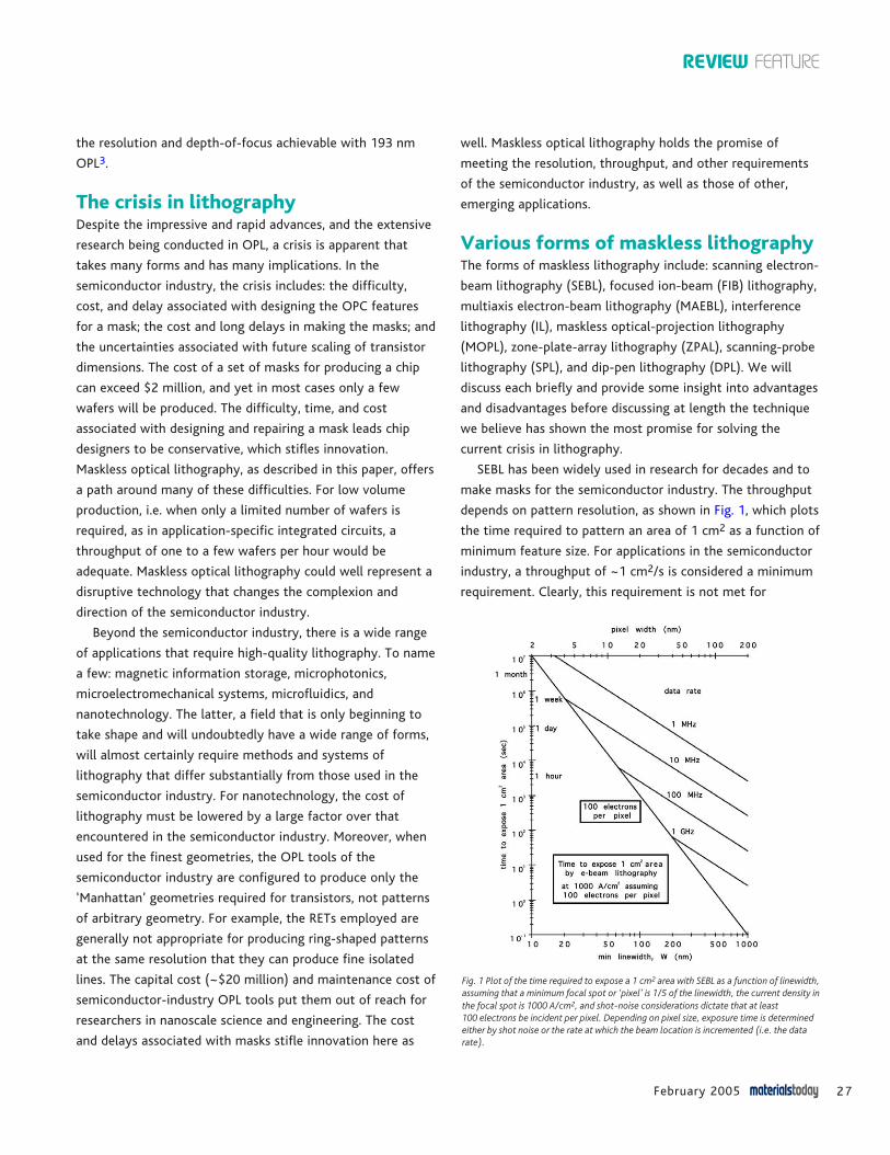
SEBL has been widely used in research for decades and to
make masks for the semiconductor industry. The throughput
depends on pattern resolution, as shown in Fig. 1, which plots
the time required to pattern an area of 1 cm2 as a function of
minimum feature size. For applications in the semiconductor
industry, a throughput of ~1 cm2/s is considered a minimum
requirement. Clearly, this requirement is not met for
REVIEW FEATURE
February 2005 27
Fig. 1 Plot of the time required to expose a 1 cm2 area with SEBL as a function of linewidth,
assuming that a minimum focal spot or ‘pixel’ is 1/5 of the linewidth, the current density in
the focal spot is 1000 A/cm2, and shot-noise considerations dictate that at least
100 electrons be incident per pixel. Depending on pixel size, exposure time is determined
either by shot noise or the rate at which the beam location is incremented (i.e. the data
rate).
linewidths below about 600 nm. MAEBL has been proposed as
a solution to this throughput problem4-7. However,
experimental results with such systems have been limited,
and commercial availability is uncertain.
Another problem with SEBL (and with all other forms of
electron or ion lithography) is pattern-placement accuracy.
Temperature gradients, stray electromagnetic fields, sample
charging, vibrations, and a variety of other effects cause the
electron beam to deviate from its intended position.
Conventional approaches attempt to limit the influence of
the disturbances via shielding, temperature control, vibration
isolation, and other means, all of which tend to escalate the
cost of systems. However, the placement accuracy is seldom
better than a few tens of nanometers, which is inadequate in
many applications. Another approach to solving the pattern-
placement problem is to form a feedback loop that controls
the beam position with reference to a fiducial grid on the
substrate that has long-range, spatial-phase coherence; a
technique called spatial-phase-locked electron-beam
lithography (SPLEBL)8,9. Placement accuracy approaching
1 nm has been demonstrated9. However, SPLEBL is still in the
development phase and not yet available commercially.
Implementation of spatial-phase locking in multibeam
systems has not been attempted.
FIB systems are capable of very high resolution10 but
suffer from worse problems of throughput and placement
accuracy than SEBL systems. IL has many forms11-14 and
throughput is quite high. However, it is applicable only to
periodic and quasiperiodic patterns, where it excels. SPL15
and DPL16 have a number of unique aspects and play an
important role in nanostructures research. However, they do
not appear to have the general applicability of optical
lithography techniques and lack sufficient throughput for
applications outside of research. A MOPL system has been
proposed that replaces the mask with a programmable
micromirror array17,18. We discuss this system below in
comparison to ZPAL.
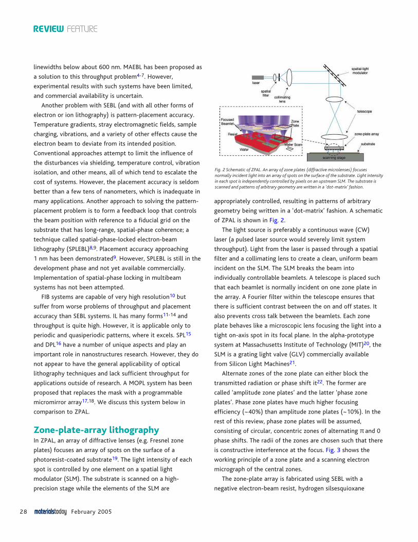
Zone-plate-array lithographyIn ZPAL, an array of diffractive lenses (e.g. Fresnel zone
plates) focuses an array of spots on the surface of a
photoresist-coated substrate19. The light intensity of each
spot is controlled by one element on a spatial light
modulator (SLM). The substrate is scanned on a high-
precision stage while the elements of the SLM are
appropriately controlled, resulting in patterns of arbitrary
geometry being written in a ‘dot-matrix’ fashion. A schematic
of ZPAL is shown in Fig. 2.
The light source is preferably a continuous wave (CW)
laser (a pulsed laser source would severely limit system
throughput). Light from the laser is passed through a spatial
filter and a collimating lens to create a clean, uniform beam
incident on the SLM. The SLM breaks the beam into
individually controllable beamlets. A telescope is placed such
that each beamlet is normally incident on one zone plate in
the array. A Fourier filter within the telescope ensures that
there is sufficient contrast between the on and off states. It
also prevents cross talk between the beamlets. Each zone
plate behaves like a microscopic lens focusing the light into a
tight on-axis spot in its focal plane. In the alpha-prototype
system at Massachusetts Institute of Technology (MIT)20, the
SLM is a grating light valve (GLV) commercially available
from Silicon Light Machines21.
Alternate zones of the zone plate can either block the
transmitted radiation or phase shift it22. The former are
called ‘amplitude zone plates’ and the latter ‘phase zone
plates’. Phase zone plates have much higher focusing
efficiency (~40%) than amplitude zone plates (~10%). In the
rest of this review, phase zone plates will be assumed,
consisting of circular, concentric zones of alternating π and 0
phase shifts. The radii of the zones are chosen such that there
is constructive interference at the focus. Fig. 3 shows the
working principle of a zone plate and a scanning electron
micrograph of the central zones.
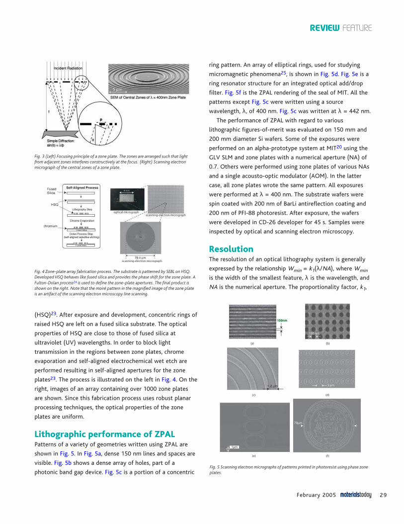
The zone-plate array is fabricated using SEBL with a
negative electron-beam resist, hydrogen silsesquioxane
REVIEW FEATURE
February 200528
Fig. 2 Schematic of ZPAL. An array of zone plates (diffractive microlenses) focuses
normally incident light into an array of spots on the surface of the substrate. Light intensity
in each spot is independently controlled by pixels on an upstream SLM. The substrate is
scanned and patterns of arbitrary geometry are written in a ‘dot-matrix’ fashion.
REVIEW FEATURE
(HSQ)23. After exposure and development, concentric rings of
raised HSQ are left on a fused silica substrate. The optical
properties of HSQ are close to those of fused silica at
ultraviolet (UV) wavelengths. In order to block light
transmission in the regions between zone plates, chrome
evaporation and self-aligned electrochemical wet etch are
performed resulting in self-aligned apertures for the zone
plates23. The process is illustrated on the left in Fig. 4. On the
right, images of an array containing over 1000 zone plates
are shown. Since this fabrication process uses robust planar
processing techniques, the optical properties of the zone
plates are uniform.
Lithographic performance of ZPALPatterns of a variety of geometries written using ZPAL are
shown in Fig. 5. In Fig. 5a, dense 150 nm lines and spaces are
visible. Fig. 5b shows a dense array of holes, part of a
photonic band gap device. Fig. 5c is a portion of a concentric
ring pattern. An array of elliptical rings, used for studying
micromagnetic phenomena25, is shown in Fig. 5d. Fig. 5e is a
ring resonator structure for an integrated optical add/drop
filter. Fig. 5f is the ZPAL rendering of the seal of MIT. All the
patterns except Fig. 5c were written using a source
wavelength, λ, of 400 nm. Fig. 5c was written at λ = 442 nm.
The performance of ZPAL with regard to various
lithographic figures-of-merit was evaluated on 150 mm and
200 mm diameter Si wafers. Some of the exposures were
performed on an alpha-prototype system at MIT20 using the
GLV SLM and zone plates with a numerical aperture (NA) of
0.7. Others were performed using zone plates of various NAs
and a single acousto-optic modulator (AOM). In the latter
case, all zone plates wrote the same pattern. All exposures
were performed at λ = 400 nm. The substrate wafers were
spin coated with 200 nm of BarLi antireflection coating and
200 nm of PFI-88 photoresist. After exposure, the wafers
were developed in CD-26 developer for 45 s. Samples were
inspected by optical and scanning electron microscopy.
ResolutionThe resolution of an optical lithography system is generally
expressed by the relationship Wmin = k1(λ/NA), where Wmin
is the width of the smallest feature, λ is the wavelength, and
NA is the numerical aperture. The proportionality factor, k1,
Fig. 3 (Left) Focusing principle of a zone plate. The zones are arranged such that light
from adjacent zones interferes constructively at the focus. (Right) Scanning electron
micrograph of the central zones of a zone plate.
February 2005 29
Fig. 4 Zone-plate array fabrication process. The substrate is patterned by SEBL on HSQ.
Developed HSQ behaves like fused silica and provides the phase shift for the zone plate. A
Fulton-Dolan process24 is used to define the zone-plate apertures. The final product is
shown on the right. Note that the moiré pattern in the magnified image of the zone plate
is an artifact of the scanning electron microscopy line scanning.
Fig. 5 Scanning electron micrographs of patterns printed in photoresist using phase zone
plates.
is empirically determined and accounts for process effects. In
OPL, as practiced in the semiconductor industry with
application of RETs, k1 values of 0.4 and above are
common26. Using phase zone plates operating at λ = 400 nm,
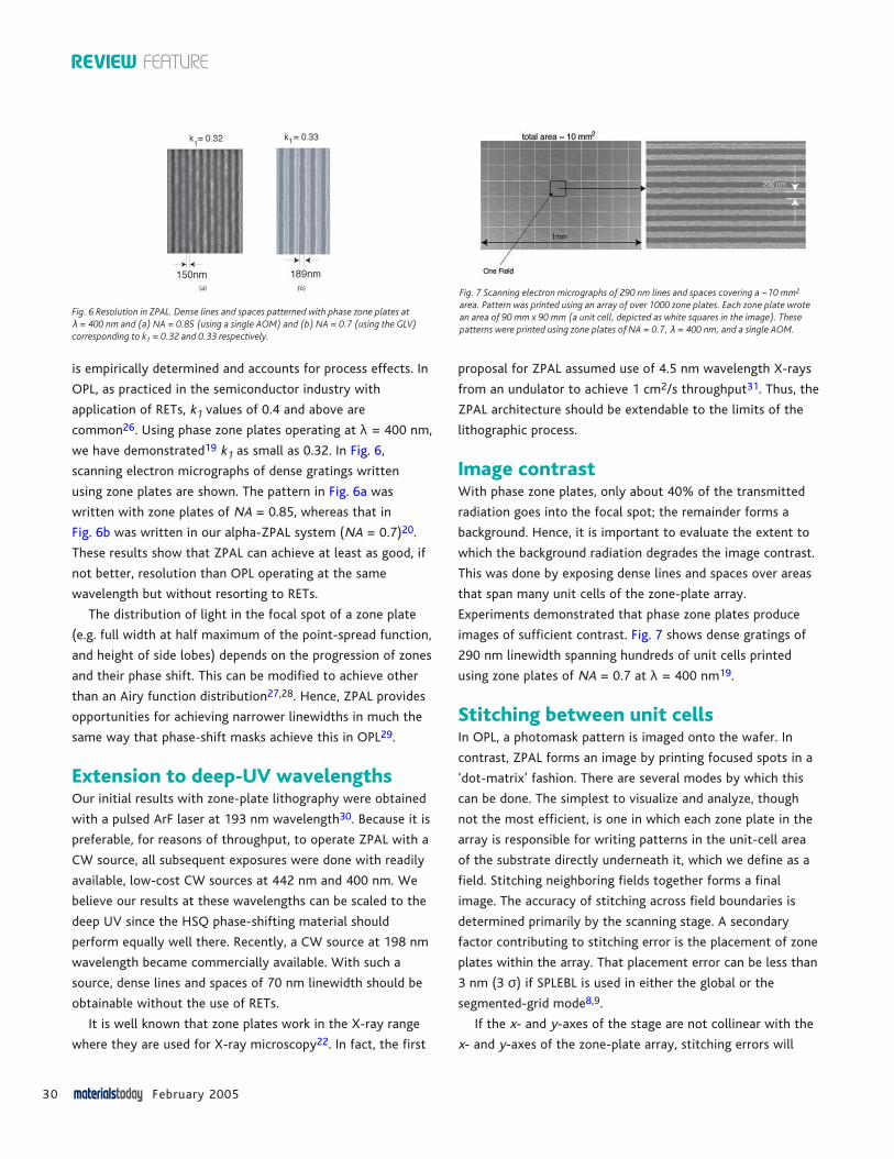
we have demonstrated19 k1 as small as 0.32. In Fig. 6,
scanning electron micrographs of dense gratings written
using zone plates are shown. The pattern in Fig. 6a was
written with zone plates of NA = 0.85, whereas that in
Fig. 6b was written in our alpha-ZPAL system (NA = 0.7)20.
These results show that ZPAL can achieve at least as good, if
not better, resolution than OPL operating at the same
wavelength but without resorting to RETs.
The distribution of light in the focal spot of a zone plate
(e.g. full width at half maximum of the point-spread function,
and height of side lobes) depends on the progression of zones
and their phase shift. This can be modified to achieve other
than an Airy function distribution27,28. Hence, ZPAL provides
opportunities for achieving narrower linewidths in much the
same way that phase-shift masks achieve this in OPL29.
Extension to deep-UV wavelengthsOur initial results with zone-plate lithography were obtained
with a pulsed ArF laser at 193 nm wavelength30. Because it is
preferable, for reasons of throughput, to operate ZPAL with a
CW source, all subsequent exposures were done with readily
available, low-cost CW sources at 442 nm and 400 nm. We
believe our results at these wavelengths can be scaled to the
deep UV since the HSQ phase-shifting material should
perform equally well there. Recently, a CW source at 198 nm
wavelength became commercially available. With such a
source, dense lines and spaces of 70 nm linewidth should be
obtainable without the use of RETs.
It is well known that zone plates work in the X-ray range
where they are used for X-ray microscopy22. In fact, the first
proposal for ZPAL assumed use of 4.5 nm wavelength X-rays
from an undulator to achieve 1 cm2/s throughput31. Thus, the
ZPAL architecture should be extendable to the limits of the
lithographic process.
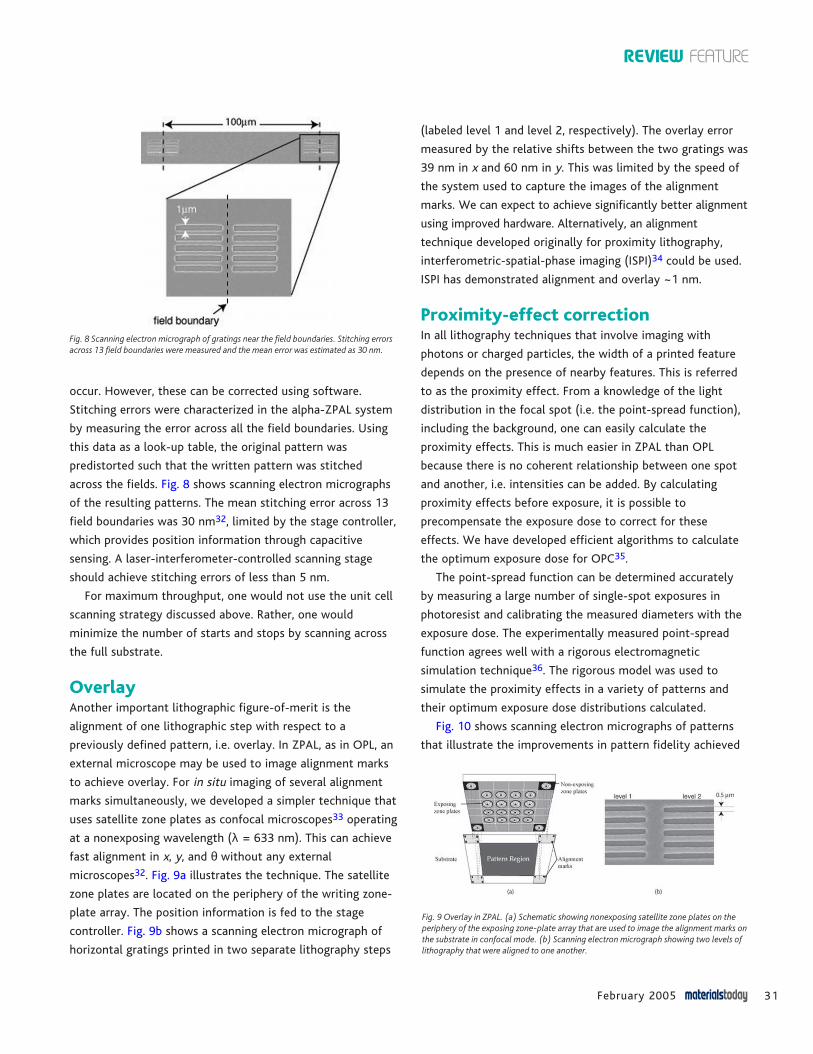
Image contrastWith phase zone plates, only about 40% of the transmitted
radiation goes into the focal spot; the remainder forms a
background. Hence, it is important to evaluate the extent to
which the background radiation degrades the image contrast.
This was done by exposing dense lines and spaces over areas
that span many unit cells of the zone-plate array.
Experiments demonstrated that phase zone plates produce
images of sufficient contrast. Fig. 7 shows dense gratings of
290 nm linewidth spanning hundreds of unit cells printed
using zone plates of NA = 0.7 at λ = 400 nm19.
Stitching between unit cellsIn OPL, a photomask pattern is imaged onto the wafer. In
contrast, ZPAL forms an image by printing focused spots in a
‘dot-matrix’ fashion. There are several modes by which this
can be done. The simplest to visualize and analyze, though
not the most efficient, is one in which each zone plate in the
array is responsible for writing patterns in the unit-cell area
of the substrate directly underneath it, which we define as a
field. Stitching neighboring fields together forms a final
image. The accuracy of stitching across field boundaries is
determined primarily by the scanning stage. A secondary
factor contributing to stitching error is the placement of zone
plates within the array. That placement error can be less than
3 nm (3 σ) if SPLEBL is used in either the global or the
segmented-grid mode8,9.
If the x- and y-axes of the stage are not collinear with the
x- and y-axes of the zone-plate array, stitching errors will
REVIEW FEATURE
February 200530
Fig. 7 Scanning electron micrographs of 290 nm lines and spaces covering a ~10 mm2
area. Pattern was printed using an array of over 1000 zone plates. Each zone plate wrote
an area of 90 mm x 90 mm (a unit cell, depicted as white squares in the image). These
patterns were printed using zone plates of NA = 0.7, λ = 400 nm, and a single AOM.
Fig. 6 Resolution in ZPAL. Dense lines and spaces patterned with phase zone plates at
λ = 400 nm and (a) NA = 0.85 (using a single AOM) and (b) NA = 0.7 (using the GLV)
corresponding to k1 = 0.32 and 0.33 respectively.
REVIEW FEATURE
occur. However, these can be corrected using software.
Stitching errors were characterized in the alpha-ZPAL system
by measuring the error across all the field boundaries. Using
this data as a look-up table, the original pattern was
predistorted such that the written pattern was stitched
across the fields. Fig. 8 shows scanning electron micrographs
of the resulting patterns. The mean stitching error across 13
field boundaries was 30 nm32, limited by the stage controller,
which provides position information through capacitive
sensing. A laser-interferometer-controlled scanning stage
should achieve stitching errors of less than 5 nm.
For maximum throughput, one would not use the unit cell
scanning strategy discussed above. Rather, one would
minimize the number of starts and stops by scanning across
the full substrate.
OverlayAnother important lithographic figure-of-merit is the
alignment of one lithographic step with respect to a
previously defined pattern, i.e. overlay. In ZPAL, as in OPL, an
external microscope may be used to image alignment marks
to achieve overlay. For in situ imaging of several alignment
marks simultaneously, we developed a simpler technique that
uses satellite zone plates as confocal microscopes33 operating
at a nonexposing wavelength (λ = 633 nm). This can achieve
fast alignment in x, y, and θ without any external
microscopes32. Fig. 9a illustrates the technique. The satellite
zone plates are located on the periphery of the writing zone-
plate array. The position information is fed to the stage
controller. Fig. 9b shows a scanning electron micrograph of
horizontal gratings printed in two separate lithography steps
(labeled level 1 and level 2, respectively). The overlay error
measured by the relative shifts between the two gratings was
39 nm in x and 60 nm in y. This was limited by the speed of
the system used to capture the images of the alignment
marks. We can expect to achieve significantly better alignment
using improved hardware. Alternatively, an alignment
technique developed originally for proximity lithography,
interferometric-spatial-phase imaging (ISPI)34 could be used.
ISPI has demonstrated alignment and overlay ~1 nm.
Proximity-effect correctionIn all lithography techniques that involve imaging with
photons or charged particles, the width of a printed feature
depends on the presence of nearby features. This is referred
to as the proximity effect. From a knowledge of the light
distribution in the focal spot (i.e. the point-spread function),
including the background, one can easily calculate the
proximity effects. This is much easier in ZPAL than OPL
because there is no coherent relationship between one spot
and another, i.e. intensities can be added. By calculating
proximity effects before exposure, it is possible to
precompensate the exposure dose to correct for these
effects. We have developed efficient algorithms to calculate
the optimum exposure dose for OPC35.
The point-spread function can be determined accurately
by measuring a large number of single-spot exposures in
photoresist and calibrating the measured diameters with the
exposure dose. The experimentally measured point-spread
function agrees well with a rigorous electromagnetic
simulation technique36. The rigorous model was used to
simulate the proximity effects in a variety of patterns and
their optimum exposure dose distributions calculated.
Fig. 10 shows scanning electron micrographs of patterns
that illustrate the improvements in pattern fidelity achieved
February 2005 31
Fig. 8 Scanning electron micrograph of gratings near the field boundaries. Stitching errors
across 13 field boundaries were measured and the mean error was estimated as 30 nm.
Fig. 9 Overlay in ZPAL. (a) Schematic showing nonexposing satellite zone plates on the
periphery of the exposing zone-plate array that are used to image the alignment marks on
the substrate in confocal mode. (b) Scanning electron micrograph showing two levels of
lithography that were aligned to one another.
by performing the optimization. The original pattern (Fig. 10,
left) received uniform exposure dose throughout, whereas the
optimized pattern (Fig. 10, right) received an optimized
exposure dose distribution. It was also observed that the
optimized pattern was more robust to exposure dose
variations, i.e. had higher exposure latitude compared to the
original pattern.
This optimization is analogous in its effect to the OPC
techniques used in OPL. However, the problem is
computationally much simpler with ZPAL because a pattern is
formed by an incoherent addition of focused spots, i.e. one
adds intensities. In OPL the entire image is formed at the
same time and hence one must compute the total field
created by radiation from all components of a mask pattern
and then square that field distribution to obtain the intensity
distribution that exposes the resist. This is a much more
daunting task and in fact it cannot be solved in closed form;
empirical information must supplement the computation.
ThroughputLithography can be viewed as an information transfer process
where the information content on a substrate is proportional
to the number of independent pixels per unit area. In OPL,
the information stored on a photomask (which amounts to
~1011-1012 bits) is transferred onto the substrate in parallel,
typically with an exposure time of order 1 s. This high
throughput is crucial to the business model of the
semiconductor industry. However, the high throughput is
achieved at the expense of flexibility and very high cost.
A maskless lithography system such as ZPAL provides
flexibility and saves photomask costs at the expense of lower
throughput. In ZPAL, the rate of information transfer is the
product of the number of zone plates in the array and the
switching speed of the SLM. The current SLM has 1088
switching elements and can operate at 0.5 MHz. With that
switching speed, 1000 zone plates, and 8 bits per pixels (for
‘gray toning’), the information transfer rate is 4 x 109 bits/s.
The GLV-type SLM can be modified37 to operate up to
~5 MHz. A SLM of 5000 element illuminating 5000 zone
plates, with 8 bits per pixel would result in an information
transfer rate of 2 x 10¹¹, or several wafers per hour; about a
factor of ten slower than OPL but at least two orders of
magnitude faster than SEBL for the same focal spot diameter,
as can be seen in Fig. 1. Moreover, with photons, shot noise is
orders of magnitude less severe and the particles do not
interact. Electrostatic interactions limit the flux in electron-
beam systems.
Comparison to maskless opticalprojection lithographyMOPL in which the photomask is replaced by an SLM
consisting of an array of micromirrors is being developed17,18.
The pattern on the SLM is controlled digitally, and its image
is projected onto a wafer by means of a reduction lens.
MOPL utilizes a high-power pulsed laser source whose rate
(~kHz) limits the switching speed of the SLM. In order to
achieve sufficient throughput, the number of pixels in the
SLM has to be inordinately large, e.g. 2048 x 5120 (over ten
million). This is a daunting challenge. Since a CW laser source
can be used in ZPAL, the smaller number of pixels (and zone
plates) is compensated by the much higher switching speed
achieved by a fast GLV-based SLM.
In MOPL, several pixels on the SLM are used to print a
single pixel in the image on the wafer. This is required to
ensure the fidelity of images and to enable the equivalent of
phase-shift masks. Since each pixel on a typical SLM is several
microns in size, this puts a major burden for demagnification
on the refractive optics of the MOPL system. For example, in
the commercially proposed system, nine pixels, each of size
8 µm x 8 µm, are used to print one pixel of size 90 nm on the
wafer. This requires a demagnification factor of 267, which is
higher than any optical microscope lens and probably difficult
to achieve with full-image aberration correction. This large
demagnification will likely complicate the problem of
alignment. The use of refractive optics means that MOPL
cannot be extended to wavelengths shorter than 157 nm. In
contrast, in ZPAL, the light from one pixel on the SLM is
focused to a spot on the substrate by one zone plate. Hence,
REVIEW FEATURE
February 200532
Fig. 10 Scanning electron micrographs of pattern showing improvements from OPC. (Left)
Exposure dose was uniform within the pattern. (Right) An optimum exposure dose was
used. Patterns were exposed using zone plates at λ = 400 nm, NA = 0.7, and an AOM.
REVIEW FEATURE
the issue of demagnification does not arise. Since zone plates
focus on axis without aberration, the resulting image in ZPAL
is always aberration free. Moreover, diffractive optics can
operate at extreme-UV and X-ray wavelengths.
Analog control of SLM pixels is used in MOPL to achieve
sufficient pattern-placement accuracy and pattern fidelity.
This requires a transistor and storage capacitor for each pixel
in the SLM, which is extremely difficult when the number of
pixels is large (around ten million). Furthermore, the response
characteristic of each pixel is different and separate
correction must be applied to each pixel, increasing the
complexity of the system.
In MOPL, one field of the pattern is projected at one time.
Then the substrate is scanned before the next field is printed.
The stage has to scan the length equivalent to the side of the
field, resulting in much larger scan speeds compared to ZPAL,
where the stage moves from one spot to another, typically
only about 50-100 nm.
Finally, MOPL requires OPC essentially the same as in OPL.
Because of the partially coherent nature of the imaging
process, the proximity correction is orders of magnitude more
difficult to achieve than in ZPAL, where the imaging is
completely incoherent (see Fig. 10).
ConclusionIL and SEBL represent highly effective forms of maskless
lithography, especially for research and low-volume, special
purpose manufacturing. SEBL can write patterns of arbitrary
geometry but suffers from problems of low throughput, high
cost, and pattern placement inaccuracy. Two forms of
maskless optical lithography have been described, MOPL and
ZPAL. The latter has demonstrated the highest quality
lithographic results ever reported at 400 nm wavelength and
has a clear path to shorter wavelengths, higher resolution,
higher throughput, low cost, and commercial availability38.
ZPAL is an entirely new paradigm that promises to
circumvent many of the problems that have troubled OPL
and will likely be encountered by MOPL. We believe that
ZPAL has the potential to enable low-cost, flexible, high-
quality patterning for a wide variety of applications in the
field of micro- and nanotechnology. MT
AcknowledgmentsThe authors would like to thank David Carter, Mark Mondol, Jim Daley, Jim Carter,
Fernando Castaño, Euclid Moon, Wonjoon Jung, and George Barbastathis for various
contributions to this work. This research was partially funded by DARPA and the Army
Research Office under Grant No. DAAD19-01-1-0330.
February 2005 33
REFERENCES
1. Valiev, K. A., The Physics of Submicron Lithography, Plenum Press, New York,
(1992)
2. See, for example, Proceedings of Annual SPIE Symposia on Microlithography
3. Owa, S., and Nagasaka, H., J. Microlitho. Microfab. Microsys. (2004) 3 (1), 97;
Switkes, M., et al., J. Vac. Sci. Technol. B (2003) 21 (6), 2794
4. Pease, R. F., Charged Particle Maskless Lithography, Presented at 30th
International Conference on Micro & Nano Engineering 2004, to be published
Microelectron. Eng.
5. Groves, T. R., and Kendall, R. A., J. Vac. Sci. Technol. B (1998) 16 (6), 3168
6. Pickard, D. S., et al., J. Vac. Sci. Technol. B (2002) 20 (6), 2662
7. Muraki, M., and Gotoh, S., J. Vac. Sci. Technol. B (2000) 18 (6), 3061
8. Hastings, J. T., et al., J. Vac. Sci. Technol. B (2002) 20 (6), 2753
9. Hastings, J. T., et al., J. Vac. Sci. Technol. B (2003) 21 (6), 2650
10. Atkinson, G. M., et al., J. Vac. Sci. Technol. B (1992) 10 (6), 3104
11. Walsh, M. E., and Smith, H. I., J. Vac. Sci. Technol. B (2001) 19 (6), 2347
12. Savas, T. A., et al., J. Vac. Sci. Technol. B (1996) 14 (6), 4167
13. Walsh, M. E., et al., J. Vac. Sci. Technol. B (2000) 18 (6), 3539
14. Konkola, P., et al., J. Vac. Sci. Technol. B (2003) 21 (6), 3097
15. Kramer, S., et al., Chem. Rev. (2003) 103 (11) 4367
16. Ginger, D. S., et al., Angew. Chem. Int. Ed. (2003) 43 (11), 30
17. Sandstrom, T., et al., Proc. SPIE (2004) 5377 (2), 777
18. Choksi, N., et al., J. Vac. Sci. Technol. B (1999) 17 (6), 3047
19. Gil, D., et al., J. Vac. Sci. Technol. B (2003) 21 (6), 2810
20. Menon, R., et al., J. Vac. Sci. Technol. B (2004), in press
21. Bloom, D. M., Proc. SPIE (1997), 3013, 165
22. Michette, A. G., Optical Systems for Soft X-rays, Plenum Press, New York,
(1986)
23. Gil, D., et al., J. Vac. Sci. Technol. B (2003) 21 (6), 2956
24. Fulton, T. A., and Dolan, G. J., Appl. Phys. Lett. (1983) 42 (8) 752
25. Castano, F. J., et al., J. Vac. Sci. Technol. B (2004), in press
26. Finders, J., et al., Proc. SPIE (2000) 4226, 1
27. Cao, Q., and Jahns, J., J. Opt. Soc. Am. A (2003) 20 (8), 1576
28. Kipp, L., et al., Nature (2001) 414, 184
29. Barbastathis, G., et al., Zone plate array optimization for maskless lithography.
To be presented at the 2nd International Conference on Advanced Materials
and Nanotechnology, Queenstown, New Zealand, 2005
30. Djomehri, I., et al., J. Vac. Sci. Technol. B (1998) 16 (6), 3426
31. Smith, H. I., J. Vac. Sci. Technol. B (1996) 14 (6), 4318
32. Menon, R., et al., J. Vac. Sci. Technol. B (2004), in press
33. Gil, D., et al., J. Vac. Sci. Technol. B (2000) 18 (6), 2881
34. Moon, E., et al., J. Vac. Sci. Technol. B (2003) 21 (6), 3112
35. Menon, R., Diffractive Optics for Maskless Lithography and Imaging, PhD
dissertation, Massachusetts Institute of Technology, Cambridge, MA, (2003)
36. Prather, D. W., and Shouyuan, S., J. Opt. Soc. Am. A (1999) 16 (5), 1131
37. Payne, A., et al., Proc. SPIE (2004) 5348, 76
38. See www.lumarray.com


