Embed Size (px)
Citation preview

Microcontroller with Transponder Interface
U9280M-H
Preliminary
Rev. 4591A–RFID–03/03
Features• 4-bit HARVARD Architecture• 4 k ��8-bit Application ROM• 256 ��4-bit RAM• 32 ��16-bit EEPROM• 10 Bi-directional I/Os• 4 External Interrupt Inputs (SSO20)• 8 Interrupt Levels• 2 ��8-bit Multifunction Timer/Counter• Interval Timer with Watchdog• Two-Wire Interface (TWI) • Voltage Supervisor• On-chip RC Oscillator• On-chip Crystal Oscillator
Benefits• Contactless Power Supply and Communication Interface • Power Management for Contactless and Battery Power Supply• Shift-register-supported Modulator and Demodulator Stages• Low Power Consumption• Active Mode < 300 µA at 2 V and 1 MHz System Clock Frequency
(2 µs Instruction Cycle)• Power-down Mode < 1 µA• Supply Voltage 2.0 V to 6.5 V • High-level Language Programming in qFORTH• Operating Speed: 1 µs to 10 µs Instruction Cycle (2 µs at VDD = 2 V)
DescriptionThe U9280M-H IC is a multi-chip module for remote control and contactless ID sys-tems. It consists of the ATAR092 microcontroller and U3280M transponder interfacecircuit with EEPROM. A coil connected to the transponder interface serves as a wire-less bi-directional communication interface as well as a power supply for themicrocontroller and the interface. As a transponder, the device is supplied by a mag-netic RF field applied at the coil. For IR- or RF-transmitter applications, it can besupplied by a battery. The microcontroller supports, with its built-in timers, a widerange of IR- and RF-transmission modes such as burst-modulation modes, PWM-,NRZ-, Manchester- and Bi-phase coding.
1

Figure 1. Block Diagram
Pin Configuration
Figure 2. Pinning SSO20
Dampingstage
512-bitEEPROMmemory
U9280M-H transponder interface
COIL1
COIL2
VSS
ATAR092 microcontroller
OSC2 OSC1/ROSC
BP60/T3O
RAM
Rectifier
VDD
Field/GAP detect
VBATT
MOD
NGAP
BP42/T2O
BP63/T3I
BP23
BP53/INT1
BP40/SC/INT3
BP50/INT6
BP41/VMI/ T2I
BP43/SD/INT3
Timer/counter
C
Biphasemodulator
ROM
voltage monitorReset
BP20/NTE
Serial interface
Clockextractor
FC
Power management
4-bit CPU core
MCL
I/O-Ports
Serial interface
Modulator/demodulator
Oscillatorsclock management
�1
VDD
BP40/SC/INT3
BP50/INT6
BP53/INT1
OSC1/ROSC
OSC2
BP60/T3O
BP41/VMI
BP43/SD/INT3
BP42/T2O
VSS
BP63/T3I/INT5
BP20/NTE
BP23
COIL1
VBATT
MODCOIL2
NGAP
U9280M-H
1
2
3
4
5
6
7
8
9
10 11
12
13
14
15
16
17
18
19
20
FC
2 U9280M-H 4591A–RFID–03/03

U9280M-H
Pin DescriptionPin Symbol Function
1 COIL1 Coil input 1, Pin to connect an LC antenna for communication and field supply
2 COIL2 Coil input 2, Pin to connect an LC antenna for communication and field supply
3 VBATT Power-supply voltage input to connect a battery
4 VDDPower-supply voltage for the microcontroller and EEPROM. At this pin a capacitor (0.5 µF to 10 µF) must be connected to buffer the voltage during field supply and to block the VDD of the microcontroller.
5 BP40/SC/INT3 I/O-port line/serial clock line/INT3 input (falling edge sensitive)
6 BP53/INT3 I/O-port line/INT3 interrupt input (falling or rising edge sensitive)
7 BP50/INT6 I/O-port line/INT6 interrupt input (falling or rising edge sensitive)
8 OSC1/ROSC Oscillator- or external system-clock input/input for RC-oscillator resistor
9 OSC2 Oscillator output
10 BP60/T3O Bi-directional I/O-line/Timer 3 output/modulator output
11 BP63/T3I/INT5 I/O-port line/INT5 interrupt input/Timer 3 input/demodulator input
12 BP20/NTEBP20-I/O-port line/test mode input. This input is used to control the test modes. During POR it must not be connected with a low impedance to VDD.
13 BP23 I/O-port line
14 BP41/VMI I/O-port line/Voltage monitor input/Timer 2 input
15 BP42/T2O I/O-port line/Timer 2 output/modulator output
16 BP43/SD/INT3 I/O-port line/serial data line/INT3 input (falling edge sensitive)
17 VSS Circuit ground
18 FC Field clock output of the clock extractor
19 MOD Modulation input - front end. Must be connected to the modulator output T2O.
20 NGAP Gap detect output - front end. Must be connected to the demodulator input T3I.
34591A–RFID–03/03

Functional Description
The U9280M-H multi-chip module contains a microcontroller and a transponder ICmounted in a single package. Everything necessary for remote control and wirelessidentifcation systems is integrated: Inputs to connect keys, outputs to control an IR- orRF transmitter and to drive indicator LEDs, an EEPROM to store key code and identifi-ers, and an interface for contactless communication and a power supply.
The U3280M is a transponder interface consisting of an analog front end for contactlessdata communication and power supply, and a serial 512-bit EEPROM. In addition, itincludes power management to switch the battery or magnetic-field power supply. Formodulation and demodulation of the magnetic field, the device has input and output pinsto connect the microcontroller. The MOD, NGAP and FC Pins can be connected exter-nally to the modulator, demodulator and timer I/O pins of the microcontroller. Access tothe EEPROM is possible via a two-wire serial interface. The ATAR092 microcontrollersare equipped with compatible two-wire serial interface to communicate with theU3280M. In the U9280M-H the serial interfaces of the transponder interface and themicrocontroller are linked internally.
ATAR092 The ATAR092 microcontroller is a member of the Atmel’s 4-bit single-chip microcontrol-ler family. It is especially designed for remote-control applications. It consists of anadvanced stack-based 4-bit CPU core with 4 K ROM, 256 nibble of RAM and on-chipperipherals. The CPU is based on the HARVARD architecture and contains an interruptcontroller with 8 prioritized interrupt levels.
The peripherals include parallel I/O ports, two 8-bit programmable multifunctiontimer/counters, a two-wire serial interface, an interval timer with watchdog function anda voltage supervisor. The serial interface supports, together with the timers, a modulatorand demodulator stage for Manchester, Bi-phase and pulse-width modulation anddemodulation. The integrated clock generator contains a RC-, a 32-kHz crystal, a4-MHz crystal oscillator and a programmable input to use an external clock.
Note: In the U9280M-H not all I/O pins of the ATAR092 are available (see “Pin Description”).The microcontroller is fully described in the MARC4 ATAR092 data sheet.
4 U9280M-H 4591A–RFID–03/03

U9280M-H
Figure 3. Block Diagram ATAR092
The U3280M Transponder Interface
The transponder interface contains a rectifier stage to rectify the AC from the coil inputsand to supply itself and an additional microcontroller device with power from an LC-res-onant circuit at the coil inputs. It is also possible to supply the device via the VBatt -inputwith DC from a battery. The built-in power management switches automatically betweenbattery supply (VBatt pin) and coil supply. It switches to coil supply if a field is applied atthe coil and switches back to battery if the field is removed.
The voltage from the coil or the VBatt pin is output at the VDD pin to supply the microcon-troller device. At the VDD pin a capacitor must be connected to smooth and buffer thesupply voltage for the transponder interface and the microcontroller. This capacitor isalso used to buffer the supply voltage during communication (damping and gaps in thefield).
For communication, a damping-stage and a gap-detect circuitry is on the chip. Bymeans of the damping stage the coil voltage can be modulated to transmit data via thefield. It can be controlled with the modulator input (MOD pin) via the microcontroller. Thegap detection circuitry detects gaps in the field and outputs the gap/field signal at thegap detect output (NGAP pin). It can be used to receive data via a modulated field andto check if a field is applied at the coil.
For the storage of data such as key codes, identifiers and configuration bits, a 512-bitEEPROM is available on the chip. It can be read and written to by the microcontroller viaa TWI-compatible two-wire serial interface. The serial interface, the EEPROM and themicrocontroller are supplied with the voltage at the VDD pin. That means the microcon-troller can read and write to the EEPROM if the supply voltage is in the operating range.
Voltage monitor External input
MARC4
UTCM
OSC1 OSC2
I/O bus
ROM RAM
4-bit CPU core
256 x 4 bit
VDDV SS
Data direction +alternate function
Data direction +interrupt control
Port 4 Port 5
Data dir. +alt. function
Port 6
Timer 3
Brown-out protect RESET
Clock managementTimer 1
watchdog timer
Timer 2
Serial interface
Port 1
Por
t 2
Dat
a di
rect
ion
T2O
SD
SC
T3O
T3I
BP10
BP13
BP20/NTE
BP21
BP22
BP23
BP40INT3 SC BP41
VMI T2I
BP42 T2O BP43
INT3 SD
BP50INT6
BP51INT6
BP52INT1
BP53INT1
BP60 T3O
BP63 T3I
RCoscillators
Crystaloscillators
4 K x 8-bit
VMI
with modulator
SSI
Externalclock input
interval- and
8/12-bit timer
8-bittimer / counterwith modulator
and demodulator
T2I
54591A–RFID–03/03

The U3280M contains additional operating modes to support a wide range of applica-tions. These modes can be controlled via the serial interface. The power managementcan be switched off by software to disable the automatic switching between battery andfield. This supports applications with battery supply only.
There is an on-chip Bi-phase and Manchester modulator. It can be selected and con-trolled via the serial interface with a special mode control byte. If this modulator is usedthe external connection to the modulator input is not necessary.
Modulation The transponder interface can modulate the magnetic field by a modulator to transmitdata to a base station. It modulates the coil voltage by varying the coil‘s load. The mod-ulator can be controlled via the MOD pin. A high level 1 increases the current into thecoil inputs and damps the coil voltage. A low level 0 decreases the current andincreases the coil voltage. The modulator generates a voltage stroke of about 2 Vpp atthe coil. A high level at the MOD input makes the maximum of the field energy availableat VDD. During a reset a high level at the MOD input causes the optimum conditions forstarting the device and charging the capacitor at VDD after the field is applied at the coil.
Digital Input to Control the Damping Stage (MOD)
Mod = 0: coil undamped
Mod = 1: coil damped
VCMS = VCID: modulation voltage stroke at coil inputs
Note: If the automatic power management is disabled the internal front end VDD is limited atVDDC. In this case the value VDDC must be used in the formula above.
Field Clock The field clock extractor of the interface makes the field clock available for the microcon-troller. It can be used to supply timer inputs to synchronize modulation anddemodulation with the field clock.
Gap Detect The transponder interface can also receive data. The base station modulates the datawith short gaps in the field. The gap-detection circuit detects these gaps in the magneticfield and outputs the gap/field signal at the NGAP pin. A high level indicates that a fieldis applied at the coil and a low level indicates a gap or that the field is off. The microcon-troller must demodulate the incoming data stream at one of its inputs.
Digital Output of the Gap Detection Stage (NGAP)
NGAP = 0: gap detected/no fieldVCOIL_peak = VFDOFF
NGAP = 1: field detectedVCOIL_peak = VFDON
Note: No amplifier is used in the gap detection stage. A digital Schmitt trigger evaluates therectified and smoothed coil voltage.
VCOIL_peak VDD 2 VCMS+� VCU= =
VCOIL_peak VDD 2� VCD= =
6 U9280M-H 4591A–RFID–03/03

U9280M-H
Wake-up Signal If a field is applied at the coil of the transponder interface the microcontroller can bewoken up with the wake signal at the NGAP pin. For that purpose the NGAP pin must beconnected to an interrupt input of the microcontroller. A high level at the NGAP outputindicates an applied field and can be used as a wake signal for the microcontroller viaan interrupt. If no battery voltage is available at VBatt the controller starts with a power-on-reset after the voltage of the buffer capacitor at VDD is loaded by the field above thepower-on-reset level.
The wake signal is generated if the power management switches to field supply. Thefield detection stage of the power management has low-pass characteristics to avoid thegeneration of wake signals and unnecessary switching between battery and field supplyin case of interferences at the coil inputs.
U3280M Signals and Timing
Figure 4. Modulation
Figure 5. Gap Detection and Battery to Field Switching
Power Supply The U3280M has a power management that handles two power-supply sources. Nor-mally, the IC is supplied by a battery at the VBatt pin. If a magnetic field is applied at theLC-resonant circuit of the device the field detection circuit switches from VBatt to fieldsupply. During field supply the VDD voltage is limitted to 3 V.
The VDD pin is used to connect a capacitor to smooth the voltage from the rectifier andto buffer the power when the field is modulated by gaps and damping. The EEPROMand the microcontroller always operate with the voltage at the VDD pin.
VCU
VCDVCMS
MOD
Coil inputs
VFDON
VFDOFF
tFBS
tBFS
Coil supply if automatically power management is enabled
Battery
supplyBattery
supply
Coil inputs
NGAP
Field clock FC
Power management
1. edge used as wakeup signal
tFGAP1 t FGAP0
VFDON
VFDOFF
t FBSt BFS
Coil supply if automatically power management is enabledBatterysupply
Batterysupply
Coil inputs
NGAP
Field clock FC
Power management
1. edge used as wakeup signal
tFGAP1 t FGAP0
74591A–RFID–03/03

Automatic Power Management
There are different conditions to switch from the battery to field generated voltage andvice versa.
Figure 6. Switch Conditions for Power Management
The power management switches automatically from battery to field if the rectified volt-age (Vcoil) from the coil inputs becomes higher than field-on-detection voltage (VFDON)even if no battery voltage is available (0 < VBatt < 1.8 V). It switches back to battery if thecoil voltage becomes lower than the field-off-detection voltage (VFDOFF).
The field-detection stage of the power management has low-pass characteristics to sup-press noise. An applied field needs a time delay tBFS (battery-to-field switch delay) tochange the power supply. If the field is removed from the coil the power managementwill generate a reset of the microcontroller.
Controlling Power Management via the Serial Interface
The automatic mode of the power management can be switched off and on by a com-mand from the microcontroller. If the automatic mode is switched off the IC is alwayssupplied by the battery up to the next power-on reset or to a switch-on command. Thepower management-on and -off command must be transferred via the serial interface.
If the power management is switched off and the device is supplied from the battery itcan communicate via the field without loading the field. This mode can be used to real-ize applications with a battery supply if the available field is too weak to supply the ICwith power.
Buffer Capacitor CB The buffer capacitor connected at VDD is used to buffer the supply voltage for the micro-controller and the EEPROM during field supply. It smooths the rectified AC from the coiland buffers the supply voltage during modulation and gaps in the field. The size of thiscapacitor depends on the application. It must be of a dimension so that during modula-tion and gaps the ripple on the supply voltage is in the range of 100 to 300 mV. Duringgaps and damping the capacitor is used to supply the device, that means the size of thecapacitor depends on the length of the gaps and damping cycles.
Example: For a supply current of 350 µA, 200 mV ripple at VDD
Table 1. Buffer Capacitor
Batterysupply
Fieldsupply(VBatt)
VCoil < VFDON for t > tFBS
VCoil < VFDOFF for t > tFBS
Time with no Field Supply Necessary CB
250 µs 470 nF
500 µs 1000 nF
8 U9280M-H 4591A–RFID–03/03

U9280M-H
Serial Interface The transponder interface has an serial interface to the microcontroller for read andwrite accesses to the EEPROM. In a special mode the serial interface can also be usedto control the Bi-phase/Manchester modulator or the power management of theU3280M.
The serial interface of the U3280M device must be controlled by a master device (nor-mally the ATAR09x microcontroller) which generates the serial clock and controls theaccess via the SCL- and SDA-line. SCL is used to clock the data in and out of thedevice. SDA is a bi-directional line used to transfer data into and out of the device. Thefollowing protocol is used for data transfers.
Serial Protocol • Data states on the SDA line changing only while SCL is low.
• Changes in the SDA line while SCL is high will be interpreted as a START or STOP condition.
• A START condition is defined as a high-to-low transition on the SDA-line while the SCL-line is high.
• A STOP condition is defined as a low-to-high transition on the SDA-line while the SCL-line is high.
• Each data transfer must be initialized with a START condition and terminated with a STOP condition. The START condition wakes the device from standby mode and the STOP condition returns the device to stand-by mode.
• A receiving device generates an acknowledge (A) after the reception of each byte. For that the master device must generate an extra clock pulse. If the reception was successful the receiving master or slave device pulls down the SDA-line during that clock cycle. If in transmit mode an acknowledge is not detected (N) by the interface, it will terminate further data transmissions and will go into receive mode. A master device must finish its read operation by a Not-acknowledge and then issue a stop condition to place the device into a known state.
Figure 7. Serial Protocol
Startcondition
Datavalid
Datachange
Data/acknowledge
valid
Stopcondition
SCL
SDA
Stand-by
Stand-by
94591A–RFID–03/03
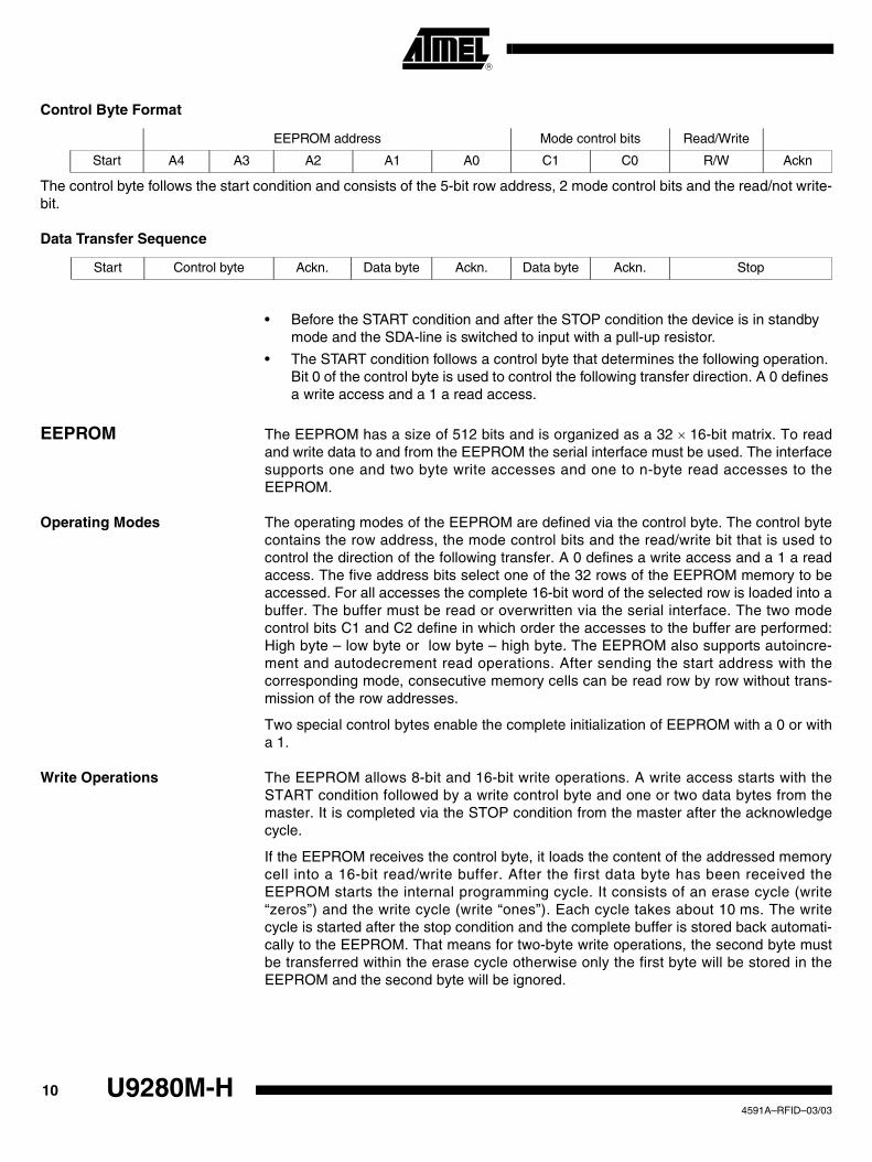
Control Byte Format
The control byte follows the start condition and consists of the 5-bit row address, 2 mode control bits and the read/not write-bit.
Data Transfer Sequence
• Before the START condition and after the STOP condition the device is in standby mode and the SDA-line is switched to input with a pull-up resistor.
• The START condition follows a control byte that determines the following operation. Bit 0 of the control byte is used to control the following transfer direction. A 0 defines a write access and a 1 a read access.
EEPROM The EEPROM has a size of 512 bits and is organized as a 32 ��16-bit matrix. To readand write data to and from the EEPROM the serial interface must be used. The interfacesupports one and two byte write accesses and one to n-byte read accesses to theEEPROM.
Operating Modes The operating modes of the EEPROM are defined via the control byte. The control bytecontains the row address, the mode control bits and the read/write bit that is used tocontrol the direction of the following transfer. A 0 defines a write access and a 1 a readaccess. The five address bits select one of the 32 rows of the EEPROM memory to beaccessed. For all accesses the complete 16-bit word of the selected row is loaded into abuffer. The buffer must be read or overwritten via the serial interface. The two modecontrol bits C1 and C2 define in which order the accesses to the buffer are performed:High byte – low byte or low byte – high byte. The EEPROM also supports autoincre-ment and autodecrement read operations. After sending the start address with thecorresponding mode, consecutive memory cells can be read row by row without trans-mission of the row addresses.
Two special control bytes enable the complete initialization of EEPROM with a 0 or witha 1.
Write Operations The EEPROM allows 8-bit and 16-bit write operations. A write access starts with theSTART condition followed by a write control byte and one or two data bytes from themaster. It is completed via the STOP condition from the master after the acknowledgecycle.
If the EEPROM receives the control byte, it loads the content of the addressed memorycell into a 16-bit read/write buffer. After the first data byte has been received theEEPROM starts the internal programming cycle. It consists of an erase cycle (write“zeros”) and the write cycle (write “ones”). Each cycle takes about 10 ms. The writecycle is started after the stop condition and the complete buffer is stored back automati-cally to the EEPROM. That means for two-byte write operations, the second byte mustbe transferred within the erase cycle otherwise only the first byte will be stored in theEEPROM and the second byte will be ignored.
EEPROM address Mode control bits Read/Write
Start A4 A3 A2 A1 A0 C1 C0 R/W Ackn
Start Control byte Ackn. Data byte Ackn. Data byte Ackn. Stop
10 U9280M-H 4591A–RFID–03/03

U9280M-H
Acknowledge Polling If the EEPROM is busy with an internal write cycle, all inputs are disabled and theEEPROM will not acknowledge until the write cycle is finished. This can be used todetect the end of the write cycle. The master must perform acknowledge polling bysending a start condition followed by the control byte. If the device is still busy with thewrite cycle, it will not return an acknowledge and the master has to generate a stop con-dition or perform further acknowledge polling sequences. If the cycle is complete, itreturns an acknowledge and the master can proceed with the next read or write cycle.
Note: A = acknowledge
Write Control Bytes
Note: HB: high byte; LB: low byte; R: row address
Read Operations The EEPROM allows byte-, word- and current address read operations. The read oper-ations are initiated in the same way as write operations. Every read access is initiated bysending the START condition followed by the control byte which contains the addressand the read mode. After the device receives a read command it returns an acknowl-edge, loads the addressed word into the read/write buffer and sends the selected databyte to the master. The master has to acknowledge the received byte if it wants to pro-ceed with the read operation. If two bytes are read out from the buffer the deviceincrements respectively, decrements the word address automatically and loads thebuffer with the next word. The read mode bits determines if the low or high byte is readfirst from the buffer and if the word address is incremented or decremented for the nextread access. If the memory address limit is reached, the data word address will “rollover” and the sequential read will continue. The master can terminate the read operationafter every byte by not responding with an acknowledge (N) and by issuing a stopcondition.
Write One Data Byte
Start Control byte A Data byte 1 A Stop
Write Two Data Bytes
Start Control byte A Data byte 1 A Data byte 2 A Stop
Write Control Byte Only
Start Control byte A Stop
MSB LSB
Write low byte first A4 A3 A2 A1 A0 C1 C0 R/W
Row address 0 1 0
Byte order LB(R) HB(R)
MSB LSB
Write high byte first A4 A3 A2 A1 A0 C1 C0 R/W
Row address 1 0 0
Byte order HB(R) LB(R)
114591A–RFID–03/03

Note: A -> acknowledge, N -> no acknowledge
Read Control Bytes
Note: HB: high byte; LB: low byte, R: row address
Initialization after a Reset Condition
The EEPROM with the serial interface has its own reset circuitry. In systems with micro-controllers that have their own reset circuitry for power-on reset, watchdog reset orbrown-out reset, it may be necessary to bring the EEPROM into a known state indepen-dent of its internal reset. This is performed by reading one byte without acknowledgeingand then generating a stop condition.
Special Modes By means of special control bytes, the serial interface can be used to control the modu-lator stage or power management. The EEPROM access and the serial interface aredisabled in these modes until the next STOP condition. If no START or STOP conditionis generated, the SCL and SDA line can be used for the modulator stage. SCL is usedfor the modulator clock and SDA is used for the data. In that mode, the same conditionsfor clock and data changing normally are valid. The SCL and SDA line can be used forcontinuous bit transfers, an acknowledge cycle after 8 bits must not be generated.
Table 2. Special Modes
Read One Data Byte
Start Control byte A Data byte 1 N Stop
Read Two Data Bytes
Start Control byte A Data byte 1 A Data byte 2 N Stop
Read n Data Bytes
Start Control byte A Data byte 1 A Data byte 2 A – Data byte n N Stop
MSB LSB
Read low byte first, address increment
A4 A3 A2 A1 A0 C1 C0 R/W
Row address 0 1 1
Byte order LB(R) HB(R) LB(R+1) HB(R+1) – LB(R+n) HB(R+n)
MSB LSB
Read high byte first, address decrement
A4 A3 A2 A1 A0 C1 C0 R/W
Row address 1 0 1
Byte order HB(R) LB(R) HB(R-1) LB(R-1) – HB(R-n) LB(R-n)
Control Byte Description
1100x111b Bi-phase modulation
1101x111b Manchester modulation
11xx0111b Switch power management off: disables switching from battery to field supply
11xx1111bSwitch power management on: enables automatically switching between battery and field supply
xxxxx110b Reserved
12 U9280M-H 4591A–RFID–03/03

U9280M-H
Data Transfer Sequence for Bi-phase and Manchester Modulation:
Note: After a reset of the microcontroller, it is not known if the transponder interface has beenreset, too. It could still be in a receive or transmit cycle. To place the serial interface of thedevice into a known state, the miocrocontroller should read one byte from the devicewithout acknowledge and generate a stop condition.
Power-on Reset The analog front end starts working with the applied field. The EEPROM with the serialinterface has its own reset circuitry. (The reset level of the front end is below the resetlevel of the ATAR092)
The microcontroller has a power-on reset circuitry with a brown-out detection. One oftwo reset voltage levels [1.8 V/2.0 V] can be selected via the software (see theATAR092 data sheet). If a fast instruction cycle (< 2 µs) is used the higher reset levelshould be selected.
After a watchdog or brown-out detection reset, the serial interface and the EEPROMshould be reset by reading one byte from the transponder interface device withoutacknowledgeing and generation of a STOP condition. That places the serial interfaceand EEPROM into a known state.
Start Control byte Ackn Bit 1 Bit 2 Bit 3 ... Bit n Stop
134591A–RFID–03/03

Electrical Characteristics – Common Features U9280M-H
• Operating Temperature Range: -40�C to +85�C• Operating Voltage Range (VBatt): 2.0 V to 6.5 V• Low Power Consumption:
– 600 µA at 6.5 V in Operating Mode ( with 2 µs Instruction Cycle)– 200 µA at 2.0 V in Operating Mode (with 2 µs Instruction Cycle)– 1 µA at 2.0 V in Stop Mode
• Power Supply: Contactless (Coil 125 kHz) and Battery Supply
Note: Stresses greater than those listed under absolute maximum ratings may cause permanent damage to the device. This is astress rating only and functional operation of the device at any condition above those indicated in the operational section of thisspecification is not implied. Exposure to absolute maximum rating condition for an extended period may affect device reliability.All inputs and outputs are protected against high electrostatic voltages or electric fields. However, precautions to minimize thebuild-up of electrostatic charges during handling are recommended. Reliability of operation is enhanced if unused inputs areconnected to an appropriate logic voltage level (e.g., VDD).
Absolute Maximum Ratings Voltages are given relative to VSS
Parameters Symbol Value Unit
Supply voltage VBatt,VDD 0 to +7 with reverse protection V
Maximum current out of the VSS pin 15 mA
Maximum current out of the VBatt pin 15 mA
Input voltage (on any pin) VIN VSS- 0.6 < VIN < VDD + 0.6 V
Input/output clamp current (VSS > Vi / Vo > VDD) IIK/IOK ±15 mA
Minimum ESD protection (100 pF through 1.5 k�) ±2 kV
Minimum ESD protection Coil 1 and Coil 2 inputs (100 pF through 1.5 k�)
±1 kV
Operating temperature range Tamb -40 to +85 �C
Storage temperature range Tstg -40 to +125 �C
Soldering temperature (t � 10 s) Tsd 260 �C
Thermal Resistance Parameters Symbol Value Unit
Junction ambient SSO20 RthJA 140 K/W
14 U9280M-H 4591A–RFID–03/03

U9280M-H
Common DC CharacteristicsVSS = 0 V, Tamb = -40�C to +85�C unless otherwise specified
Parameters Test Conditions/Pins Symbol Min. Typ. Max. Unit
Power Supply
Operating voltage at VBatt VBatt 2.0 6.5 V
Operating voltage at VDD VDD VPOR 6.5 V
Active currentCPU active
fSYSCL = 1 MHz
VDD = 2.0 V IDD 200 250 µA
VDD = 3.0 V 300 µA
VDD = 6.5 V 600 800 µA
Power down current(CPU sleep, RC oscillator active, 4-MHz quartz oscillator active)
fSYSCL = 1 MHz 1.0
VDD = 2.0 V IPD 40 70 µA
VDD = 3.0 V 100 µA
VDD = 6.5 V 250 400 µA
Sleep current (CPU sleep, 32-kHz quartz-oscillator inactive 4-MHz quartz-oscillator inactive)
VDD = 6.5 V ISleep 1.0 2.0 µA
Reset current VDD < VPOR IReset 150 µA
DC Characteristics – Microcontroller ATAR092VSS = 0 V, Tamb = -40�C to +85�C unless otherwise specified
Parameters Test Conditions/Pins Symbol Min. Typ. Max. Unit
Brown-out Protection Reset Threshold Voltage
Reset threshold voltage BOT = 1 VPOR 155 1.7 1.85 V
Reset threshold voltage BOT = 0 VPOR 1.85 2.0 2.2 V
Reset hysteresis VPOR 50 mV
Voltage Monitor Threshold Voltage
VM high threshold voltage VDD > VM, VMS = 1 VMThh 3.0 3.25 V
VM high threshold voltage VDD < VM, VMS = 0 VMThh 2.8 3.0 V
VM middle threshold voltage VDD > VM, VMS = 1 VMThm 2.6 2.8 V
VM middle threshold voltage VDD < VM, VMS = 0 VMThm 2.4 2.6 V
VM low threshold voltage VDD > VM, VMS = 1 VMThl 2.2 2.4 V
VM low threshold voltage VDD < VM, VMS = 0 VMThl 2.0 2.2 V
External Input Voltage
VMI rising edge threshold VMS = 1, VDD = 3 V VVMI 1.3 1.4 V
VMI falling edge threshold VMS = 0, VDD = 3 V VVMI 1.2 1.3 V
154591A–RFID–03/03

Note: The BP20/NTE pin has a strong pull-up resistor during the reset-phase of the microcontroller.
All Bi-directional Ports
Input voltage LOWVDD = 1.8 V to 6.5 V
VIL VSS0.2 � VDD
V
Input voltage HIGHVDD = 1.8 V to 6.5 V
VIH0.8 � VDD
VDD V
Input LOW current (pull-up)
VDD = 2.0 V,VDD = 3.0 V, VIL= VSSVDD = 6.5 V
IIL
-2.0
-50
-4.0-20-100
-12
-200
µAµAµA
Input HIGH current (pull-down)
VDD = 2.0 V,VDD = 3.0 V, VIH = VDDVDD = 6.5 V
IIH
2.0
50
4.020100
12
200
µAµAµA
Input LOW current (strong pull-up)
VDD = 2.0 V, VIL= VSSVDD = 6.5 V
IIL-20-300
-50-600
-100-1200
µAµA
Input LOW current (strong pull-down)
VDD = 2.0 V, VIH = VDDVDD = 6.5 V
IIH20300
50600
1001200
µAµA
Input leakage current VIL= VSS IIL 100 nA
Input leakage current VIH= VDD IIH 100 nA
Output LOW current
VOL = 0.2 VDDVDD = 2.0 VVDD = 3.0 V, VDD = 6.5 V
IOL
0.6
8
1.2515
2.5
22
mAmAmA
Output HIGH current
VOH = 0.8 VDDVDD = 2.0 VVDD = 3.0 V,VDD = 6.5 V
IOH
-0.6
-8
-1.2-5-16
-2.5
-24
mAmAmA
DC Characteristics – Microcontroller ATAR092 (Continued)VSS = 0 V, Tamb = -40�C to +85�C unless otherwise specified
Parameters Test Conditions/Pins Symbol Min. Typ. Max. Unit
16 U9280M-H 4591A–RFID–03/03

U9280M-H
AC Characteristics – Operation Cycle Time Supply voltage VDD = 1.8 V to 6.5 V, VSS = 0 V, Tamb = -40�C to +85�C unless otherwise specified
Parameters Test Conditions/Pins Symbol Min. Typ. Max. Unit
System clock cycle
VDD = 1.8 V to 6.5 VTamb = -40�C to +85�C
tSYSCL 500 2000 ns
VDD = 2.4 V to 6.5 VTamb = -40�C to +85�C
tSYSCL 250 2000 ns
Timer 2 Input Timing Pin T2I
Timer 2 input clock fT2I 5 MHz
Timer 2 input LOW time tT2IL 100 ns
Timer 2 input HIGH time tT2IH 100 ns
Timer 3 Input Timing Pin T3I
Timer 3 input clock fT3I SYSCL/2
Timer 3 input LOW time tT3IL2 ��
tSYSCLns
Timer 3 input HIGH time tT3IH2 ��
tSYSCLns
Interrupt Request Input Timing
Interrupt request LOW time tIRL 100 ns
Interrupt request HIGH time tIRH 100 ns
External System Clock
EXSCL at OSC1ECM = ENRise/fall time < 10 ns
fEXSCL 0.5 4 MHz
EXSCL at OSC1ECM = DIRise/fall time < 10 ns
fEXSCL 0.02 4 MHz
Input HIGH time Rise/fall time < 10 ns tIH 0.1 µs
Reset Timing
Power-on reset time VDD > VPOR tPOR 1.5 5 ms
RC Oscillator 1
Frequency fRcOut1 3.8 MHz
Stability VDD = 2.0 V to 6.5 V �f/f ±50 %
Temperature coefficient �f/f/�C 0.15 %
RC Oscillator 2 – External Resistor
FrequencyRext = 170 k�Rext = 720 k�
fRcOut2fRcOut2
41
MHz
Stability VDD = 2.0 V to 6.5 V Df/f ±15 %
Stabilization time tS 10 µs
4-MHz Crystal Oscillator (Operating Range 2.2 V to 6.5 V)
Frequency fX 4 MHz
Start-up time tSQ 5 ms
Stability �f/f -10 +10 ppm
Integrated input/output capacitances(mask programmable)
CIN/COUT programmable in steps of 2 pF
CINCOUT
00
2020
pFpF
174591A–RFID–03/03

Figure 8. Crystal and Equivalent Circuit
32-kHz Crystal Oscillator (Operating Range 2.0 V to 6.5 V)
Frequency fX 32.768 kHz
Start-up time tSQ 0.5 s
Stability �f/f -10 +10 ppm
Integrated input/output capacitances(mask programmable)
CIN/COUT programmable in steps of 2 pF
CINCOUT
00
2020
pFpF
External 32-kHz Crystal Parameters
Crystal frequency fX 32.768 kHz
Serial resistance RS 30 50 k�
Static capacitance C0 1.5 pF
Dynamic capacitance C1 3 fF
External 4 MHz Crystal Parameters
Crystal frequency fX 4.0 MHz
Serial resistance RS 40 150 �
Static capacitance C0 1.4 3 pF
Dynamic capacitance C1 3 fF
AC Characteristics – Operation Cycle Time (Continued)Supply voltage VDD = 1.8 V to 6.5 V, VSS = 0 V, Tamb = -40�C to +85�C unless otherwise specified
Parameters Test Conditions/Pins Symbol Min. Typ. Max. Unit
L C1 RS
C0OSCIN OSCOUT
Equivalentcircuit
SCLIN SCLOUT
L C1RS
C0
OSCIN OSCOUT
Equivalentcircuit
SCLIN SCLOUT
18 U9280M-H 4591A–RFID–03/03

U9280M-H
DC Characteristics –Transponder Interface U3280MSupply voltage VDD = 1.8 V to 6.5 V, VSS = 0 V, Tamb = -40�C to +85�C unless otherwise specified
Parameters Test Conditions/Pins Symbol Min. Typ. Max. Unit
Power Supply
Operating voltage at VBatt VBatt 2.0 6.5 V
Operating voltage at VDD during battery supply
VDDBVBatt- VSD
V
VDD limiter voltage during coil supply VDDC 2.4 2.9 3.2 V
Power Management
Field on detection voltage VDD > 1.8 V VFDon 2.2 2.5 2.9 V
Field off detection voltage VDD > 1.8 V VFDoff 0.8 V
Voltage drop at power-supply switch IS = 1 mA, VBatt = 2 V VSD 300 mV
Coil Input Coil 1, Coil 2
Coil input current ICI 20 mA
Coil voltage stroke during modulation
VCU > 5 VVCMS 1.8 4.0 V
Input capacitance CIN 30 pF
MOD Pin
Input LOW voltage VIL VSS0.2 ��VDD
V
Input HIGH voltage VIH0.8 ��VDD
VDD V
Input leakage current IIleak 10 nA
NGAP/FC Pin
Output LOW currentVDD = 2.0 VVOL = 0.2 ��VDD
IOL 0.08 0.2 0.3 mA
Output HIGH currentVDD = 2.0 VVOH = 0.8 ��VDD
IOH -0.06 -0.15 -0.25 mA
EEPROM
Operating current during erase/write cycle
VDD = 2 VIWR 450 µA
194591A–RFID–03/03

AC Characteristics – Transponder Interface U3280M Supply voltage VDD = 1.8 V to 6.5 V, VSS = 0 V, Tamb = -40�C to +85�C unless otherwise specified
Parameters Test Conditions Symbol Min. Typ. Max. Unit
Serial Interface Timing (Internal)
SCL clock frequency (intern) fSC 500 kHz
Serial Timing (if SCL and SDA Available Extern)
SCL clock frequency (extern) fSCL 0 100 kHz
Clock low time tLOW 4.7 µs
Clock high time tHIGH 4.0 µs
SDA and SCL rise time tR 1000 ns
SDA and SCL fall time tF 300 ns
Start condition setup time tSUSTA 4.7 µs
Start condition hold time tHDSTA 4.0 µs
Data input setup time tSUDAT 250 ns
Data input hold time tHDDAT 0 ns
Stop condition setup time tSUSTO 4.7 µs
Bus free time tBUF 4.7 µs
Input filter time tI 100 ns
Data output hold time tDH 300 1000 ns
Coil Inputs
Coil frequency fCOIL 125 kHz
Gap Detection
Delay field off to gap = 0 VCoilGap < 0.7 VDC tFGAP0 10 50 µs
Delay field on to gap = 1 VCoilField > 3 VDC tFGAP1 1 10 µs
Power Management
Battery to field switch delay tBFS 160 650 µs
Field to battery switch delay tFBS 10 60 ms
EEPROM
EnduranceErase/write-cycles
ED 500,000 1,000,000E/W-
cycles
Data erase/write cycle time for 16 bits access tDEW 9 12 ms
Data erase time tDE 21/2 ��tDEW
ms
Data retention time Tamb = 25�C tDR 10 years
Power-up to read operation
tPUR 0.2 ms
Power-up to write operation
tPUW 0.2 ms
20 U9280M-H 4591A–RFID–03/03

U9280M-H
File: _____________________ . HEX CRC: ____________________ . HEX
Aproval Date: _________________ Signature: _________________________
Ordering InformationPlease select the option settings from the list below and insert in ROM CRC.
Output Input Output Input
Port 1 Port 5
BP10 [X] CMOS [X] Pull-up BP50 [ ] CMOS [ ] Pull-up
[ ] Open drain [N] [ ] Pull-down [ ] Open drain [N] [ ] Pull-down
[ ] Open drain [P] [ ] Pull-up strong [ ] Open drain [P] [ ] Pull-up strong
[ ] Pull-down strong [ ] Pull-down strong
BP13 [X] CMOS [X] Pull-up BP51 [X] CMOS [X] Pull-up
[ ] Open drain [N] [ ] Pull-down [ ] Open drain [N] [ ] Pull-down
[ ] Open drain [P] [ ] Pull-up strong [ ] Open drain [P] [ ] Pull-up strong
[ ] Pull-down strong [ ] Pull-down strong
Port 2 BP52 [X] CMOS [X] Pull-up
BP20 [ ] CMOS [ ] Pull-up [ ] Open drain [N] [ ] Pull-down
[ ] Open drain [N] [ ] Pull-down [ ] Open drain [P] [ ] Pull-up strong
[ ] Open drain [P] [ ] Pull-up strong [ ] Pull-down strong
BP53 [ ] CMOS [ ] Pull-up
BP21 [X] CMOS [X] Pull-up [ ] Open drain [N] [ ] Pull-down
[ ] Open drain [N] [ ] Pull-down [ ] Open drain [P] [ ] Pull-up strong
[ ] Open drain [P] [ ] Pull-up strong [ ] Pull-down strong
[ ] Pull-down strong Port 6
BP22 [X] CMOS [X] Pull-up BP60 [ ] CMOS [ ] Pull-up
[ ] Open drain [N] [ ] Pull-down [ ] Open drain [N] [ ] Pull-down
[ ] Open drain [P] [ ] Pull-up strong [ ] Open drain [P] [ ] Pull-up strong
[ ] Pull-down strong [ ] Pull-down strong
BP23 [ ] CMOS [ ] Pull-up BP63 [ ] CMOS [ ] Pull-up
[ ] Open drain [N] [ ] Pull-down [ ] Open drain [N] [ ] Pull-down
[ ] Open drain [P] [ ] Pull-up strong [ ] Open drain [P] [ ] Pull-up strong
[ ] Pull-down strong [ ] Pull-down strong
Port 4
BP40 [ ] CMOS [ ] Pull-up OSC1
[ ] Open drain [N] [ ] Pull-down [ ] No integrated capacitance
[ ] Open drain [P] [ ] Pull-up strong [ ] Internal capacitance [ _____pF]
[ ] Pull-down strong OSC2
BP41 [ ] CMOS [ ] Pull-up [ ] No integrated capacitance
[ ] Open drain [N] [ ] Pull-down [ ] Internal capacitance [ _____pF]
[ ] Open drain [P] [ ] Pull-up strong
[ ] Pull-down strong ECM (External Clock Monitor)
BP42 [ ] CMOS [ ] Pull-up [ ] Enable
[ ] Open drain [N] [ ] Pull-down [ ] Disable
[ ] Open drain [P] [ ] Pull-up strong
[ ] Pull-down strong
BP43 [ ] CMOS [ ] Pull-up
[ ] Open drain [N] [ ] Pull-down
[ ] Open drain [P] [ ] Pull-up strong
[ ] Pull-down strong
214591A–RFID–03/03
Customer ROM mask
- To be defined by the customer
- Lead time: 18 weeks after ROM mask programming and reception of the order
Flash Version:
As flash version of the U9280M-H the MARC4 ATAR892 is used (available from stock).
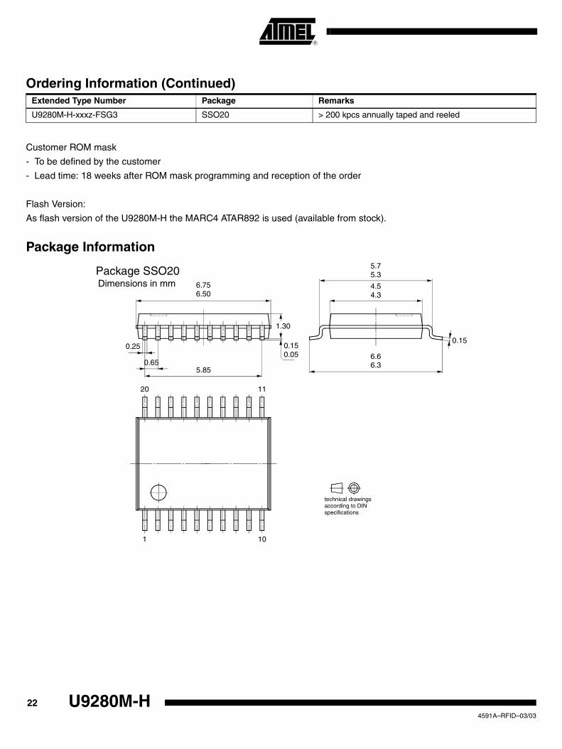
Package Information
Ordering Information (Continued)Extended Type Number Package Remarks
U9280M-H-xxxz-FSG3 SSO20 > 200 kpcs annually taped and reeled
technical drawingsaccording to DINspecifications
Package SSO20Dimensions in mm 6.75
6.50
0.25
0.655.85
1.30
0.150.05
5.75.3
4.54.3
6.66.3
0.15
20 11
1 10
22 U9280M-H 4591A–RFID–03/03

Printed on recycled paper.
© Atmel Corporation 2003.Atmel Corporation makes no warranty for the use of its products, other than those expressly contained in the Company’s standard warrantywhich is detailed in Atmel’s Terms and Conditions located on the Company’s web site. The Company assumes no responsibility for any errorswhich may appear in this document, reserves the right to change devices or specifications detailed herein at any time without notice, and doesnot make any commitment to update the information contained herein. No licenses to patents or other intellectual property of Atmel are grantedby the Company in connection with the sale of Atmel products, expressly or by implication. Atmel’s products are not authorized for use as criticalcomponents in life support devices or systems.
Atmel Headquarters Atmel Operations
Corporate Headquarters2325 Orchard ParkwaySan Jose, CA 95131TEL 1(408) 441-0311FAX 1(408) 487-2600
EuropeAtmel SarlRoute des Arsenaux 41Case Postale 80CH-1705 FribourgSwitzerlandTEL (41) 26-426-5555FAX (41) 26-426-5500
AsiaRoom 1219Chinachem Golden Plaza77 Mody Road TsimhatsuiEast KowloonHong KongTEL (852) 2721-9778FAX (852) 2722-1369
Japan9F, Tonetsu Shinkawa Bldg.1-24-8 ShinkawaChuo-ku, Tokyo 104-0033JapanTEL (81) 3-3523-3551FAX (81) 3-3523-7581
Memory2325 Orchard ParkwaySan Jose, CA 95131TEL 1(408) 441-0311FAX 1(408) 436-4314
Microcontrollers2325 Orchard ParkwaySan Jose, CA 95131TEL 1(408) 441-0311FAX 1(408) 436-4314
La ChantrerieBP 7060244306 Nantes Cedex 3, FranceTEL (33) 2-40-18-18-18FAX (33) 2-40-18-19-60
ASIC/ASSP/Smart CardsZone Industrielle13106 Rousset Cedex, FranceTEL (33) 4-42-53-60-00FAX (33) 4-42-53-60-01
1150 East Cheyenne Mtn. Blvd.Colorado Springs, CO 80906TEL 1(719) 576-3300FAX 1(719) 540-1759
Scottish Enterprise Technology ParkMaxwell BuildingEast Kilbride G75 0QR, Scotland TEL (44) 1355-803-000FAX (44) 1355-242-743
RF/AutomotiveTheresienstrasse 2Postfach 353574025 Heilbronn, GermanyTEL (49) 71-31-67-0FAX (49) 71-31-67-2340
1150 East Cheyenne Mtn. Blvd.Colorado Springs, CO 80906TEL 1(719) 576-3300FAX 1(719) 540-1759
Biometrics/Imaging/Hi-Rel MPU/High Speed Converters/RF Datacom
Avenue de RochepleineBP 12338521 Saint-Egreve Cedex, FranceTEL (33) 4-76-58-30-00FAX (33) 4-76-58-34-80
Web Sitehttp://www.atmel.com
4591A–RFID–03/03 xM
Atmel® is the registered trademark of Atmel.
Other terms and product names may be the trademarks of others.

This datasheet has been download from:
www.datasheetcatalog.com
Datasheets for electronics components.


