Embed Size (px)
Citation preview
ICEM Modelling of Microcontroller Current
Activity
Jean-Luc Levant a,∗, , Mohamed Ramdani b and
Richard Perdriau b
aATMEL - La Chantrerie - Route de Gachet - 44000 Nantes - France
bESEO - 4, rue Merlet-de-la-Boulaye - BP 926 - 49009 Angers Cedex 01 - France
Abstract
Better prediction of electromagnetic compatibility (EMC) for components is be-coming a topical demand, due to technology improvements. It is requested by inte-grated circuit (IC) manufacturers as well as by equipment integrators. The FrenchUTE standardisation group has proposed an EMC modelling methodology for ICs,called ICEM (Integrated Circuit Electromagnetic Model). This proposal improvesand extends the IBIS standard towards conducted emission prediction (and later ra-diated emission) by providing additional information modelling the power networkand the dynamic current activity of an IC, thus allowing the chip manufacturerto justify the package used as well as the number of power supply pins, and theequipment manufacturer to tune power supply and decoupling networks.
After a brief introduction to the ICEM model and the associated methods, thisarticle shows a way of obtaining dynamic current activity models by measuring thecurrent consumed on the IC power supply pins. The use of ICEM for the optimisationof decoupling networks, the evaluation of power supply noise and the tuning of thesurface of power and ground planes is presented for the first time with subsequentresults.
Key words: Electromagnetic compatibility, ICEM, measurement, modelling,simulation
∗ Corresponding author. Tel. (33/0) 2 40 18 18 77Email address: [email protected] (Jean-Luc Levant).
Preprint submitted to Elsevier Science 24 March 2005
1 Introduction
According to the MEDEA+ EDA roadmap [5], despite ever decreasing sup-ply voltages (0.3 V in 2013), conducted emission levels of integrated circuitsshould slightly increase (100 µV in 2013, with 25 GHz system clock, insteadof 90). Therefore, predicting conducted-mode emission is an ever growind de-mand for future generation circuits.This prediction relies on the knowledge of the current flowing in the powersupply networks of an IC and its PCB. In order to obtain this current, thebehaviour of the power supply network impedance and the profile of the in-stantaneous current consumed by the chip core both have to be identified.Each building block of the IC architecture (core, memories, buffers, analoguefunctions) can be modelled this way. ICEM [4] proposes a methodology ded-icated to obtaining these models; they can be elaborated either within thedesign phase or from measurements on the working silicon.Figure 1 depicts the main principles of ICEM modelling in the case of a mi-crocontroller, including core and buffers.The core and buffer models include the power supply impedance as well asa specific current activity (RESET mode, memory accesses ...). An isolationresistance between both grounds represents the substrate leakage resistanceand is supplied by the model as well. Of course, depending of the IC, eachentity can have its own ICEM model.The ICEM methodology can be used either within the IC design phase or withmeasurements on an existing chip; both approaches are displayed in figure 2.Only the measurement-based approach is introduced in this article : the trans-fer function of the power supply network is characterized in frequency domainfrom measurements, then it is coupled with time-domain measurements of theexternal current, in order to obtain a time-domain representation of the in-ternal current. In addition to that, a methodology to compute the predictedexternal current from the simulated internal one is under development andvalidation [3].
2 Obtaining the ICEM model from measurements
This approach consists in modelling the power supply network and the dy-namic current for a given activity. This article introduces an original method-ology for both modelling steps. An 8-bit microcontroller from the 80C51 familyis chosen as a demonstrator.
2
2.1 Power supply model of the microcontroller
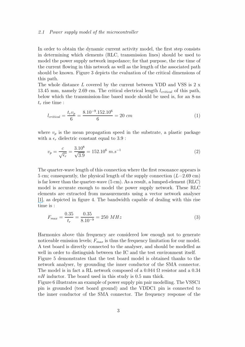
In order to obtain the dynamic current activity model, the first step consistsin determining which elements (RLC, transmission lines) should be used tomodel the power supply network impedance; for that purpose, the rise time ofthe current flowing in this network as well as the length of the associated pathshould be known. Figure 3 depicts the evaluation of the critical dimensions ofthis path.The whole distance L covered by the current between VDD and VSS is 2 x13.45 mm, namely 2.69 cm. The critical electrical length lcritical of this path,below which the transmission-line based mode should be used is, for an 8-nstr rise time :
lcritical =trvp
6=
8.10−9.152.106
6= 20 cm (1)
where vp is the mean propagation speed in the substrate, a plastic packagewith a ǫr dielectric constant equal to 3.9 :
vp =c
√ǫr
=3.108
√3.9
= 152.106 m.s−1 (2)
The quarter-wave length of this connection where the first resonance appears is5 cm; consequently, the physical length of the supply connection (L=2.69 cm)is far lower than the quarter-wave (5 cm). As a result, a lumped-element (RLC)model is accurate enough to model the power supply network. These RLCelements are extracted from measurements using a vector network analyser[1], as depicted in figure 4. The bandwidth capable of dealing with this risetime is :
Fmax =0.35
tr=
0.35
8.10−9= 250 MHz (3)
Harmonics above this frequency are considered low enough not to generatenoticeable emission levels; Fmax is thus the frequency limitation for our model.A test board is directly connected to the analyser, and should be modelled aswell in order to distinguish between the IC and the test environment itself.Figure 5 demonstrates that the test board model is obtained thanks to thenetwork analyser, by grounding the inner conductor of the SMA connector.The model is in fact a RL network composed of a 0.044 Ω resistor and a 0.34nH inductor. The board used in this study is 0.5 mm thick.Figure 6 illustrates an example of power supply pin pair modelling. The VSSC1pin is grounded (test board ground) and the VDDC1 pin is connected tothe inner conductor of the SMA connector. The frequency response of the
3
impedance up to 300 MHz can be divided into three parts. Under 10 MHz, theimpedance is capacitive and its value can be computed at a given frequency.At 15 MHz, it becomes resistive and its value is read on the plot. Above 20MHz and until 300 MHz, the impedance is inductive and can be computed aswell at another given frequency. Figure 7 represents the partial model of thepower supply network for this pair.The same methodology is used for every power supply pair (core and buffers).
2.2 Current activity model of the integrated circuit
The modelling methodology relies on the measurement of the external currentconsumed by the IC [2]; figure 8 shows the measurement and acquisition chain.This measurement is achieved by inserting a resistor (Rm) in the power supplyrail and plugging a differential probe across it; Rm must be low enough togenerate only a small supply voltage drop (<100 mV). In this example, threedifferential probes help rebuilding the external current (Iext); then the scopedirectly performs the addition of the three measurements. The results aresaved in text format, usable by the processing algorithm written in Matlab.In order to obtain the consumed current model, a given activity must bedefined; in this example, the RESET mode of the microcontroller is chosen.The general principle relies on the knowledge of the power supply network aswell as of the measurement of the external current consumed by this network,as depicted in figure 9. The equivalent Iint current flows into two parallelbranches; measuring Iext leads to Iint by determining the transfer functionKz(f) :
Iint = Iext.Kz(f) where Kz(f) =Rm + Z1 + Z2
Z2
(4)
In order to achieve this principle, the time-domain current Iext(t) must beconverted into the frequency domain Iext(f) thanks to a FFT. Then the prod-uct Kz(f).Iext(f) yields the internal current Iint(f). An inverse FFT convertsIint(f) back into the time domain Iint(t). The methodology is explained infigure 10.In order to preserve model accuracy, appropriate time and frequency resolu-tions for the measurements must be correctly defined. Internal currents canbe observed during several microseconds (which depends from the chosen ac-tivity) while having transitions times as low as 1 ns.These criteria define the electrical characteristics of the scope dedicated toIext(t) acquisition. Modelling the activity in RESET mode requires a 4 µsacquisition time, a 100 ps time resolution (10 points in each transition) and,consequently, a 40 Kbyte trace depth. The acquisition chain is composed of1.7 GHz differential probes and a 4 GHz oscilloscope. The whole bandwidth
4
is thus :
Btot(GHz) =
√
1
1.72+
1
42= 1.56 GHz (5)
The sampling frequency of the scope is 10 GHz : easily high enough to as-sure accurate measurements. Moreover, it is mandatory to check out thatsampling-induced noise does not affect measurements; should it be the case,an anti-aliasing filter must be included in the acquisition chain. Lowpass filtersintegrated in some oscilloscopes enable to fit their bandwidth to the observedsignal.Figure 11 displays both the measured current Iext(t) and the internal currentIint(t) extracted thanks to this method. The internal current flowing into theIC is much higher than the external one (150 mA versus 7 mA peaks); thepower supply network is responsible for filtering.Figure 12 shows a significant correlation between the external current regen-erated by the FFT/IFFT method and the measured one.
3 ICEM model use
3.1 Noise estimation on power supplies
The full ICEM model of the IC is depicted in figure 13. The core as well as thebuffers are modelled along with the test board (SMA connector and PCB).IintC and IintB represent the current activity models in RESET mode.The power supply model and the current profile enable the measurement ofthe supply noise (on VDDC). Figure 14 shows a good correlation between thesimulated noise and the measured one; the model should be improved in orderto refine the prediction.
3.2 Decoupling network optimisation
Another possible use is the optimisation of the decoupling network. As an ex-ample, four decoupling capacitors were added to the previous model in orderto lower the impedance of the power supply network in the frequency bandof interest. Figure 15 demonstrates an excellent correlation between the sim-ulated network and the measured one.Of course, the model of the decoupling capacitors must be determined; sub-sequent information is often provided in data books. In our case, the modelswere measured with the network analyser, in order to state the limits of the
5
ICEM approach. The results prove that accurate modelling easily providesenough accuracy to meet the goals of EMC analysis : in this example, it canbe noticed that the 10 nF capacitor has hardly any influence and could thenbe omitted.
3.3 Influence of ground and power planes
The ICEM model could be used as well for evaluating and optimising the sur-faces of ground and power planes. They act as efficient decoupling capacitorsin high frequency due to their low ESR and inductances. Figure 16 shows theirinfluence on the impedance profile.The decoupling capacitance associated to ground and power planed dependson surface, thickness and dielectric. Its value is given by the following formula:
C = 8.85 ǫr
A
d(pF ) (6)
where ǫr is the dielectric constant (4.9 for FR4 epoxy), A the surface (m2)and d the distance (m) between both planes. For a 25 cm2 wide, 0.5 mmthick plane, the capacitance reaches 217 pF. Figure 16 shows that both planescompensate for network antiresonance around 400 MHz.
4 Conclusion
The ICEM methodology relies on the description of two submodels : the powersupply network and the dynamic current bound to a specific activity. This ar-ticle shows that accurate modelling of the network and the internal current ismade possible without too many complications. In addition to that, it provesthat both models are accurate enough to evaluate noise levels of power sup-plies, to optimise the decoupling networks (number and values of capacitors)as well as to predict the surface of copper planes up to 300 MHz. Anotheruse, which is not considered here and is bound to more accurate knowledge ofthe current flowing on the board, is the prediction of conducted and radiatedemission levels of the IC and its associated PCB. The ICEM model is beingcurrently validated in these application fields, and the first results are reallyencouraging. Furthermore, new models, based on transmission lines, are beingstudied for UHF frequency bands above 300 MHz; promising results shouldbe eventually published.
6
References
[1] J.L. Levant, M. Ramdani, and R. Perdriau. Power supply network modeling. InEMC Compo 2002, pages 75–78, November 2002.
[2] J.L. Levant, M. Ramdani, and R. Perdriau. ICEM modeling of microcontrollercurrent activity. In EMC Compo 2002, pages 88–91, November 2002.
[3] R. Perdriau, M. Ramdani, J.L. Levant, E. Tinlot, and Anne-Marie Trullemans-Anckaert. An EMC-oriented VHDL-AMS simulation methodology for dynamiccurrent activity assessment. Microelectronics Journal, Special Section on EMCCOMPO 2002, 2003.
[4] IEC EMC Task Force. IEC62014-3 : Integrated circuit electromagneticmodel. Draft technical report, IEC, November 2001. http://intrage.insa-tlse.fr/∼etienne/Emc/icemcdv.PDF.
[5] MEDEA+ EDA roadmap. System design with respect to EMC.http://intrage.insa-tlse.fr/∼etienne/Emc/emcroadmap.htm.
7
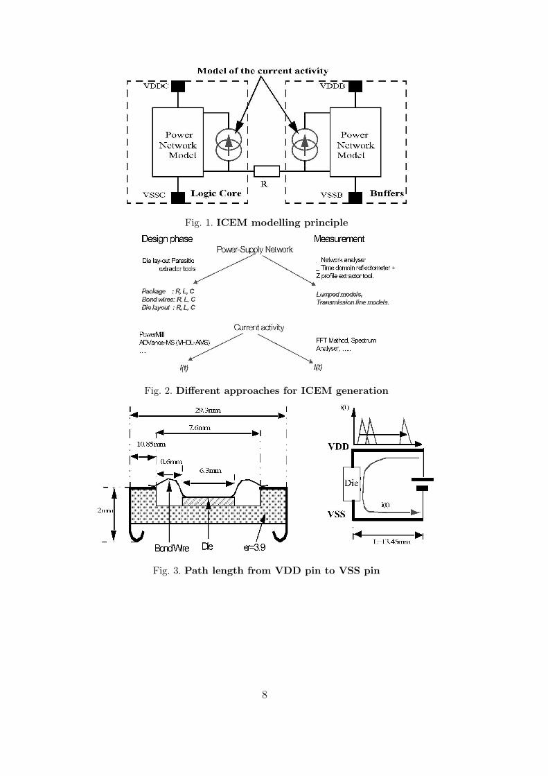
Fig. 1. ICEM modelling principle
Fig. 2. Different approaches for ICEM generation
Fig. 3. Path length from VDD pin to VSS pin
8
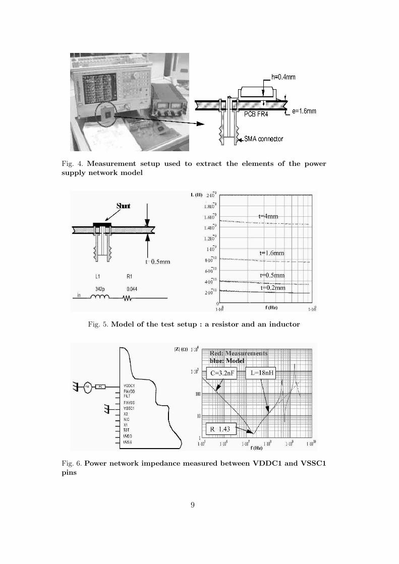
Fig. 4. Measurement setup used to extract the elements of the powersupply network model
Fig. 5. Model of the test setup : a resistor and an inductor
Fig. 6. Power network impedance measured between VDDC1 and VSSC1pins
9
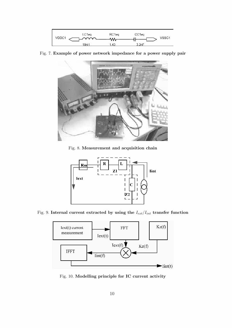
Fig. 7. Example of power network impedance for a power supply pair
Fig. 8. Measurement and acquisition chain
Fig. 9. Internal current extracted by using the Iext/Iint transfer function
Fig. 10. Modelling principle for IC current activity
10
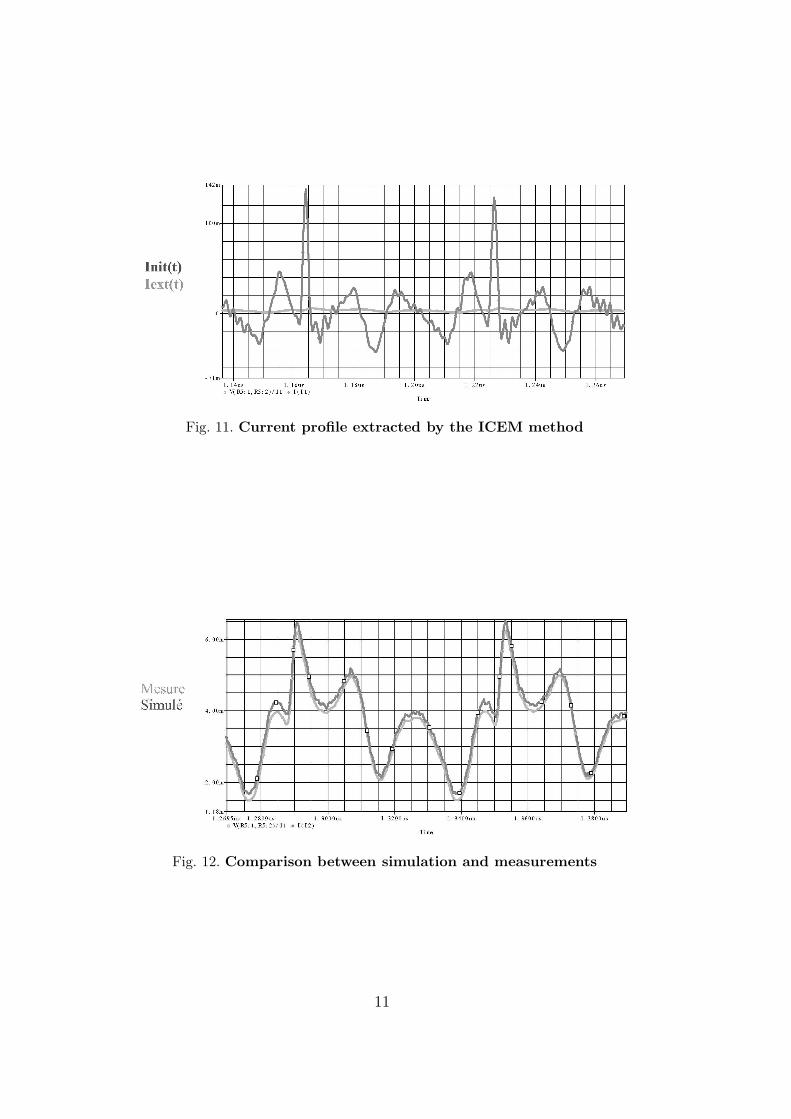
Fig. 11. Current profile extracted by the ICEM method
Fig. 12. Comparison between simulation and measurements
11
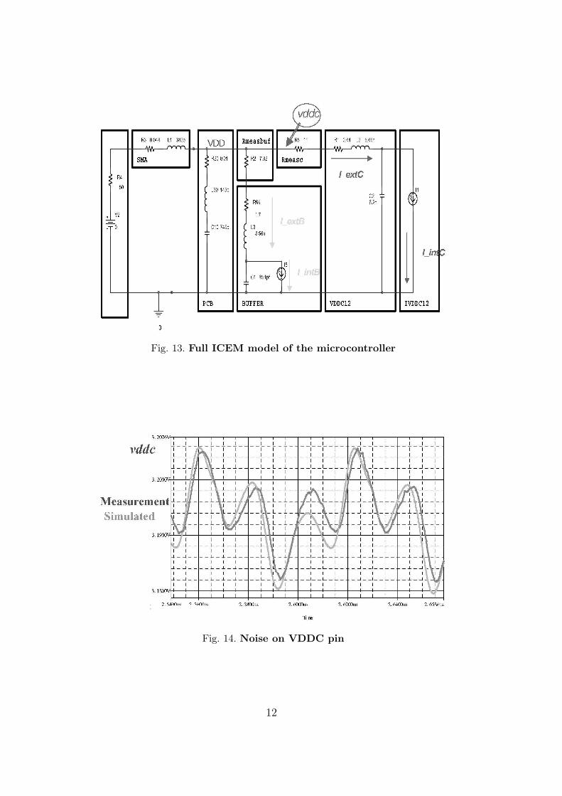
Fig. 13. Full ICEM model of the microcontroller
Fig. 14. Noise on VDDC pin
12
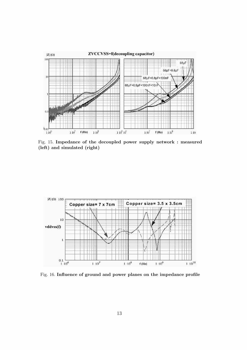
Fig. 15. Impedance of the decoupled power supply network : measured(left) and simulated (right)
Fig. 16. Influence of ground and power planes on the impedance profile
13


![[BAB I] Microcontroller ATMEGA8535](https://img.pdfslide.net/doc/110x75/635d9893a0f1eac29f0c45be/bab-i-microcontroller-atmega8535.jpg)


