Embed Size (px)
Citation preview

IEEE TRANSACTIONS ON POWER ELECTRONICS, VOL. 29, NO. 11, NOVEMBER 2014 6139
Modeling and Design of Voltage Support ControlSchemes for Three-Phase Inverters Operating Under
Unbalanced Grid ConditionsMiguel Castilla, Jaume Miret, Member, IEEE, Antonio Camacho, Luis Garcıa de Vicuna, and Jose Matas
Abstract—Three-phase inverters equipped with voltage supportcontrol schemes have been successfully used to alleviate the nega-tive impact of voltage imbalance on electric power systems. Withthese schemes, dc-link voltage ripple and current harmonics aresignificantly reduced by processing the positive and negative se-quence components separately. However, the design methods fortuning the parameters of these control schemes have one or moreof the following limitations: 1) the design is a very time-consumingtask, 2) it is conservative, 3) it does not guarantee the specificationsfor all the considered situations, and 4) the system can be unstablein some abnormal conditions. As an alternative, this paper presentsa design method based on the analysis of oscillations in nonlinearsystems. The method proceeds by first developing simple and ac-curate models of the power system, second it reveals the systemfeatures through an in deep analysis of the derived models, andthird it introduces a systematic design procedure for tuning theparameters of the control schemes. As an example, a voltage sup-port control scheme for a three-phase inverter operating under anunbalanced voltage sag is designed and validated experimentally.
Index Terms—Averaging, circuit modeling, control design,power conversion, voltage control.
I. INTRODUCTION
TRADITIONALLY switching power converters have beenpredominantly employed in domestic, industrial, and in-
formation technology applications. However, due to new ad-vances in power semiconductor and digital signal processortechnologies, the application of power converters in electricpower systems has recently gain considerably more attention.Thus, power converters are increasingly employed in power sys-tems for power conditioning [1]–[4], compensation [5]–[7], andfiltering [8]–[12].
In power systems, the voltage imbalance can cause severeproblems to energy sources, rotating equipments, and loads.The power production of energy sources reduces with grid volt-age imbalance due to the high ripple current placed in the dcbus [13], [14]. The presence of grid voltage imbalance degrades
Manuscript received July 17, 2013; revised September 15, 2013 andNovember 1, 2013; accepted December 21, 2013. Date of publication Jan-uary 2, 2014; date of current version July 8, 2014. This work was supported bythe Ministerio de Economıa y Competitividad of Spain under Project ENE2012-37667-C02-02. Recommended for publication by Associate Editor F. Wang.
The authors are with the Department of Electronic Engineering, Tech-nical University of Catalonia, 08800 Vilanova i la Geltru, Spain (e-mail:[email protected]; [email protected]; [email protected]; [email protected]; [email protected]).
Digital Object Identifier 10.1109/TPEL.2013.2296774
the lifespan of the rotating machinery due to the limited negativesequence capability [15]. Then, power converters equipped withvoltage support control schemes are employed to alleviate theseadverse effects [16]–[20]. In these schemes, a positive sequencevoltage loop is responsible to correct the voltage deviation, byinjecting the suitable positive sequence reactive power [16]. Byoperating in parallel, a negative sequence voltage loop attenu-ates the voltage imbalance through the provision of the neces-sary negative sequence reactive power [17], [18]. Therefore, thepower quality of the grid voltage is notably improved.
The design of these voltage control schemes for unbalancedpower systems has been usually carried out by case studies andsimulation tools [19], [20]. Therefore, a large number of ex-periments under different set of conditions were necessary toguarantee a proper operation for all the considered situations,which results in a very time-consuming task. Alternatively ap-proximate models of the system have been derived to design thecontrol schemes. These models are generally based on a powerbalance equation which does not take into account the completedynamics of the system [21]–[23]. Although some improvementof the approximate models can be found in the literature [24],the control design is in general conservative. Moreover, in cer-tain abnormal grid conditions, the system performance is poorand it can be even unstable [24].
This paper introduces a mathematical tool to design volt-age support control schemes for grid-connected power convert-ers. First, a modeling method based on the analysis of oscil-lations in nonlinear systems is used to model the power con-verter [25], [26]. This method extracts the low-frequency dy-namics of the power converter by separating the variables infast and slow time-varying signals and by averaging the result-ing models. A similar method was previously presented in [27]to model resonant power converters. In this paper, the method isrevised and adapted to the new scenario of grid-connected powerconverters. This revision includes the classification of the powerconverter variables and the derivation of the suitable averagedmodels. Second, an in-depth analysis of the power converter iscarried out by making use of the averaged models. The exactfeatures and the real performance of the power converter are re-vealed by the analysis, and a full and deep understanding of thesystem behavior is achieved by the identification of previouslyunknown characteristics. Third, a systematic design procedurefor tuning the parameters of the voltage control schemes is pre-sented. The closed-loop characteristics of the power convertersare given by fulfilling the typical frequency domain specifica-tions (i.e., control bandwidth and phase margin). Thanks to the
0885-8993 © 2013 IEEE. Personal use is permitted, but republication/redistribution requires IEEE permission.See http://www.ieee.org/publications standards/publications/rights/index.html for more information.

6140 IEEE TRANSACTIONS ON POWER ELECTRONICS, VOL. 29, NO. 11, NOVEMBER 2014
Fig. 1. Diagram of the grid-connected power converter.
method, good performance is ensured even during abnormalgrid conditions.
The rest of the paper is organized as follows. In Section II, thepower system is described and the averaging procedure is intro-duced. In Section III, the model of the complete power systemis derived, including the power converter, the voltage controlscheme, and the electrical grid. In Section IV, the particularfeatures of the power system are revealed through the analysisof the small-signal model. In Section V, the systematic designprocedure for tuning the parameters of the voltage control ispresented. In Section VI, the design method is validated by test-ing a low power experimental prototype during an unbalancedvoltage sag. Section VI is the conclusion of the paper.
II. SYSTEM DESCRIPTION AND MODELING APPROACH
This section describes the power system considered in thisstudy and presents the modeling approach used to analyze it.
A. Power System
Fig. 1 shows the diagram of the power system including thepower converter, the voltage control, and the electrical grid. Thepower converter is a three-phase three-wire voltage-source in-verter. The voltage control senses both the voltage at the pointof common coupling (PCC) and the output current of the powerconverter, and it generates the reference current for the internalcontrol loop of the power converter. The ac network is repre-sented as a series connection of the grid impedance and the acvoltage source.
The purpose of the voltage control is to regulate the voltageof the PCC. In normal operation, the amplitude of the volt-age v is regulated to the reference voltage Vref . In this study,the voltage control is designed to also cope with unbalancedgrid voltage. Thus, the injection of reactive power by positiveand negative sequences is necessary to accomplish the task ofvoltage regulation [19], [20].
The mathematical models developed in this study are basedon the stationary reference frame. The control schemes are alsoimplemented in this frame. Fig. 2 shows a diagram of the com-plete power system model. In this diagram, the voltage controlhas been divided into three main blocks: the sequence extractor,the voltage control loop, and the reference current generator.The sequence extractor is responsible for estimating the pos-itive and negative sequence components of the PCC voltage.The symmetrical components of the PCC voltage can be writtenin three-wire systems as sinusoidal signals rotating at the grid
frequency ω [20]
v+α = V + cos(ωt + ϕ+) (1)
v+β = V + sin(ωt + ϕ+) (2)
v−α = V − cos(−ωt − ϕ−) (3)
v−β = V − sin(−ωt − ϕ−). (4)
Note that, to simplify the study, the zero sequence voltagecomponents present in some fault conditions (for instance, insingle-line-to-ground faults with ac grid grounded) are not con-sidered. The outputs of the sequence extractor are also sinusoidalsignals but operating at the estimated grid frequency ωe
v+αe = V +
e cos(ωet + ϕ+e ) (5)
v+βe = V +
e sin(ωet + ϕ+e ) (6)
v−αe = V −
e cos(−ωet − ϕ−e ) (7)
v−βe = V −
e sin(−ωet − ϕ−e ). (8)
Note that the amplitudes of the variables defined in (1)–(8) aresupposed to be slowly varying functions of time. Precisely themain objective of the voltage loop is to regulate these slow vari-ables to the voltage references. The final purpose is to achieve,in steady state, the following results:
V + = V +ref (9)
V − = V −ref . (10)
To this end, the voltage loop provides the reference reactivepower necessary for the voltage regulation; see Fig. 2. The refer-ence generator determines the reference current for the internalcontrol loops. The outputs of the power converter and the elec-trical grid blocks depicted in Fig. 2 are the output currents andthe PCC voltages, respectively.
It is worth mentioning that only slow time-varying signalsare of interest for the analysis and design of the voltage controlloop. Below, a modeling approach for extracting the significantlow-frequency information of the power system is described.
B. Analysis of Oscillations in Nonlinear Systems
Several methods can be found in the literature for the study ofoscillations in nonlinear systems [25], [27]. In these methods,oscillating signals are identified as fast time-varying variables.Amplitudes of the oscillating signals are considered to be slowlytime-varying variables. A step-by-step procedure intended forthe derivation of averaged large-signal models of nonlinear sys-tems is presented below [27]. The method is adapted in thisstudy to the modeling of grid-connected power converters.
1) Write the power system model and derive its steady-statesolution (i.e., the fast variables).
2) Insert this solution into the system model. If the result-ing system is nonlinear, the nonlinear terms should be re-placed by their fundamental harmonic components (whichis known as harmonic linearization). At this point, themodel has been linearized in a large-signal sense, and it

CASTILLA et al.: MODELING AND DESIGN OF VOLTAGE SUPPORT CONTROL SCHEMES FOR THREE-PHASE INVERTERS 6141
Fig. 2. Diagram of the complete power system model including the power converter, the electrical grid, and the voltage control.
Fig. 3. Diagram of the averaged model of the power system.
can be written in a general form as
f1c(t) cos(ωt) + f1s(t) sin(ωt)
= f2c(t) cos(ωt) + f2s(t) sin(ωt). (11)
In (11), the sinusoidal signals are fast variables and the am-plitude of these signals are supposed to be slowly varyingfunctions of time.
3) The averaged large-signal model is derived by imposing aharmonic balance. That is,
f1c(t) = f2c(t) (12)
f1s(t) = f2s(t). (13)
The result is a model that describes the behavior of the slowvariables.
III. AVERAGED MODEL OF THE POWER SYSTEM
This section is devoted to the derivation of the averaged modelof the power system. A diagram of this model is shown in Fig. 3.
A. Averaged Model of the Grid and the Power Converter
From Fig. 1, the model of the electrical grid in stationaryreference frame can be written as
vα = vgα + Lgdiαdt
(14)
vβ = vgβ + Lgdiβdt
. (15)
For the design of the external control loop, the internal currentcontrol is assumed to be a perfect tracking loop and thereforethe output current is normally expressed as [17]
iα = i∗α (16)
iβ = i∗β . (17)
The reference currents can be separated in terms of active andreactive reference currents as
i∗α = i∗α,P + i∗α,Q (18)
i∗β = i∗β ,P + i∗β ,Q (19)
where
i∗α,P =23
v+αeP
(v+αe)2 + (v+
βe)2(20)
i∗β ,P =23
v+βeP
(v+αe)2 + (v+
βe)2(21)
i∗α,Q =23
[v+
βeQ+ref
(v+αe)2 + (v+
βe)2+
v−βeQ
−ref
(v−αe)2 + (v−
βe)2
](22)
i∗β ,Q =23
[−v+
αeQ+ref
(v+αe)2 + (v+
βe)2+
−v−αeQ
−ref
(v−αe)2 + (v−
βe)2
]. (23)
The active power P is transferred to the grid by the use of (20)and (21) [28]. The reactive power is injected via both positiveand negative sequences by making use of (22) and (23) [29].
The averaged model of the electrical grid and the power con-verter is derived using the modeling procedure described in theprevious section; see details on this derivation on Appendix I.The obtained model can be written as
V + = V +g +
23
ωeLgQ+ref
V +e
(24)
V − = V −g − 2
3ωeLgQ
−ref
V −e
. (25)
The support mechanism to the PCC voltage can be identifiedfrom (24) and (25). As usual in inductive networks, the effect ofthe active power is negligible and then P is not present in (24)and (25). The injection of reactive power via positive sequenceincreases the positive sequence voltage at the PCC. Besides theinjection of reactive power via negative sequence decreases thenegative sequence voltage at the PCC. The ability to reduce thevoltage deviations depends largely on the grid impedance andthe converter power rating (which, in fact, limits the maximumreactive power that can be injected into the electrical grid).
B. Averaged Model of the Sequence Extractor
Fig. 4 shows the diagram of the voltage sequence extrac-tor considered in this study [30], [32]. It consists of threemain blocks: a direct/quadrature voltage extractor, a frequency

6142 IEEE TRANSACTIONS ON POWER ELECTRONICS, VOL. 29, NO. 11, NOVEMBER 2014
Fig. 4. Diagram of the voltage sequence extractor.
estimator, and a sequence voltage calculator. The first block isused to extract the direct and quadrature components of the in-put signals. To this end, the extractor behaves as a band-passfilter for the direct signals and as a low-pass filter for the quadra-ture signals. The dynamic model of the extractor can be derivedfrom [28] and it can be written as
dvαde
dt= ωe [2ξ(vα − vαde) − vαqe ] (26)
dvαqe
dt= ωevαde +
vαqe
ωe
dωe
dt(27)
dvβde
dt= ωe [2ξ(vβ − vβde) − vβqe ] (28)
dvβqe
dt= ωevβde +
vβqe
ωe
dωe
dt(29)
being ξ the damping factor of the filters.In Fig. 4, the estimation of the grid frequency is employed
to online tune the direct and quadrature filters. Although sev-eral frequency estimators can be found in the literature, theimplementation presented in [31] is chosen here due to its highrobustness to amplitude variations in the grid voltage. The dy-namic model of the frequency estimator is
dωe
dt= −γωe
(vα − vαde)vαqe + (vβ − vβde)vβqe
(v+αe)2 + (v+
βe)2 + (v−αe)2 + (v−
βe)2(30)
where the parameter γ determines the speed of convergence.The sequence calculator block provides the positive and neg-
ative sequence components of the grid voltages [31]
v+αe =
vαde − vβqe
2(31)
v−αe =
vαde + vβqe
2(32)
v+βe =
vβde + vαqe
2(33)
v−βe =
vβde − vαqe
2. (34)
The averaged model of the sequence extractor is obtained byapplying the averaging procedure described in Section II. Thedetails on the model derivation can be found in Appendix I. The
Fig. 5. Diagram of the voltage support control loop.
model can be expressed as
dV +e
dt= ξωe(V + − V +
e ) +γ
2V +
e (V +V +e + V −V −
e )
(V +e )2 + (V −
e )2ω − ωe
ωe
(35)
dV −e
dt= ξωe(V − − V −
e ) +γ
2V −
e (V +V +e + V −V −
e )
(V +e )2 + (V −
e )2ω − ωe
ωe(36)
dωe
dt= γ
V +V +e + V −V −
e
(V +e )2 + (V −
e )2(ω − ωe). (37)
Note that the sequence extractor behaves as a third-ordernonlinear system. The complexity of the system is given by itslarge number of nonlinear terms and the coupling between theequations.
C. Averaged Model of the Voltage Control Loop
Fig. 5 shows the diagram of the voltage control loop analyzedin this study [32]. It is formed by three blocks: a grid voltage andimpedance estimator, a reference reactive power calculator, anda low-pass filter. The first block estimates the grid impedanceby using the method reported in [33]. Then, the grid voltage iscalculated as
V +ge =
√(v+
αe)2 + (v+βe)2 − 2
3ωeLgcQ
+ref√
(v+αe)2 + (v+
βe)2(38)
V −ge =
√(v−
αe)2 + (v−βe)2 +
23
ωeLgcQ−ref√
(v−αe)2 + (v−
βe)2(39)
where Lgc is a control parameter that in [32] was updated bythe online measure of the grid impedance. Note that (38) and(39) can be easily derived from the averaged model expressedin (24) and (25).
The second block calculates the reactive power under theassumption that the voltage at the PCC tracks accurately thereference voltage. In this case, the reactive power is written, bymaking use again of (24) and (25), as
Q+ =32
V +ref (V
+ref − V +
ge )ωeLgc
(40)
Q− =32
V −ref (V
−ge − V −
ref )ωeLgc
. (41)

CASTILLA et al.: MODELING AND DESIGN OF VOLTAGE SUPPORT CONTROL SCHEMES FOR THREE-PHASE INVERTERS 6143
The third block is a first-order low-pass filter that governs thetransient response of the reference reactive power
dQ+ref
dt= ωc(Q+ − Q+
ref ) (42)
dQ−ref
dt= ωc(Q− − Q−
ref ) (43)
where ωc is the filter cut-off frequency. This filter provides therequired time delay to ensure that the measures and previousestimations have reached the final values before they are usedto control the system.
The averaged model of the voltage control loop can be derivedby inserting (5)–(8) in (38) and (39), and then rearranging (40)–(43). The resulting model is written as
dQ+ref
dt= ωc
(Q+
ref
V +e
+32
V +ref
ωeLgc
)(V +
ref − V +e ) (44)
dQ−ref
dt= ωc
(Q−
ref
V −e
− 32
V −ref
ωeLgc
)(V −
ref − V −e ). (45)
D. Discussion on the Derived Averaged Models
As far as the authors know, there are no available models in theliterature that predict accurately the low-frequency dynamics ofthe sequence extractor introduced in [31] and the voltage controlloop recently presented in [32]. Thus, one of the contributions ofthis paper is the averaged models expressed in (35)–(37) for thesequence extractor and in (44)–(45) for the voltage control loop.Note that these models are essential to predict the features ofthe complete power system and to design the control parameters(i.e., ξ, γ, ωc , and Lgc ).
IV. SMALL-SIGNAL MODEL OF THE POWER SYSTEM
This section reveals the particular features of the voltagecontrol scheme considered in this study through the analysis ofthe small-signal model characteristics.
A. Small-Signal Model
The derivation of small-signal models is well documented inthe literature and then details on the model derivation will beomitted here. The definition of the involved variables is intro-duced in Appendix II. Fig. 6 shows the diagram of the small-signal models of the power system. Note that the positive- andnegative-sequence models are decoupled, which facilitates theanalysis of the system.
The transfer functions of the sequence extractor are derivedfrom (35)–(37), and they can be expressed as
G+se(s) =
ξωo
s + ξωo(46)
G−se(s) =
ξωo
s + ξωo(47)
ωe
ω(s) =
γ
s + γ. (48)
Fig. 6. Diagram of the small-signal model of the power system. (a) Positive-sequence model, (b) negative-sequence model.
The damping factor ξ governs the dynamics of the voltagesequence extractor and the parameter γ controls the dynamicsof the frequency estimator. From (46)–(48), the voltage andfrequency settling times can be expressed as
ts,v =5
ξωo(49)
ts,ω =5γ
. (50)
The transfer functions of the power system are derived from(24) and (25) and (46) and (47). They can be written as
G+ps(s) =
23
ωoLg
V +o
s + ξωo
s +(1 + 2
3ωo Lg Q+
o
(V +o )2
)ξωo
(51)
G−ps(s) = −2
3ωoLg
V −o
s + ξωo
s +(1 − 2
3ωo Lg Q−
o
(V −o )2
)ξωo
. (52)
Note that the poles of the transfer functions depend on thereactive power injection. As the injection increases, then thefrequency of the pole in (51) increases and in (52) decreases.With no injection, a zero-pole cancellation takes place and thepower plant is modeled as a variable gain. In fact, this gain relieson the grid frequency, the grid impedance, and the amplitude ofthe grid voltage.
Probably the most interesting result of this study is the transferfunctions of the voltage control loop. From (44) and (45), thesetransfer functions can be derived
G+v l(s) =
ωc
s
(Q+
o
V +o
+32
V +o
ωoLgc
)=
k+i
s(53)
G−v l(s) =
ωc
s
(Q−
o
V −o
− 32
V −o
ωoLgc
)=
k−i
s. (54)
Note that (53) and (54) are adaptive integral regulators. Theintegral gains change with the injection of reactive power andthe characteristics of the electrical grid (both amplitude and fre-quency). Besides two control design parameters ωc and Lgc areavailable to establish the preferred features for the closed-loop

6144 IEEE TRANSACTIONS ON POWER ELECTRONICS, VOL. 29, NO. 11, NOVEMBER 2014
system. What is even more important is that the integral regula-tors will eliminate the steady-state error in the sequence voltages(see the voltage loop blocks in Fig. 6) and thus the online es-timation of the grid impedance is no further required. In otherwords, the restriction Lgc=Lg is not really necessary for theproper operation of the control system. The main consequence isa simplification of the voltage control scheme presented in [32].
B. Closed-Loop Characteristics
The closed-loop characteristics, including system stabilityand transient response, can be evaluated by analyzing both theloop gain and the closed-loop transfer functions. From Fig. 6,these transfer functions can be written as
v+
v+ref
(s) =G+
ps(s)G+v l(s)
1 + T+(s)(55)
v−
v−ref
(s) =G−
ps(s)G−v l(s)
1 + T−(s)(56)
where
T+(s) = G+ps(s)G
+se(s)G
+v l(s) (57)
T−(s) = G−ps(s)G
−se(s)G
−v l(s). (58)
C. Discussion on the Derived Small-Signal Models
Another contribution of this paper is the small-signal modelsexpressed in (51) and (52) for the power converter and theelectrical grid and in (53) and (54) for the voltage control loop.As far as the authors know, there are no available models in theliterature that predict so accurately the small-signal dynamicsof these two subsystems. Note that these models provide insightabout the expected behavior of the complete system. In addition,they are essential to design the control parameters, as shown innext section.
V. DESIGN OF THE VOLTAGE CONTROL LOOP
This section presents a step-by-step procedure to calculatethe four design parameters of the voltage control scheme: ξ, γ,ωc , and Lgc . An example illustrates the application of the designprocedure.
A. Design Procedure
The settling time of a sequence extractor is usually betweenone and two periods of the grid voltage [30], [31]. By fixingthe settling time at one period of the grid voltage in (49) and(50), the control parameters of the sequence extractor can becalculated as
ξ =52π
(59)
γ =5ωo
2π. (60)
The control parameters of the voltage loop (ωc and Lgc )determine the values of the regulator integral gains, as shown in(53) and (54). Thus, ωc and Lgc will have a strong influence on
TABLE IPARAMETERS OF THE EXPERIMENTAL SETUP AND DESIGN SPECIFICATIONS
the magnitude of the loop gain transfer functions; see (57) and(58). However, the effect on the phase of these transfer functionsis negligible. Note that the poles and zeroes of the loop gaintransfer functions do not rely on the control parameters ωc andLgc . Taking in mind this fact, Lgc can be fixed to a known valueand then ωc could be chosen to accomplish the frequency domainspecifications for the control bandwidth and the phase margin.It is worth mentioning that the value of Lgc is established in thedesign process and it is not necessary to online measure the gridimpedance to update the value of this parameter. In this study,Lgc is set to the value of the grid impedance in the worst-casescenario (i.e., weak grid condition)
Lgc = Lg,w . (61)
With this choice, the accomplishment of the frequency do-main specifications is guaranteed for all the range of the gridimpedance, as shown below.
B. Design Example
A low-power experimental setup is used in the next sectionto validate the proposed design procedure. Here, the voltagecontrol scheme of this setup is designed. Table I lists the pa-rameters of the power system and the design specifications. Atype C voltage sag is used to evaluate the features of the system.The grid voltage components can be written as a function of thevoltage unbalance factor (VUF) as [34]
V +g =
11 + VUF
Vg (62)
V −g =
VUF1 + VUF
Vg (63)
where VUF = 0.3 is chosen in the experiments. The referencevoltages are selected in order to improve the PCC voltagesduring the sag. In particular, the positive-sequence voltage isincreased 6%, and the negative-sequence voltage is decreased
CASTILLA et al.: MODELING AND DESIGN OF VOLTAGE SUPPORT CONTROL SCHEMES FOR THREE-PHASE INVERTERS 6145
TABLE IISOLUTION TO THE DESIGN EXAMPLE
Fig. 7. Bode diagram of the loop gain T + (s) for the maximum and minimumgrid impedances.
TABLE IIICONTROL BANDWIDTH AND PHASE MARGIN AS A FUNCTION OF Lg
6%
V +ref = V +
o = 1.06V +g (64)
V −ref = V −
o = 0.94V −g . (65)
This is an arbitrary selection and other percentages arepossible by taking into account the limitations derived inAppendix III. The design is performed for weak grid conditionsand the corresponding reactive power symmetrical componentsfor this worst-case scenario are listed in Table I.
The solution to the design example is summarized in Table II.The design parameters ξ, γ, and Lgc are calculated from (59)–(61), respectively. The parameter ωc is determined by guaran-teeing a BW of 100 rad/s in the positive-sequence loop gain forLg=Lg,w . The reaching of this specification is verified by theBode diagram shown in Fig. 7. In addition, Table III lists themeasured control bandwidth and the phase margin for different
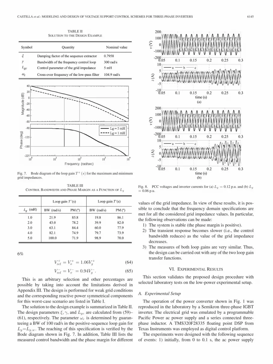
Fig. 8. PCC voltages and inverter currents for (a) Lg = 0.12 p.u. and (b) Lg
= 0.06 p.u.
values of the grid impedance. In view of these results, it is pos-sible to conclude that the frequency domain specifications aremet for all the considered grid impedance values. In particular,the following observations can be made:
1) The system is stable (the phase margin is positive).2) The transient response becomes slower (i.e., the control
bandwidth reduces) as the value of the grid impedancedecreases.
3) The measures of both loop gains are very similar. Thus,the design can be carried out with any of the two loop gaintransfer functions.
VI. EXPERIMENTAL RESULTS
This section validates the proposed design procedure withselected laboratory tests on the low-power experimental setup.
A. Experimental Setup
The operation of the power converter shown in Fig. 1 wasreproduced in the laboratory by a Semikron three-phase IGBTinverter. The electrical grid was emulated by a programmablePacific Power ac power supply and a series connected three-phase inductor. A TMS320F28335 floating point DSP fromTexas Instruments was employed as digital control platform.
The experiments were designed with the following sequenceof events: 1) initially, from 0 to 0.1 s, the ac power supply

6146 IEEE TRANSACTIONS ON POWER ELECTRONICS, VOL. 29, NO. 11, NOVEMBER 2014
Fig. 9. Positive and negative sequence components of the estimated voltage(in black) and reference voltage (in grey) for (a) Lg = 0.12 p.u. and (b) Lg =0.06 p.u.
emulates a normal grid condition; 2) from 0.1 to 0.6 s, a type Cvoltage sag with VUF = 0.3 was programmed in the ac powersupply; 3) the voltage control was intentionally inactive from0.1 to 0.2 s, in order to clearly show the PCC voltages duringthe abnormal grid condition; 4) from 0.2 to 0.6 s, the voltagecontrol was active and therefore the reactive power injectionand the PCC voltage regulation were put into operation. Thetransient response of the power converter was just evaluatedin this interval, once the voltage control scheme was activated.The power production of the system was maintained during thevoltage sag at P = 750 W; see Table I.
B. Tests for Weak Grid Conditions
Figs. 8–10 show the main waveforms of the power systemduring the sequence of events described above. In particular,the results of the tests for weak grid conditions are shown inpart (a) of these figures, while part (b) shows the results fora lower grid impedance. Note that the PCC voltages becomeunbalanced and their amplitudes are reduced during the volt-age sag; see Fig. 8(a). This loss of voltage quality can also beobserved in the reduction of positive sequence voltage and theincrease of negative sequence voltage; see Fig. 9(a). The reac-tive power injection activates the voltage regulation mechanismand places the symmetrical components of the PCC voltage attheir reference values with no steady-state error. The inverter
Fig. 10. Positive and negative sequence components of the reference reactivepower for (a) Lg = 0.12 p.u. and (b) Lg = 0.06 p.u.
TABLE IVCONTROL BANDWIDTH AND PHASE MARGIN AS A FUNCTION OF ωc
current can be seen in Fig. 8(a). In normal condition, only activecurrent is injected to the grid. During the sag, a current increaseis noticed, especially when the voltage control is activated. Notethat, in this case, the current is unbalanced due to the presenceof positive and negative sequence components. Thanks to thisunbalanced current both positive and negative sequence volt-ages can be regulated to their reference voltages. With balancedcurrent, only one of the voltage sequences could be controlledand then the control objectives expressed in (9) and (10) can-not be meet simultaneously. Probably the best waveforms toevaluate the transient response are the reference reactive power

CASTILLA et al.: MODELING AND DESIGN OF VOLTAGE SUPPORT CONTROL SCHEMES FOR THREE-PHASE INVERTERS 6147
Fig. 11. Reference reactive power Q+ref for several values of the control bandwidth. (a) 300 rad/s, (b) 200 rad/s, (c) 150 rad/s, (d) 100 rad/s, (e) 75 rad/s,
(f) 50 rad/s, (g) 30 rad/s, (h) 20 rad/s, and (i) 15 rad/s.
components. Fig. 10(a) shows a fast transient response with asettling time of 22.5 ms. This value is in good agreement withthe theoretical result (28.3 ms) derived by the analysis of (55).
C. Tests Using a Different Grid Impedance
The next experiment was performed to evaluate the effect ofusing a different impedance in the experimental setup. In par-ticular, a 2.5 mH (0.06 p.u.) inductor was used to emulate thegrid impedance. The parameters of the voltage control listedin Table II were maintained during the test (i.e., the controldesign was not updated for the new impedance). Also the refer-ence voltages listed in Table I were maintained to facilitate thecomparison between the two experiments.
Figs. 8(a)–10(b) show the results. Note that a higher currentand reactive power are necessary in this case to achieve thesame reference voltages. What is even more interesting is thatno steady-state error is noticed in the symmetrical componentsof the PCC voltage, see Fig. 9(b). This fact confirms that 1)the voltage control scheme behaves as an integral regulator, and2) the online measurement of the grid impedance is not reallynecessary to regulate the PCC voltage. The transient responseof the power system is slower in this case in comparison withthe results shown in Fig. 8(a)–10(a). The measured settling timeof the reference reactive power components is 80.9 ms; seeFig. 10(b). This result is in good agreement with the theoreticalvalue (82.1 ms) predicted by (55).
The measured results show a small ripple caused mainly bythe practical errors associated with the digital implementationof the control scheme (i.e., coefficient mismatch, quantization,delay). The magnitude of this ripple is reduced by decreasingthe value of Lg , as shown in Figs. 9 and 10. This valuable effectis due to the reduction of the control system bandwidth for
smaller values of Lg (see Table III). Thus, the filtering actionof the closed-loop system improves for lower values of the gridimpedance.
D. Tests Using Different Values of ωc
The last experiment evaluates the effect of using different val-ues for ωc . Table IV lists the control bandwidth and the phasemargin for a broad range of ωc values. Fig. 11 shows the transientresponse of the reference reactive power for the considered val-ues of ωc . Note that for high values, the transient response is veryfast. However, the capacity to reject low-frequency harmonicsis low and the start-up overshoot is high. These harmonics causeunwanted ripple in the reference signals, as shown in Fig. 11(a).Quite the opposite, a high harmonic rejection is reached and noovershoot is noticed for low values of ωc , as shown in Fig. 11(i).In this case, the main limitation is a slow transient response. Inview of the results, it seems obvious that a good solution forthe design tradeoff is to set the control bandwidth BW at 1/3of the bandwidth of the sequence extractor ξωo , as proposed inSection V.
VII. CONCLUSION
A theoretical methodology formulated for the analysis of theexternal control loops of three-phase grid-connected convert-ers has been presented in this paper. The method proceeds asfollows. First, the large-signal averaged models of the powersystem are developed by using a simple method to analyze os-cillations in nonlinear systems. Second, the system features arederived by making use of the linear analysis techniques based onsmall-signal models. Third, a control design method can be es-tablished with the system knowledge gained by the small-signal

6148 IEEE TRANSACTIONS ON POWER ELECTRONICS, VOL. 29, NO. 11, NOVEMBER 2014
analysis. In addition to the proposed design methodology, othermajor contributions of this study are as follows.
1) The averaged models for both the sequence extractor in-troduced in [31] and the voltage support control schemepresented in [32].
2) The small-signal models for the power system (includingthe power converter and the electrical grid) and the voltagesupport control scheme presented in [32].
With these models, the exact features and the real perfor-mance of the analyzed power system were revealed. The featurescan be summarized as follows.
1) The power system is stable for all the considered range ofoperation.
2) The transient response strongly depends on the value ofthe grid impedance.
3) The voltage control scheme behaves as a nonlinear integralregulator.
4) The online measurement of the grid impedance is notreally necessary for the correct operation of the system.
The application of the proposed methodology can be eas-ily extended to other power converters connected to the utilitygrid. It could be also employed to devise new control schemesand strategies with improved performance. In particular, severalcontrol strategies to determine the reference voltage values inaccordance with the grid characteristics (impedance, VUF, etc.)could be developed with the proposed averaged models. Theseideas are actually open for further research.
APPENDIX I
This appendix gives the detailed derivation of the averagedmodels of the power system and the voltage sequence extractor.
A. Averaged Model of the Power System
The steady-state voltages of the power system are defined by(1)–(8) and
v+gα = V +
g cos(ωt + ϕ+) (A1)
v+gβ = V +
g sin(ωt + ϕ+) (A2)
v−gα = V −
g cos(−ωt − ϕ−) (A3)
v−gβ = V −
g sin(−ωt − ϕ−). (A4)
The method proceeds next by inserting this solution in themodel (14) and (15) with the help of (16) and (23). The resultingmodel has the general form written in (11). By applying theharmonic balance (12) and (13) to this model, the averagedmodel expressed in (24) and (25) is obtained after some simplemanipulations.
B. Averaged Model of the Sequence Extractor
The steady-state solution (1)–(8) is first inserted in the model(26)–(34). The resulting model has the form expressed in (11).By using the harmonic balance (12) and (13), the averagedmodel (35)–(37) is derived.
APPENDIX II
This section defines the small-signal variables used in thisstudy. To this end, the averaged variables are decomposed insteady-state quantities and small signal variables
V + = V +o + v+ (A5)
V +e = V +
o + v+e (A6)
V +ref = V +
o + v+ref (A7)
V − = V −o + v− (A8)
V −e = V −
o + v−e (A9)
V −ref = V −
o + v−ref (A10)
ω = ωo + ω (A11)
ωe = ωo + ωe (A12)
Q+ref = Q+
o + q+ref (A13)
Q−ref = Q−
o + q−ref (A14)
where the subscript o denotes steady-state quantities and thesuperscript ˆ identifies the small-signal variables. Note that thesteady-state quantities of all the positive-sequence voltages havethe same value. This can be deduced by calculating the steady-state solution of (35) and (44). The same is true for all thenegative-sequence voltages in steady state. This fact can bedemonstrated by solving (36) and (45) in steady state. Also thesteady-state values of the grid frequency and the estimated gridfrequency coincide, as it can be confirmed from (37).
APPENDIX III
This appendix derives the theoretical limits to the voltagesupport control analyzed in this paper. The steady-state valuesof the positive and negative sequence voltages at the PCC canbe calculated by inserting the steady-state quantities from (A5),(A6), (A8), (A9) in (24) and (25)
V +o =
12
(V +
g +
√(V +
g
)2 +83ωoLgQ
+o
)(A15)
V −o =
12
(V −
g +
√(V −
g
)2 − 83ωoLgQ−
o
). (A16)
The maximum capability to compensate the negative se-quence voltage by the injection of negative sequence reactivepower is derived, from (A16), as
V −o min =
V −g
2(A17)
Q−o max =
38
(V −
g
)2
ωoLg. (A18)
The limits for the positive sequence reactive power are onlydictated by the converter power rating given that no additionallimits are introduced from (A15).
The theoretical limits have been verified by simulation re-sults, as shown in Fig. 12. The sequence of events used in the

CASTILLA et al.: MODELING AND DESIGN OF VOLTAGE SUPPORT CONTROL SCHEMES FOR THREE-PHASE INVERTERS 6149
Fig. 12. Normalized negative sequence voltage V −e /V −
g for several values of the negative sequence reactive power ratio Q−o /Q−
o m ax . (a) 0.2, (b) 0.4, (c) 0.6,(d) 0.8, (e) 1.0, and (f) 1.01.
experiments described in Section VI is repeated here to validatethe expressions (A17) and (A18). The voltage control is acti-vated at 0.2 s and, after a settling time, the negative sequencevoltage V −
e reaches the steady-state value V −o . Note that the
negative sequence voltage V −o reduces as the reactive power
Q−o increases. In particular, the minimum value for this voltage
is obtained when the reactive power is maximum, as shown inFig. 12(e). For higher values of the reactive power, (A16) hasno real solution and the system becomes unstable, as shown inFig. 12(f) for the case Q−
o = 1.01·Q−o max .
REFERENCES
[1] J. Rocabert, A. Luna, F. Blaabjerg, and P. Rodriguez, “Control of powerconverters in AC microgrids,” IEEE Trans. Power Electron., vol. 27,no. 11, pp. 4734–4749, Nov. 2012.
[2] J. M. Bloemink and T. C. Green, “Benefits of distribution-level powerelectronics for supporting distributed generation growth,” IEEE Trans.Power Del., vol. 28, no. 2, pp. 911–919, Apr. 2013.
[3] P. Nuutinen, P. Peltoniemi, and P. Silventoinen, “Short-circuit protectionin a converted-fed low-voltage distribution network,” IEEE Trans. PowerElectron., vol. 28, no. 4, pp. 1587–1597, Apr. 2013.
[4] E. Jamshidpour, B. Nahid-Mobarakeh, P. Poure, S. Pierfederici, andS. Saadate, “Distributed active resonance suppression in hybrid DC powersystems under unbalanced load conditions,” IEEE Trans. Power Electron.,vol. 28, no. 4, pp. 1833–1842, Apr. 2013.
[5] S.-C. Tan, C. K. Lee, and S. Y. Hui, “General steady-state analysis andcontrol principle of electric springs with active and reactive power com-pensations,” IEEE Trans. Power Electron., vol. 28, no. 8, pp. 3958–3969,Aug. 2013.
[6] H. Zhou, Y. Li, N. Zargari, Z. Cheng, R. Ni, and Y. Zhang, “Selec-tive harmonic compensation (SHC) PWM for grid-interfacing high-powerconverters,” IEEE Trans. Power Electron., vol. 29, no. 3, pp. 1118–1127,Mar. 2014.
[7] K. Alawasa, Abdel-Rady I. Mohamed, and W. Xu, “Active mitigationof subsynchronous interactions between voltage-source converters andpower networks,” IEEE Trans. Power Electron., vol. 29, no. 1, pp. 121–134, Jan. 2014.
[8] X. Sun, J. Zeng, and Z. Chen, “Site selection strategy of single-frequencytuned R-APF for background harmonic voltage damping in power sys-tems,” IEEE Trans. Power Electron., vol. 28, no. 1, pp. 135–143, Jan.2013.
[9] W.-H. Choi, C.-S. Lam, M.-C. Wong, and Y.-D. Han, “Analysis of DC-link voltage controls in three-phase four-wire hybrid active power filters,”IEEE Trans. Power Electron., vol. 28, no. 5, pp. 2180–2191, May 2013.
[10] N. Bottrell, M. Prodanovic, and T. C. Green, “Dynamic stability of amicrogrid with an active load,” IEEE Trans. Power Electron., vol. 28,no. 11, pp. 5107–5119, Nov. 2013.
[11] J. He, Y. W. Li, F. Blaabjerg, and X. Wang, “Active harmonic filteringusing current-controlled, grid-connected DG units with closed-loop powercontrol,” IEEE Trans. Power Electron., vol. 29, no. 2, pp. 642–653, Feb.2014.
[12] P. Acuna, L. Moran, M. Rivera, J. Dixon, and J. Rodriguez, “Improvedactive power filter performance for renewable power generation systems,”IEEE Trans. Power Electron., vol. 29, no. 2, pp. 687–694, Feb. 2014.
[13] A. J. Roscoe, S. J. Finney, and G. M. Burt, “Tradeoffs between AC powerquality and DC bus ripple for 3-phase 3-wire inverter-connected deviceswithin microgrids,” IEEE Trans. Power Electron., vol. 26, no. 3, pp. 674–688, Mar. 2011.
[14] L. Xiao, S. Huang, and K. Lu, “DC-bus voltage control of grid-connectedvoltage source converter by using space vector modulated direct powercontrol under unbalanced network conditions,” IET Power Electron, vol. 6,no. 5, pp. 925–934, May 2013.
[15] I. Jeong, B. J. Hyon, and K. Nam, “Dynamic modeling and control forSPMSMs with internal turn short fault,” IEEE Trans. Power Electron.,vol. 28, no. 7, pp. 3495–3508, Jul. 2013.
[16] K. Li, J. Liu, Z. Wang, and B. Wei, “Strategies and operating point opti-mization of Statcom control for voltage unbalance mitigation in three-phase three-wire systems,” IEEE Trans. Power Del., vol. 22, no. 1,pp. 413–422, Jan. 2007.
[17] I. Axente, J. N. Ganesh, M. Basu, M. F. Conlon, and K. Gaughan, “A12-kVA DSP-controlled laboratory prototype UPQC capable of mitigat-ing unbalance in source voltage and load current,” IEEE Trans. PowerElectron., vol. 25, no. 6, pp. 1471–1479, Jun. 2010.
[18] S. Chaudhary, R. Teodorescu, P. Rodriguez, P. Kjaer, and A. Gole, “Neg-ative sequence current control in wind power plants with VSC-HVDCconnection,” IEEE Trans. Sustainable Energy, vol. 3, no. 3, pp. 535–544,Jul. 2012.
[19] T. Lee, S. Hu, and Y. Chan, “D-STATCOM with positive-sequence admit-tance and negative-sequence conductance to mitigate voltage fluctuationsin high-level penetration of distributed generation systems,” IEEE Trans.Ind. Electron., vol. 60, no. 4, pp. 1417–1428, Apr. 2013.
[20] A. Camacho, M. Castilla, J. Miret, J. C. Vasquez, and E. Alarcon-Gallo,“Flexible voltage support control for three-phase distributed generationinverters under grid faults,” IEEE Trans. Ind. Electron., vol. 60, no. 4,pp. 1429–1441, Apr. 2013.
[21] J. Matas, L. Garcia de Vicuna, J. Miret, J. M. Guerrero, and M. Castilla,“Feedback linearization of a single-phase active power filter via slidingmode control,” IEEE Trans. Power Electron., vol. 23, no. 1, pp. 116–125,Jan. 2008.
[22] C.-S. Lam, W.-H. Choi, M.-C. Wong, and Y.-D. Han, “Adaptive DC-linkvoltage-controlled hybrid active power filters for reactive power compen-sation,” IEEE Trans. Power Electron., vol. 27, no. 4, pp. 1758–1772, Apr.2012.
[23] T. F. Wu, C. H. Chang, L. C. Lin, G. R. Yu, and Y. R. Chang, “DC-busvoltage control with a three-phase bidirectional inverter for DC distributionsystems,” IEEE Trans. Power Electron., vol. 28, no. 4, pp. 1890–1899,Apr. 2013.
[24] A. Yazdani and R. Iravani, “An accurate model for the DC-side voltagecontrol of the neutral point diode clamped converter,” IEEE Trans. PowerDel., vol. 21, no. 1, pp. 185–193, Jan. 2006.

6150 IEEE TRANSACTIONS ON POWER ELECTRONICS, VOL. 29, NO. 11, NOVEMBER 2014
[25] N. N. Bogoliubov and Y. A. Mitropolsky, Asymptotic Methods in the The-ory of Nonlinear Oscillations, Delhi, India: Hindustan Publishing, 1961.
[26] A. Gelb and W. E. Van der Velde, Multiple-Input Describing Functionsand Nonlinear System Design. New York, NY, USA: McGraw-Hill,1968.
[27] S. R. Sanders, J. M. Noworolski, X. Z. Liu, and G. C. Verghese, “Gen-eralized averaging method for power conversion circuits,” IEEE Trans.Power Electron., vol. 6, no. 2, pp. 251–259, Apr. 1991.
[28] A. Yazdani and R. Iravani, Voltage-Sourced Converters in Power Systems.New York, NY, USA: Wiley, 2010.
[29] A. Camacho, M. Castilla, J. Miret, J. Matas, E. Alarcon-Gallo, L. Garcia deVicuna, and P. Marti, “Reactive power control for voltage support duringtype C voltage sags,” in Proc. IEEE 38th Annu. Conf. Ind. Electron. Soc.,Oct. 2012, pp. 3462–3467.
[30] P. Rodriguez, A. Luna, M. Ciobotaru, R. Teodorescu, and F. Blaabjerg,“Advanced grid synchronization system for power converters under un-balanced and distorted operating conditions,” in Proc. IEEE 32nd Annu.Conf. Ind. Electron., 2006, pp. 5173–5178.
[31] P. Rodriguez, A. Luna, I. Candela, R. Mujal, R. Teodorescu, andF. Blaabjerg, “Multiresonant frequency-locked loop for grid synchroniza-tion of power converters under distorted grid conditions,” IEEE Trans.Ind. Electron., vol. 58, no. 1, pp. 127–138, Jan. 2011.
[32] J. Miret, A. Camacho, M. Castilla, L. Garcıa de Vicuna, and J. Matas,“Control scheme with voltage support capability for distributed generationinverters under voltage sags,” IEEE Trans. Power Electron., vol. 28, no. 11,pp. 5252–5262, Nov. 2013.
[33] L. Asiminoaei, R. Teodorescu, F. Blaabjerg, and U. Borup, “Implementa-tion and test of an online embedded grid impedance estimation techniquefor PV inverters,” IEEE Trans. Ind. Electron., vol. 52, no. 4, pp. 1136–1144, Aug. 2005.
[34] L. Zhan and M. H. J. Bollen, “Characteristic of voltage dips (sags) inpower systems,” IEEE Trans. Power Del., vol. 15, no. 2, pp. 827–832,Apr. 2000.
Miguel Castilla received the B.S., M.S., and Ph.D.degrees in telecommunication engineering from theTechnical University of Catalonia, Barcelona, Spain,in 1988, 1995, and 1998, respectively.
Since 2002, he has been an Associate Professor inthe Department of Electronic Engineering, TechnicalUniversity of Catalonia, where he teaches courses onanalog circuits and power electronics. His researchinterests include the areas of power electronics, non-linear control, and renewable energy systems.
Jaume Miret (M’98) received the B.S. degree intelecommunications, the M.S. degree in electronics,and the Ph.D. degree in electronics from the Tech-nical University of Catalonia, Barcelona, Spain, in1992, 1999, and 2005, respectively.
Since 1993, he has been an Assistant Professor inthe Department of Electronic Engineering, Techni-cal University of Catalonia, Spain, where he teachescourses on digital design and circuit theory. His re-search interests include dc-to-ac converters, activepower filters, and digital control.
Antonio Camacho received the B.S. degree in chem-ical engineering and the M.S. degree in automationand industrial electronics from the Technical Univer-sity of Catalonia, Barcelona, Spain, in 2000 and 2009,respectively, where, he is currently working towardthe Ph.D. degree in electronic engineering.
His research interests include networked and em-bedded control systems, industrial informatics, andpower electronics.
Luis Garcıa de Vicuna received the Ingeniero deTelecomunicacion and Dr.Ing. degrees from the Tech-nical University of Catalonia, Barcelona, Spain, in1980 and 1990, respectively, and the Dr.Sci. degreefrom the Universite Paul Sabatier, Toulouse, France,in 1992.
From 1980 to 1982, he was an Engineer with Con-trol Applications Company. He is currently a Full Pro-fessor in the Department of Electronic Engineering,Technical University of Catalonia, where he teachescourses on power electronics. His research interests
include power electronics modeling, simulation and control, active power filter-ing, and high-power-factor ac/dc conversion.
Jose Matas received the B.S., M.S., and Ph.D. de-grees in telecommunications engineering from theTechnical University of Catalonia, Barcelona, Spain,in 1988, 1996, and 2003, respectively.
From 1988 to 1990, he was an Engineer of aconsumer electronics company. Since 1990, he hasbeen an Associate Professor in the Department ofElectronic Engineering, Technical University of Cat-alonia. His research interests include power-factor-correction circuits, active power filters, uninterrupt-ible power systems, distributed power systems, and
nonlinear control.