Embed Size (px)
Citation preview
i
AL-NEELAIN UNIVERSITY
GRADUATE STUDIES COLLEGE
DEPARTMENT OF ELECTRONIC AND ELECTRICAL
CONTROL SYSTEMS OF SINGLE-PHASE
VOLTAGE SOURCE INVERTERS FOR
ELECTRONIC DEVICES
A THESIS SUBMITTED FOR PARTIAL FULFILLMENT TO THE REQUIREMENTS
FOR THE AWARD OF THE DEGREE OF M.SC. IN CONTROL ENGINEERING
PRESENTED BY:
MOHAMED ABDELAZIM ELSHIEKH
SUPERVISOR:
DR. ABDULRAHIM AL-AATI
September 2018

i
االية
بسم هللا الرحمن الرحيم
كرم اقرأ وربكال (2)نسان من علق خلق ال (1)اقر أ باسم ربكالذي خلق
(5سان مالم يعلم)ن علم ال (4)الذيعلم بالقلم (3)
هللا العظيمصدق

ii
Dedication
My heartfelt gratitude and appreciation also extended to my family who has
been so tolerant and supports me all years. There is no such meaningful word
than…… thank you so much

iii
ACKNOWLEDGEMENT
Praise is to Allah S.W.T the most merciful and most compassionate. Peace
and is upon him, Muhammad, the messenger of God.
Is preparing this dissertation, I would like to take this opportunity to
acknowledgement the important contributions of few persons. First of all, I
would like to express my sincerest appreciation to my supervisor, DR.
Abdulrahim AL-Aati for his keen effort valuable guidance, insightful
comments and support throughout the accomplishment of this thesis.
My sincere appreciation must be also being extended to the energy conversion
MS. MOSAB JALA and my fellow friends who have always willingly to give
their time and effort when I need their advice.

iv
ABSTRACT
Inverter is a circuit that converts AC to DC. More precisely, an inverter
transfer power from a DC source to AC load. It has already become an
important device formally applications from small switching power supplies
in computer, to large electricity high-voltage direct current application. This
thesis is proposed to study, designed implement a single-phase PWM
switching technique is employed to control the output voltage magnitude and
frequency. In thesis, the devolvement of single-phase inverter with control
using PIC 16F873A controller board is discussed.
The controller generate the gate signals for power switching A 12 V DC
supply and power MOSFETs are used a switching devises in order to meet the
objective. Two part of this thesis include simulation and hardware
implementation based on their result it can be conclude that PWM switching
technique can control the out voltage wave form as well as reduce the total
harmonic distortion of the inverter output current.

v
ستخلصالم
تحول التيار المبارشر الى تيار متردد. وبدقه اكثر العاكس يحول الطاقه من مصدر العاكس هو دائره
التيار المباشر الى حمل تيار متردد. هذا البحث يطرح دراسه وتصميم وتجميع لدارئرة العاكس.
احادية الطور للتحكم في فولتية الخرج من حيث PWMتعديل عرض النبضه الفتح والقفل تقنيه
متحكم PIC 16F873Aالمطال والتردد.في هذه االطروحه تطوير عاكس احادي الطور بستخدام
نوقش.
MOSFETsوتم استخدام ال 12V DCالمتحكم يولد اشارة البوابه لعملية الفتح الوقفل من مصدر
حه مقسومه الى جزئين محاكاة وتطبيق عملي باالعتماد هذه االطروكمفاتيح من اجل الفوصول للهدف.
للفتح والقفل التي تتيح التحكم شكل فولتية الخرج وتقليل PWMعلى نتائجهم يمكن التحصل تقنية
التشويش والتشوه لتيار الخارج من دائرة العاكس.
vi
TABLE OF CONTENTS
Pages
i..………..……………………………………………………………………………االية
Declaration………………………………………………………………………………ii
Acknowledgements……………………………………………………………………..iii
Abstract …………………………………………………………………………………iv
Table of content…………………………………………………………………………vi
List of figures……………………………………………………………………………ix
List of Abbreviations……………………………………………………………………xi
Chapter 1: introduction…………………………………………………………...……2
1.1 Background…………………………………………………………………………..2
1.2 Problem statement……………………………………………………………………3
1.3 Aim of the thesis……………………………………………………………………...3
1.4 Objective of the thesis………………………………………………………………..3
1.5 Organization of the thesis…………………………………………………………….3
Chapter 2: THEORETICAL BACKGROUNDAND LITERATURE REVIEW......6
2.1 Introduction................................................................................................................6
2.2 Inverter…………………………………………………………………………….…6
2.3 Pulse width modulation……………………………………………………………...6
2.4 Microcontroller definition……………………………………………………….…..8
2.5 literature review………………………………………………………………….…..10

vii
Chapter 3: system design………………………………………………………...………14
3.1 introduction ……………………………………………………………………..….....14
3.2 components………………………………………………………………..…..………15
3.2.1 PIC16F873A microcontroller…………………………………………..…..…….…15
3.2.2 LM7805…………………………………………………………………..……….…16
3.2.3 Crystal isolator…………………………………………………………..………..…16
3.2.4 MOSFET…………………………………………………………………...…….…17
3.2.5 Rectifier……………………………………………………………………..….....…18
3.2.6 NPN & PNP transistors………………………………………………………...…....18
3.2.7 Not inverter……………………………………………………………………...…..19
3.2.8 Transformer……………………………………………………………………....….19
3.3 Interfacing the circuit diagram……………………………………………...….…..….20
3.3.1 Interfacing the power supply……………………………………………….….….....20
3.3.2 Interfacing the microcontroller and the MOSFET………………………………......20
3.4 Flow chart and the program function……………………………………………...…..23
3.5 Hardware implementation………………………………………………………...…...26
3.5.1 Power supply………………………………………………………………………...26
3.5.2 Controller circuit………………………………………………………….…..……..27
3.6 Software implementation……………………………………………………...………27
3.6.1 Micro C software………………………………………………………...…………..27
3.6.2 PIC Kit2 software…………………………………………………………...……….28
3.6.3 Proteus software……………………………………………………………………..29
3.6.4 Eagle PCB software…………………………………………………………...…….29

viii
Chapter4: RESULT AND DISCUSSION………………………………………..…..33
4.1 introduction………………………………………….................................................33
4.2 AC Voltage Output Sinusoidal Wave…………………………………………....….33
4.2.1 scenario 1………………………………………………………………..……...….33
4.2.2 scenario 2………………………………………………………………….….……34
4.2.3 scenario 3………………………………………………………………………..…34
4.3The DC/PWM Squire Wave Result …………………………………….……..…..…35
Chapter 5: Conclusion and recommendation……………………………………..….37
5.1 Conclusion………………………………………………………………………..…37
5.2 Recommendation……………………………………………………………………37
References………………………………………………………………………...….…38

ix
List of figure
Pages
FIGURE2.1: full bridge inverter topology and its output example…………….…...7
FIGURE 2.2The main component of microcontroller………………………………….9
FIG 3.1 the overall block diagram of the system ……………………………………….14
FIGURE 3.2: the pins configuration of PIC 16F873A microcontroller………………..15
FIGURE 3.3 show the LM7805 voltage regulator………………………………………16
FIGURE 3.4:crystal oscillator connected to the PIC16F873A microcontroller………..17
FIGURE 3.2.5 MOSFIT………………………………………………………………….17
Figure 3.6NPN and PNP transistor………………………………………………………18
Figure 3.7 Not inverter……………………………………………………………………19
Figure 3.8:The complete circuit design…………………………………………………..20
FIGURE 3.9: flow chart diagram……………………..………………………………….24
Figure 3.10: the C program……………………………………………………………….25
Figure 3.11: hardware design…………………………………………………………….26
Figure 3.12 C code using mikroc software……………………………………...……….28
Figure 3.13: PIC microcontroller programmer…………………………………………..28
FIGURE 3.14: the complete circuit design using protues software design……………..29
Figure 3.15: Eagle’s PCB window………………………………………………………..30
Figure 3.16: Eagles schematic window …………………………………………………..30
Figure 3.17shows the PCB layout of over current protection……………………………31
Figure 4.1:the output ac voltage reading under case one…………………………………33
Figure 4.2:the output ac voltage reading under case two…………………………………34

x
Figure 4.3: the output ac voltage reading under case three………………………………35
Figure4.4: PWM square wave…………………………………………………………… 35

xi
LIST OF ABBREVIATIONS
PIC- Programmable Integrated Circuit
IC- Integrated Circuit
PCB- Printed Circuit Board
DC- Direct Current
PWM- Pulse Width Modulation
VSI- Voltage Source Inverter
CSI- Current Source Inverter
AC- Alternating Current
RAM- Random Access Memory
ROM- Read Only Memory
I/O- Input Output
LED- Light Emitted Diode

1

2
CHAPTER ONE
Introduction
1.1 Background :
Every day engineers design a products that employ single-phase
induction motor speed control of single phase induction motor is distributed
in most motor control application since it is not only provides variable speed
but also reduce energy consumption and audible noise. Switching-mode
single-phase DC-AC converters have been widely used in many applications
such as adjustable-speed AC motor drive, uninterruptable power supply
(UPS), AC application run from an automobile battery and so on.
There are many different power circuit topologies and control strategies
used in inverter designs. However, the full bridge converter is the most
popular circuit used to convert DC to AC especially in higher power rating. In
designing inverter, PWM technique is used as a way to decrease total
harmonic distortion in an inverter circuit. Reduced filter requirements to
decrease harmonics and the control of the output voltage amplitude are two
advantages of PWM.
The H-bridge inverter topology consists of two arms and outputs a
single-phase AC output voltage, Vout to the load. There are four switching
devices which in this case are MOSFETs. Each switch is connected in the
form of a full bridge. Then a pulse width modulation, PWM signal from the
control circuitry is injected to each of the switching device along with the
inverted signal to produce an AC output voltage, Voutwith variable frequency
and amplitude.

3
1.2 Problem statement
Unfortunately, many places in Africa and Sudan lack a reliable power
grid. This is a large problem for many reasons, especially in the medical field
where reliable power is essential for doctors who need to be able to see and
monitor their patients during operations. Solve this problem by providing a
low cost device that serves as a backup power supply when the grid fails.
While there are many systems already on the market that do this, we want to
provide a device that can be made cheaply with readily available parts from
disposed computers components and car batteries. An inverter which is
capable of producing a pure sine wave is necessary to avoid noise. Many of
these devices are very expensive so it is the goal of this thesis to design a
DC/AC inverter capable of producing a pure sine wave for use with electric
equipment.
1.3 Aim of the thesis
The aim of this thesis is to develop a single-phase inverter using PIC
16F873A controller, to achieve this.
1.4 Objectives of the thesis
The objectives of the thesis are as follows to:
1. Design single phase inverter based on MOSFETs
2. Design control system circuits to a void noise signal & high frequency
3. A compatible feedback system to produce pure output voltage.
4. Control the o\p voltage, reduce the total harmonics & high frequency
1.5 Organization of thesis
The work presented in this thesis has been covered in five Chapters.
Chapter one provides some introduction through background study, aim,
objectives.

4
Chapter two discusses the literature review carried out by analyzing similar
works done in the past and some recent relevant research in the field.
Chapter three begins with relevant theories and simulation of various circuits.
It also includes concise PWM control logic and its application on the current
system. Also the hardware and software implementation are briefly discussed
here.
Chapter four lists all of the hardware and software testing results and
concludes with a detailed analysis on each of them.
Chapter five concludes the work done throughout the thesis and provides few
recommendations on improving efficiency for systems to be designed in the
future.

5

6
CHAPTER TWO
THEORETICAL BACKGROUNDAND LITERATURE
REVIEW
2.1 Introduction
In this chapter, types of inverter, inverter topology and its operation
will be reviewed. The concept of \(PWM) technique on single phase inverter
is described and it covered different types of PWM strategies which were
applied in inverter circuit.
2.2 Inverter
Inverters can be found in a variety of forms, including half bridge or
full bridge, single phase or three phase, current source inverter(CSI) or
voltage source invereter(VSI) and two-level or multilevel. The single phase
voltage-source inverters can be further divided into three general categories,
pulse width modulation type, square wave type (also known as six step
inverters) and single phase inverters with voltage cancellation. For square-
wave inverters, the input DC voltage is controlled in order to adjust the
magnitude of the output AC voltage. Therefore the inverter has to control
only the frequency of the output voltage. The output AC voltage has a
waveform similar to a square-wave.
As mentioned earlier, all inverters can be operated by controlled turn-
on and turn-off semiconductor devices such as BJT, MOSFET, IGBT and
others. Modern inverters used IGBT as the main power control devices but
MOSFET is also used especially for lower voltage, power ratings and
application that required high efficiency and high switching frequency. The
output voltage waveform of ideal inverters should be sinusoidal but in reality,
the waveforms of inverters are non-sinusoidal and contain certain harmonics.

7
The typical definition for a harmonic is a sinusoidal voltage and currents at
frequencies that are integer multiples of the main generated (or fundamental)
frequency. Harmonic distortion levels can be characterized by the complete
harmonic spectrum with magnitudes and phase angles of each individual
harmonic component
A single phase full bridge inverter circuit and its output example are
shown in Figure1. It consists of four switching elements and it is used in
higher power ratings application. The four switches are labeled as S1, S2, S3
and S4. The operations of single phase full bridge inverter can be divided into
two conditions. Normally the switches S1 and S4 are turned on and kept on
for one half period and S2 and S3 are turned off. At this condition, the output
voltage across the load is equal to dc V. When S2 and S3 are turned on, the
switches S1 and switches S4 are turned off, then at this time the output voltage
is equal to −Vdc. The output voltage will change alternately from positive half
period and negative half period. Same like in half bridge inverter, to prevent
short circuit across DC supply occurred, the switches S1 and S4 must be in
‘on’ state while S2 and S3 must be in ‘off’ state. In order to prevent short
circuit occurred, dead time mechanism has been used in gate driver circuit.
FIGURE2.1: full bridge inverter topology and its output example

8
2.3 Pulse Width Modulation Scheme
Historically PWM switching strategy development has been largely
prompted by the changes in technology that have occurred over the past 30
years. It started with the natural-sampled PWM analogue technique in early
60s, followed by the regular-sampled PWM digital techniques in the early
70s, through to the microprocessor-based harmonic elimination and optimized
PWM techniques in the mid and late 70s and more recently the new optimal
PWM strategies in the 1980s.
It has been shown that since natural-sampled PWM techniques are
essentially analogue, these are inappropriate for discrete digital hardware or
microprocessor software implementation. The heart of any PWM converter
scheme is undoubtedly the switching strategy used to generate the switching
edges of PWM control waveform.
2.4 Microcontroller
Basically, a microcontroller is a device which integrates a number of
the components of a microprocessor system onto a single microchip and
optimised to interact with the outside world through on-board interfaces; i.e. it
is a little gadget that houses a microprocessor, Read Only MemoryROM,
Random Access MemoryRAM, Input Output functions I/O, and various other
specialized circuits all in one package.
On the other hand, a microprocessor is normally optimised to co-
ordinate the flow of information between separate memory and peripheral
devices which are located outside itself. Connections to a microprocessor
include address, control and data busses that allow it to select one of its
peripherals and send to or retrieve data from it. Because a microcontrollers
processor and peripherals are built on the same silicon, the devices are self-
contained and rarely have any bus structures extending outsid etheir packages.
9
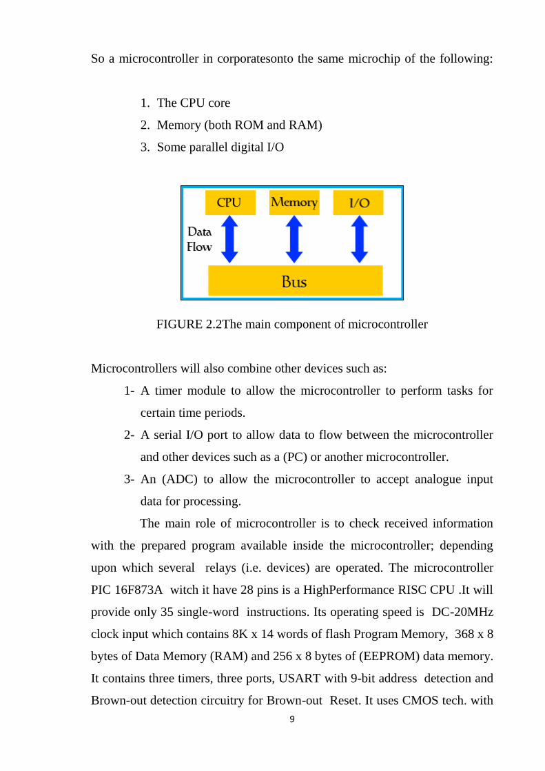
So a microcontroller in corporatesonto the same microchip of the following:
1. The CPU core
2. Memory (both ROM and RAM)
3. Some parallel digital I/O
FIGURE 2.2The main component of microcontroller
Microcontrollers will also combine other devices such as:
1- A timer module to allow the microcontroller to perform tasks for
certain time periods.
2- A serial I/O port to allow data to flow between the microcontroller
and other devices such as a (PC) or another microcontroller.
3- An (ADC) to allow the microcontroller to accept analogue input
data for processing.
The main role of microcontroller is to check received information
with the prepared program available inside the microcontroller; depending
upon which several relays (i.e. devices) are operated. The microcontroller
PIC 16F873A witch it have 28 pins is a HighPerformance RISC CPU .It will
provide only 35 single-word instructions. Its operating speed is DC-20MHz
clock input which contains 8K x 14 words of flash Program Memory, 368 x 8
bytes of Data Memory (RAM) and 256 x 8 bytes of (EEPROM) data memory.
It contains three timers, three ports, USART with 9-bit address detection and
Brown-out detection circuitry for Brown-out Reset. It uses CMOS tech. with
10
Low-power, high-speed Flash/EEPROM technology and low power
consumption.
2.5 Literature Review
The developments of a single phase inverter growth year by year as the
technologies keep changing rapidly. All electronic devices is smaller,
therefore the efficiency of power supply used in electronic devices should be
improved from time to time. Most of the researcher especially those are
experts in single phase inverter have studied and analyzed the performance of
parameter like harmonic, power losses and efficiencies of the single phase
inverter. The different switching techniques and switching elements were
used in single phase inverter also considered when inverters become the best.
Taniguchi (1988) in his thesis describe PWM technique for power
MOSFET inverter. PWM method can move unwanted frequency components
to a higher frequency region, i.e., the sidebands of a carrier frequency. Thus
the output waveform of a PWM inverter is generally improves by using a high
ratio between the carrier frequency and the output fundamental frequency.
Dimitriu (2003) in his thesis described a control with microcontroller
for PWM single phase inverter. The control principles for a PWM single
phase inverter are using the capabilities of 80C552 microcontroller. The
powerful T2 timer gives its useful feature in this application. The carrier
frequency used is 5 kHz. The result has confirmed the high quality of the
control based on microcontroller techniques.
Nicolas, B.Jun (1996).This thesis describes a sliding mode controller
for a single-phase voltage source inverter. The work is motivated by power
converter systems including two input filters with well separated corner
frequencies.
Since the inverter input current contains a low frequency component at
twice the output voltage frequency, the high frequency input filter is designed
to have low damping (no supplementary ohmic resistance).
11
The stability of the closed-loop system is ensured by the control
scheme resulting in stable large-signal behaviour while maintaining fast
dynamic response to external disturbances.
The analytical study provides general tools to design variable and
fixed-frequency control implementations. It is shown that for the voltage
source inverter, the simplest way to realise the proposed variable structure
control law consists of adding a three level disturbance signal to the switching
function. As a result, the power converter operates at constant switching
frequency in the steady-state.
The steady-state error is determined and a method is proposed to reduce
the resulting harmonic distortion of the output voltage. The static and
dynamic performances of the sliding mode controller are verified by an
experimental 5 kVA inverter
Link, U. ( 1990) This thesis describes the behavior of drives can be
improved significantly by inverters whose output provides a closed-loop
controlled AC current system of variable frequency and amplitude instead of
an open-loop controlled AC voltage. The closed-loop control detects and
compensates for the nonideal switching behavior of the power
semiconductors and for delays in the signal flow.
The author presents a description of a control system for induction
motors in inverter drives for general applications which is based on direct
closed-loop control of the inverter output currents
Zmood, D.N.( 2000). This thesis describes voltage regulation schemes
for current source inverters commonly use a simple PI stationary frame
controller but this approach is known to suffer from significant steady state
error.
In contrast, the more advanced schemes that are routinely used for
current regulation of voltage source inverters avoid these problems. This
paper presents an approach to directly utilise VSI current regulation strategies

12
to control the voltage for a CSI, without requiring significant modification or
development.
The approach uses a space vector mapping technique to convert VSI
modulation signals to CSI gate drive signals, which allows VSI closed loop
current control strategies to be directly applied to CSI voltage regulation.
Three new voltage regulation CSI controllers based on hysteresis,
synchronous frame PI and stationary frame P+resonant control principles are
presented based on this concept

13
14
CHAPTER THREE
SYSTEM DESIGN
3.1 Introduction
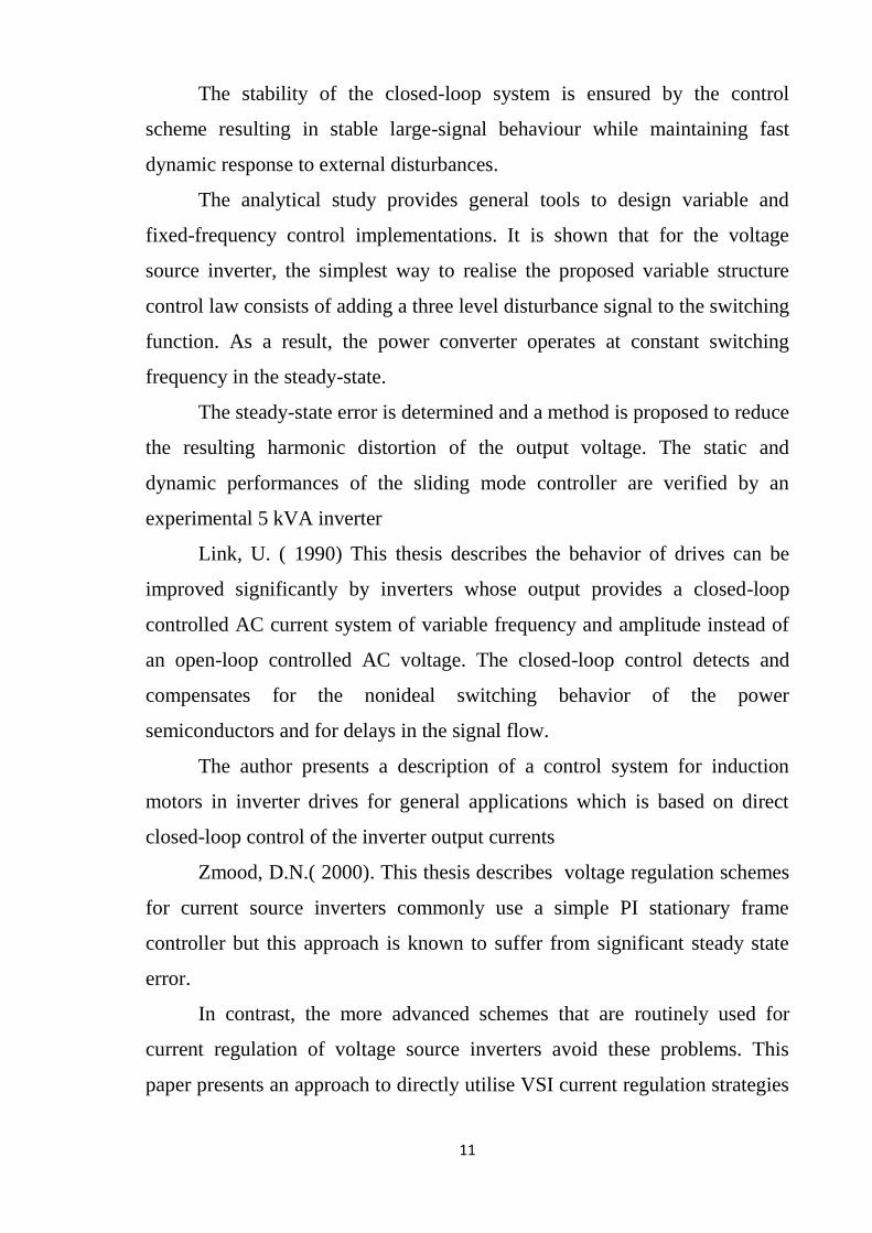
FIG 3.1 the overall block diagram of the system.
As had been seen in the above block diagram, the input of the whole
system is the buttery 12V DC .Next the fuse 2A fuse to protect the current in
case of sudden surge of high current directly come from DC supply, the next
component diode IN4001, the purpose of the diode to drive the current
voltage in one direction in case of changing the polarity the diode will plug
the current and it will be no function.
Microcontr
oller
Circuit
driver
230V
AC(fan)
TRANSFOR
MER PWM
INVERTER
12V/DC
BUTTERY
15
Following the diode is capacitor to stable the voltage. Then the voltage
regulator and the purpose of the voltage regulator is to step down the voltage
from 12V to 5 V. finally the light emitted diode LED resistance to indicate the
power supply. The PIC controller is programmed to send signal to the inverter
and get the feedback to control and stable the voltage. The micro controller is
programmed to make a control to voltage that coming from the PIC and
control the output voltage. The circuit driver start with a not gate witch
connected with PNP-NPN transistors the purpose is to switch on and off the
MOSFET.
3.2 Components:
Electronic components are the important components used to
implement the control system. This section will describe important
components used in the thesis only.
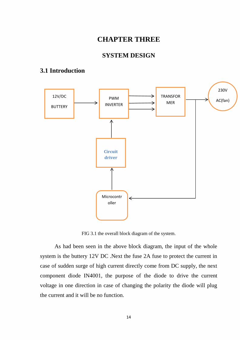
3.2.1 PIC16F873A microcontroller
FIGURE 3.2: the pins configuration of PIC 16F873A microcontroller.
Figure 3.2 shows 28 pins of 16F873A microcontroller that is used in
the thesis. This microcontroller was developed by Microchip Company. The
microcontroller has the following characteristic:
Precision internal clock oscillator
Power saving sleep mode
Has A/D converter up to 10 bit resolution
16
Need 5V DC power supply
PWM module available
This microcontroller has built.
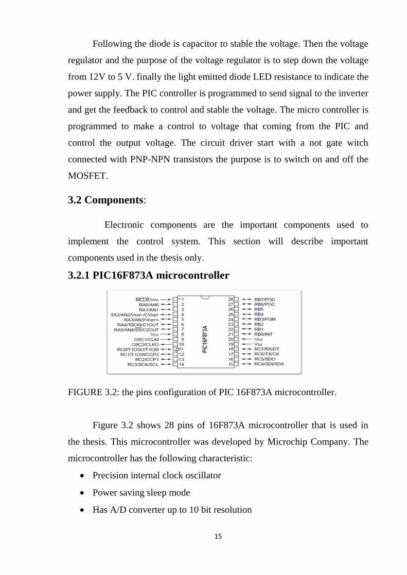
3.2.2LM7805
FIGURE 3.3 show the LM7805 voltage regulator
LM7805 voltage regulator is used to step down the DC voltage from
12 down to 5V. This voltage regulator has three terminals with the pin 1 as
shown in Figure 4.3 indicates as an input. The center pin is connected to
ground and the last pin is for output voltage. LM7805 voltage regulator is
used because of microcontroller and MAX232 IC need DC 5V. The regulator
also can operate up to 1A of current.
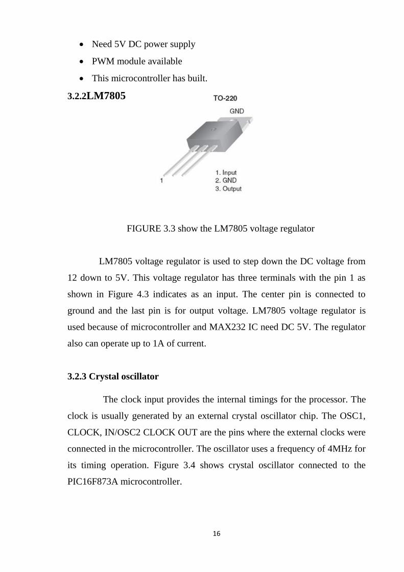
3.2.3 Crystal oscillator
The clock input provides the internal timings for the processor. The
clock is usually generated by an external crystal oscillator chip. The OSC1,
CLOCK, IN/OSC2 CLOCK OUT are the pins where the external clocks were
connected in the microcontroller. The oscillator uses a frequency of 4MHz for
its timing operation. Figure 3.4 shows crystal oscillator connected to the
PIC16F873A microcontroller.

17
FIGURE 3.4:crystal oscillator connected to the PIC16F873A microcontroller.
The period time (T) of crystal oscillator can be calculated as:
T= 1
𝑓
Where (F) is the frequency.
3.2.4 MOSFET
The full bridge inverter is most popular circuit use to convert DC to AC
spicily in high power rating. MOSFET type IRFP264 is selected as a
power switch in this thesis as shown in figure (3.). This type of MOSFET
is designed to be easily interfaced. Although the power losses in MOSFET
is low, but a heat sink is mounted on the MOSFET for heat dissipation as a
safety reason.
.
FIGURE 3.2.5 MOSFIT
P-channel of MOSFET required a complex driver circuit and the drain-
source on resistor, RDS (on) for the p-channel is higher than N-channel which

18
will lead to an increase I switching power losses which is chosen in this
thesis. Therefore n-channel MOSFET is to avoid the losses and to get the
simpler gate drive circuit.
3.2.5 Rectifier
Is an electrical device that convert alternating current AC which
periodically reverses direction current DC which flows in only one direction.
Full wave rectifiers is to converts the whole of the input waveform to one of
constant polarity at its output like the half wave circuit a full wave rectifier
circuit produces an output voltage or current which is purely DC or has some
specified DC component.Full wave rectifiers have some fundamental
advantages over the half wave rectifier counterparts. The average DC output
voltage is higher than for half wave. The output of the full wave has much
less ripple than that of the half wave producing a smoother output waveform.
3.2.6 NPN and PNP transistor
NPN and PNP two type of the bipolar transistor , NPN bipolar
transistor contains a thin p-region between two n-region .In contrast , the PNP
bipolar transistor contains a thin n-region sandwiched between two p-regions ,
The three regions and their terminal connections are called the emitter, base ,
and collector .
Figure 3.6NPN and PNP transistor
19
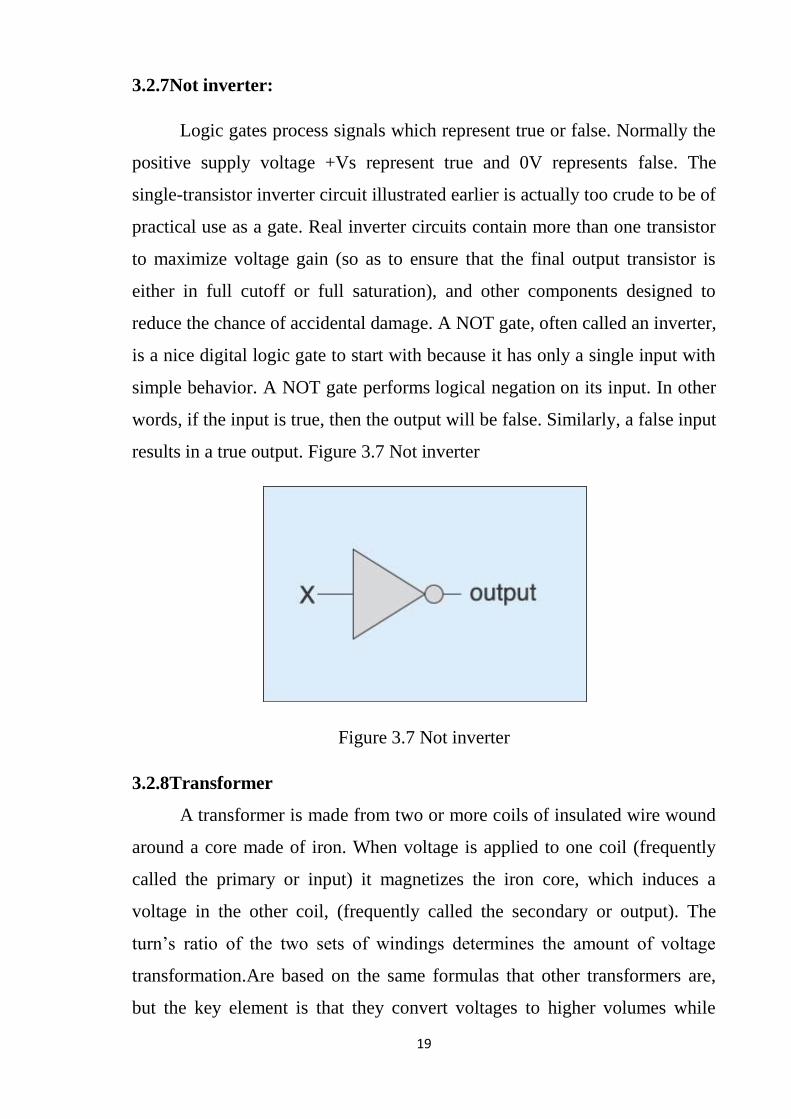
3.2.7Not inverter:
Logic gates process signals which represent true or false. Normally the
positive supply voltage +Vs represent true and 0V represents false. The
single-transistor inverter circuit illustrated earlier is actually too crude to be of
practical use as a gate. Real inverter circuits contain more than one transistor
to maximize voltage gain (so as to ensure that the final output transistor is
either in full cutoff or full saturation), and other components designed to
reduce the chance of accidental damage. A NOT gate, often called an inverter,
is a nice digital logic gate to start with because it has only a single input with
simple behavior. A NOT gate performs logical negation on its input. In other
words, if the input is true, then the output will be false. Similarly, a false input
results in a true output. Figure 3.7 Not inverter
Figure 3.7 Not inverter
3.2.8Transformer
A transformer is made from two or more coils of insulated wire wound
around a core made of iron. When voltage is applied to one coil (frequently
called the primary or input) it magnetizes the iron core, which induces a
voltage in the other coil, (frequently called the secondary or output). The
turn’s ratio of the two sets of windings determines the amount of voltage
transformation.Are based on the same formulas that other transformers are,
but the key element is that they convert voltages to higher volumes while
20
reducing amperage and effects of resistance. This makes step-up transformers
ideal in long-distance power transmission use; by stepping up voltage and
reducing amperage little energy is lost to resistance.
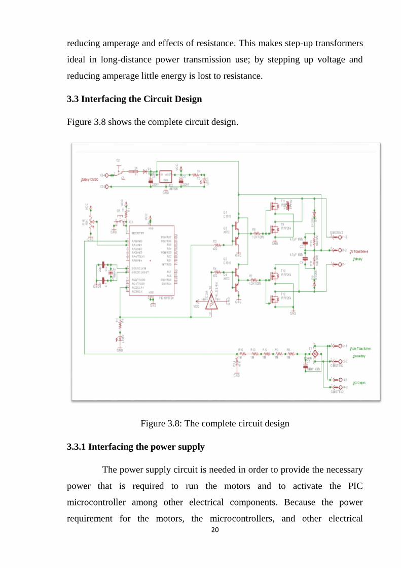
3.3 Interfacing the Circuit Design
Figure 3.8 shows the complete circuit design.
Figure 3.8: The complete circuit design
3.3.1 Interfacing the power supply
The power supply circuit is needed in order to provide the necessary
power that is required to run the motors and to activate the PIC
microcontroller among other electrical components. Because the power
requirement for the motors, the microcontrollers, and other electrical

21
components needed for this thesis is put at 5V,the supply circuit is designed
so that it does not exceed a voltage of 5V,because a voltage much higher than
5V might damage our components. The supply circuit was designed using
rectifiers, capacitors, transformer and the voltage regulator. Since the voltage
requirements of the components used for the thesis design falls under the
range of 5V,the regulator is used to step down the 5DC voltage which is the
requirement for the circuit and micro controller operation.
The above circuit shows the diagram of the supply circuit as was drawn using
the eagle software package. The component in the circuit consist of one fuse
2A, two capacitors 220 µƒ, one diode, one regular, one resistance and one led.
As shown in figure3.9. These components are connected to step down the
voltage. At the input filter is a 2A fuse to protect the current in case of sudden
surge of high current directly come from DC supply, the next component
diode IN4001, the purpose of the diode to drive the current voltage in one
direction in case of changing the polarity the diode will plug the current and it
will be no function. Following the diode is capacitor to stable the voltage.
Then the voltage regulator and the purpose of the voltage regulator is to step
down the voltage from 12V to 5 V. finally the LED resistance to indicate the
power supply is on
3.3.2 Interfacing the microcontroller and the MOSFET
Connected to the microcontroller are the input and output respectively
mostly on the left and right side of the micro controller. The crystal oscillator,
power supply all serves as the input to the PIC, while the output of the
controller is controlled by the motor as shown as figure 3.9. The PIC micro
controller I/O is 28 in number, and most of them can be used as I/O pins. The
input pins serves the purpose of connecting the power supply circuit witch I
step down the voltage from 12V/DC to 5V/DC to run the PIC the pins number
2 and 3 for controlling the frequency and voltage also pin 13 use for control
the switching on(1) and off(0) the MOSFIT.

22
The VSS/VDD pins are pins which represents the power pins. The VDD is
the positive pin while the Vssis the negative supply pin. The maximum supply
voltage that can be used for the processor is 5V while the minimum is
3.7V.Therefore based on this supply pins present in the PIC microcontroller,
it is clear that a supply is needed to be designed so as to power the
microcontroller.The purpose of using PIC is to receive and process signal
accordingly from the power supply circuit and sending it out to the motor as
output, also to feedback the output voltage to control and suitable the output
voltage.in case on this thesis we used four MOSFITS switches each of them
connected with two transistors NPN-PNP, the first two transistors was
connected directly to pin 13 and the others two connected to pin 13 through
not gate, the purpose of using not gate is to opposite the signal from 1 to 0 or
from 0 to 1.
In case when the signal that coming from the pic 13 to the transistors
that connected directly to pin 13 the signal will enter to NPN transistor then
will pass to the PNP transistor witch will be grounded, from the NPN we will
pass the signal to the MOSFIT, at the same time the not gate will receive a
signal from pin 13 and change the signal according to the first step as it
shown on the figure below. The next step the MOSFITS, the two switches
connected with two transistors (NPN, PNP) and the second two connected
with other’s two transistor witch connected with not gate to change the signal.
For example when the signal that coming from the PIC to the first two
transistors is 1 it will send the signal to MOSFITS switches then to the
transformer. The purpose of using transformer is to step up the voltage. Lastly
I Feedback the output from the transformer to the PIC pin 2 to control and
suitable the output voltage

23
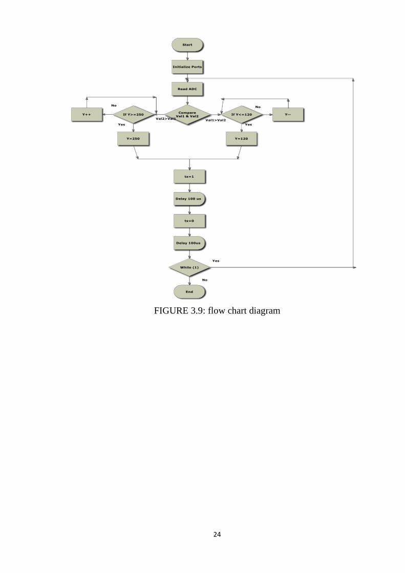
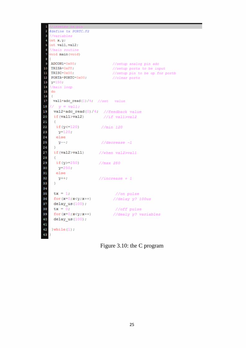
3.4 Flow Chart and the Program Function
After pressing start bottom the port will be initialize in order to make
ADC to read the values (val1 and val2) and compare it. When val1 is greater
than val2, the integer (Y) must be less or equal to 120 but incase (Y) is bigger
that 120 the integer will decrease to the point of (Y) is equal to 120 again
until satisfy this condition. On the other hand in case of val2 is bigger than
val2 the integer (Y) must be less or equal to 250 but incase (Y) is bigger that
250 the integer will decrease to the point of (Y) is equal to 250 again until
satisfy this condition.
After satisfy the condition in two cases will lead to generate the pools if
the integer is equal to one will leads to delay the (Y) that is means the pools
on and the delay will appear with 100ms and when the integer is equal to zero
will leads to delay (Y) that is mean the pools is off at delay 100ms. After all
in case the pool is on the program will return to starting point and start all
over again and incase the pool is off mode the program will end as shown in
figure 3.9 and figure 3.10,respectively.
24
FIGURE 3.9: flow chart diagram
25
Figure 3.10: the C program
26
3.5 Hardware Implementation
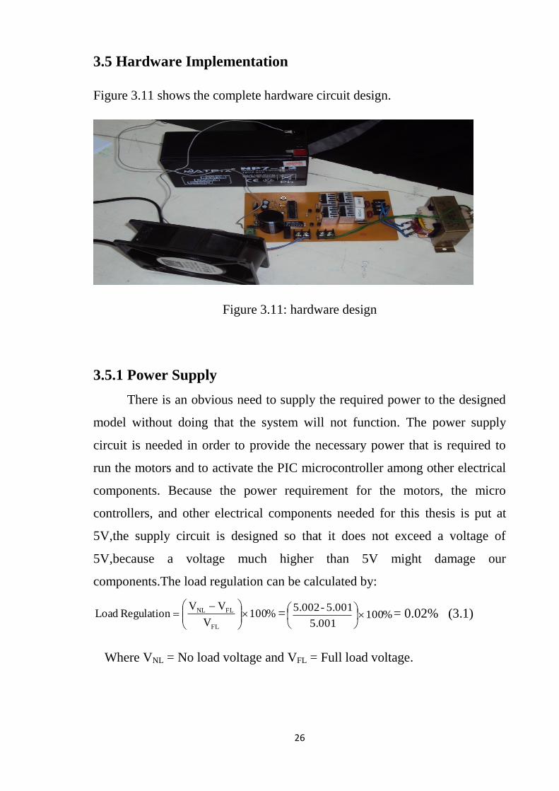
Figure 3.11 shows the complete hardware circuit design.
Figure 3.11: hardware design
3.5.1 Power Supply
There is an obvious need to supply the required power to the designed
model without doing that the system will not function. The power supply
circuit is needed in order to provide the necessary power that is required to
run the motors and to activate the PIC microcontroller among other electrical
components. Because the power requirement for the motors, the micro
controllers, and other electrical components needed for this thesis is put at
5V,the supply circuit is designed so that it does not exceed a voltage of
5V,because a voltage much higher than 5V might damage our
components.The load regulation can be calculated by:
%100V
VVRegulation Load
FL
FLNL
= %100
5.001
5.001-5.002
= 0.02% (3.1)
Where VNL = No load voltage and VFL = Full load voltage.

27
3.5.2 Controller circuit
The second test was carried out on the controller circuit, it was noticed
that the PIC 16F873A used in implementing to receive and process signal
accordingly from the power supply circuit and sending it out to the motor as
output, Also to feedback the output voltage to control and suitable the output
voltage.On this thesis used four MOSFITS switches each of them connected
with two transistors NPN-PNP, the first two transistors are connected directly
to pin 13 and the others two connected to pin 13 through NOT gate, the
purpose of using not gate is to opposite the signal from 1 to 0 or from 0 to 1.
In case when the signal that coming from the pin 13 to the transistors that
connected directly to pin 13 the signal will enter to NPN transistor then will
pass to the PNP transistor witch will be grounded, from the NPN we will pass
the signal to the MOSFIT, at the same time the NOT gate will receive a signal
from pin 13 and change the signal according to the first step also the pins
number 2 and 3 for controlling the frequency and voltage also pin 13 use for
control the switching on(1) and off(0).
3.6 Software Implementation
There are four important software’s used in the thesis.
3.6.1 MikroC Software
This is powerful software that developed by microelectronika company.
The software also has broad library functions at which programmer can
access. In general, the MikroC software allows user:
Write the C code using advanced code editor.
By using "include" function, accessing or processing of code become even
faster.
Control the execution of the program at which the "error" will be reported
when bugs are detected.

28
Samples of program also provided in the helps file.
Figure 3.12 shows C code using mikroc software.
Figure 3.12 C code using mikroc software
3.6.2 PICKit2 Software
This software is used to read and write successful HEX into PIC16F87
3A microcontroller. Before using this software, make sure the device of
programmer is connected to the computer. The programmer is shown in
Figure 3.13. Now, to burn the program inside the microcontroller, from
PICkit2 software, choose "File" "Import Hex" "Write". The command
of "Program is successfully burned" will pop out from the window.
Figure 3.13: PIC microcontroller programmer.

29
3.6.3 Protues software
This is the most useful software for checking the circuit connection and
output signal. Most of the students and electronic designers depend on this
software to check their circuit performance before actual circuit is built on
bread board and PCB. Figure 3.14 shows the complete circuit design using
protues software.
FIGURE 3.14: the complete circuit design using protues software
design
3.6.4 EAGLE PCB software
This software is used to design schematic diagram of the thesis. There
are two versions available, one is eagles PCB and the other is eagle’s
schematic diagram. Figure 3.15 and 3.16 shows the window of PCB eagles
and its schematic window, respectively.

30
Figure 3.15: Eagle’s PCB window
Figure 3.16: Eagles schematic window.
The eagles PCB software is used to design the PCB layout based on the
schematic diagram. Both of these software, eagles PCB and schematic do
have function to simulate. Therefore, user cannot check his/her design
schematic diagram output signal. Figure 3.17shows the PCB layout of over
current protection.

31
Figure 3.17shows the PCB layout of over current protection.
The following procedures shown how to the PCB is made:
1. Print out the PCB layout using laser printer and transparency.
2. Using ironing method to transfer the image of print out onto PCB board.
3. Use iron(III) chloride to do the wet chemical etching.
4. Use alcohol solution to clean the PCB.
5. Use driller to drill the holes on the PCB.
6. Assembly the components and solder it.
7. Trim the components legs.

32

33
CHAPTER FOUR
RESULT AND DISCUSSION
4.1 Introduction
In this chapter, result are presented to evaluate the performance of the
proposed system.
4.2 AC Voltage Output Sinusoidal Wave
In order to verify the validity of the proposed system, several practical testes
are carried out.
4.2.1 Scenario one
The output voltage = 128.2 AC/V
R = 1.6 KΩ
Output or load current = 0.075 1
Output or load current = 0.078 2
Calculated output = 0.08
Figure 4.1 shows the output AC voltage reading under case one
Figure 4.1: the output ac voltage reading under case one
34
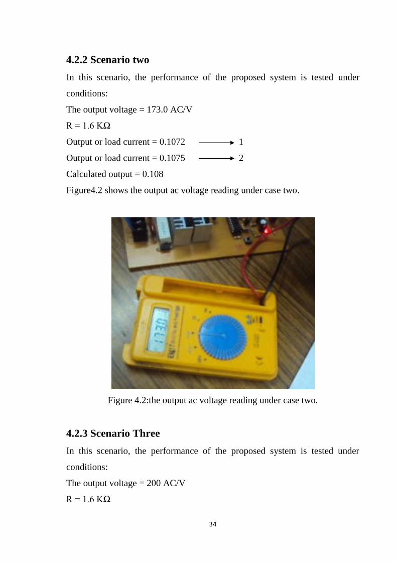
4.2.2 Scenario two
In this scenario, the performance of the proposed system is tested under
conditions:
The output voltage = 173.0 AC/V
R = 1.6 KΩ
Output or load current = 0.1072 1
Output or load current = 0.1075 2
Calculated output = 0.108
Figure4.2 shows the output ac voltage reading under case two.
Figure 4.2:the output ac voltage reading under case two.
4.2.3 Scenario Three
In this scenario, the performance of the proposed system is tested under
conditions:
The output voltage = 200 AC/V
R = 1.6 KΩ
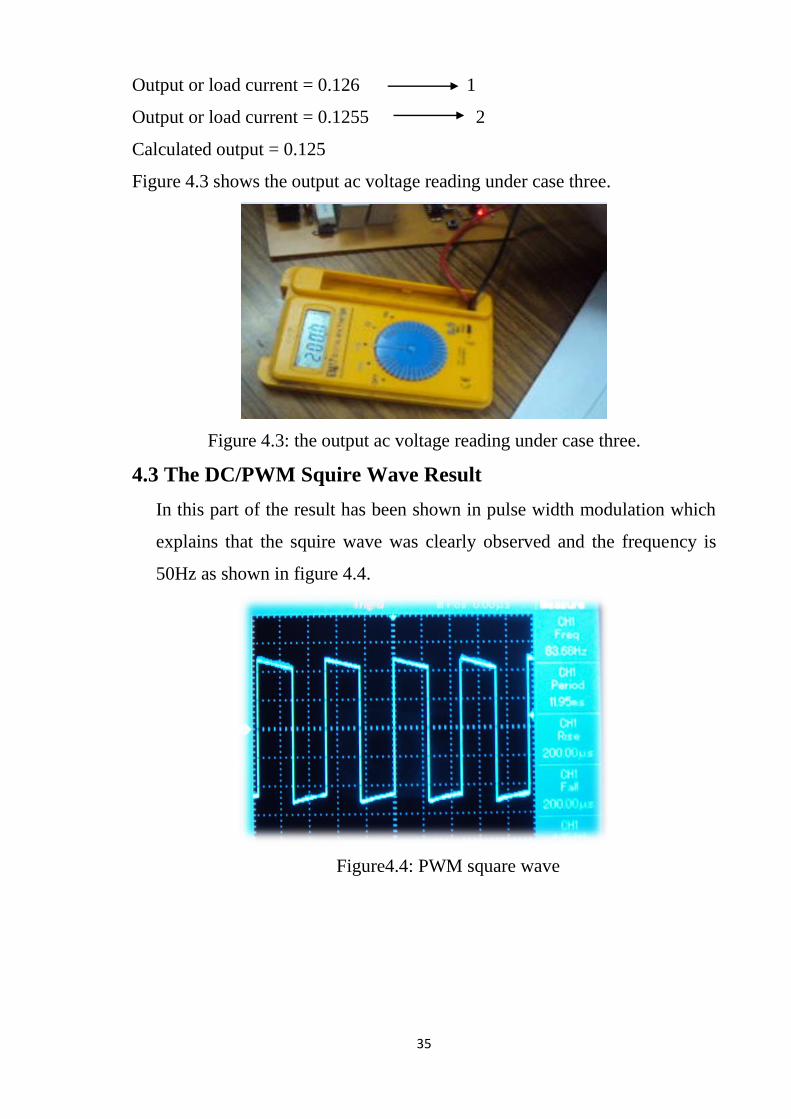
35
Output or load current = 0.126 1
Output or load current = 0.1255 2
Calculated output = 0.125
Figure 4.3 shows the output ac voltage reading under case three.
Figure 4.3: the output ac voltage reading under case three.
4.3 The DC/PWM Squire Wave Result
In this part of the result has been shown in pulse width modulation which
explains that the squire wave was clearly observed and the frequency is
50Hz as shown in figure 4.4.
Figure4.4: PWM square wave

36

37
CHAPTER FIVE
CONCLUSION AND RECOMMENDATION
5.1 Conclusion:
The major aim of thesis was to develop a single-phase inverter using PIC
16F873A. The thesis was successfully implemented and designed the single
phase inverter with PIC controller build the circuit hardware by using
MOSFETs P Chanel type IRFP264. The design of driver circuit has illustrated
to switch the MOSFET. However the Feedback output voltage from the
transformer to the micro which already controlled and suitably for the output
voltage. In conclusion based on the finding from this thesis, all the designed
single phase inverter has their respective function, in situation where better to
convert from 12v DC to AC 120 at minimum and 200 maximum which
controls the full bridge switch by generating the pulse with the PIC controller
and step up the voltage by using transformer.
5.2 Recommendation:
The results of this thesis open some interesting and challenging
problems of great importance. In what follows, some of the possible future
works are listed:
A. Deep understanding of the importance of voltage source inverter as
well as future design tools would make it quite simple to convert the
DC to AC and using one pin from the microcontroller to run the
MOSFETs.
B. Make this particular pin by adding not inverter and PNP, NPN
transistors to change the pulse from one to zero or the opposite in order
to switch the MOSFETs on or off.

38
REFERENCES
[1] Budak, A. passive and Active Analysis and Synthesis. Houghton Mifflin,
Boston, MA, 2013.
[2] Cho,D., Kato, Y. and Spilman, D.Sliding Mode and Classical Controllers
in
Magnetic Levitation Systems. IEEE Control Systems, February 2003, pp. 42 -
48.
[3] D' Azzo, J.J, and Houpis, C.H. Feedback Control System Analysis and
Synthesis, 2ed. McGraw-Hill, New York, 2010.
[4] Dorf, R.C. Modern Control Systems, 5th ed. Addison-Wesley, Reading,
MA, 2015.
[5] Hostetter, G.H., Design of Feedback Control Systems, 2ed. Saunders
College Publishing, New York, 2015.
[6] Aggarwal, J.K. "Introduction of DC motor," Special Issue, IEEE Trans.
DC Motor Control, vol. PAMI-2, no.6, pp. 493 - 588, 1980.
[7] Agin,G.J. "DC motor working principle," Memo AIM-173, Motor Control
[8]V.Birunda Mary, Dr.I.William Christopher, switch single phase
inverter,1st international conference on power engineering, computing and
control, PECCON-2017 published by Elsevier Ltd.
[9]BILAL,Single phase voltage source inverter simulation, Published 2017