Embed Size (px)
Citation preview
D.D.D.D. K.K.K.K. TiwariTiwariTiwariTiwari et alet alet alet al. Nano Studies, 201. Nano Studies, 201. Nano Studies, 201. Nano Studies, 2013333, , , , 8888, , , , 53535353----62626262....
53535353
NANOCRYSTALLINE NICKEL COBALT FERRITE (NANOCRYSTALLINE NICKEL COBALT FERRITE (NANOCRYSTALLINE NICKEL COBALT FERRITE (NANOCRYSTALLINE NICKEL COBALT FERRITE (NiNiNiNi1/21/21/21/2CoCoCoCo1/21/21/21/2FeFeFeFe2222OOOO4444) FOR) FOR) FOR) FOR
ELECTROMAGNETICELECTROMAGNETICELECTROMAGNETICELECTROMAGNETIC INTERFERENCE (EMI) SHIELDING APPLICATIONSINTERFERENCE (EMI) SHIELDING APPLICATIONSINTERFERENCE (EMI) SHIELDING APPLICATIONSINTERFERENCE (EMI) SHIELDING APPLICATIONS
D.D.D.D. K.K.K.K. TiwariTiwariTiwariTiwari 1111, , , , A.A.A.A. K.K.K.K. ThakurThakurThakurThakur 2222,,,, S.S.S.S. E.E.E.E. BorjasBorjasBorjasBorjas––––GarcíaGarcíaGarcíaGarcía 1111,,,, L.L.L.L. M.M.M.M. VillaseñorVillaseñorVillaseñorVillaseñor CendejasCendejasCendejasCendejas 1111, N., N., N., N. DasguptaDasguptaDasguptaDasgupta––––SchubertSchubertSchubertSchubert 1111
1 Universidad Michoacana de San Nicolás de Hidalgo
Morelia, México [email protected]
2 Indian Institute of Technology Kharagpur Kharagpur, India
Accepted September 19, 2013Accepted September 19, 2013Accepted September 19, 2013Accepted September 19, 2013
1. Introduction1. Introduction1. Introduction1. Introduction
The role of electromagnetic field is predominantly very much crucial to determine the content and quality of data transfer at very high frequency ranges. The number of electromagnetic signals has increased with the advancement of technology and its ever growing use in telecommunication, biomedical and other electronic systems causes a serious issue due to electromagnetic interference (EMI). EMI is high frequency signal, disturbs the function of a circuit, cable or other electronic component originated from other equipment or from the self-affected components [1, 2]. The EMI caused by these signals necessitate protective materials to avoid diminished product performance or product failure. EMI is coupled between circuits or equipment having some mutual impedance through which one circuit can affects the other circuit [3]. The mutual impedance can be conductive, capacitive, inductive, or combination of these. When electromagnetic energy affects any equipment adversely by causing it to have an emergent response then this electromagnetic energy is called EMI and the affected equipment is said to be susceptible to EMI. EMI may leave a source or enter susceptible equipment by conduction, coupling, or radiation. Interference occurs between one part of the equipment to another or through power supply to nearby circuits [3]. EMI is conducted via signal lines, antenna leads, power cables, and even ground connections, between EMI sources and EMI-susceptible equipment.
EMI shielding makes plastic enclosures to protect equipment with EMI; also, increases emphasis on სtorage, protection and safe transmission of data, such as, cyber security, crime prevention [1, 2]. EMI shielding reflects, absorbs or transmits the electromagnetic waves to prevent interference from a particular device or zone via an effective placement of shielding materials to reduce the level of electromagnetic energy radiated by the equipment. There are many kind of materials are used for removal or minimization of EMI shielding e.g. sheet metal, conductive paints, electroless plating, ferrites, polymers, composites, etc.
The materials used for EMI shielding are; sheet metal, conductive paint, electroless plating, conductive plastics and ferrites. Depending on the materials property there are certain limitations regarding their design versatility and environmental reliability. Ferrite designs are
Nanocrystalline nickel cobalt ferrite (Nanocrystalline nickel cobalt ferrite (Nanocrystalline nickel cobalt ferrite (Nanocrystalline nickel cobalt ferrite (NNNNiiii1/21/21/21/2CCCCoooo1/21/21/21/2FFFFeeee2222OOOO4444) for ) for ) for ) for ............ ((((EMIEMIEMIEMI) shielding applications) shielding applications) shielding applications) shielding applications....
54545454
made with solid and split beads arranged in versatile geometries and with many types of material compounds, and they offer many installation alternatives. The shielding property of ferrites is strongly influenced by the chemical composition, crystalline structure, grain size, nature of porosity, secondary phase thickness of the grain boundary, magneto crystalline anisotropy and magnetostriction. Electrical characteristics of these components depend on the geometry of conductive material and permeability of the core material.
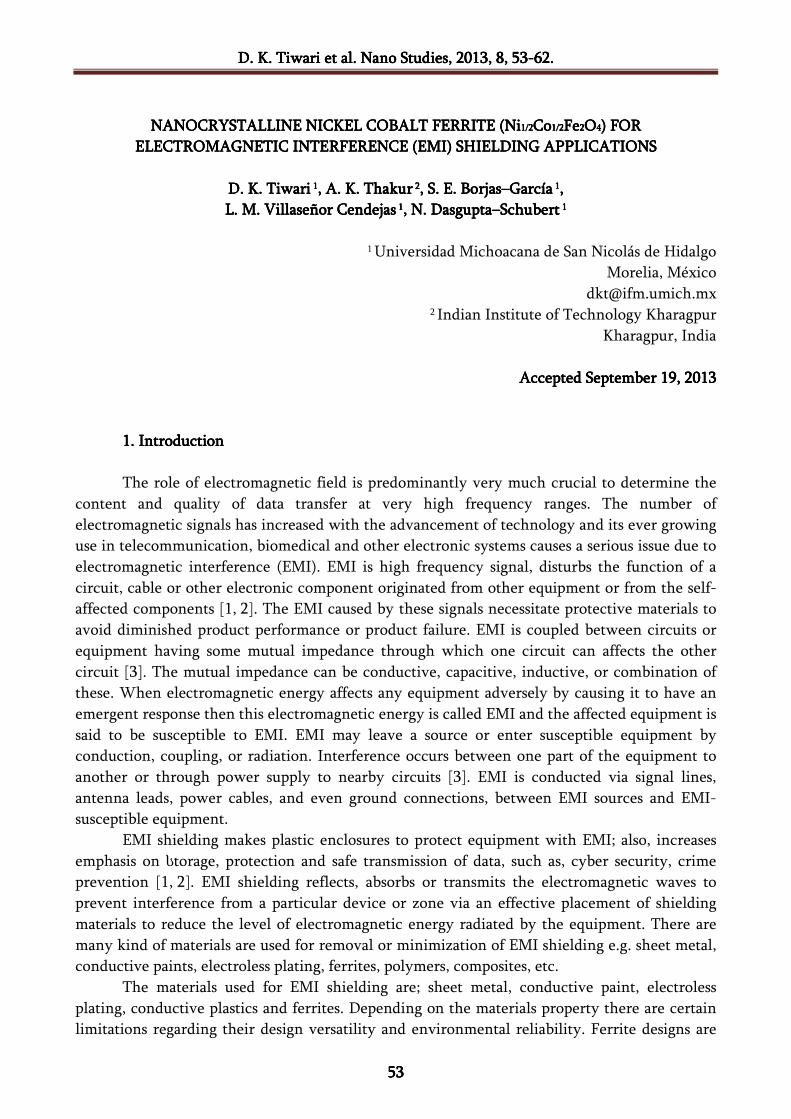
EMI shielding measures in term of shielding effectiveness (SE) which is defined in decibel (dB), as the ratio of the electric / magnetic field that is incident on the barrier to the magnitude of electric / magnetic field that is transmitted through the barrier (FigureFigureFigureFigure 1111) [4, 5]:
SE00
log20log10E
E
P
P ii == , (1)
where iE and 0E are incident and transmitted electric fields respectively.
SE as given by the above equation can also be divided into three terms of reflection loss, absorption loss and multiple reflections, i.e.
SE BAR ++= , (2) where R = reflection loss caused by reflection at the left and right interfaces; A = absorption loss of the wave as it proceeds through the barrier; B = multiple reflections and transmissions.
FigureFigureFigureFigure 1111.... EMI shielding pattern.
The multiple reflections and transmissions can be neglected because of the shield thicknesses that are much greater than skin depth, so that the effective parameter which will affect the SE only initial reflection and transmission at the left and right interfaces [5, 6], i.e.
SE RA += . (3)
Absorption lossAbsorption lossAbsorption lossAbsorption loss Absorption loss of a sample can be defined as
δ
tA explog20= , (4)
where, t is thickness of the sample and δ is the skin depth, which can be defined as
µσπµωσ
δf
12== (5)
D.D.D.D. K.K.K.K. TiwariTiwariTiwariTiwari et alet alet alet al. Nano Studies, 201. Nano Studies, 201. Nano Studies, 201. Nano Studies, 2013333, , , , 8888, , , , 53535353----62626262....
55555555
when σ ωε>> , and
2 εδ
σ µ= (6)
when σ ωε<< , so that
δδ
tx
tA 7.8explog20 == , ((((7)
27.8
µσωtA = (8)
or
rrftftA σµµσπ 1317.8 == . (9)
Reflection lossReflection lossReflection lossReflection loss The reflection loss depends on the mismatch between the incident wave impedance and
the impedance of the shield. Ignoring the multiple reflections, the reflection loss for a plane wave of frequency f can be defined as
r
r f
fR
σ
µ
µ
σlog10168log105.31 −=+= . (10)
From equation (3), (9) and (10), SE can be calculated with the formula:
SEr
rrr
fft
σ
µσµ log10168131 −+= , (11)
where, rσ is the conductivity of the material relative to copper, f is the frequency in Hz and
rµ is the relative permeability.
SE can also be defined for the composite materials using Simon formula:
SE σσ
ftf
7.1log1050 ++= , (12)
where σ is the conductivity of the material (S / cm), t is the thickness of the sample in cm, and f is the frequency (MHz) of the electromagnetic radiation. The first two terms of equation
(12 ) represent the reflection loss and the third term is the absorption loss.
2. 2. 2. 2. ExperimentalExperimentalExperimentalExperimental
2.1. 2.1. 2.1. 2.1. Material Material Material Material ppppreparationreparationreparationreparation
Nanocrystalline Ni1/2Co1/2Fe2O4 powers were prepared using citrate route method [7]. The chemical reaction of the material preparation has been noted in equation (13):
½ Ni(NO3)2 · 6 H2O + ½ Co(NO3)2 · 6 H2O + 2 Fe(NO3)2 · 9 H2O +C6H8O7 · H2O → → Ni1/2Co1/2Fe2O4 + 6 CO2 + 8 NH4OH + 16 O2 + 9 H2. (13)
The precursors citric acid, nickel, cobalt and iron nitrates were dissolved in distilled water to prepare the Ni – Co ferrite. The resulting solution was heated mechanically on magnetic stirrer at 50 °C for 1 h and final suspension was filtered adding NH4OH after fixing pH at 10. The precipitate was washed, dried and calcined for 3 h at 300 °C. Homogeneous powders were obtained after milling in mortar about 15 – 20 min.
Nanocrystalline nickel cobalt ferrite (Nanocrystalline nickel cobalt ferrite (Nanocrystalline nickel cobalt ferrite (Nanocrystalline nickel cobalt ferrite (NNNNiiii1/21/21/21/2CCCCoooo1/21/21/21/2FFFFeeee2222OOOO4444) for ) for ) for ) for ............ ((((EMIEMIEMIEMI) shielding applications) shielding applications) shielding applications) shielding applications....
56565656
2.2. 2.2. 2.2. 2.2. Pellet Pellet Pellet Pellet ppppreparationreparationreparationreparation
The pellets were prepared using 1 % wax as a binding agent at 6 ton / cm2 pressures. The
selected die-punch has area 133 mm2. The pellets have diameter 13.06 mm and thickness 2.13 mm.
2.3. 2.3. 2.3. 2.3. CCCCharacterizationharacterizationharacterizationharacterization
The crystal structure and particle size of prepared sample is characterized by X-ray diffraction (XRD) pattern by using X-ray diffractometer Rigakuminiflex (Japan) and the particle size were calculated using Scherer’s formula:
0.9
cos B
Dλ
β θ= , (14)
where D = particle size; λ = X-ray wavelength; β = full width at half max (FWHM) and Βθ =
Bragg angle. The structural and morphological property of the prepared material is analysed using
transmission electron microscope (TEM) Philips CM 12 at 25 and 50 kV. TEM had been carried out by ultrasonic dispersion of powder samples in acetone and placing a small drop on thin carbon film supported on the copper grid until it dry.
Electrical property of the material is characterized using impedance analyser (Hioki 3522–50 LCRHiTESTER, Hioki 9700–10 Head Amp Unit). The sample is sandwiched between two electrodes, which measure the impedance as a function of frequency of the applied signal. The apparatus evaluate and separates contribution to the overall electrical properties in the frequency domain due to electrode reaction at the electrode interface and the migration of ions through the bulk and across the grain boundaries of materials. Variation of relative permeability component with respect to frequency was calculated using Agilent 4294 A precision impedance analyser at current 10 mA. The pellet sample was placed as a coil and an electric current 10mA were applied in transverse direction of the placed sample. The flowing current produces a magnetic field, hence a magnetic flux generated through the circuit and the ratio of the magnetic flux to the current will give the inductance ( L ) of the circuit. The real and imaginary parts of the permeability components can be calculated using
0L
Ls=′µ (15)
and
0
0
2 Lf
RRs
πµ
−=′′ , (16)
where, sL is the inductance of the coil in presence of pellet sample, 0L inductance of the empty
coil (without sample), sR is the coil resistance in presence of sample, 0R is resistance of coil
without sample and f is the frequency.
Magnetic loss tangent can be calculated using formula:
µ
µδ
′
′′=tan . (17)
D.D.D.D. K.K.K.K. TiwariTiwariTiwariTiwari et alet alet alet al. Nano Studies, 201. Nano Studies, 201. Nano Studies, 201. Nano Studies, 2013333, , , , 8888, , , , 53535353----62626262....
57575757
3. Results and discussion3. Results and discussion3. Results and discussion3. Results and discussion
3.1. 3.1. 3.1. 3.1. Crystal Crystal Crystal Crystal sssstructure and tructure and tructure and tructure and ppppowder owder owder owder ssssize of ize of ize of ize of pppprepared Nirepared Nirepared Nirepared Ni –––– Co Co Co Co fffferriteerriteerriteerrite
The material preparation and single-phase formation of Ni – Co ferrite (Ni½Co½Fe2O4)
samples were confirmed by XRD pattern and POWD technique was used to analyse the lattice parameter ( a ). TableTableTableTable 1111 shows the Miller indices values of the obtained peaks with respective angle ( θ2 ) and the material shows cubic structure [8] with lattice parameter value 8.3584 Å. The formation of the material is confirmed by JCPDS no. 742081 [7]. Powder of the prepared nickel–cobalt ferrite (Ni1/2Co1/2Fe2O4) is calculated by Scherer’s formula, obtained 27.7 nm, which confirms the prepared material is nanocrystalline.
TableTableTableTable 1111.... XRD Pattern of prepared samples using POWD analytical technique.
Angle θ2 , °
Miller indices ),,( lkh
Lattice parameter a , Å
30.26
(2, 2, 0)
8.3584
35.62
(3, 1, 1)
43.26
(4, 0, 0)
53.64
(4, 2, 2)
cubic structure
57.25
(5, 1, 1)
62.86
(4, 4, 0)
74.31
(5, 3, 3)
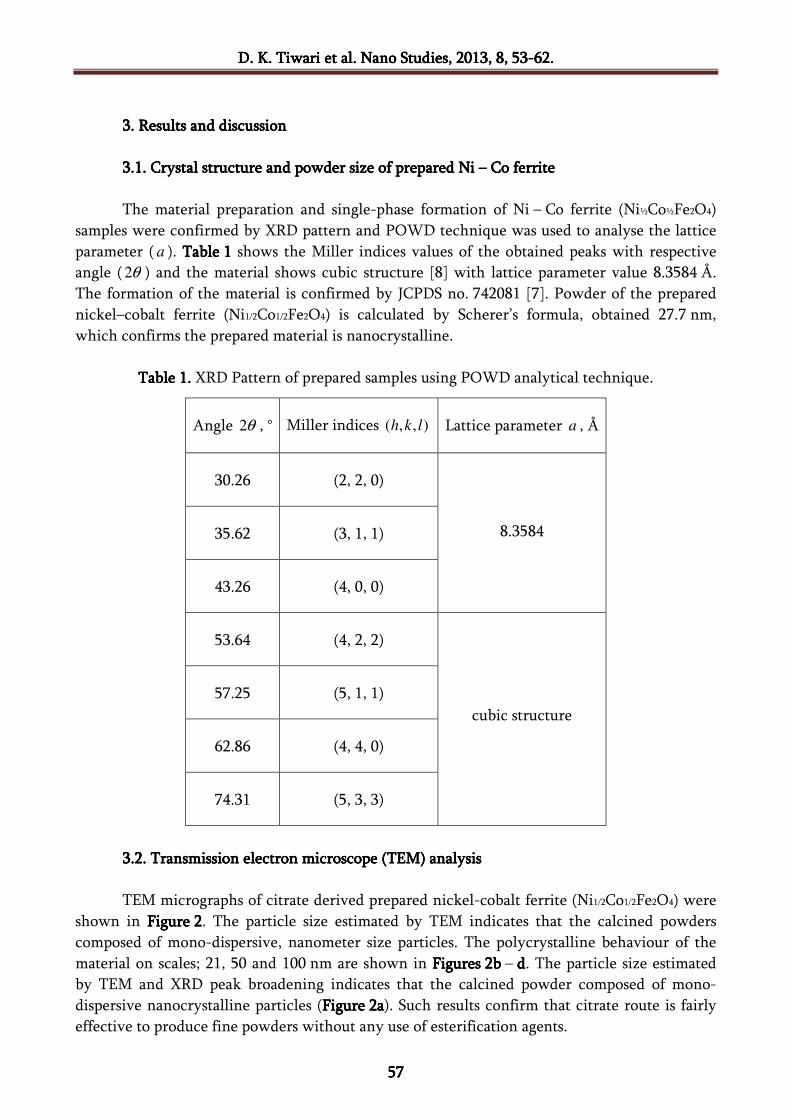
3.2. 3.2. 3.2. 3.2. Transmission Transmission Transmission Transmission eeeelectron lectron lectron lectron mmmmicroscope (TEM) icroscope (TEM) icroscope (TEM) icroscope (TEM) aaaanalysisnalysisnalysisnalysis
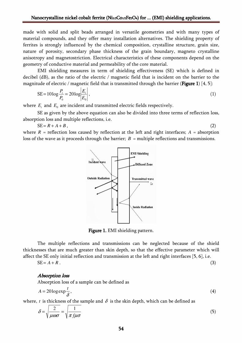
TEM micrographs of citrate derived prepared nickel-cobalt ferrite (Ni1/2Co1/2Fe2O4) were
shown in FigureFigureFigureFigure 2222. The particle size estimated by TEM indicates that the calcined powders composed of mono-dispersive, nanometer size particles. The polycrystalline behaviour of the material on scales; 21, 50 and 100 nm are shown in FigureFigureFigureFiguressss 2b2b2b2b – dddd. The particle size estimated by TEM and XRD peak broadening indicates that the calcined powder composed of mono-dispersive nanocrystalline particles (FigureFigureFigureFigure 2a2a2a2a). Such results confirm that citrate route is fairly effective to produce fine powders without any use of esterification agents.
Nanocrystalline nickel cobalt ferrite (Nanocrystalline nickel cobalt ferrite (Nanocrystalline nickel cobalt ferrite (Nanocrystalline nickel cobalt ferrite (NNNNiiii1/21/21/21/2CCCCoooo1/21/21/21/2FFFFeeee2222OOOO4444) for ) for ) for ) for ............ ((((EMIEMIEMIEMI) shielding applications) shielding applications) shielding applications) shielding applications....
58585858
FigureFigureFigureFigure 2222.... TEM of Ni1/2Co1/2Fe2O4.
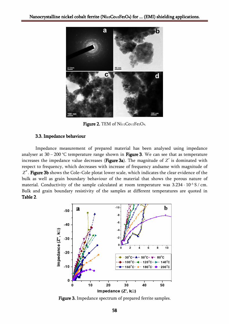
3.3. 3.3. 3.3. 3.3. Impedance Impedance Impedance Impedance bbbbehaviourehaviourehaviourehaviour
Impedance measurement of prepared material has been analysed using impedance analyser at 30 – 200 °C temperature range shown in FigureFigureFigureFigure 3333. We can see that as temperature increases the impedance value decreases (FigureFigureFigureFigure 3a3a3a3a). The magnitude of Z ′ is dominated with respect to frequency, which decreases with increase of frequency andsame with magnitude of Z ′′ . FigureFigureFigureFigure 3b3b3b3b shows the Cole–Cole plotat lower scale, which indicates the clear evidence of the bulk as well as grain boundary behaviour of the material that shows the porous nature of material. Conductivity of the sample calculated at room temperature was 3.234 · 10–5 S / cm. Bulk and grain boundary resistivity of the samples at different temperatures are quoted in TableTableTableTable 2222.
FigureFigureFigureFigure 3333.... Impedance spectrum of prepared ferrite samples.
D.D.D.D. K.K.K.K. TiwariTiwariTiwariTiwari et alet alet alet al. Nano Studies, 201. Nano Studies, 201. Nano Studies, 201. Nano Studies, 2013333, , , , 8888, , , , 53535353----62626262....
59595959
TableTableTableTable 2.2.2.2. Resistivity of material with temperature.
Temperature, °C Bulk resistivity, Ohm · cm GB resistivity, Ohm · cm 30 3.09 · 104 8.93 · 105 50 2.52 · 104 6.97 · 105 80 1.67 · 104 6.00 · 105
100 1.49 · 104 5.89 · 105 120 1.30 · 104 5.10 · 105 140 1.20 · 104 4.28 · 105 160 1.15 · 104 2.90 · 105 180 1.03 · 104 1.25 · 105 200 9.83 · 103 8.24 · 104
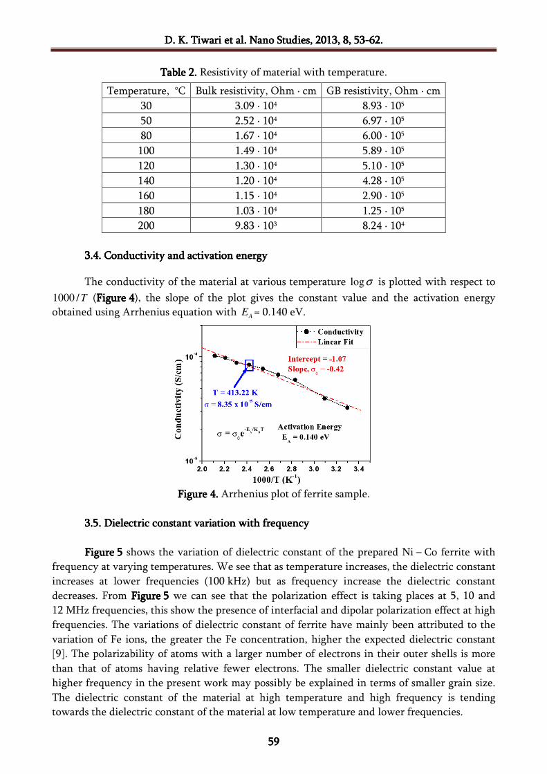
3.4. 3.4. 3.4. 3.4. Conductivity and Conductivity and Conductivity and Conductivity and aaaactivation ctivation ctivation ctivation eeeenergynergynergynergy
The conductivity of the material at various temperature σlog is plotted with respect to
T/1000 (FigureFigureFigureFigure 4444), the slope of the plot gives the constant value and the activation energy obtained using Arrhenius equation with AE = 0.140 eV.
FigureFigureFigureFigure 4444.... Arrhenius plot of ferrite sample.
3.5. 3.5. 3.5. 3.5. Dielectric Dielectric Dielectric Dielectric cccconstantonstantonstantonstant vvvvariation with ariation with ariation with ariation with ffffrequencyrequencyrequencyrequency
FigureFigureFigureFigure 5555 shows the variation of dielectric constant of the prepared Ni – Co ferrite with
frequency at varying temperatures. We see that as temperature increases, the dielectric constant increases at lower frequencies (100 kHz) but as frequency increase the dielectric constant decreases. From FigureFigureFigureFigure 5555 we can see that the polarization effect is taking places at 5, 10 and 12 MHz frequencies, this show the presence of interfacial and dipolar polarization effect at high frequencies. The variations of dielectric constant of ferrite have mainly been attributed to the variation of Fe ions, the greater the Fe concentration, higher the expected dielectric constant [9]. The polarizability of atoms with a larger number of electrons in their outer shells is more than that of atoms having relative fewer electrons. The smaller dielectric constant value at higher frequency in the present work may possibly be explained in terms of smaller grain size. The dielectric constant of the material at high temperature and high frequency is tending towards the dielectric constant of the material at low temperature and lower frequencies.
Nanocrystalline nickel cobalt ferrite (Nanocrystalline nickel cobalt ferrite (Nanocrystalline nickel cobalt ferrite (Nanocrystalline nickel cobalt ferrite (NNNNiiii1/21/21/21/2CCCCoooo1/21/21/21/2FFFFeeee2222OOOO4444) for ) for ) for ) for ............ ((((EMIEMIEMIEMI) shielding applications) shielding applications) shielding applications) shielding applications....
60606060
FigureFigureFigureFigure 5555.... Dielectric constant variation
with frequency at different temperatures.
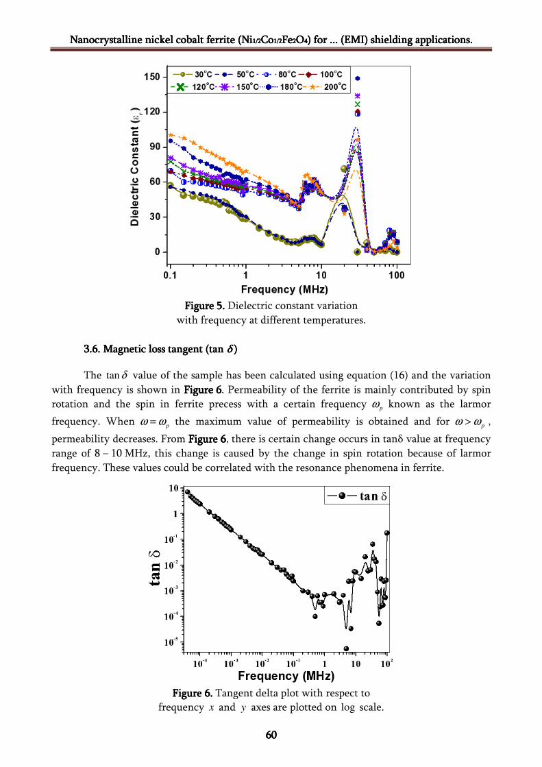
3.6. 3.6. 3.6. 3.6. Magnetic Magnetic Magnetic Magnetic lllloss oss oss oss ttttangent (angent (angent (angent (tantantantan δδδδ ))))
The δtan value of the sample has been calculated using equation (16) and the variation with frequency is shown in FigureFigureFigureFigure 6666. Permeability of the ferrite is mainly contributed by spin rotation and the spin in ferrite precess with a certain frequency pω known as the larmor
frequency. When pωω = the maximum value of permeability is obtained and for pωω > ,
permeability decreases. From FigureFigureFigureFigure 6666, there is certain change occurs in tanδ value at frequency range of 8 – 10 MHz, this change is caused by the change in spin rotation because of larmor frequency. These values could be correlated with the resonance phenomena in ferrite.
FigureFigureFigureFigure 6666.... Tangent delta plot with respect to
frequency x and y axes are plotted on log scale.
D.D.D.D. K.K.K.K. TiwariTiwariTiwariTiwari et alet alet alet al. Nano Studies, 201. Nano Studies, 201. Nano Studies, 201. Nano Studies, 2013333, , , , 8888, , , , 53535353----62626262....
61616161
3.7. 3.7. 3.7. 3.7. Shielding Shielding Shielding Shielding eeeeffectiveness ffectiveness ffectiveness ffectiveness
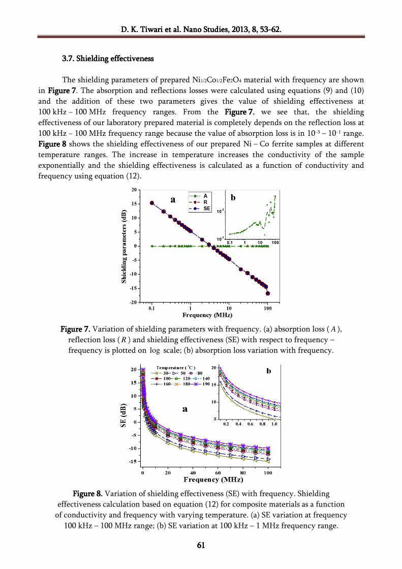
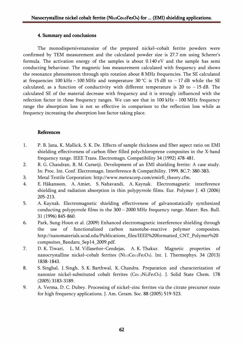
The shielding parameters of prepared Ni1/2Co1/2Fe2O4 material with frequency are shown in FigureFigureFigureFigure 7777. The absorption and reflections losses were calculated using equations (9) and (10) and the addition of these two parameters gives the value of shielding effectiveness at 100 kHz − 100 MHz frequency ranges. From the FigureFigureFigureFigure 7777, we see that, the shielding effectiveness of our laboratory prepared material is completely depends on the reflection loss at 100 kHz − 100 MHz frequency range because the value of absorption loss is in 10–3 – 10–1 range. FigureFigureFigureFigure 8888 shows the shielding effectiveness of our prepared Ni – Co ferrite samples at different temperature ranges. The increase in temperature increases the conductivity of the sample exponentially and the shielding effectiveness is calculated as a function of conductivity and frequency using equation (12).
FigureFigureFigureFigure 7777.... Variation of shielding parameters with frequency. (a) absorption loss ( A ), reflection loss ( R ) and shielding effectiveness (SE) with respect to frequency – frequency is plotted on log scale; (b) absorption loss variation with frequency.
FigureFigureFigureFigure 8888.... Variation of shielding effectiveness (SE) with frequency. Shielding effectiveness calculation based on equation (12) for composite materials as a function
of conductivity and frequency with varying temperature. (a) SE variation at frequency 100 kHz – 100 MHz range; (b) SE variation at 100 kHz – 1 MHz frequency range.
Nanocrystalline nickel cobalt ferrite (Nanocrystalline nickel cobalt ferrite (Nanocrystalline nickel cobalt ferrite (Nanocrystalline nickel cobalt ferrite (NNNNiiii1/21/21/21/2CCCCoooo1/21/21/21/2FFFFeeee2222OOOO4444) for ) for ) for ) for ............ ((((EMIEMIEMIEMI) shielding applications) shielding applications) shielding applications) shielding applications....
62626262
4. 4. 4. 4. Summary Summary Summary Summary and cand cand cand conclusionsonclusionsonclusionsonclusions
The monodispersivenanosize of the prepared nickel–cobalt ferrite powders were confirmed by TEM measurement and the calculated powder size is 27.7 nm using Scherer’s formula. The activation energy of the samples is about 0.140 eV and the sample has semi conducting behaviour. The magnetic loss measurement calculated with frequency and shows the resonance phenomenon through spin rotation about 8 MHz frequencies. The SE calculated at frequencies 100 kHz – 100 MHz and temperature 30 °C is 15 dB to – 17 dB while the SE calculated, as a function of conductivity with different temperature is 20 to – 15 dB. The calculated SE of the material decrease with frequency and it is strongly influenced with the refection factor in these frequency ranges. We can see that in 100 kHz – 100 MHz frequency range the absorption loss is not so effective in comparison to the reflection loss while as frequency increasing the absorption loss factor taking place.
ReferencesReferencesReferencesReferences 1. P. B. Jana, K. Mallick, S. K. De. Effects of sample thickness and fiber aspect ratio on EMI
shielding effectiveness of carbon fiber filled polychloroprene composites in the X-band frequency range. IEEE Trans. Electromagn. Compatibility 34 (1992) 478-481.
2. R. G. Chandran, R. M. Cursetji. Development of an EMI shielding ferrite: A case study. In: Proc. Int. Conf. Electromagn. Interference & Compatibility. 1999, 8C.7: 380-383.
3. Metal Textile Corporation: http://www.metexcorp.com/emirfi_theory.cfm. 4. E. Håkansson, A. Amiet, S. Nahavandi, A. Kaynak. Electromagnetic interference
shielding and radiation absorption in thin polypyrrole films. Eur. Polymer J. 43 (2006) 205-213.
5. A. Kaynak. Electromagnetic shielding effectiveness of galvanostatically synthesized conducting polypyrrole films in the 300 – 2000 MHz frequency range. Mater. Res. Bull. 31 (1996) 845-860.
6. Park, Sung-Hoon et al. (2009) Enhanced electromagnetic interference shielding through the use of functionalized carbon nanotube-reactive polymer composites. http://nanomaterials.ucsd.edu/Publications_files/IEEE%20formatted_CNT_Polymer%20compsoites_Bandaru_Sep14_2009.pdf.
7. D. K. Tiwari, L. M. Villaseñor–Cendejas, A. K. Thakur. Magnetic properties of nanocrystalline nickel–cobalt ferrites (Ni1/2Co1/2Fe2O4). Int. J. Thermophys. 34 (2013) 1838-1843.
8. S. Singhal, J. Singh, S. K. Barthwal, K. Chandra. Preparation and characterization of nanosize nickel-substituted cobalt ferrites (Co1–xNixFe2O4). J. Solid State Chem. 178 (2005) 3183-3189.
9. A. Verma, D. C. Dubey. Processing of nickel–zinc ferrites via the citrate precursor route for high frequency applications. J. Am. Ceram. Soc. 88 (2005) 519-523.


