Embed Size (px)
Citation preview

Numerical Study for Acoustic Micro-
Imaging of Three Dimensional
Microelectronic Packages
Chean Shen Lee
A thesis submitted in partial fulfilment of the requirements of
Liverpool John Moores University for the degree of
Doctor of Philosophy
April 2014
ii
Abstract
Complex structures and multiple interfaces of modern microelectronic packages
complicate the interpretation of acoustic data. This study has four novel contributions. 1)
Contributions to the finite element method. 2) Novel approaches to reduce computational
cost. 3) New post processing technologies to interpret the simulation data. 4) Formation of
theoretical guidance for acoustic image interpretation.
The impact of simulation resolution on the numerical dispersion error and the
exploration of quadrilateral infinite boundaries make up the first part of this thesis's
contributions. The former focuses on establishing the convergence score of varying resolution
densities in the time and spatial domain against a very high fidelity numerical solution. The
latter evaluates the configuration of quadrilateral infinite boundaries in comparison against
traditional circular infinite boundaries and quadrilateral Perfectly Matched Layers.
The second part of this study features the modelling of a flip chip with a 140µm
solder bump assembly, which is implemented with a 230MHz virtual raster scanning
transducer with a spot size of 17µm. The Virtual Transducer was designed to reduce the total
numerical elements from hundreds of millions to hundreds of thousands.
Thirdly, two techniques are invented to analyze and evaluate simulated acoustic data:
1) The C-Line plot is a 2D max plot of specific gate interfaces that allows quantitative
characterization of acoustic phenomena. 2) The Acoustic Propagation Map, contour maps an
overall summary of intra sample wave propagation across the time domain in one image.
Lastly, combining all the developments. The physical mechanics of edge effects was
studied and verified against experimental data. A direct relationship between transducer spot
size and edge effect severity was established. At regions with edge effect, the acoustic pulse
interfacing with the solder bump edge is scattered mainly along the horizontal axis. The edge
effect did not manifest in solder bump models without Under Bump Metallization (UBM).
Measurements found acoustic penetration improvements of up to 44% with the removal of
(UBM). Other acoustic mechanisms were also discovered and explored.
Defect detection mechanism was investigated by modelling crack propagation in the
solder bump assembly. Gradual progression of the crack was found have a predictable
influence on the edge effect profile. By exploiting this feature, the progress of crack
propagation from experimental data can be interpreted by evaluating the C-Scan image.

iii
Acknowledgements
I gladly take this opportunity to gratefully acknowledge the cherished individuals
whose support and guidance have collectively enabled the completion of this work.
I owe many thanks to a great number of people for their help and support. Firstly I would like
to acknowledge my supervisors David Harvey and Guang-Ming Zhang. Their support and
guidance was essential in keeping me on track and most importantly their patience with the
final preparation of my thesis. I like to also extend my thanks to Derek Braden for that kick in
the behind to keep me going and Ryan Yang for showing me there is indeed light at the end
of the tunnel. The works of these bright individuals also contributed greatly to this work. As
the saying goes, "to stand on the shoulder of giants".
The PhD was planted in my mind by my late sister, Lee Mei Phing, who inspired the
family as a whole by being the first PhD holder as well as an army officer.
I extend my gratitude to David Burton and Francis Lilley for holding the family
together. Helen Pottle for picking up all the pieces. Sue Goh, Andre Batako, Fred Bezombes,
Gary Johnston, Steven Ross and Deng Wenqi whose interactions broaden my mind and kept
me from the brink of insanity. Special thanks to Adam Rosowski for help with math.
I would like to thank Sheldon Imaoka whom although I have never met, his methods
echo in the works of many aspiring finite element users. Additional thanks to the numerous
and anonymous forum users whose collective knowledge help overcome the learning curve.
I would like to thank Delphi where my journey there led to the participation of this
research group and the acquaintance of all its quirky individuals. My research would not have
been complete without the expertise and facilities of Delphi and its employees like Keith
Jordan and Andy Lloyd. Special thanks to Jim Papworth, Barry Hepke, Nigel Barrett, Dave
Lavery, Pat Gillan, Les Shaw and the rest of the Delphi team for their mentoring, infusion of
good habits and showing me the meaning of life.
This work would not have been possible without the love and support of my family.
My mother Wendy and Aunt Guat Tin supported me emotionally and financially through the
difficult patches. Uncle Raj who inspired me to think outside the box. Connie Lim my partner
who would babysit and put up with my mess for the entire duration of this work.
I thank you all and dedicate this work to all of these outstanding individuals.
iv
Table of Contents
Abstract ...................................................................................................................................... ii
Acknowledgements .................................................................................................................. iii
Table of Contents ...................................................................................................................... iv
List of Figures ............................................................................................................................ x
List of Tables ......................................................................................................................... xvii
1 Introduction ........................................................................................................................ 2
1.1 Background ................................................................................................................. 2
1.2 Motivations and Contribution to Knowledge .............................................................. 4
1.3 Thesis Structure ........................................................................................................... 5
2 Microelectronic Packaging ............................................................................................... 8
2.1 Motivation behind Device Down-Scaling. .................................................................. 8
2.2 Microelectronic Packaging ........................................................................................ 11
2.2.1 Ball Grid Array Packaging................................................................................. 11
2.2.2 Flip Chip Technology ........................................................................................ 12
2.3 Next Generation Microelectronic Packages .............................................................. 14
2.3.1 3D Wire Bond Packages .................................................................................... 15
2.3.2 Flip Chip Packaging Technology....................................................................... 17
2.3.3 Multichip (System in Package) 3D packaging ................................................... 19
2.3.4 Further developments......................................................................................... 20
2.4 Flip-Chip Study Sample ............................................................................................ 20
2.5 Chapter Summary ...................................................................................................... 22
3 Acoustic Micro Imaging of Microelectronic Packages ................................................... 24
3.1 Industrial AMI Systems ............................................................................................ 26
3.1.1 Frequency Dependant Attenuation .................................................................... 27
3.1.2 Transducer Characteristics ................................................................................. 28
3.1.3 Acoustic Signal Gating ...................................................................................... 30
v
3.2 Advanced Acoustic Micro Imaging Techniques ....................................................... 31
3.2.1 Acoustic Signal Contamination ......................................................................... 31
3.2.2 Sparse Signal Representation ............................................................................. 32
3.2.3 Advanced Algorithms in Microelectronic Package NDT .................................. 34
3.3 Test Samples ............................................................................................................. 36
3.3.1 Edge Effect Phenomena ..................................................................................... 37
3.4 Chapter Summary ...................................................................................................... 39
4 Acoustic Simulation by Finite Element Modelling ......................................................... 41
4.1 Introduction ............................................................................................................... 41
4.1.1 General Wave Equation ..................................................................................... 42
4.1.2 Formulation of Transient Finite Element Matrix ............................................... 46
4.2 ANSYS Mechanical Parametric Design Language ................................................... 48
4.2.1 Material Properties ............................................................................................. 49
4.2.2 Finite Element Types ......................................................................................... 50
4.2.3 Finite Element Mesh .......................................................................................... 52
4.2.4 Boundary conditions .......................................................................................... 53
4.3 Acoustic Transient Analysis ..................................................................................... 54
4.3.1 Transient Analysis ............................................................................................. 55
4.3.2 Acoustic Transient Analysis .............................................................................. 58
4.3.3 Number of Elements .......................................................................................... 61
4.3.4 Reducing Number of Elements .......................................................................... 62
4.3.5 Chapter Summary .............................................................................................. 63
5 Finite Element Development ........................................................................................... 66
5.1 Development of Quadrilateral Infinite Absorbing Boundary Technique .................. 66
5.1.1 ANSYS element FLUID129 and PML absorbing techniques ........................... 68
5.1.2 Implementation of Absorbing Boundary Methodologies .................................. 69
5.1.3 Baseline Result and Post-Processing Procedure ................................................ 72
vi
5.1.4 Centre of Computational Domain ...................................................................... 73
5.1.5 Corner Performance ........................................................................................... 75
5.1.6 Chapter Conclusion ............................................................................................ 76
5.2 Evaluation of Numerical Dispersion Error for Acoustic Transient Analysis ........... 77
5.2.1 Motivation and Objective .................................................................................. 79
5.2.2 Methodology ...................................................................................................... 80
5.2.3 Validation of Benchmark Data .......................................................................... 82
5.2.4 Time Domain Evaluation ................................................................................... 83
5.2.5 Frequency Domain Evaluation .......................................................................... 88
5.2.6 Problems with Close Boundaries ....................................................................... 91
5.2.7 Chapter Conclusion ............................................................................................ 92
6 Scanning Microscale Virtual Transducer......................................................................... 94
6.1 Modelling of Acoustic Micro Imaging for Flip Chip Packages. ............................... 94
6.1.1 Model Down Scaling ......................................................................................... 95
6.1.2 Finite Element Mapping .................................................................................... 98
6.1.3 Boundary Conditions ....................................................................................... 100
6.2 Development of Virtual Transducer ........................................................................ 101
6.2.1 Initial Development ......................................................................................... 103
6.2.2 Virtual Transducer Characterization and Verification ..................................... 108
6.3 Finite Element Solution ........................................................................................... 111
6.3.1 Transient Solution Setup .................................................................................. 111
6.3.2 Acoustic Excitation Load ................................................................................. 112
6.3.3 Scanning AMI Mechanism of Virtual Transducer ........................................... 114
7 Novel Post Processing Algorithms ................................................................................ 117
7.1 The Edge Effect Phenomena ................................................................................... 118
7.2 C-Line Plot for Characterizing Edge Effect ............................................................ 120
7.2.1 C-Line Plot from B-Scan Data ......................................................................... 121
vii
7.2.2 C-Line Plot from C-scan Data ......................................................................... 122
7.2.3 Simulated C-Scan from C-Line Plot ................................................................ 123
7.2.4 Annotating the C-Line ..................................................................................... 124
7.2.5 Discussion: C-Line Plot ................................................................................... 125
7.3 Acoustic Propagation Map ...................................................................................... 126
7.3.1 Transient Slide Data Acquisition ..................................................................... 126
7.3.2 Acoustic Propagation Map (APM) Methodology ............................................ 128
7.3.3 Discussion: Acoustic Propagation Map ........................................................... 130
8 Characterization of Acoustic Phenomena ...................................................................... 132
8.1 Simulation Model .................................................................................................... 132
8.2 Result Overview ...................................................................................................... 134
8.2.1 Simulated C-Line Result .................................................................................. 135
8.2.2 Measured C-Scan ............................................................................................. 137
8.2.3 Transient Result ............................................................................................... 139
8.2.4 Acoustic Propagation Map ............................................................................... 145
8.3 Scattering Hypothesis for Edge Effect Phenomena ................................................ 150
8.3.1 Acoustic Energy Loss Mechanism................................................................... 153
8.3.2 Leaky Lamb Waves ......................................................................................... 155
8.3.3 Solder Bump Region Scatter Measurement ..................................................... 157
8.3.4 Fluid Region Scatter Measurement .................................................................. 160
8.4 Bulge Hypothesis .................................................................................................... 162
8.4.1 Manual Calculation .......................................................................................... 165
8.4.2 Analysis from Point and Arc VT Data ............................................................. 167
8.4.3 Mode Conversions ........................................................................................... 168
8.5 Spot Size Relationship to Edge Effect Phenomena ................................................. 169
8.6 C-Line Profile of Crack Propagation ...................................................................... 171
8.6.1 Simulation Result ............................................................................................. 172
viii
8.6.2 Measured Result............................................................................................... 174
8.6.3 Quantifying C-Line features ............................................................................ 175
8.6.4 Discussions ...................................................................................................... 178
9 Summary and Conclusion .............................................................................................. 181
9.1 Background Summary ............................................................................................. 181
9.2 Contributions to Finite Element Methodology........................................................ 182
9.2.1 Evaluation of Numerical Dispersion Error ...................................................... 182
9.2.2 Development of Quadrilateral Infinite Boundary ............................................ 182
9.3 Development of Micro-Scale Virtual Transducer ................................................... 183
9.4 Contribution to Post Processing Techniques ........................................................... 184
9.4.1 C-Line Plot ....................................................................................................... 184
9.4.2 Acoustic Propagation Map ............................................................................... 184
9.5 Contribution to Theory ............................................................................................ 185
9.5.1 Horizontal Scatter ............................................................................................ 185
9.5.2 The Bulge ......................................................................................................... 185
9.5.3 Scatter Plot ....................................................................................................... 186
9.5.4 Spot Size Approximation ................................................................................. 186
9.5.5 C-Line Profiles in Crack Propagation .............................................................. 187
9.6 Further Work ........................................................................................................... 188
9.6.1 Simulated Sparse Representation Dictionary................................................... 188
9.6.2 Expansion of Edge Effect Characterization ..................................................... 188
9.6.3 Further Analysis of the Bulge .......................................................................... 189
9.6.4 Horizontal Scatter ............................................................................................ 189
9.6.5 Improving Defect Detection Study .................................................................. 189
9.6.6 Evaluation of Under Bump Metallization ........................................................ 190
9.6.7 Simplify Solder Bump Image using C-Line Plots ........................................... 190
10 Appendix ........................................................................................................................ 192

ix
10.1 Publications ......................................................................................................... 193
10.2 Source Code ......................................................................................................... 195
10.3 Plots ..................................................................................................................... 196
10.4 Data ...................................................................................................................... 197
References .............................................................................................................................. 200
x
List of Figures
Figure 2–1: Diagram and characteristic time scales of energy transfer processes in silicon
(Pop et al., 2006). ....................................................................................................................... 9
Figure 2–2: Comparison between (a) traditional planner transistor and (b) novel 3D Tri-Gate
transistor (Intel.com) ................................................................................................................ 10
Figure 2–3: Crosssection illustration of typical ball grid array packaging .............................. 12
Figure 2–4: Comparison showing flip chip interconnect methodology allowing a closer
electrical path to the die as opposed to wire bond technique. (Fujitsu Laboratories Ltd) ....... 12
Figure 2–5: Glob-Topping method of encapsulating die (API Technologies Corp) ............... 13
Figure 2–6: Cured underfill on a BGA package.( henkel.com) ............................................... 13
Figure 2–7: 3D microeletronic package development roadmap (CEA Leti) ........................... 14
Figure 2–8: Die level 3D intergration.(CEA Leti) ................................................................... 14
Figure 2–9: Microscopic view of a stack of 24 NAND flash memory chips (The Korea
Times) ...................................................................................................................................... 15
Figure 2–10: Staged integrated circuit die package (Haba et al., 2003) .................................. 15
Figure 2–11: Pyramid stack configuration (i2a Technologies)................................................ 16
Figure 2–12: Same size die with dummy die space in between (i2a Technologies) ............... 16
Figure 2–13: Overhang cross stack where rectangular die are placed perpendicular to each
other (i2a Technologies) .......................................................................................................... 16
Figure 2–14: Illustration of Flip Chip in Package (FCIP) left and Flip Chip on Board (FCOB)
right. (Yang, 2012) ................................................................................................................... 17
Figure 2–15: UBM construction illustration of the flip chips used in this study (Varnau, 1996)
.................................................................................................................................................. 18
Figure 2–16: Combination of Flip Chip and Wire Bond technique used to build 3D
microelectronic package.(Pfahl and McElroy, 2007) .............................................................. 19
Figure 2–17: Additional examples of PiP package designs showing multiple vertically
opposing dies stacked and seperated by an internal stacking module (STATSChipPAC, 2012)
.................................................................................................................................................. 19
Figure 2–18: Comparison between (left) regular stacked flip chip versus newer generation
through silicon die (TSV) connections showing less vertical footprint and higher stacking
density (Bansai, 2010) ............................................................................................................. 20
Figure 2–19: Image of completed circuit board (a) Top Layer, (b) Bottom Layer (Yang, 2012)
.................................................................................................................................................. 21
xi
Figure 2–20: (a) Optical image of the solder joints, (b) X-ray image of the solder joints
(Yang, 2012) ............................................................................................................................ 22
Figure 3–1: Example of gap-type defects which are clearly detected through acoustic imaging
techniques. (Braden, 2012) ...................................................................................................... 24
Figure 3–2: Illustration of acoustic wave propagationg mechanism with and without a gap
defect (Image courtesy of Sonoscan) ....................................................................................... 25
Figure 3–3: Material impedance mismatch has a direct affect on acoustic echo polarity. ...... 25
Figure 3–4: Illustration of (a) SLAM through-scan methodology and (b) SAM pulse-echo
method (Image courtesy of Sonoscan) ..................................................................................... 26
Figure 3–5: Ultrasonic transducers from 50 MHz to 230 MHz (Image courtesy of Sonoscan)
.................................................................................................................................................. 28
Figure 3–6: Comparison between low and high frequency transducer characteristics ............ 29
Figure 3–7: Illustration of AMI gating techniques. ................................................................. 30
Figure 3–8: Illustration of the difference between B-Scan and C-Scan imaging methodology
(Image courtesy of Guang-Ming Zhang) ................................................................................. 31
Figure 3–9: Concept illustration of signal sparse representation (Cevher et al., 2010) ........... 33
Figure 3–10: (a) Acoustic pulse in time domain, (b) frequency content of the pulse (Semmens
and Kessler, 2002) ................................................................................................................... 34
Figure 3–11: Comparison between TDAMI and FDAMI techniques of a flip chip C-Scan
image by (Semmens and Kessler, 2002) .................................................................................. 35
Figure 3–12: Power BGA C-Scan image improved by application of TFDAMI algorithm
(Zhang et al., 2010) .................................................................................................................. 35
Figure 3–13: Photograph of the completed circuit board. A collection of flip chips are
mounted on both sides of the organic substrate. ...................................................................... 36
Figure 3–14: Flip chip C-scan image with magnified view of the solder bump image before
and after thermal cycling. ........................................................................................................ 37
Figure 3–15: Microsection of flip chip revealing creep fracture of solder bump from thermal
cycling experiments (Braden, 2012) ........................................................................................ 38
Figure 3–16: C-Scan image of solder bump obtained every 8 thermal cycles. The image
shows the creep fracture initiating and propagtiong through the solder bump ........................ 38
Figure 4–1: Illustration of transport equation showing value/amplitude Ux verus position x
and time t.................................................................................................................................. 42
Figure 4–2: Deriving general transport equation from moving axis approach. ....................... 43
Figure 4–3: Three methods of modelling a thin walled cylinder............................................. 51
xii
Figure 4–4:Analysis of a cooling fin showing effects of increasing number of elements.
(Fagan, 1992) ........................................................................................................................... 52
Figure 4–5: Reconciliation of varying mesh density (Fagan, 1992) ........................................ 53
Figure 4–6: Basic transient analysis of a plucked cantilever beam. ........................................ 55
Figure 4–7:Cantilever plucking shows a 12.9 kHz acoustic response. .................................... 56
Figure 4–8: Modal analysis of cantilever beam at 12.5 kHz ................................................... 56
Figure 4–9: Zoomed in view of cantilever beam surrounded by FLUID elements. ................ 57
Figure 4–10: Typical element distortions as result of automatic meshing algorithms. ........... 57
Figure 4–11: Acoustic scatter of the plucked cantilever beam in air ....................................... 58
Figure 4–12: FFT result of plucked cantilever beam in air. .................................................... 58
Figure 4–13: Initial finite element acoustic transient test model. ............................................ 59
Figure 4–14: Stress intensity propagation wavemode components. (Sansalone et al., 1987a) 60
Figure 4–15: Stress intensity propagation of; a) Author's aluminium bloc. b) Sansalone's
published result.(Sansalone et al., 1987a) ................................................................................ 60
Figure 4–16: Number of elements quadratically increases with frequency. ............................ 61
Figure 4–17: Simplified model of human skull for acoustic transient analysis.(Liu, 2005) ... 62
Figure 4–18: Demonstration of dynamic mesh density ........................................................... 62
Figure 4–19: The propagation path of the souce to the subject is truncated to reduce
computational load ................................................................................................................... 63
Figure 4–20: Block diagram summary of acoustic transient model work flow ....................... 64
Figure 5–1: Infinite boundary method implementation. Wave V is numerically propagated
into infinity when interfacing with the boundary. ................................................................... 69
Figure 5–2: PML method square boundary with a square dissipative annulus of one element
thickness ................................................................................................................................... 70
Figure 5–3: Zero curvature as a result of an infinite radius is used to define the straight
horizontal lines of the computational boundary. The vertical counterpart is defined in the
same manner. ........................................................................................................................... 71
Figure 5–4: Baseline result comparison between transient response with circular FLUID129
infinite boundary and without any absorbing boundary condition. Excitation obtained using a
pressure load. ........................................................................................................................... 72
Figure 5–5: Left: Transient response for circular infinite boundary (FLUID129) across a
broad frequency range. Right: Transient response obtained from PML .................................. 73
Figure 5–6: Log chart of transient response highlighting the difference in performance
between PML, infinite and proposed absorbing boundary method. ........................................ 74
xiii
Figure 5–7: Comparison of residual artefact oscillation in all three techniques ...................... 74
Figure 5–8: Log plot of the transient response of the quadrilateral PML corner and proposed
quadrilateral infinite absorbing boundary. ............................................................................... 75
Figure 5–9: Schematic Drawing of Numerical Dispersion Error Evaluation. ......................... 81
Figure 5–10: Comparison between numerical and calculated short sine pulse. (Above) Time
domain acoustic response of (Below) frequency domain response. ........................................ 82
Figure 5–11: Merged acoustic response of baseline data ........................................................ 83
Figure 5–12: Acoustic response at 10 time steps per period with varying element density .... 83
Figure 5–13: Acoustic response at 20 time steps per period with varying element density .... 84
Figure 5–14: Acoustic response at 30 time steps per period with varying element density .... 84
Figure 5–15: Acoustic response at 40 time steps per period with varying element density .... 85
Figure 5–16: Data set comparison showing (a) numerical dispersion error caused by
insufficient spatial resolution, (b) improvements with pratical resolution, (c) benchmark
result. ........................................................................................................................................ 86
Figure 5–17: Correlation score of all data sets against baseline result .................................... 87
Figure 5–18: Overview FFT plot of all data sets. .................................................................... 88
Figure 5–19: Methodology used for counting harmonic components ..................................... 89
Figure 5–20: Total number of harmonic components resolved by each data set. T80E80
resolved 17 harmonic components, not shown in the figure. .................................................. 90
Figure 5–21: Acoustic pulse at six time instances where artefact reflection from absorbing
boundary overlaps and gradually corruptsthe main signal ...................................................... 91
Figure 6–1: Large number of elements are required to model non-crucial regions. ................ 95
Figure 6–2: Transducer is scaled down to microscale to reduce computational load ............. 96
Figure 6–3: (a) Schematic model of single solder bump (Unit: µm). (b) Illustration of UBM
construction and composition (Varnau 1996). (c) Actual UBM cross section (Riley, 2001a) 97
Figure 6–4: Area segments of the finite element model separates material types and improves
automatic element mesh mapping. ........................................................................................... 98
Figure 6–5: Close up view of the element map of the flip chip model ................................... 99
Figure 6–6: Absorbing and interfaced boundary conditions for flip chip model .................. 100
Figure 6–7: Input load vector and efect of Snell;s law on the flip chip assembly ................. 101
Figure 6–8:Cross-section image of solder bump obtained through destructive inspection
showing (a) hair line crack and (b) void (Braden, 2012) ....................................................... 102
Figure 6–9: Initial virtual transducer setup ............................................................................ 103
Figure 6–10: Characterizing of the virtual transducer performance inside the silicon die .... 104
xiv
Figure 6–11: Determination of acoustic focal point in silicon block at various virtual
transducer curvature configurations (a), (b) and (c); with fixed settings (d);(e), (f) and (g). 105
Figure 6–12: Manual calculations of transducer focal point in silicon die ............................ 106
Figure 6–13: Focal lenght and focal point of a range of virtual transducer configuration .... 106
Figure 6–14: Depth of focus (vertical) measurement of the virtual transducer output inside
silicon ..................................................................................................................................... 108
Figure 6–15: Spot size measurements in silicon die; (b) Intra sample acoustic wave at focal
point, (a) Y-axis measurement, (c) X-axis measurement ...................................................... 109
Figure 6–16: Spot size measurements in water; (b) Water medium acoustic wave at focal
point, (a) Y-axis measurement, (c) X-axis measurement ...................................................... 110
Figure 6–17: FFT of simulated A-Scan data from flip chip model.Lower left: the spectrum of
the first pulse; Lower right:the spectrum of the second pulse. .............................................. 111
Figure 6–18: Demonstratino of Gaussian Function Parameters ............................................ 113
Figure 6–19: Gabor approximation (dashed line) of normalized physical ultrasonic echo
(solid line) of a 230 MHz focused transducer. (Zhang et al., 2008) ...................................... 113
Figure 6–20: The finite element model at the start and end of raster scan iteration range ... 114
Figure 7–1: AMI C-Scan image of a Flip Chip with closer image of three individual solder
bumps ..................................................................................................................................... 118
Figure 7–2: (a) Simulated B-Scan image with annotations and (b) comparison with model 120
Figure 7–3: Method for obtaining C-Line plot from B-Scan data ......................................... 121
Figure 7–4:C-Line plot acquisition method from measured data (a) overlay data capture lines
(b) resultant C-Line plot......................................................................................................... 122
Figure 7–5: (a) C-line plot produced from simulated data. (b): Solder bump C-Scan
reconstructed from C-Line data. ............................................................................................ 123
Figure 7–6: Comparison of simulated and measured C-Line with novel annotations ........... 124
Figure 7–7: Sample Acoustic Propagation Map of (a) Model A: Conventional solder bump
connection and (b) Model B: Solder bump connected directly to silicon without UBM ...... 126
Figure 7–8: Path operations for data capture along paths at a resolution of 1µm per pixel. . 127
Figure 7–9: Generation of APM by sum or max numerical operations along the page
dimension for each column and row address. ........................................................................ 128
Figure 7–10: Matlab code for normalizing and combining pressure and displacement data 129
Figure 7–11: Transient slides from begining to end of data obtained using path operations.130
Figure 8–1: Model A: a full model of solder bump connected to the silicon die through an
UBM layer. Appendix vii ...................................................................................................... 132
xv
Figure 8–2: Model B: solder bump model constructed without UBM while retaining other
features. Appendix viii ........................................................................................................... 133
Figure 8–3: Model C: air gaps from 25µm to 75µm are added to the model A to simulate
crack propagation in solder bumps. ....................................................................................... 133
Figure 8–4: Preliminary comparison of simulation and measured C-Line data. ................... 134
Figure 8–5: Simulated C-Line plots from two models; (a) measured across entire VT arc. (b)
measured from single central point on the VT ....................................................................... 135
Figure 8–6: Left: Acoustic output from the virtual transducer approaching the water-silicon
interface. Right: Interefences caused by propagation mechanisms in sample. ...................... 137
Figure 8–7: C-Scans of 14 physical solder bumps at 1µm per pixel resolution with one
simulated C-Scan for comparison .......................................................................................... 137
Figure 8–8: Points of interest for concentrated analysis ........................................................ 140
Figure 8–9: Transient acoustic propagation comparison at iteration = 25µm ....................... 141
Figure 8–10: Transient acoustic propagation comparison at iteration = 33µm ..................... 142
Figure 8–11: Transient acoustic propagation comparison at iteration = 45µm ..................... 143
Figure 8–12: Transient acoustic propagation comparison at iteration = 55µm .................... 144
Figure 8–13: Sum acosutic field map for model A with UBM.............................................. 145
Figure 8–14: Sum acoustic propagation map for model B without UBM ............................. 147
Figure 8–15: Max acoustic propagation map for model A with UBM .................................. 148
Figure 8–16: Max acoustic propagation map for model B without UBM ............................. 149
Figure 8–17: (a) Normalized C-Line plot comparison of measured and simulated data. (b)
Proposed model of acoustic energy scattered by the an edge ................................................ 150
Figure 8–18: The "influence region" defines the acoustic pulse area of effect as the transducer
scans across the sample from, X represents transducer scanning position. ........................... 151
Figure 8–19: Enlarged max acoustic propagation map of model A and B at iteration 45µm
where the transducer is focused at the UBM and bump edge. ............................................... 153
Figure 8–20: Enlarged fluid region transient data of model A at iteration 45µm ................. 154
Figure 8–21: Enlarged max acoustic propagation map of model A at iteration 45µm and
55µm ...................................................................................................................................... 155
Figure 8–22: Max X and Y component acoustic propagation map ....................................... 155
Figure 8–23: Enlarged view of horizontal scatter .................................................................. 156
Figure 8–24: Sum acoustic propagation map of model A at iteration 33µm and 45µm
comparing acoustic energy distributed inside solder bump. .................................................. 157
xvi
Figure 8–25: (a) Calculation Algorithm. (b) Trapezodial intergration of the plot showing
differences in total energy present inside solder bump for each iteration. (c) Comparison of
relative total acoustic energy penetrating into the solder bump between model A and B at four
transducer positions ............................................................................................................... 158
Figure 8–26: (a) Illustration of calculated area. (b) X and Y component energy in the boxed
area in (a) at iteration 55µm. ................................................................................................. 159
Figure 8–27: Sum acoustic propagation map comparison between model A and B. ............ 160
Figure 8–28: (a) Calculation Algorithm. (b) Trapezodial intergration of plot (c) showing
differences in total energy present around the solder bump edge fluid region. (c) Relative
acoustic energy difference versus distance from solder bump edge. ..................................... 161
Figure 8–29: Image of solder bump cross section cited from (a) (Braden, 2012) and (b)
(Frear, 1999) showing UBM layer similiar to the numerical model (c) ................................ 162
Figure 8–30: Light diffraction effects occuring around sample edges (Davidson, 1998) ..... 162
Figure 8–31: Propagation vector shown on the sum acoustic propagation map for each model
at iteration 25µm and 33µm with its associative resultant magnitude in the C-Line plot ..... 163
Figure 8–32: Displacement vector sum incidents the UBM structure from the side when the
transducer is at a 33µm x-position ......................................................................................... 164
Figure 8–33: Enlarged view of the propagation vector derived from the acoustic propagation
map. ........................................................................................................................................ 165
Figure 8–34: Manual calculation of refraction inside UBM when incident from the side. ... 165
Figure 8–35: Matlab code for solving acoustic propagation vector using Snell's Law ......... 166
Figure 8–36: Incident angles required on the side of UBM to achieve θout ........................... 166
Figure 8–37: Normalized C-Line of Point VT and Arc VT showing slight difference in
position of bulge peak and sink transition. ............................................................................ 167
Figure 8–38: Aperture comparison between Point VT and Arc VT ...................................... 168
Figure 8–39: Measurement of Dip Width to characterize the edge effect magnitude ........... 169
Figure 8–40: (a) Sample images with conventional transducer setup. (b) Improvements with
modifications to system and sample manipulation (Semmens and Canumalla, 1999) .......... 170
Figure 8–41: Comparison of edge effect before and after thermal cycling damage.(Yang et
al., 2012) ................................................................................................................................ 171
Figure 8–42: Comparison of C-Line profile of solder bump with increasing air gap width. 172
Figure 8–43: Top: C-Scan image of a single solder bump after various stages of thermal
cycling inducing crack propagation. Bottom: C-Line extracted from the C-Scan image ...... 174
xvii
Figure 8–44: Features on the measured (top) and simulated (bottom) C-Lines are quantified
according to their x-y positions on plot. (Top) The rise transitions are aligned to provide a
consistent reference point. ..................................................................................................... 176
Figure 8–45: capx vs dipy ...................................................................................................... 177
Figure 8–46: Ratio of X and Y Dip positions against prestine sample from simulated and
measured data. Top: Dip y position profile. Bottom: Dip x position profile ......................... 177
Figure 9–1: Image recovery using the Indian Buffet Process (Cevher et al., 2010) .............. 188
List of Tables
Table 2-1: Brief summary of WLCSP vs CSP vs Flip Chip (Sham, 2009) ............................. 17
Table 4-1: List of material properties found in flip chip package ........................................... 49
Table 5-1: Data set arrangement table, 'T' represenst time step per period and 'E' represents
number of elements per wavelenght. ....................................................................................... 80
Table 5-2: Simulation parameters for numerical dispersion error analysis ............................. 81
Table 6-1: In silicon focal characteristics of 230 MHz virtual transducer. Units in µm. ...... 104

Chapter 1 Introduction
1
Chapter 1
Introduction
Chapter 1 Introduction
2
1 Introduction
This research examines acoustic microscope imaging principles and how they can
detect defects, particularly for inspection of microelectronic packages. Specific finite element
methodologies and novel post processing techniques are developed to enable this analysis. To
improve reliability evaluation, the study aims to facilitate the creation of better algorithms,
imaging methods and microelectronic structural design through the understanding of acoustic
propagation mechanisms. Although this study is focused on acoustic propagation
mechanisms in microelectronic solder bump structures, the finite element methods offered in
this study are robust and can be applied to microstructures of higher complexity. The post
processing techniques are designed for conventional solder bump designs, thus having wide
application.
1.1 Background
Through decades of technological evolution, electronic products have been increasing
in density while scaling down in package size (Vardaman, 2004, Harvey et al., 2007). From
dual in line packages (DIP) to ball grid arrays (BGA), modern integrated circuits (ICs) with
their increasing complexity demand space above all else. To create space, gates become
smaller and electrical contacts are set smaller and closer. When the horizontal space became
exhausted, chipmakers went vertical to create new 3D structures. This gave birth to a new
generation of multilayer IC packages such as the flip chip, BGA (Ball grid array), SP-CSP
(Stacked Package-Chip Size Package, and FSCSP (Folded Stacked Chip Scale Package)
(Wakharkar et al., 2005).
Flip chip packaging techniques alone are experiencing rapid growth owing to
available infrastructure developed by the private sector. This packaging technique is
becoming increasingly complex with an expected 50% annual growth in solder bumps while
minimizing size (Vardaman, 2004). The performance is increased further with the
development of higher density packaging designs typically called SiP (system in a package)
or MCM (multi-chip module). These 3D stacked chip structures can already be found in end
user products such as mobile phone processors and flash memory chips. . Die stacking is
essential to provide high silicon density within a single package while package stacking
provides the capability of stacking multiple types of memory stacks with different logic die
packages to enable multiple product designs (Wakharkar et al., 2005).
Chapter 1 Introduction
3
In high volume markets such as the automotive industry, high performance electronics
operating in harsh environments has to be delivered at the lowest possible cost. In such
applications, reliability expectations of 98.5% are not unusual (Braden, 2012). From
automobiles to avionics, this level of reliability is crucial considering these machines rely on
lines of codes that goes into the hundreds of millions (Charette, 2009). In cars the total cost of
electronics are estimated to be in the range of 40-50% of the cost of the vehicle (Murray,
2009, Braden, 2012). High efficiency designs and the introduction of electric and hybrid
automobiles will only increase this figure, as approximately 90 percent (Mohr et al., 2013) of
automotive innovations in 2012 featured electronics and software.
Growing consumer demand for increased levels of functionality and miniaturisation
has accelerated microelectronic package density (Braden, 2012). At such densities, electrical
connection pitches in between 50µm to 150µm are normal. With conventional acoustic
microimaging, detection of internal features and defects in thin or small packages is
approaching resolution limits (Zhang et al., 2006). According to the Motor Industry Research
Association, electrical problems account for up to 70% of customer complaints and warranty
claims in the first twelve months of a products life. In other industries, 7.5% of Iphones,
23.7% of XBox and 6.6% of digital cameras fail in their first two years from non accidental
malfunctions (SquareTrade, 2012). In automotive, avionics and defence, electronics are
required to operate in harsh environments. These reliability concerns are driving development
of increasingly detailed non-destructive forensics analysis.
Metal migration, dendrite growth, microcracks, wirebond microfractures, plane-to-
plane shorting, high-resistance, voids, solder or bump bridging and delamination within the
package and in between dies are typical defects from the manufacturing process (Pacheco et
al., 2005). Harsh operational conditions like extreme temperatures, thermal cycling, high
pressure, high humidity and vibrations impose significant stress on solder joints (Yang,
2012). The material combinations in electronics have inherent differences in thermal
expansion coefficients (Pang et al., 2001). Repetitive exposure to harsh conditions leads to
cyclic strain deformation which eventually initiates cracks which leads to fatigue failure
(Braden, 2012, Yang, 2012). Solder joint reliability is tied into the joint design, geometry,
fabrication parameters, material, condition, and even the floor plan and PCB thickness can
affect the surrounding components (Yang, 2012, Martin, 1999).
One of the key aspects to non-destructive forensics is the evaluation of gap type
defects, like delaminations, voids, and cracks. Acoustic microscopy (AMI) has shown to have
sufficient sensitivity and precision to analyze flip chip devices and has proven quite useful in
Chapter 1 Introduction
4
detecting specific gap type defects such as voids and delaminations (Yang et al., 2012). The
key acoustic challenges are axial resolution for delaminations and crack detection at closely-
spaced interfaces, and penetration through multiple interfaces with high delta Z (acoustic
impedance changes) (Dias et al., 2005). When the layer thickness is less than or comparable
to the wavelength of the acoustic signal, the reflected echoes from the front and the back
surface of the layer overlap (Zhang et al., 2010, Semmens and Kessler, 2002). The
interference between the two echoes results in an image distorting pulse distortion. In
addition to pulse distortion, different propagation modes, diffraction, and dispersive
attenuation make the interpretation of ultrasonic signals/images highly complex. Today a
∼200 MHz transducer can resolve 10 – 15 µm in spatial X and Y but is limited to samples
that are no thicker than a millimetre. For 3D packages, there are additional issues with
multiple interfaces, where each interface has its associated attenuation and acoustic
reflection. The implications of next generation microelectronic packages on acoustic defect
detection mechanisms are not clearly understood.
1.2 Motivations and Contribution to Knowledge
The defect detection mechanisms in microelectronic packages are not clearly
understood. Reoccurring problems such as the edge effect phenomena prevents clear
evaluation at the edges of features which is part of the further work recommended by
(Braden, 2012). In the context of solder joint reliability, this phenomenon prevents direct
evaluation on large portions of the solder joint’s outer diameter, in the context of a plane
view. Viewing the wave propagate in a cross section is physically impossible and simulated
solutions represents a gap in the accumulated literature.
Through simulation, this study aims to clarify the defect detection mechanism and
predict ultrasonic pulses in the time/frequency domain. Wave propagation phenomena are
often modelled using numerical methods such as the finite element method. However, the
approximate nature of this methodology normally incurs errors. Amplitude and dispersion
errors are common in wave propagation problems. This problem is compounded as errors are
cumulative with time steps. While it is quite simple to reduce these errors via mesh
refinement, this method imposes unrealistic computational cost even when dealing with
microscale models. The problem with high frequency analysis is the fact that the element size
is reduced in proportion to the increase in frequency. That said, there are many tools,
techniques and work around to overcome such obstacles. Through empirical evaluation of
Chapter 1 Introduction
5
finite element implementation techniques, this study aims to introduce a methodology to
carry out high frequency transient acoustic simulations with sufficient accuracy.
The next objective of this work is to advance the understanding of wave propagation
behaviour in microelectronic packages. This aspect of the work will facilitate the
development of advance algorithms and test widely accepted hypothesis on edge effect
generation. The interpretation of acoustic images are largely based on operator experience
(Yang, 2012). Fundamental awareness of the wave propagation behaviour in the sample will
have positive implications to the evaluation process. An extension of this work is to add to
the evaluation of the data in (Yang et al., 2012) via comparison with simulated data.
In thermal cycling experiments, Braden expressed difficulty tracking the crack
progression from acoustic images. This is pursued as the third key point of this study which is
the exploitation of undesirable acoustic phenomena to improve the image evaluation process.
The profiles of the edge effect are directly affected by changes in the imaging parameters as
with the presence of defects. By introducing novel post processing techniques, the edge effect
phenomena can be quantified and parameterized. This allows the association of
imaging/defect parameters to the edge effect profile. Essentially the undesired side effect of
acoustic imaging becomes a value added feature in the evaluation of acoustic images.
Extending the work of (Yang, 2012), on quantifying the acoustic mechanism has beneficial
implications towards the development of classification algorithms.
1.3 Thesis Structure
This thesis is organized onto six chapters including this one, the introduction.
Chapter 2 is a review of microelectronic technology in the context of reliability. The
driving factors for miniaturization of electronic devices are discussed. Relevant examples are
presented to build awareness of the scale of present day technology. The primary discussion
of this chapter centres on various types of microelectronic packaging technology and
techniques and what to expect in the future. Familiarity with microelectronic structures is
essential for building simulation models and evaluating their acoustic images.
Chapter 3 elaborates the application of industrial acoustic imaging systems in the
microelectronic industry. The theoretical basis for acoustic imaging implementation is
presented. This chapter also features advance post processing methodologies to enhance
evaluation efforts. The test samples involved in this study are detailed as well as experimental
data from earlier work.
Chapter 1 Introduction
6
Chapter 4 explains the general methodology for conducting transient structural
simulations. This chapter underlines the mathematical basis used for finite element analysis
and replicate examples found in literature to verify the approach. Accurate material properties
are crucial in this study and are shown in this chapter.
Chapter 5 focuses on novel developments in the finite element method. Resolution
recipes are empirically evaluated to test for effectiveness, viability and efficiency. Novel
approaches to building computational domain boundaries are tested. Findings in this chapter
contribute to the optimization of this study and assure the validity of the experiments.
Chapter 6 features the invention of the Scanning Virtual Transducer (VT). This is a
key development which overcomes the computational barrier required by the simulation. In
this chapter, the design decisions that lead to the final implementation are discussed.
Elaborate testing is carried out to evaluate the performance of the virtual transducer. The
results are successfully verified against physical transducer specifications.
Chapter 7 reveals two post processing algorithms invented in this study to interpret
the data output from the simulations. These are called the C-Line plot and the Acoustic
Propagation Map respectively. The C-Line allows the edge effect phenomena to be
characterized and provides a bridge between simulated and measured data. The Acoustic
Propagation Map summarizes the wave mechanisms inside the sample into an intuitive
image. These methods were crucial in elucidating acoustic phenomena.
In Chapter 8, the edge effect phenomena was isolated and studied vigorously using
simulation models. Details of the acoustic wave propagation mechanism in solder joints are
revealed. Association between simulated models and physical images are established.
Various aspects of the observed acoustic mechanisms are evaluated in a theoretical context.
Several theoretical guidance was formed. Using experimental data from previous work, the
simulated model is used to approximate the progress of defect generation.
Chapter 9 summarizes and concludes the work. This is followed by a discussion of
future research opportunities.

Chapter 2 Microelectronic Packaging
7
Chapter 2
Microelectronic Packaging
Chapter 2 Microelectronic Packaging
8
2 Microelectronic Packaging
The famous prediction by Gordon E. Moore, co-founder of Intel Corporation
predicted that the number of transistors in integrated circuits will double approximately every
two years. Popularized into what is now known as Moore's Law, the prediction has been
loosely true for the last 40 years. The growth is generally driven by the demand for
processing power and integration of features. Circuit real estate becomes crucial and the most
innovative way to maximize limited space is by shrinking microelectronic components.
However, exponential expansion of circuit complexity in combination with aggressive
component down-scaling inevitably leads to complications ensuring reliability.
2.1 Motivation behind Device Down-Scaling.
What is the relationship between the number of transistors and the performance of the
integrated circuit? To understand this, we use microprocessors as an example. The processor
is synchronized to a clock cycle where each clock cycle executes an instruction usually
involving simple arithmetic operations. More transistors allow higher complexity e.g. longer
sentences, to be executed each clock cycle. An obvious example would be the 64bit versus
32bit arithmetic addition/subtractions. Fewer cycles per instruction and higher clock
frequency translates into the requirement of larger caches, which are essentially very fast
memory banks. More pipeline stages are then required to efficiently fetch and queue
instructions in parallel, which translate into more transistors. Additional features like a
predictor and out-of-order execution also adds to circuit complexity and density. The advent
of multi-core parallel processing technologies further multiplies transistor count. Therefore,
the transistor count does not necessarily increase processing power; rather the architecture’s
ability to execute longer instructions in parallel every cycle executes this. (Silc et al., 1999)
Since the instruction execution is carried out on each clock cycle, the performance of
the circuit can be improved simply by increasing the clock frequency. This is only partly true.
While the frequency can be increased, the transistor gate will require higher voltages to react
quickly. Using a capacitor circuit simplification model, the voltage to charge time
relationship is governed by:
(2-1)
Where I is the instantaneous current through the capacitor at time t, C is the Capacitance in
Farads and dV/dt is the instantaneous rate of voltage change over time. However, increasing
the voltage, ‘V’ exponentially increases stored energy, ‘E’ which is given as;
Chapter 2 Microelectronic Packaging
9
(2–2)
From the above equation, the dynamic switching power or the power consumed ‘P’ in
relation to frequency ‘f’ is written as;
(2–3)
Where A is the activity factor (0 ≤ α ≤ 1) but typically α is 0.5 for datapath logic, 0.03 to 0.05
for control logic and 0.15 for static CMOS designs (Sylvester et al., 2014). Therefore,
increasing the frequency increases the thermal output of the device due to its accompanying
charging and discharging. (Glisson, 2011)
There are two principal sources of power dissipation in modern microelectronic
circuits, dynamic power and static power (Kim et al., 2003). Dynamic power is the result of
repeated charging and discharging cycles which heats up the transistor. The primary source of
transistor self-heating comes from the current flowing through the gate junction. Self heating
of the device occurs when the electron flow interacts with the lattice vibrations also known as
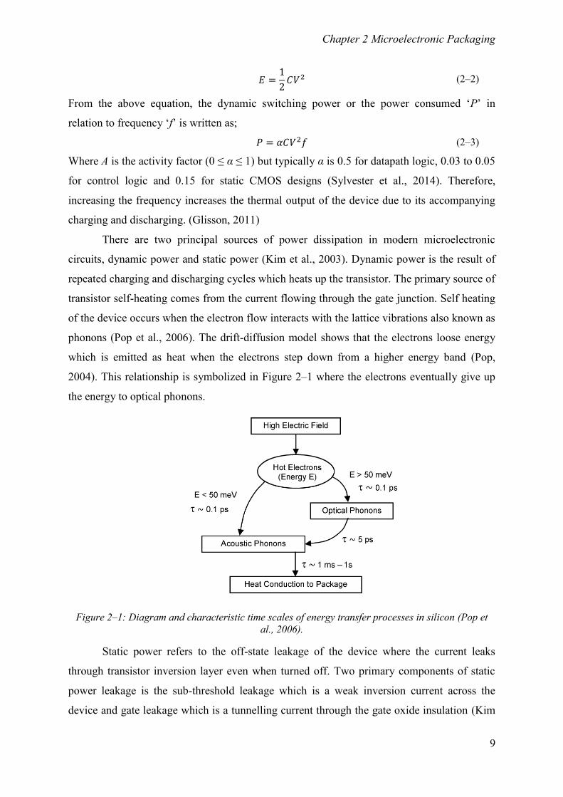
phonons (Pop et al., 2006). The drift-diffusion model shows that the electrons loose energy
which is emitted as heat when the electrons step down from a higher energy band (Pop,
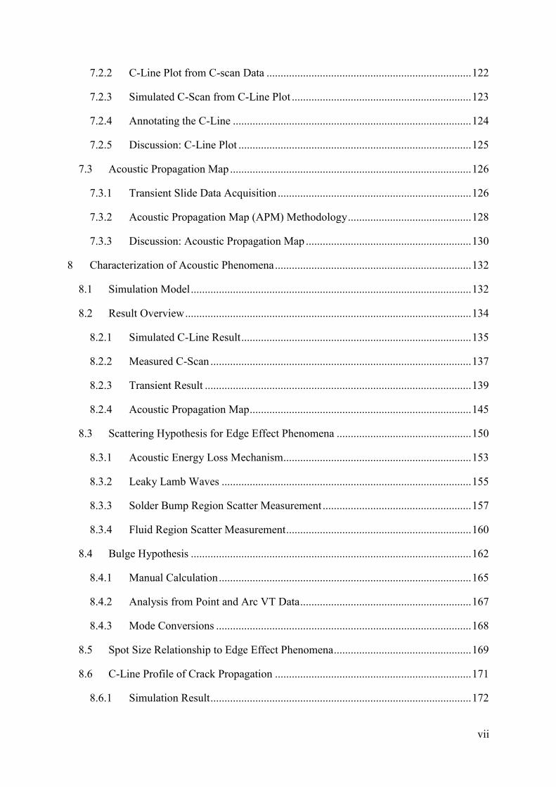
2004). This relationship is symbolized in Figure 2–1 where the electrons eventually give up
the energy to optical phonons.
Figure 2–1: Diagram and characteristic time scales of energy transfer processes in silicon (Pop et
al., 2006).
Static power refers to the off-state leakage of the device where the current leaks
through transistor inversion layer even when turned off. Two primary components of static
power leakage is the sub-threshold leakage which is a weak inversion current across the
device and gate leakage which is a tunnelling current through the gate oxide insulation (Kim
Chapter 2 Microelectronic Packaging
10
et al., 2003). Unlike dynamic power, static leakage is exacerbated by smaller device
geometries. For nano-scale devices, static power becomes significant. Hence equation 2–3 is
rewritten as;
(2–4)
Describing the total power dissipated as a sum of dynamic power and static power. The
second term models the static power loss due to the leakage current Ileak .
For decades, some engineers have grappled with the concept of heat dissipation
through erasure of information. Computation is an abstract mathematical process of mapping
the input bits into an output bit. Hence the question arises as Orlov puts it "Why would there
be any fundamental connection between such a mapping and the type of microscopic motion
we call heat?” (Orlov et al., 2012) The answer to the question requires a concept that
connects computational theory to the law of thermodynamics. Landauer's Principle describes
that since the computation is represented by physical systems, there will be fundamental heat
dissipation when the information is irreversibly erased (Landauer, 1961). This principle
postulates a new factor of heat dissipation which would affect devices with great processing
power. The Landauer Principle has recently been experimentally proven (Antoine et al.,
2012).
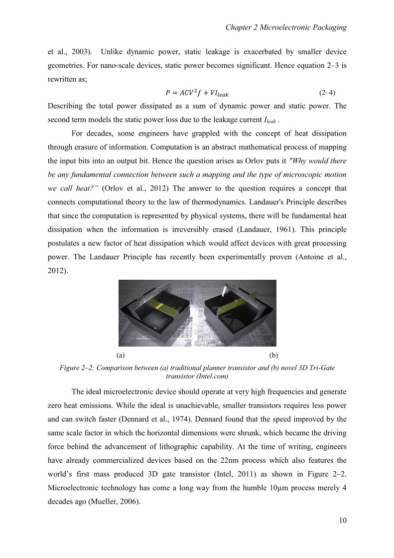
(a) (b)
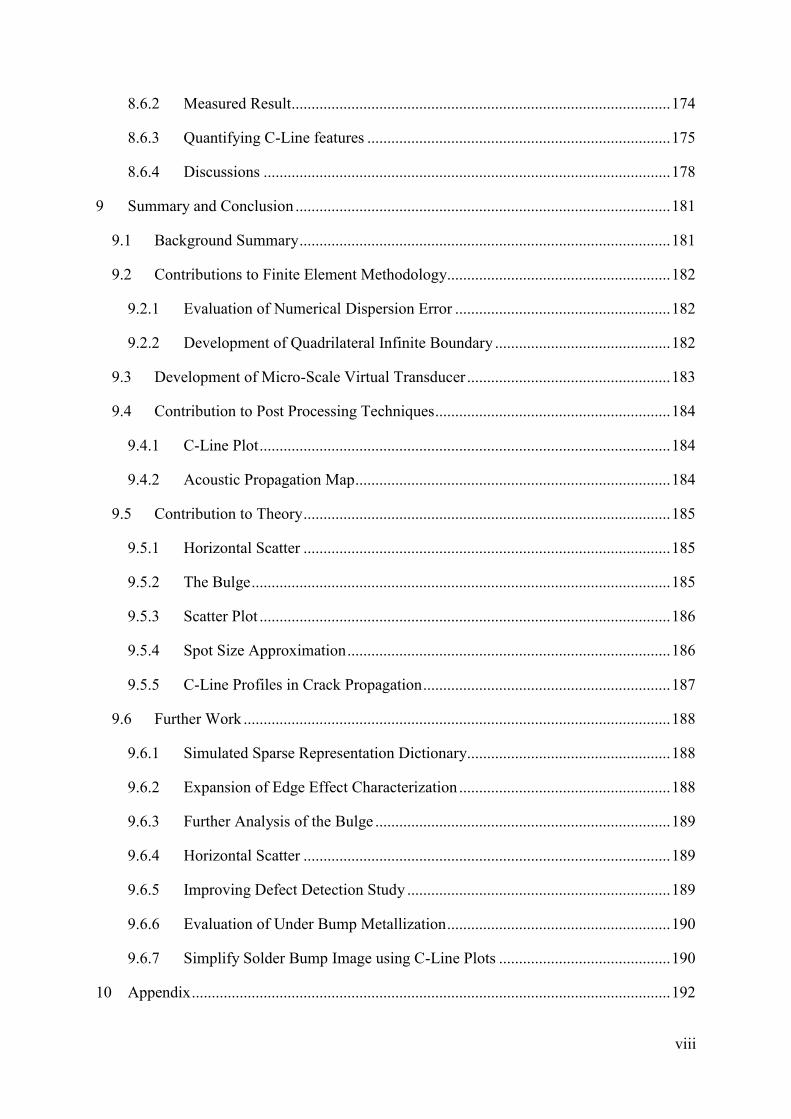
Figure 2–2: Comparison between (a) traditional planner transistor and (b) novel 3D Tri-Gate
transistor (Intel.com)
The ideal microelectronic device should operate at very high frequencies and generate
zero heat emissions. While the ideal is unachievable, smaller transistors requires less power
and can switch faster (Dennard et al., 1974). Dennard found that the speed improved by the
same scale factor in which the horizontal dimensions were shrunk, which became the driving
force behind the advancement of lithographic capability. At the time of writing, engineers
have already commercialized devices based on the 22nm process which also features the
world’s first mass produced 3D gate transistor (Intel, 2011) as shown in Figure 2–2.
Microelectronic technology has come a long way from the humble 10µm process merely 4
decades ago (Mueller, 2006).
Chapter 2 Microelectronic Packaging
11
2.2 Microelectronic Packaging
The field of electronic packaging is very wide encompassing materials science,
electronics, and manufacturing processes. The quality and precision of the package has to
keep pace with increasingly complex die configurations. Microelectronic packages are
required to accommodate increasing I/O channels while shrinking in overall size forcing
tighter and finer package I/O pitches. High operational frequencies require materials with
lower dielectric constants and losses. Increasing heat dissipation necessitates complex
cooling structures and improved interface materials. The shrinking die cannot function
without a compliant package to house it.
The basic roles of semiconductor packaging are to provide an encapsulated mounting
platform for the die whilst providing connections to the outside world. The packaging
mechanically protects the delicate die-system and allows physical handling both which are
critical for use in the manufacturing process (Braden, 2012). In operation, the packaging
provides thermal management as well as a physical interface to couple heat sinks for high
powered applications. There are two principle aspects to microelectronic packaging which is
the packaging technique and the mounting technology. The former concerns both the material
and technique used to mount and encapsulate the die while the latter focuses on providing
interconnects to the external environment as well as to other dies in new generation stacked
die technologies.
2.2.1 Ball Grid Array Packaging
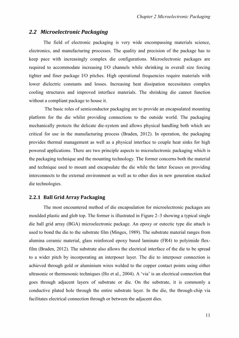
The most encountered method of die encapsulation for microelectronic packages are
moulded plastic and glob top. The former is illustrated in Figure 2–3 showing a typical single
die ball grid array (BGA) microelectronic package. An epoxy or eutectic type die attach is
used to bond the die to the substrate film (Minges, 1989). The substrate material ranges from
alumina ceramic material, glass reinforced epoxy based laminate (FR4) to polyimide flex-
film (Braden, 2012). The substrate also allows the electrical interface of the die to be spread
to a wider pitch by incorporating an interposer layer. The die to interposer connection is
achieved through gold or aluminium wires welded to the copper contact points using either
ultrasonic or thermosonic techniques (Ho et al., 2004). A ‘via’ is an electrical connection that
goes through adjacent layers of substrate or die. On the substrate, it is commonly a
conductive plated hole through the entire substrate layer. In the die, the through-chip via
facilitates electrical connection through or between the adjacent dies.
Chapter 2 Microelectronic Packaging
12
Die Attach
Mold Compound
Wire Bond
Substrate
Die
Solder
bump
Via
Circuit
Weld
Figure 2–3: Cross-section illustration of typical ball grid array packaging
2.2.2 Flip Chip Technology
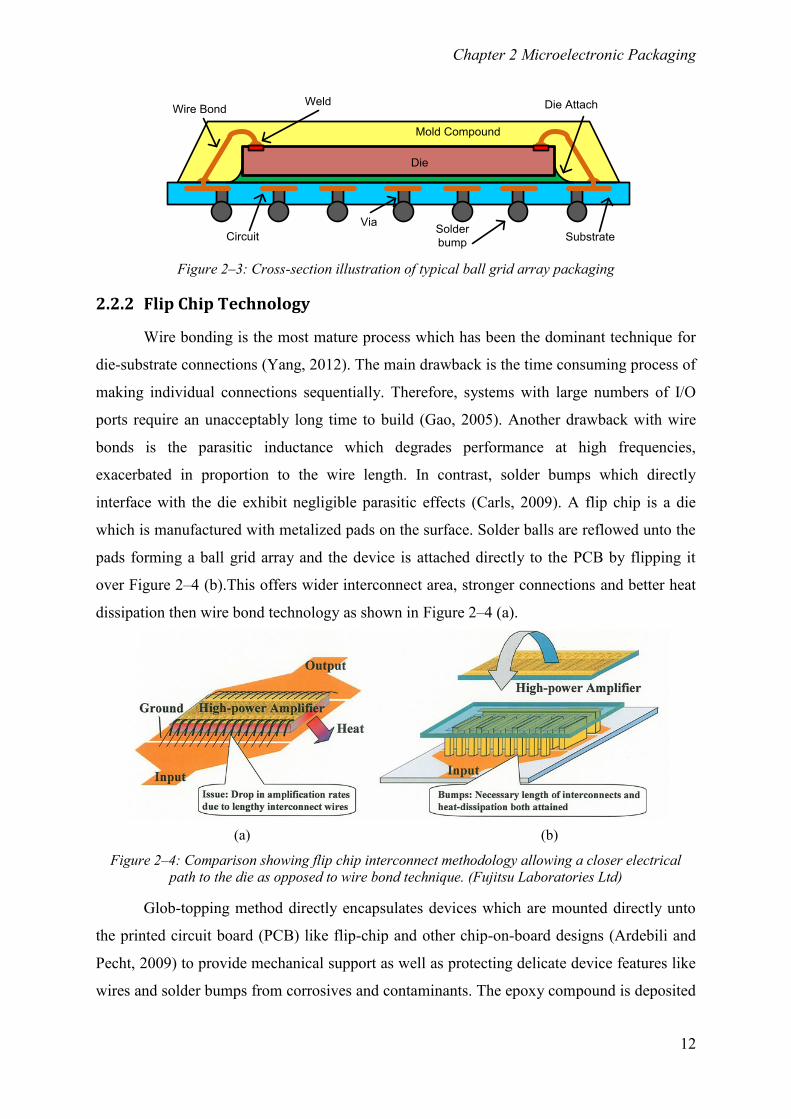
Wire bonding is the most mature process which has been the dominant technique for
die-substrate connections (Yang, 2012). The main drawback is the time consuming process of
making individual connections sequentially. Therefore, systems with large numbers of I/O
ports require an unacceptably long time to build (Gao, 2005). Another drawback with wire
bonds is the parasitic inductance which degrades performance at high frequencies,
exacerbated in proportion to the wire length. In contrast, solder bumps which directly
interface with the die exhibit negligible parasitic effects (Carls, 2009). A flip chip is a die
which is manufactured with metalized pads on the surface. Solder balls are reflowed unto the
pads forming a ball grid array and the device is attached directly to the PCB by flipping it
over Figure 2–4 (b).This offers wider interconnect area, stronger connections and better heat
dissipation then wire bond technology as shown in Figure 2–4 (a).
(a) (b)
Figure 2–4: Comparison showing flip chip interconnect methodology allowing a closer electrical
path to the die as opposed to wire bond technique. (Fujitsu Laboratories Ltd)
Glob-topping method directly encapsulates devices which are mounted directly unto
the printed circuit board (PCB) like flip-chip and other chip-on-board designs (Ardebili and
Pecht, 2009) to provide mechanical support as well as protecting delicate device features like
wires and solder bumps from corrosives and contaminants. The epoxy compound is deposited
Chapter 2 Microelectronic Packaging
13
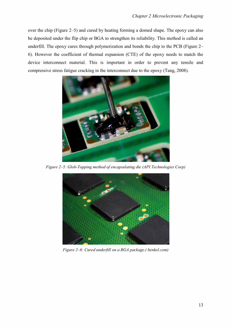
over the chip (Figure 2–5) and cured by heating forming a domed shape. The epoxy can also
be deposited under the flip chip or BGA to strengthen its reliability. This method is called an
underfill. The epoxy cures through polymerization and bonds the chip to the PCB (Figure 2–
6). However the coefficient of thermal expansion (CTE) of the epoxy needs to match the
device interconnect material. This is important in order to prevent any tensile and
compressive stress fatigue cracking in the interconnect due to the epoxy (Tang, 2008).
Figure 2–5: Glob-Topping method of encapsulating die (API Technologies Corp)
Figure 2–6: Cured underfill on a BGA package.( henkel.com)
Chapter 2 Microelectronic Packaging
14
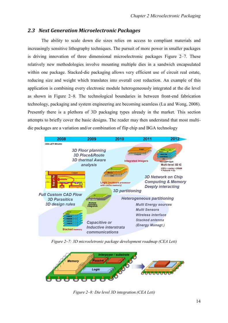
2.3 Next Generation Microelectronic Packages
The ability to scale down die sizes relies on access to compliant materials and
increasingly sensitive lithography techniques. The pursuit of more power in smaller packages
is driving innovation of three dimensional microelectronic packages Figure 2–7. These
relatively new methodologies involve mounting multiple dies in a sandwich encapsulated
within one package. Stacked-die packaging allows very efficient use of circuit real estate,
reducing size and weight which translates into overall cost reduction. An example of this
application is combining every electronic module heterogeneously integrated at the die level
as shown in Figure 2–8. The technological boundaries in between front-end fabrication
technology, packaging and system engineering are becoming seamless (Lu and Wong, 2008).
Presently there is a plethora of 3D packaging types already in the market. This section
attempts to briefly cover the basic designs. The reader may then understand that most multi-
die packages are a variation and/or combination of flip chip and BGA technology
Figure 2–7: 3D microeletronic package development roadmap (CEA Leti)
Figure 2–8: Die level 3D integration.(CEA Leti)
Chapter 2 Microelectronic Packaging
15
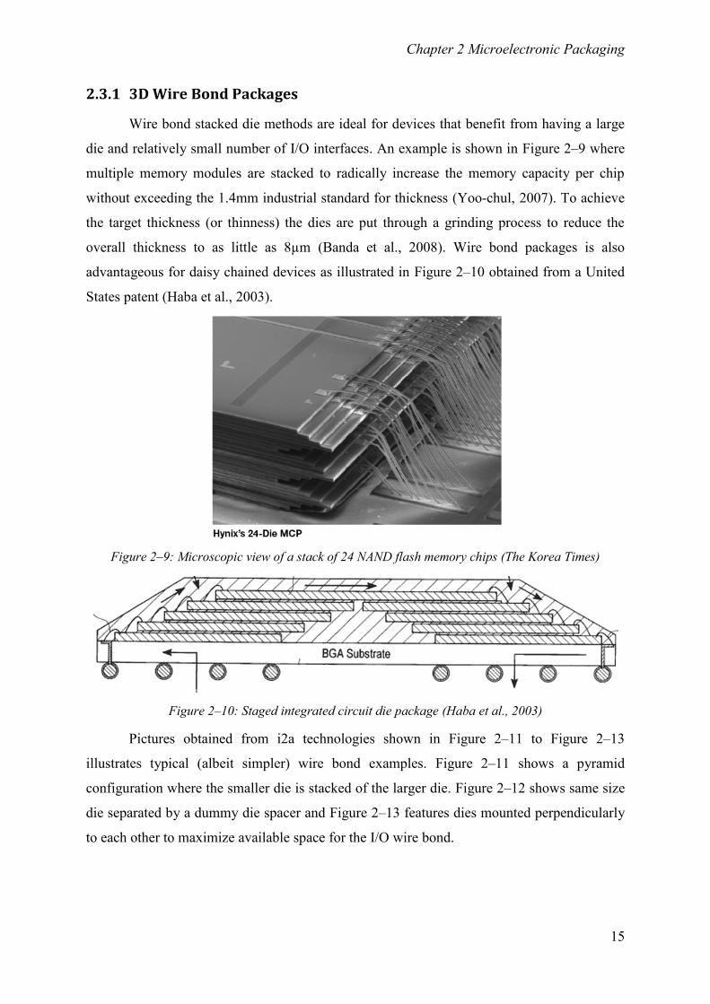
2.3.1 3D Wire Bond Packages
Wire bond stacked die methods are ideal for devices that benefit from having a large
die and relatively small number of I/O interfaces. An example is shown in Figure 2–9 where
multiple memory modules are stacked to radically increase the memory capacity per chip
without exceeding the 1.4mm industrial standard for thickness (Yoo-chul, 2007). To achieve
the target thickness (or thinness) the dies are put through a grinding process to reduce the
overall thickness to as little as 8µm (Banda et al., 2008). Wire bond packages is also
advantageous for daisy chained devices as illustrated in Figure 2–10 obtained from a United
States patent (Haba et al., 2003).
Figure 2–9: Microscopic view of a stack of 24 NAND flash memory chips (The Korea Times)
Figure 2–10: Staged integrated circuit die package (Haba et al., 2003)
Pictures obtained from i2a technologies shown in Figure 2–11 to Figure 2–13
illustrates typical (albeit simpler) wire bond examples. Figure 2–11 shows a pyramid
configuration where the smaller die is stacked of the larger die. Figure 2–12 shows same size
die separated by a dummy die spacer and Figure 2–13 features dies mounted perpendicularly
to each other to maximize available space for the I/O wire bond.
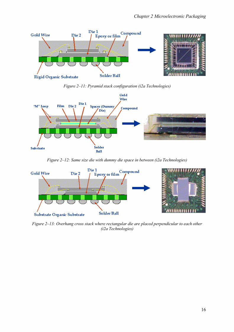
Chapter 2 Microelectronic Packaging
16
Figure 2–11: Pyramid stack configuration (i2a Technologies)
Figure 2–12: Same size die with dummy die space in between (i2a Technologies)
Figure 2–13: Overhang cross stack where rectangular die are placed perpendicular to each other
(i2a Technologies)
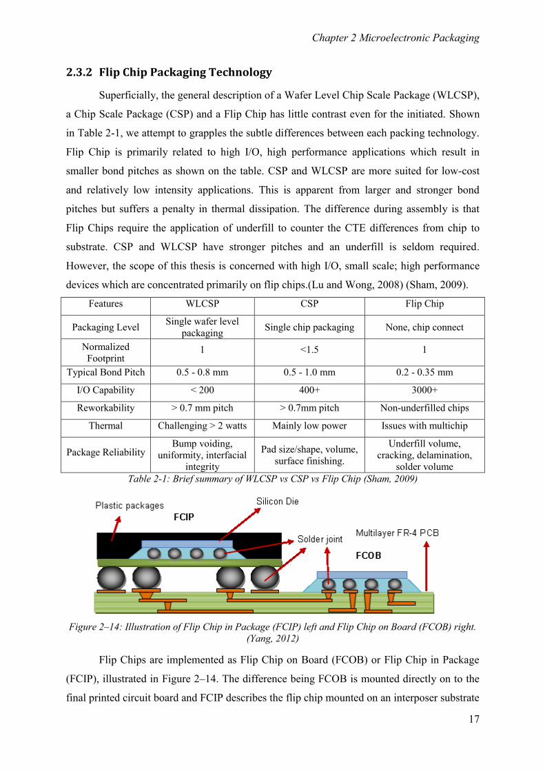
Chapter 2 Microelectronic Packaging
17
2.3.2 Flip Chip Packaging Technology
Superficially, the general description of a Wafer Level Chip Scale Package (WLCSP),
a Chip Scale Package (CSP) and a Flip Chip has little contrast even for the initiated. Shown
in Table 2-1, we attempt to grapples the subtle differences between each packing technology.
Flip Chip is primarily related to high I/O, high performance applications which result in
smaller bond pitches as shown on the table. CSP and WLCSP are more suited for low-cost
and relatively low intensity applications. This is apparent from larger and stronger bond
pitches but suffers a penalty in thermal dissipation. The difference during assembly is that
Flip Chips require the application of underfill to counter the CTE differences from chip to
substrate. CSP and WLCSP have stronger pitches and an underfill is seldom required.
However, the scope of this thesis is concerned with high I/O, small scale; high performance
devices which are concentrated primarily on flip chips.(Lu and Wong, 2008) (Sham, 2009).
Features WLCSP CSP Flip Chip
Packaging Level Single wafer level
packaging Single chip packaging None, chip connect
Normalized
Footprint 1 <1.5 1
Typical Bond Pitch 0.5 - 0.8 mm 0.5 - 1.0 mm 0.2 - 0.35 mm
I/O Capability < 200 400+ 3000+
Reworkability > 0.7 mm pitch > 0.7mm pitch Non-underfilled chips
Thermal Challenging > 2 watts Mainly low power Issues with multichip
Package Reliability Bump voiding,
uniformity, interfacial
integrity
Pad size/shape, volume,
surface finishing.
Underfill volume,
cracking, delamination,
solder volume
Table 2-1: Brief summary of WLCSP vs CSP vs Flip Chip (Sham, 2009)
Figure 2–14: Illustration of Flip Chip in Package (FCIP) left and Flip Chip on Board (FCOB) right.
(Yang, 2012)
Flip Chips are implemented as Flip Chip on Board (FCOB) or Flip Chip in Package
(FCIP), illustrated in Figure 2–14. The difference being FCOB is mounted directly on to the
final printed circuit board and FCIP describes the flip chip mounted on an interposer substrate
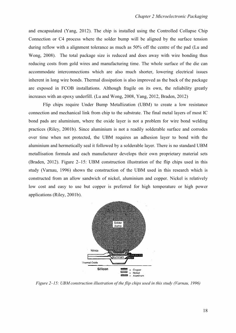
Chapter 2 Microelectronic Packaging
18
and encapsulated (Yang, 2012). The chip is installed using the Controlled Collapse Chip
Connection or C4 process where the solder bump will be aligned by the surface tension
during reflow with a alignment tolerance as much as 50% off the centre of the pad (Lu and
Wong, 2008). The total package size is reduced and does away with wire bonding thus
reducing costs from gold wires and manufacturing time. The whole surface of the die can
accommodate interconnections which are also much shorter, lowering electrical issues
inherent in long wire bonds. Thermal dissipation is also improved as the back of the package
are exposed in FCOB installations. Although fragile on its own, the reliability greatly
increases with an epoxy underfill. (Lu and Wong, 2008, Yang, 2012, Braden, 2012)
Flip chips require Under Bump Metallization (UBM) to create a low resistance
connection and mechanical link from chip to the substrate. The final metal layers of most IC
bond pads are aluminium, where the oxide layer is not a problem for wire bond welding
practices (Riley, 2001b). Since aluminium is not a readily solderable surface and corrodes
over time when not protected, the UBM requires an adhesion layer to bond with the
aluminium and hermetically seal it followed by a solderable layer. There is no standard UBM
metallisation formula and each manufacturer develops their own proprietary material sets
(Braden, 2012). Figure 2–15: UBM construction illustration of the flip chips used in this
study (Varnau, 1996) shows the construction of the UBM used in this research which is
constructed from an allow sandwich of nickel, aluminium and copper. Nickel is relatively
low cost and easy to use but copper is preferred for high temperature or high power
applications (Riley, 2001b).
Figure 2–15: UBM construction illustration of the flip chips used in this study (Varnau, 1996)
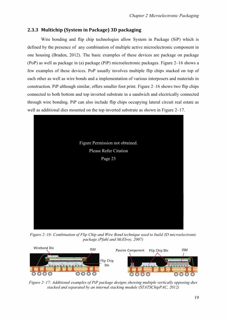
Chapter 2 Microelectronic Packaging
19
2.3.3 Multichip (System in Package) 3D packaging
Wire bonding and flip chip technologies allow System in Package (SiP) which is
defined by the presence of any combination of multiple active microelectronic component in
one housing (Braden, 2012). The basic examples of these devices are package on package
(PoP) as well as package in (a) package (PiP) microelectronic packages. Figure 2–16 shows a
few examples of these devices. PoP usually involves multiple flip chips stacked on top of
each other as well as wire bonds and a implementation of various interposers and materials in
construction. PiP although similar, offers smaller foot print. Figure 2–16 shows two flip chips
connected to both bottom and top inverted substrate in a sandwich and electrically connected
through wire bonding. PiP can also include flip chips occupying lateral circuit real estate as
well as additional dies mounted on the top inverted substrate as shown in Figure 2–17.
Figure 2–16: Combination of Flip Chip and Wire Bond technique used to build 3D microelectronic
package.(Pfahl and McElroy, 2007)
Figure 2–17: Additional examples of PiP package designs showing multiple vertically opposing dies
stacked and separated by an internal stacking module (STATSChipPAC, 2012)
Figure Permission not obtained.
Please Refer Citation
Page 25
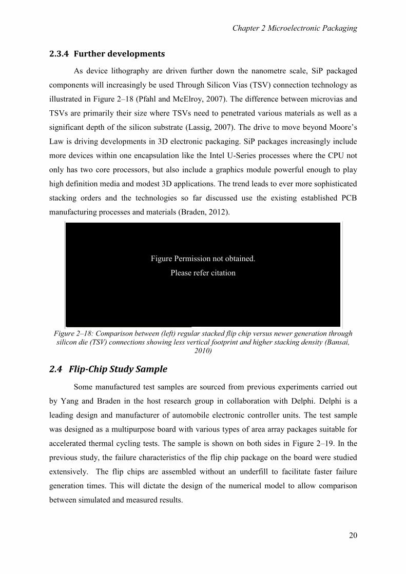
Chapter 2 Microelectronic Packaging
20
2.3.4 Further developments
As device lithography are driven further down the nanometre scale, SiP packaged
components will increasingly be used Through Silicon Vias (TSV) connection technology as
illustrated in Figure 2–18 (Pfahl and McElroy, 2007). The difference between microvias and
TSVs are primarily their size where TSVs need to penetrated various materials as well as a
significant depth of the silicon substrate (Lassig, 2007). The drive to move beyond Moore’s
Law is driving developments in 3D electronic packaging. SiP packages increasingly include
more devices within one encapsulation like the Intel U-Series processes where the CPU not
only has two core processors, but also include a graphics module powerful enough to play
high definition media and modest 3D applications. The trend leads to ever more sophisticated
stacking orders and the technologies so far discussed use the existing established PCB
manufacturing processes and materials (Braden, 2012).
Figure 2–18: Comparison between (left) regular stacked flip chip versus newer generation through
silicon die (TSV) connections showing less vertical footprint and higher stacking density (Bansai,
2010)
2.4 Flip-Chip Study Sample
Some manufactured test samples are sourced from previous experiments carried out
by Yang and Braden in the host research group in collaboration with Delphi. Delphi is a
leading design and manufacturer of automobile electronic controller units. The test sample
was designed as a multipurpose board with various types of area array packages suitable for
accelerated thermal cycling tests. The sample is shown on both sides in Figure 2–19. In the
previous study, the failure characteristics of the flip chip package on the board were studied
extensively. The flip chips are assembled without an underfill to facilitate faster failure
generation times. This will dictate the design of the numerical model to allow comparison
between simulated and measured results.
Figure Permission not obtained.
Please refer citation
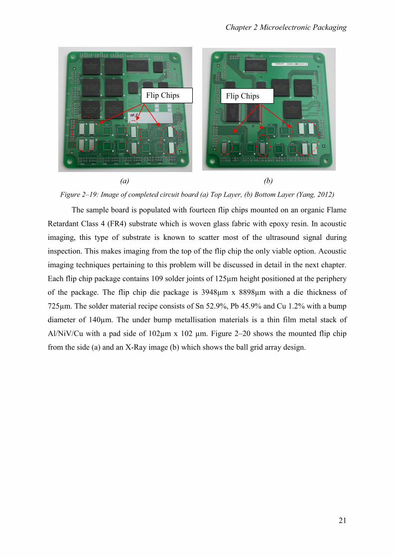
Chapter 2 Microelectronic Packaging
21
(a) (b)
Figure 2–19: Image of completed circuit board (a) Top Layer, (b) Bottom Layer (Yang, 2012)
The sample board is populated with fourteen flip chips mounted on an organic Flame
Retardant Class 4 (FR4) substrate which is woven glass fabric with epoxy resin. In acoustic
imaging, this type of substrate is known to scatter most of the ultrasound signal during
inspection. This makes imaging from the top of the flip chip the only viable option. Acoustic
imaging techniques pertaining to this problem will be discussed in detail in the next chapter.
Each flip chip package contains 109 solder joints of 125µm height positioned at the periphery
of the package. The flip chip die package is 3948µm x 8898µm with a die thickness of
725µm. The solder material recipe consists of Sn 52.9%, Pb 45.9% and Cu 1.2% with a bump
diameter of 140µm. The under bump metallisation materials is a thin film metal stack of
Al/NiV/Cu with a pad side of 102µm x 102 µm. Figure 2–20 shows the mounted flip chip
from the side (a) and an X-Ray image (b) which shows the ball grid array design.
Flip Chips Flip Chips
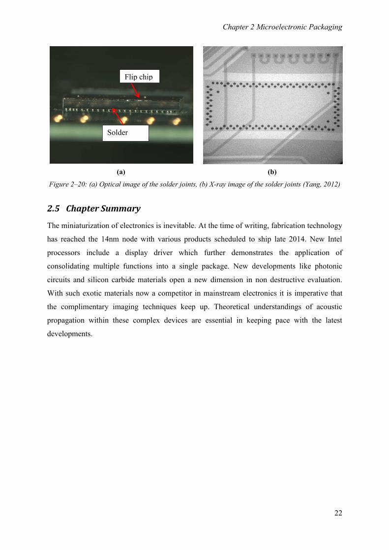
Chapter 2 Microelectronic Packaging
22
(a) (b)
Figure 2–20: (a) Optical image of the solder joints, (b) X-ray image of the solder joints (Yang, 2012)
2.5 Chapter Summary
The miniaturization of electronics is inevitable. At the time of writing, fabrication technology
has reached the 14nm node with various products scheduled to ship late 2014. New Intel
processors include a display driver which further demonstrates the application of
consolidating multiple functions into a single package. New developments like photonic
circuits and silicon carbide materials open a new dimension in non destructive evaluation.
With such exotic materials now a competitor in mainstream electronics it is imperative that
the complimentary imaging techniques keep up. Theoretical understandings of acoustic
propagation within these complex devices are essential in keeping pace with the latest
developments.
Flip chip
Solder
joints
Chapter 3 Acoustic Micro Imaging of Microelectronic Packages
23
Chapter 3
Acoustic Micro Imaging of
Microelectronic Packages
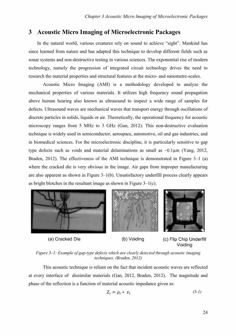
Chapter 3 Acoustic Micro Imaging of Microelectronic Packages
24
3 Acoustic Micro Imaging of Microelectronic Packages
In the natural world, various creatures rely on sound to achieve “sight”. Mankind has
since learned from nature and has adapted this technique to develop different fields such as
sonar systems and non-destructive testing in various sciences. The exponential rise of modern
technology, namely the progression of integrated circuit technology drives the need to
research the material properties and structural features at the micro- and nanometre-scales.
Acoustic Micro Imaging (AMI) is a methodology developed to analyze the
mechanical properties of various materials. It utilizes high frequency sound propagation
above human hearing also known as ultrasound to inspect a wide range of samples for
defects. Ultrasound waves are mechanical waves that transport energy through oscillations of
discrete particles in solids, liquids or air. Theoretically, the operational frequency for acoustic
microscopy ranges from 5 MHz to 3 GHz (Gan, 2012). This non-destructive evaluation
technique is widely used in semiconductor, aerospace, automotive, oil and gas industries, and
in biomedical sciences. For the microelectronic discipline, it is particularly sensitive to gap
type defects such as voids and material delaminations as small as ~0.1µm (Yang, 2012,
Braden, 2012). The effectiveness of the AMI technique is demonstrated in Figure 3–1 (a)
where the cracked die is very obvious in the image. Air gaps from improper manufacturing
are also apparent as shown in Figure 3–1(b). Unsatisfactory underfill process clearly appears
as bright blotches in the resultant image as shown in Figure 3–1(c).
Figure 3–1: Example of gap-type defects which are clearly detected through acoustic imaging
techniques. (Braden, 2012)
This acoustic technique is reliant on the fact that incident acoustic waves are reflected
at every interface of dissimilar materials (Gan, 2012, Braden, 2012). The magnitude and
phase of the reflection is a function of material acoustic impedance given as:
(3-1)
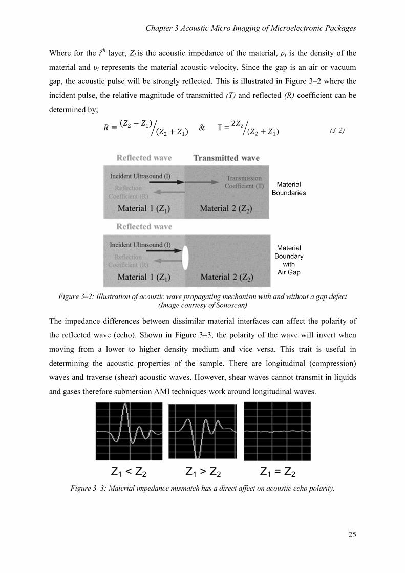
Chapter 3 Acoustic Micro Imaging of Microelectronic Packages
25
Where for the ith
layer, Zi is the acoustic impedance of the material, ρi is the density of the
material and υi represents the material acoustic velocity. Since the gap is an air or vacuum
gap, the acoustic pulse will be strongly reflected. This is illustrated in Figure 3–2 where the
incident pulse, the relative magnitude of transmitted (T) and reflected (R) coefficient can be
determined by;
& T =
(3-2)
Figure 3–2: Illustration of acoustic wave propagating mechanism with and without a gap defect
(Image courtesy of Sonoscan)
The impedance differences between dissimilar material interfaces can affect the polarity of
the reflected wave (echo). Shown in Figure 3–3, the polarity of the wave will invert when
moving from a lower to higher density medium and vice versa. This trait is useful in
determining the acoustic properties of the sample. There are longitudinal (compression)
waves and traverse (shear) acoustic waves. However, shear waves cannot transmit in liquids
and gases therefore submersion AMI techniques work around longitudinal waves.
Figure 3–3: Material impedance mismatch has a direct affect on acoustic echo polarity.
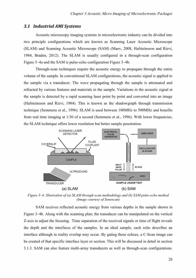
Chapter 3 Acoustic Micro Imaging of Microelectronic Packages
26
3.1 Industrial AMI Systems
Acoustic microscopy imaging systems in microelectronic industry can be divided into
two principle configurations which are known as Scanning Laser Acoustic Microscope
(SLAM) and Scanning Acoustic Microscope (SAM) (Maev, 2008, Hafsteinsson and Rizvi,
1984, Braden, 2012). The SLAM is usually configured in a through-scan configuration
Figure 3–4a and the SAM is pulse-echo configuration Figure 3–4b.
Through-scan techniques require the acoustic energy to propagate through the entire
volume of the sample. In conventional SLAM configurations, the acoustic signal is applied to
the sample via a transducer. The wave propagating through the sample is attenuated and
refracted by various features and materials in the sample. Variations in the acoustic signal at
the sample is detected by a rapid scanning laser point by point and converted into an image
(Hafsteinsson and Rizvi, 1984). This is known as the shadowgraph through transmission
technique (Semmens et al., 1996). SLAM is used between 100MHz to 500MHz and benefits
from real time imaging at 1/30 of a second (Semmens et al., 1996). With lower frequencies,
the SLAM technique offers lower resolution but better sample penetration.
Figure 3–4: Illustration of (a) SLAM through-scan methodology and (b) SAM pulse-echo method
(Image courtesy of Sonoscan)
SAM receives reflected acoustic energy from various depths in the sample shown in
Figure 3–4b. Along with the scanning plan; the transducer can be manipulated on the vertical
Z-axis to adjust the focusing. Time separation of the received signals or time of flight reveals
the depth and the interfaces of the samples. In an ideal sample, each echo describes an
interface although in reality overlap may occur. By gating these echoes, a C-Scan image can
be created of that specific interface layer or section. This will be discussed in detail in section
3.1.3. SAM can also feature multi-array transducers as well as through-scan configurations.
Chapter 3 Acoustic Micro Imaging of Microelectronic Packages
27
SAM can implement significantly wider and higher frequencies ranges up to the gigahertz
region (Gan, 2012).
SLAM is not to be confused with the techniques of Laser Ultrasonics. This method
uses lasers to form acoustic waves by means of ablation or thermoelastic mechanisms (Dixon,
2006). The ablation regime will either vaporize the sample surface or break down the air
which the shockwave generates an acoustic response (Stauter et al., 1997, Hopko and Ume,
1999) on the sample. The thermoelastic regime heats the sample which causes a mechanical
expansion. With repeated laser pulses, this thermal expansion or repeated ablation generates
an acoustic response (Kim et al., 1998). Detection of the acoustic response falls into two
categories which are interferometric detection (vibrometers, time delay, etc) and amplitude
variation detection (knife edge) (Dixon 2006). Knife edge detectors are difficult to measure
exact wave amplitudes or waveform shapes but benefits from easier implementation, cost and
automation. There are many approaches with interferometry detectors. To generalize, this
detection method can be highly sensitive with high bandwidth and works on rough surfaces
(Dixon, 2006). This technique has a small footprint and is noncontact. Very high frequencies
associated to this technique limits useful measurement range to reasonably thin films
(Krishnaswamy, 2003). However electronics are packaged into increasingly thin sub
millimetre form factors. This technique may be significant in the future.
3.1.1 Frequency Dependant Attenuation
Using higher frequency transducers can increase the imaging resolution. However, the
acoustic energy is unable to penetrate the volume of the sample. In Newtonian fluids, the rate
of frequency dependent attenuation α is described by Stoke’ law of sound attenuation
(Dukhin and Goetz, 2010) which is written as equation (3-3),
(3-3)
where η is the dynamic viscosity coefficient of the fluid, ω is the frequency, ρ is the fluid
density and V is the acoustic velocity in the medium. However, the mathematical descriptions
for attenuation in solids are diverse (Jarvis and Bacon, 2005). This is due to the variety of
crystalline structures of the material which influences the effects of scattering and absorption
(Nagy, 2013). Therefore, reliable attenuation values are obtained experimentally for specific
materials (NDT, 2013a).
(3-4)
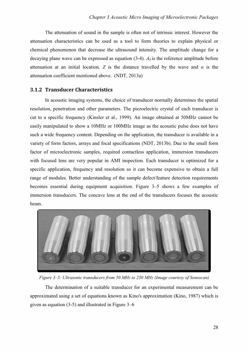
Chapter 3 Acoustic Micro Imaging of Microelectronic Packages
28
The attenuation of sound in the sample is often not of intrinsic interest. However the
attenuation characteristics can be used as a tool to form theories to explain physical or
chemical phenomenon that decrease the ultrasound intensity. The amplitude change for a
decaying plane wave can be expressed as equation (3-4). A0 is the reference amplitude before
attenuation at an initial location. Z is the distance travelled by the wave and α is the
attenuation coefficient mentioned above. (NDT, 2013a)
3.1.2 Transducer Characteristics
In acoustic imaging systems, the choice of transducer normally determines the spatial
resolution, penetration and other parameters. The piezoelectric crystal of each transducer is
cut to a specific frequency (Kinsler et al., 1999). An image obtained at 50MHz cannot be
easily manipulated to show a 10MHz or 100MHz image as the acoustic pulse does not have
such a wide frequency content. Depending on the application, the transducer is available in a
variety of form factors, arrays and focal specifications (NDT, 2013b). Due to the small form
factor of microelectronic samples, required contactless application, immersion transducers
with focused lens are very popular in AMI inspection. Each transducer is optimized for a
specific application, frequency and resolution so it can become expensive to obtain a full
range of modules. Better understanding of the sample defect/feature detection requirements
becomes essential during equipment acquisition. Figure 3–5 shows a few examples of
immersion transducers. The concave lens at the end of the transducers focuses the acoustic
beam.
Figure 3–5: Ultrasonic transducers from 50 MHz to 230 MHz (Image courtesy of Sonoscan)
The determination of a suitable transducer for an experimental measurement can be
approximated using a set of equations known as Kino's approximation (Kino, 1987) which is
given as equation (3-5) and illustrated in Figure 3–6
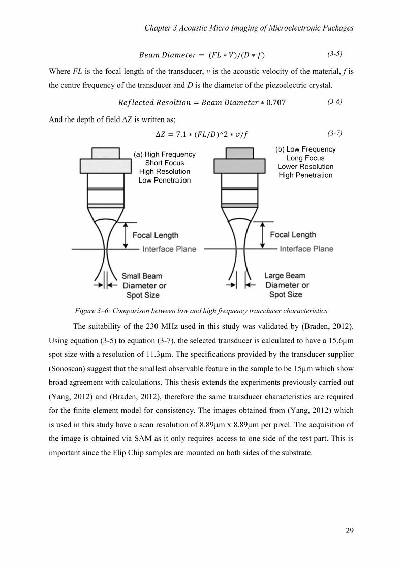
Chapter 3 Acoustic Micro Imaging of Microelectronic Packages
29
(3-5)
Where FL is the focal length of the transducer, v is the acoustic velocity of the material, f is
the centre frequency of the transducer and D is the diameter of the piezoelectric crystal.
(3-6)
And the depth of field ∆Z is written as;
(3-7)
Figure 3–6: Comparison between low and high frequency transducer characteristics
The suitability of the 230 MHz used in this study was validated by (Braden, 2012).
Using equation (3-5) to equation (3-7), the selected transducer is calculated to have a 15.6µm
spot size with a resolution of 11.3µm. The specifications provided by the transducer supplier
(Sonoscan) suggest that the smallest observable feature in the sample to be 15µm which show
broad agreement with calculations. This thesis extends the experiments previously carried out
(Yang, 2012) and (Braden, 2012), therefore the same transducer characteristics are required
for the finite element model for consistency. The images obtained from (Yang, 2012) which
is used in this study have a scan resolution of 8.89µm x 8.89µm per pixel. The acquisition of
the image is obtained via SAM as it only requires access to one side of the test part. This is
important since the Flip Chip samples are mounted on both sides of the substrate.
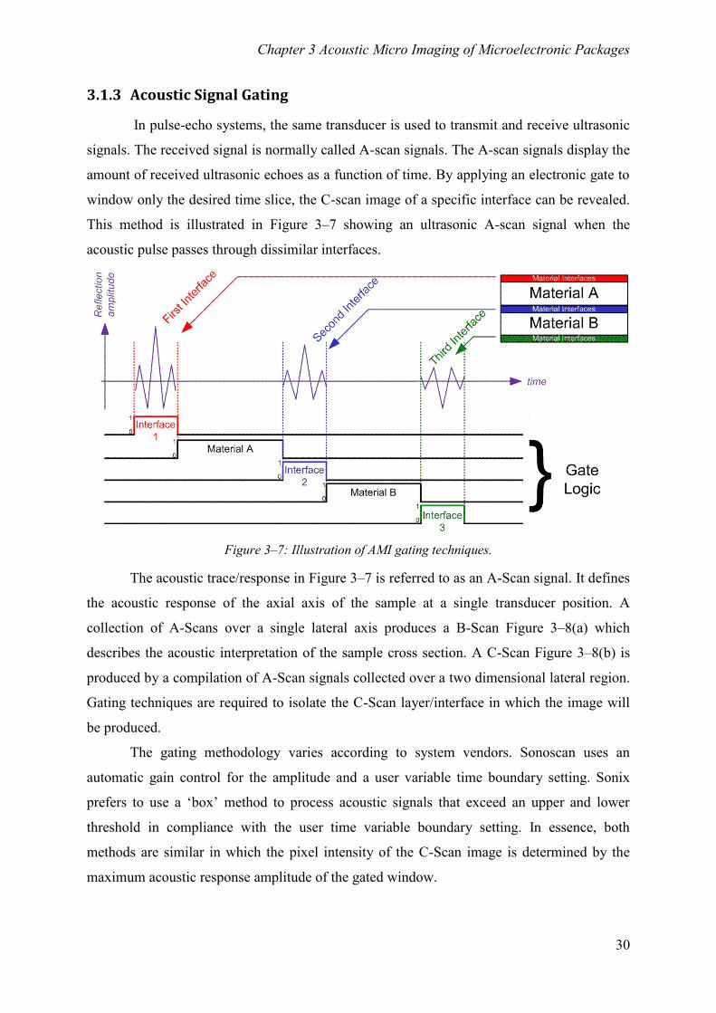
Chapter 3 Acoustic Micro Imaging of Microelectronic Packages
30
3.1.3 Acoustic Signal Gating
In pulse-echo systems, the same transducer is used to transmit and receive ultrasonic
signals. The received signal is normally called A-scan signals. The A-scan signals display the
amount of received ultrasonic echoes as a function of time. By applying an electronic gate to
window only the desired time slice, the C-scan image of a specific interface can be revealed.
This method is illustrated in Figure 3–7 showing an ultrasonic A-scan signal when the
acoustic pulse passes through dissimilar interfaces.
Figure 3–7: Illustration of AMI gating techniques.
The acoustic trace/response in Figure 3–7 is referred to as an A-Scan signal. It defines
the acoustic response of the axial axis of the sample at a single transducer position. A
collection of A-Scans over a single lateral axis produces a B-Scan Figure 3–8(a) which
describes the acoustic interpretation of the sample cross section. A C-Scan Figure 3–8(b) is
produced by a compilation of A-Scan signals collected over a two dimensional lateral region.
Gating techniques are required to isolate the C-Scan layer/interface in which the image will
be produced.
The gating methodology varies according to system vendors. Sonoscan uses an
automatic gain control for the amplitude and a user variable time boundary setting. Sonix
prefers to use a ‘box’ method to process acoustic signals that exceed an upper and lower
threshold in compliance with the user time variable boundary setting. In essence, both
methods are similar in which the pixel intensity of the C-Scan image is determined by the
maximum acoustic response amplitude of the gated window.
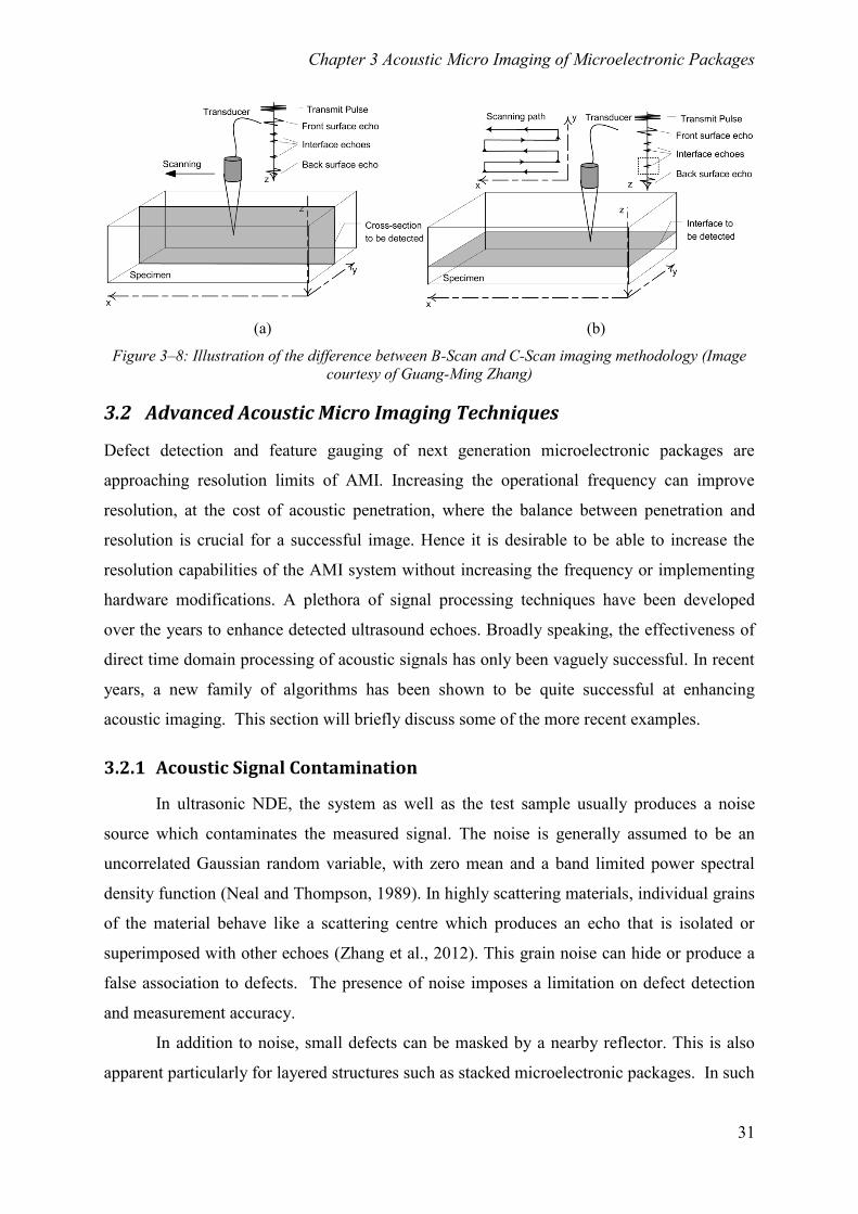
Chapter 3 Acoustic Micro Imaging of Microelectronic Packages
31
(a) (b)
Figure 3–8: Illustration of the difference between B-Scan and C-Scan imaging methodology (Image
courtesy of Guang-Ming Zhang)
3.2 Advanced Acoustic Micro Imaging Techniques
Defect detection and feature gauging of next generation microelectronic packages are
approaching resolution limits of AMI. Increasing the operational frequency can improve
resolution, at the cost of acoustic penetration, where the balance between penetration and
resolution is crucial for a successful image. Hence it is desirable to be able to increase the
resolution capabilities of the AMI system without increasing the frequency or implementing
hardware modifications. A plethora of signal processing techniques have been developed
over the years to enhance detected ultrasound echoes. Broadly speaking, the effectiveness of
direct time domain processing of acoustic signals has only been vaguely successful. In recent
years, a new family of algorithms has been shown to be quite successful at enhancing
acoustic imaging. This section will briefly discuss some of the more recent examples.
3.2.1 Acoustic Signal Contamination
In ultrasonic NDE, the system as well as the test sample usually produces a noise
source which contaminates the measured signal. The noise is generally assumed to be an
uncorrelated Gaussian random variable, with zero mean and a band limited power spectral
density function (Neal and Thompson, 1989). In highly scattering materials, individual grains
of the material behave like a scattering centre which produces an echo that is isolated or
superimposed with other echoes (Zhang et al., 2012). This grain noise can hide or produce a
false association to defects. The presence of noise imposes a limitation on defect detection
and measurement accuracy.
In addition to noise, small defects can be masked by a nearby reflector. This is also
apparent particularly for layered structures such as stacked microelectronic packages. In such
Chapter 3 Acoustic Micro Imaging of Microelectronic Packages
32
cases, the thicknesses of individual layers are comparable to the ultrasound wavelength which
leads to the overlapping between the front and back interface reflections. To improve the
acoustic signal without increasing frequency, a family of signal processing techniques such as
deconvolution (Yamani et al., 1997), sparse signal representation (Zhang et al., 2012), edge
detection (Murphy, 1991), and anisotropic or bilateral filtering (Ali et al., 2008) are
introduced. However, in acoustic flaw detection, the ultrasonic signal is usually a time and
frequency limited transient signal. Hence, time–frequency analysis techniques, are more
appropriate to process ultrasonic signals (Zhang et al., 2012).
3.2.2 Sparse Signal Representation
As part of the ongoing signal processing research by the host research group
spearheaded by Guang-Ming Zhang. Advanced sparse signal representation (SSR) algorithms
have been developed and published over a period of more than ten years. This approach has
been successfully applied to the problem of blind source separation (Zibulevsky and
Pearlmutter, 2001) and has been gaining popularity over the recent years. Blind source
separation refers to the extraction of signals which are not directly accessible where the
extraction is carried out from another set of measurements which were generated as mixtures
of the original set (Zarzoso and Nandi, 1999). SSR usually offers better performance and
efficient signal modelling compared to methods based on orthonormal transforms and direct
time domain processing (Huang and Aviyente, 2006). Generally, the activity of SSR
concentrates around two general problems; the algorithms for performing sparse
decomposition and the dictionary composition method (Aharon, 2006).
Using SSR, the time and frequency localization are preserved and have greater
robustness in the presence of noise as well as better flexibility in matching echo components
from the acoustic signal. In principle, the noisy and/or overlapping ultrasound echo is
decomposed into sparse representations over an overcomplete dictionary. This allows the
signal to be de-noised effectively and overlapping information can be isolated. The desired
isolated elements can then reconstructed through an approximation algorithm into a time
domain signal with the subsequent conventional acoustic image.
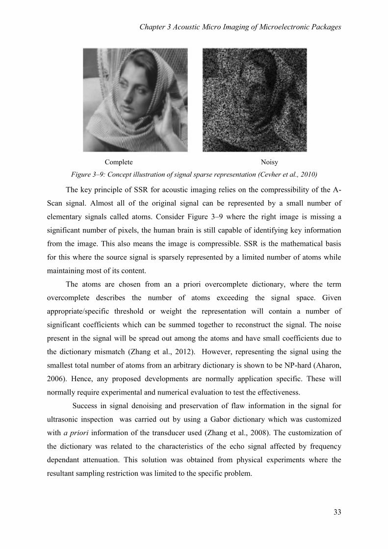
Chapter 3 Acoustic Micro Imaging of Microelectronic Packages
33
Complete Noisy
Figure 3–9: Concept illustration of signal sparse representation (Cevher et al., 2010)
The key principle of SSR for acoustic imaging relies on the compressibility of the A-
Scan signal. Almost all of the original signal can be represented by a small number of
elementary signals called atoms. Consider Figure 3–9 where the right image is missing a
significant number of pixels, the human brain is still capable of identifying key information
from the image. This also means the image is compressible. SSR is the mathematical basis
for this where the source signal is sparsely represented by a limited number of atoms while
maintaining most of its content.
The atoms are chosen from an a priori overcomplete dictionary, where the term
overcomplete describes the number of atoms exceeding the signal space. Given
appropriate/specific threshold or weight the representation will contain a number of
significant coefficients which can be summed together to reconstruct the signal. The noise
present in the signal will be spread out among the atoms and have small coefficients due to
the dictionary mismatch (Zhang et al., 2012). However, representing the signal using the
smallest total number of atoms from an arbitrary dictionary is shown to be NP-hard (Aharon,
2006). Hence, any proposed developments are normally application specific. These will
normally require experimental and numerical evaluation to test the effectiveness.
Success in signal denoising and preservation of flaw information in the signal for
ultrasonic inspection was carried out by using a Gabor dictionary which was customized
with a priori information of the transducer used (Zhang et al., 2008). The customization of
the dictionary was related to the characteristics of the echo signal affected by frequency
dependant attenuation. This solution was obtained from physical experiments where the
resultant sampling restriction was limited to the specific problem.
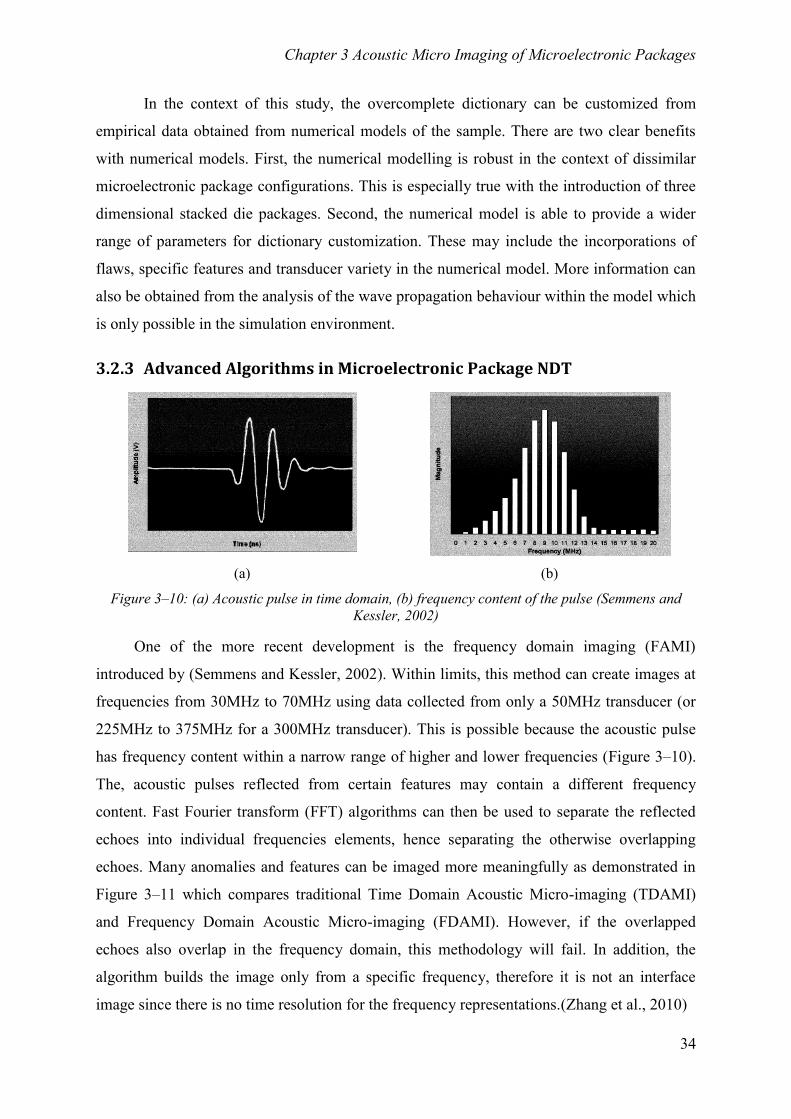
Chapter 3 Acoustic Micro Imaging of Microelectronic Packages
34
In the context of this study, the overcomplete dictionary can be customized from
empirical data obtained from numerical models of the sample. There are two clear benefits
with numerical models. First, the numerical modelling is robust in the context of dissimilar
microelectronic package configurations. This is especially true with the introduction of three
dimensional stacked die packages. Second, the numerical model is able to provide a wider
range of parameters for dictionary customization. These may include the incorporations of
flaws, specific features and transducer variety in the numerical model. More information can
also be obtained from the analysis of the wave propagation behaviour within the model which
is only possible in the simulation environment.
3.2.3 Advanced Algorithms in Microelectronic Package NDT
(a) (b)
Figure 3–10: (a) Acoustic pulse in time domain, (b) frequency content of the pulse (Semmens and
Kessler, 2002)
One of the more recent development is the frequency domain imaging (FAMI)
introduced by (Semmens and Kessler, 2002). Within limits, this method can create images at
frequencies from 30MHz to 70MHz using data collected from only a 50MHz transducer (or
225MHz to 375MHz for a 300MHz transducer). This is possible because the acoustic pulse
has frequency content within a narrow range of higher and lower frequencies (Figure 3–10).
The, acoustic pulses reflected from certain features may contain a different frequency
content. Fast Fourier transform (FFT) algorithms can then be used to separate the reflected
echoes into individual frequencies elements, hence separating the otherwise overlapping
echoes. Many anomalies and features can be imaged more meaningfully as demonstrated in
Figure 3–11 which compares traditional Time Domain Acoustic Micro-imaging (TDAMI)
and Frequency Domain Acoustic Micro-imaging (FDAMI). However, if the overlapped
echoes also overlap in the frequency domain, this methodology will fail. In addition, the
algorithm builds the image only from a specific frequency, therefore it is not an interface
image since there is no time resolution for the frequency representations.(Zhang et al., 2010)
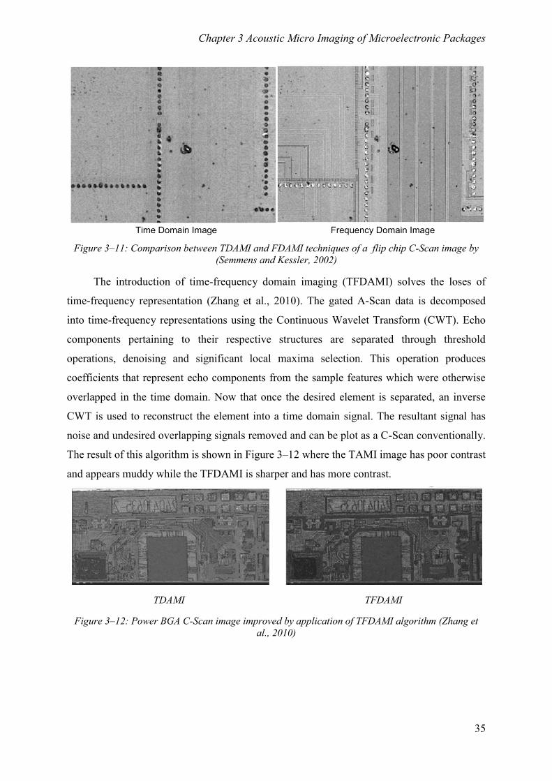
Chapter 3 Acoustic Micro Imaging of Microelectronic Packages
35
Figure 3–11: Comparison between TDAMI and FDAMI techniques of a flip chip C-Scan image by
(Semmens and Kessler, 2002)
The introduction of time-frequency domain imaging (TFDAMI) solves the loses of
time-frequency representation (Zhang et al., 2010). The gated A-Scan data is decomposed
into time-frequency representations using the Continuous Wavelet Transform (CWT). Echo
components pertaining to their respective structures are separated through threshold
operations, denoising and significant local maxima selection. This operation produces
coefficients that represent echo components from the sample features which were otherwise
overlapped in the time domain. Now that once the desired element is separated, an inverse
CWT is used to reconstruct the element into a time domain signal. The resultant signal has
noise and undesired overlapping signals removed and can be plot as a C-Scan conventionally.
The result of this algorithm is shown in Figure 3–12 where the TAMI image has poor contrast
and appears muddy while the TFDAMI is sharper and has more contrast.
TDAMI TFDAMI
Figure 3–12: Power BGA C-Scan image improved by application of TFDAMI algorithm (Zhang et
al., 2010)
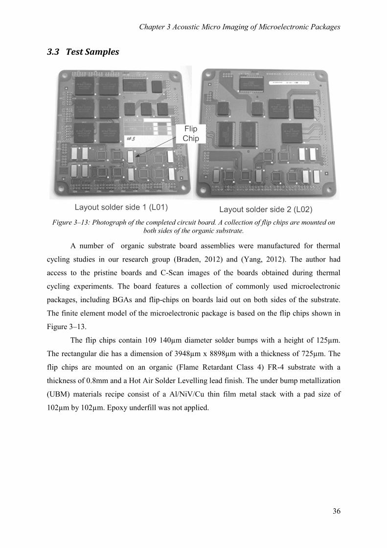
Chapter 3 Acoustic Micro Imaging of Microelectronic Packages
36
3.3 Test Samples
Figure 3–13: Photograph of the completed circuit board. A collection of flip chips are mounted on
both sides of the organic substrate.
A number of organic substrate board assemblies were manufactured for thermal
cycling studies in our research group (Braden, 2012) and (Yang, 2012). The author had
access to the pristine boards and C-Scan images of the boards obtained during thermal
cycling experiments. The board features a collection of commonly used microelectronic
packages, including BGAs and flip-chips on boards laid out on both sides of the substrate.
The finite element model of the microelectronic package is based on the flip chips shown in
Figure 3–13.
The flip chips contain 109 140µm diameter solder bumps with a height of 125µm.
The rectangular die has a dimension of 3948µm x 8898µm with a thickness of 725µm. The
flip chips are mounted on an organic (Flame Retardant Class 4) FR-4 substrate with a
thickness of 0.8mm and a Hot Air Solder Levelling lead finish. The under bump metallization
(UBM) materials recipe consist of a Al/NiV/Cu thin film metal stack with a pad size of
102µm by 102µm. Epoxy underfill was not applied.
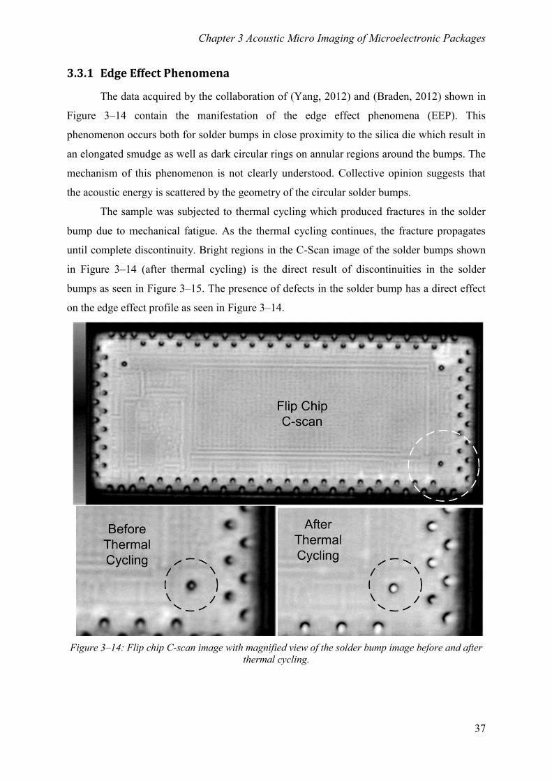
Chapter 3 Acoustic Micro Imaging of Microelectronic Packages
37
3.3.1 Edge Effect Phenomena
The data acquired by the collaboration of (Yang, 2012) and (Braden, 2012) shown in
Figure 3–14 contain the manifestation of the edge effect phenomena (EEP). This
phenomenon occurs both for solder bumps in close proximity to the silica die which result in
an elongated smudge as well as dark circular rings on annular regions around the bumps. The
mechanism of this phenomenon is not clearly understood. Collective opinion suggests that
the acoustic energy is scattered by the geometry of the circular solder bumps.
The sample was subjected to thermal cycling which produced fractures in the solder
bump due to mechanical fatigue. As the thermal cycling continues, the fracture propagates
until complete discontinuity. Bright regions in the C-Scan image of the solder bumps shown
in Figure 3–14 (after thermal cycling) is the direct result of discontinuities in the solder
bumps as seen in Figure 3–15. The presence of defects in the solder bump has a direct effect
on the edge effect profile as seen in Figure 3–14.
Figure 3–14: Flip chip C-scan image with magnified view of the solder bump image before and after
thermal cycling.
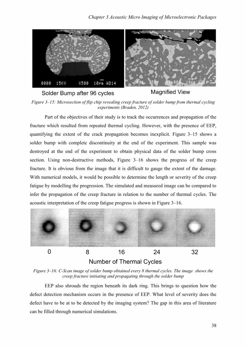
Chapter 3 Acoustic Micro Imaging of Microelectronic Packages
38
Figure 3–15: Microsection of flip chip revealing creep fracture of solder bump from thermal cycling
experiments (Braden, 2012)
Part of the objectives of their study is to track the occurrences and propagation of the
fracture which resulted from repeated thermal cycling. However, with the presence of EEP,
quantifying the extent of the crack propagation becomes inexplicit. Figure 3–15 shows a
solder bump with complete discontinuity at the end of the experiment. This sample was
destroyed at the end of the experiment to obtain physical data of the solder bump cross
section. Using non-destructive methods, Figure 3–16 shows the progress of the creep
fracture. It is obvious from the image that it is difficult to gauge the extent of the damage.
With numerical models, it would be possible to determine the length or severity of the creep
fatigue by modelling the progression. The simulated and measured image can be compared to
infer the propagation of the creep fracture in relation to the number of thermal cycles. The
acoustic interpretation of the creep fatigue progress is shown in Figure 3–16.
Figure 3–16: C-Scan image of solder bump obtained every 8 thermal cycles. The image shows the
creep fracture initiating and propagating through the solder bump
EEP also shrouds the region beneath its dark ring. This brings to question how the
defect detection mechanism occurs in the presence of EEP. What level of severity does the
defect have to be at to be detected by the imaging system? The gap in this area of literature
can be filled through numerical simulations.
Chapter 3 Acoustic Micro Imaging of Microelectronic Packages
39
3.4 Chapter Summary
This chapter features several examples of powerful algorithms and techniques employed to
maximize the potential of AMI. However, these techniques also demonstrate a lack of interest
on intra-sample acoustic mechanisms. While fundamental acoustic mechanisms are well
understood, layered and complex structures, some made from exotic materials or composites
complicates the defect detection mechanism. This limitation is largely due to the discreet
nature of the samples themselves. It is a major challenge to provide a general guidance that
applies to all samples. Inevitably, interpretation of acoustic imagines is guided by experience.
This raises a natural prerogative to study the theoretical aspects of the acoustic defect
detection mechanism specific to microelectronic packages. A theoretical guidance can
explain the manifestation of various image features, creating new post processing techniques
and characterize physical effects such as the edge effect phenomena. An innate understanding
of intra sample acoustic mechanisms also advises design decisions to allow easy detection of
critical failures.
Chapter 4 Acoustic Simulation by Finite Element Modelling
40
Chapter 4
Acoustic Simulation by Finite
Element Modelling
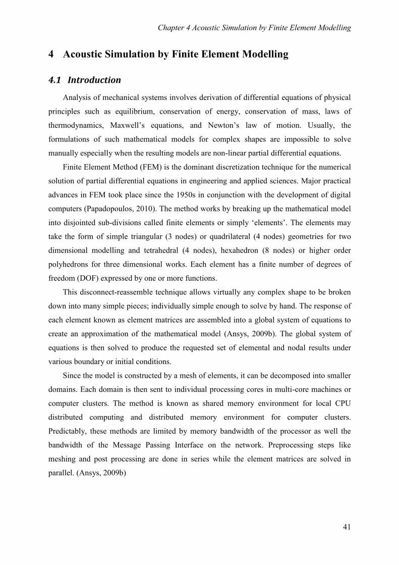
Chapter 4 Acoustic Simulation by Finite Element Modelling
41
4 Acoustic Simulation by Finite Element Modelling
4.1 Introduction
Analysis of mechanical systems involves derivation of differential equations of physical
principles such as equilibrium, conservation of energy, conservation of mass, laws of
thermodynamics, Maxwell’s equations, and Newton’s law of motion. Usually, the
formulations of such mathematical models for complex shapes are impossible to solve
manually especially when the resulting models are non-linear partial differential equations.
Finite Element Method (FEM) is the dominant discretization technique for the numerical
solution of partial differential equations in engineering and applied sciences. Major practical
advances in FEM took place since the 1950s in conjunction with the development of digital
computers (Papadopoulos, 2010). The method works by breaking up the mathematical model
into disjointed sub-divisions called finite elements or simply ‘elements’. The elements may
take the form of simple triangular (3 nodes) or quadrilateral (4 nodes) geometries for two
dimensional modelling and tetrahedral (4 nodes), hexahedron (8 nodes) or higher order
polyhedrons for three dimensional works. Each element has a finite number of degrees of
freedom (DOF) expressed by one or more functions.
This disconnect-reassemble technique allows virtually any complex shape to be broken
down into many simple pieces; individually simple enough to solve by hand. The response of
each element known as element matrices are assembled into a global system of equations to
create an approximation of the mathematical model (Ansys, 2009b). The global system of
equations is then solved to produce the requested set of elemental and nodal results under
various boundary or initial conditions.
Since the model is constructed by a mesh of elements, it can be decomposed into smaller
domains. Each domain is then sent to individual processing cores in multi-core machines or
computer clusters. The method is known as shared memory environment for local CPU
distributed computing and distributed memory environment for computer clusters.
Predictably, these methods are limited by memory bandwidth of the processor as well the
bandwidth of the Message Passing Interface on the network. Preprocessing steps like
meshing and post processing are done in series while the element matrices are solved in
parallel. (Ansys, 2009b)
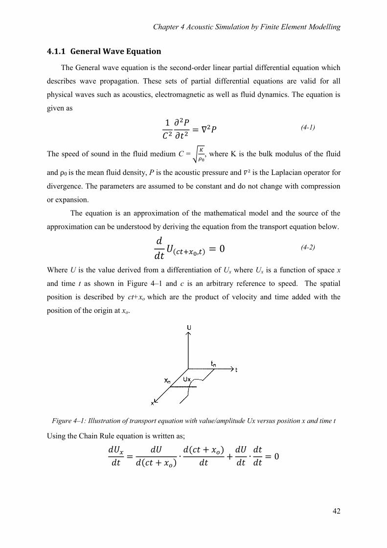
Chapter 4 Acoustic Simulation by Finite Element Modelling
42
4.1.1 General Wave Equation
The General wave equation is the second-order linear partial differential equation which
describes wave propagation. These sets of partial differential equations are valid for all
physical waves such as acoustics, electromagnetic as well as fluid dynamics. The equation is
given as
(4-1)
The speed of sound in the fluid medium C =
, where K is the bulk modulus of the fluid
and ρ0 is the mean fluid density, P is the acoustic pressure and is the Laplacian operator for
divergence. The parameters are assumed to be constant and do not change with compression
or expansion.
The equation is an approximation of the mathematical model and the source of the
approximation can be understood by deriving the equation from the transport equation below.
(4-2)
Where U is the value derived from a differentiation of Ux where Ux is a function of space x
and time t as shown in Figure 4–1 and c is an arbitrary reference to speed. The spatial
position is described by ct+xo which are the product of velocity and time added with the
position of the origin at xo.
Figure 4–1: Illustration of transport equation with value/amplitude Ux versus position x and time t
Using the Chain Rule equation is written as;
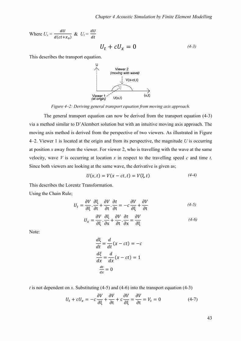
Chapter 4 Acoustic Simulation by Finite Element Modelling
43
Where Ux =
& Ut =
(4-3)
This describes the transport equation.
Figure 4–2: Deriving general transport equation from moving axis approach.
The general transport equation can now be derived from the transport equation (4-3)
via a method similar to D’Alembert solution but with an intuitive moving axis approach. The
moving axis method is derived from the perspective of two viewers. As illustrated in Figure
4–2. Viewer 1 is located at the origin and from its perspective, the magnitude U is occurring
at position x away from the viewer. For viewer 2, who is travelling with the wave at the same
velocity, wave V is occurring at location x in respect to the travelling speed c and time t.
Since both viewers are looking at the same wave, the derivative is given as;
(4-4)
This describes the Lorentz Transformation.
Using the Chain Rule;
(4-5)
(4-6)
Note:
t is not dependent on x. Substituting (4-5) and (4-6) into the transport equation (4-3)
(4-7)
Chapter 4 Acoustic Simulation by Finite Element Modelling
44
To summarize the solution up to this point:
Normal coordinates (viewer 1) U(x,t) Ut + cUx = 0
Moving Coordinates (viewer 2) V(ξ,t) Vt = 0
Since Vt =
= 0, V is independent of time when ξ is viewed strictly as a
coordinate on the x-axis. Therefore Vt = F(ξ). From (4-4), then U(x,t)=F(ξ) = F(x-ct).
Since (4-1) is a directional derivative, the general transport equation of a wave propagating
symmetrically on opposite directions along the x-axis from the origin is written as;
(4-8)
Where F and G are arbitrary functions. The wave equation describes a physical process which
follows the same pattern in space and time. When the amplitude of an oscillator is plotted
against a horizontal position or at a given point against time, both will yield a sine or cosine
wave. This concludes that space and time are symmetrical for oscillators and equation (4-1)
can be proved by substituting a sine function into arbitrary functions F and G of the
space/time transport equation.
Thus,
, and
,
Therefore,
. which proves equation (4-1)
The compliance of equation (4-1) as an acoustic wave equation requires some
assumptions. Firstly the fluid is compressible, but only relatively small pressure changes with
respect to the mean pressure are allowed. The first assumption also reflects that the
displacement is relatively small. Secondly, the fluid is assumed to be non-flowing and
inviscid (where viscosity causes no dissipative effects. Thirdly as mentioned in equation
(4-1), uniform mean density and mean pressure are assumed (hence acoustic speed of
material remains constant). Therefore the pressure solution then becomes a deviation from
the mean pressure, and not the absolute pressure. (Ansys, 2009b)
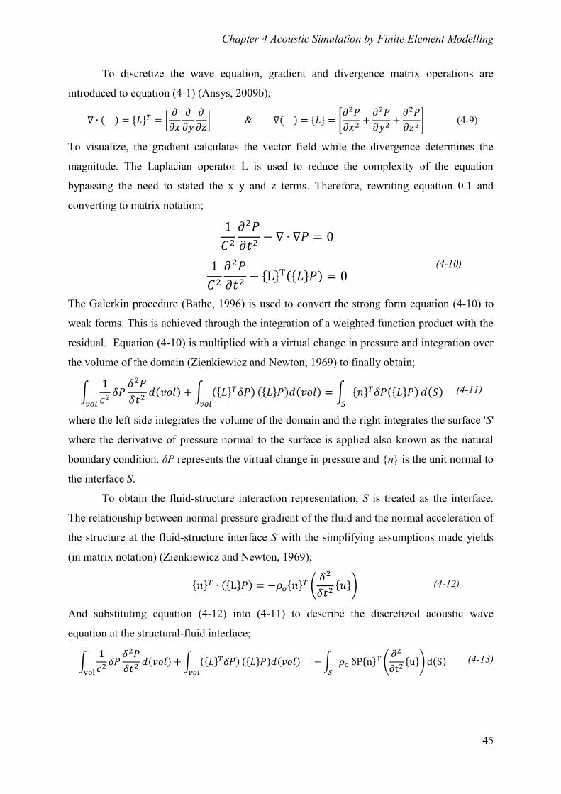
Chapter 4 Acoustic Simulation by Finite Element Modelling
45
To discretize the wave equation, gradient and divergence matrix operations are
introduced to equation (4-1) (Ansys, 2009b);
&
(4-9)
To visualize, the gradient calculates the vector field while the divergence determines the
magnitude. The Laplacian operator L is used to reduce the complexity of the equation
bypassing the need to stated the x y and z terms. Therefore, rewriting equation 0.1 and
converting to matrix notation;
(4-10)
The Galerkin procedure (Bathe, 1996) is used to convert the strong form equation (4-10) to
weak forms. This is achieved through the integration of a weighted function product with the
residual. Equation (4-10) is multiplied with a virtual change in pressure and integration over
the volume of the domain (Zienkiewicz and Newton, 1969) to finally obtain;
(4-11)
where the left side integrates the volume of the domain and the right integrates the surface 'S'
where the derivative of pressure normal to the surface is applied also known as the natural
boundary condition. δP represents the virtual change in pressure and {n} is the unit normal to
the interface S.
To obtain the fluid-structure interaction representation, S is treated as the interface.
The relationship between normal pressure gradient of the fluid and the normal acceleration of
the structure at the fluid-structure interface S with the simplifying assumptions made yields
(in matrix notation) (Zienkiewicz and Newton, 1969);
(4-12)
And substituting equation (4-12) into (4-11) to describe the discretized acoustic wave
equation at the structural-fluid interface;
(4-13)
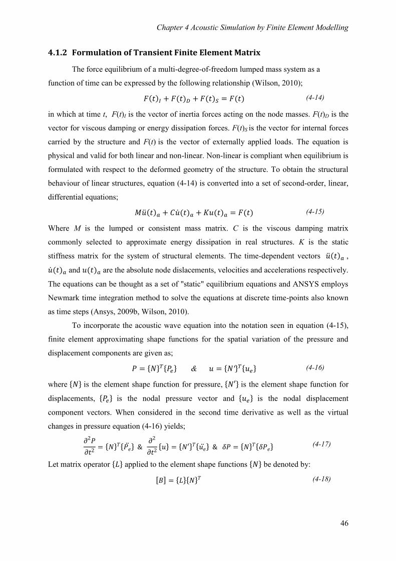
Chapter 4 Acoustic Simulation by Finite Element Modelling
46
4.1.2 Formulation of Transient Finite Element Matrix
The force equilibrium of a multi-degree-of-freedom lumped mass system as a
function of time can be expressed by the following relationship (Wilson, 2010);
(4-14)
in which at time t, F(t)I is the vector of inertia forces acting on the node masses. F(t)D is the
vector for viscous damping or energy dissipation forces. F(t)S is the vector for internal forces
carried by the structure and F(t) is the vector of externally applied loads. The equation is
physical and valid for both linear and non-linear. Non-linear is compliant when equilibrium is
formulated with respect to the deformed geometry of the structure. To obtain the structural
behaviour of linear structures, equation (4-14) is converted into a set of second-order, linear,
differential equations;
(4-15)
Where M is the lumped or consistent mass matrix. C is the viscous damping matrix
commonly selected to approximate energy dissipation in real structures. K is the static
stiffness matrix for the system of structural elements. The time-dependent vectors ,
and are the absolute node dislacements, velocities and accelerations respectively.
The equations can be thought as a set of "static" equilibrium equations and ANSYS employs
Newmark time integration method to solve the equations at discrete time-points also known
as time steps (Ansys, 2009b, Wilson, 2010).
To incorporate the acoustic wave equation into the notation seen in equation (4-15),
finite element approximating shape functions for the spatial variation of the pressure and
displacement components are given as;
& (4-16)
where is the element shape function for pressure, is the element shape function for
displacements, is the nodal pressure vector and is the nodal displacement
component vectors. When considered in the second time derivative as well as the virtual
changes in pressure equation (4-16) yields;
(4-17)
Let matrix operator applied to the element shape functions be denoted by:
(4-18)
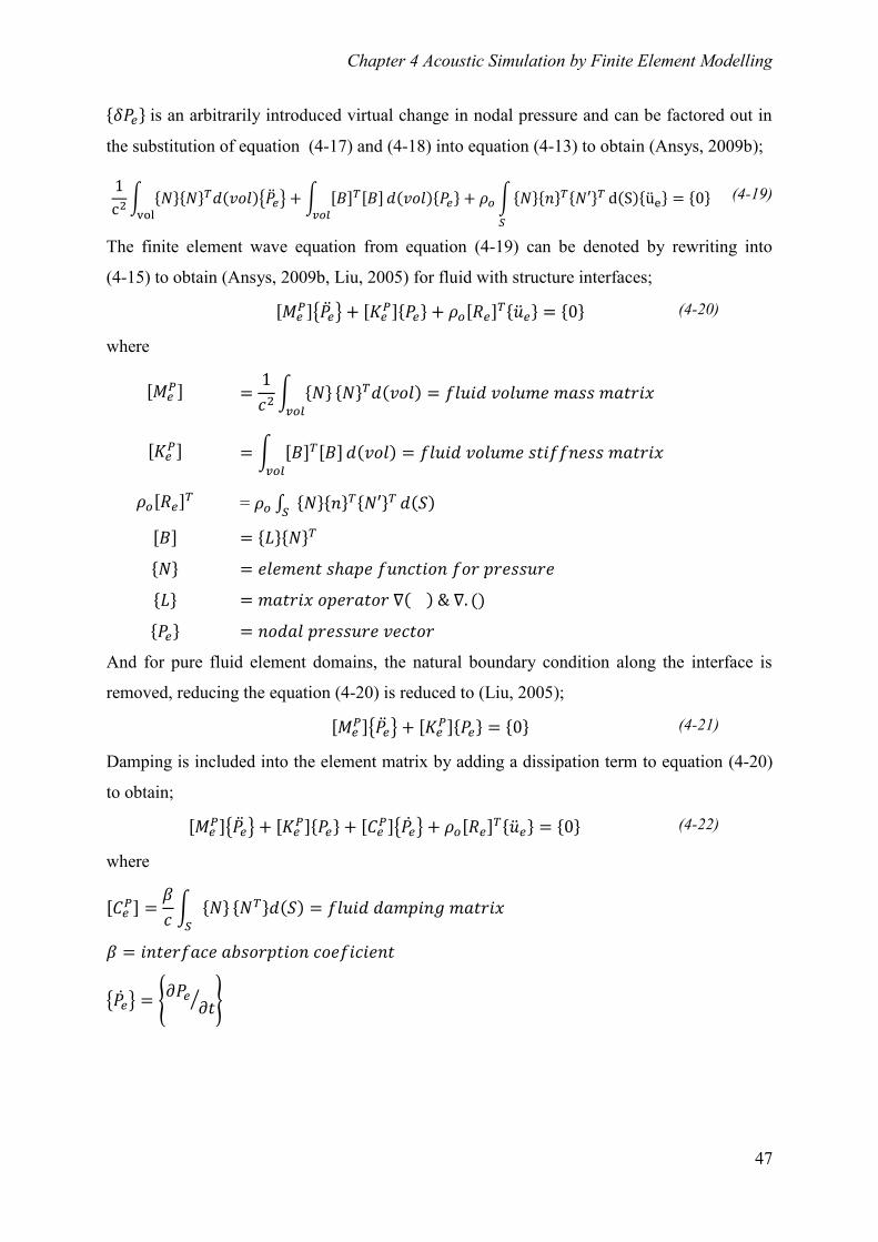
Chapter 4 Acoustic Simulation by Finite Element Modelling
47
is an arbitrarily introduced virtual change in nodal pressure and can be factored out in
the substitution of equation (4-17) and (4-18) into equation (4-13) to obtain (Ansys, 2009b);
(4-19)
The finite element wave equation from equation (4-19) can be denoted by rewriting into
(4-15) to obtain (Ansys, 2009b, Liu, 2005) for fluid with structure interfaces;
(4-20)
where
=
And for pure fluid element domains, the natural boundary condition along the interface is
removed, reducing the equation (4-20) is reduced to (Liu, 2005);
(4-21)
Damping is included into the element matrix by adding a dissipation term to equation (4-20)
to obtain;
(4-22)
where
Chapter 4 Acoustic Simulation by Finite Element Modelling
48
4.2 ANSYS Mechanical Parametric Design Language
Ansys APDL is a multi-physics finite element software package. Also known as Ansys
Mechanical APDL, Ansys mechanical or simply APDL, the finite element software package
differs from Ansys Workbench in its graphics user interface. APDL offers a rudimentary
graphic interface and relies on the console commands and macros codes to carry out
numerical simulations while Ansys Workbench is more geared towards blocked modules and
graphic interface reliance similar to programs such as LabView. Due to the unavailability of
acoustic features in Ansys workbench, this study is carried out entirely from the APDL
console. This offers two benefits; the close understanding of the simulation settings and the
use of macros which facilitates debugging and sharing.
The project is split into three major sections; pre-processing, solution and post-
processing. The pre-processor involved the definition of material properties, declaration of
variables, drawing or import of the model, finite element mesh creation, boundary condition
definitions and setting constraints. The solution phase corresponds to the step where the
functions of each finite element are assembled into a mathematical approximation of the
whole model with the associated initial and input conditions. The solution phase is bespoke to
the type of analysis. For transient work, each solution is represented as a load step which is a
point in time, while for harmonic and modal analysis, the sub steps of a load step corresponds
to the solved natural frequencies and modes. The post-processing features allow visualization
and collection of the resultant data. In most cases, the toolset is unintuitive so exporting the
data to third party programs such as Matlab is more efficient.
The author identifies three areas to pay special attention to when setting up a
simulation project. Firstly, reliable material property values are crucial for an accurate
simulation. Secondly the mesh element also needs to be inspected to have sufficient density
and be defect free. Sometimes, areas or volumes need to be divided manually to achieve the
best result. However, the evaluation of mesh quality is quite subjective albeit obvious. Lastly,
the boundary conditions can sometimes be difficult to define. This is especially true for
elastic constraints or partially damped boundaries. Each of these areas is a discipline in itself.
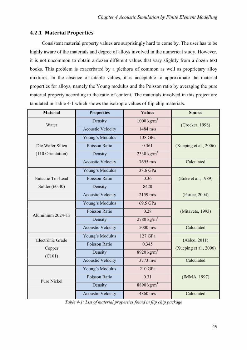
Chapter 4 Acoustic Simulation by Finite Element Modelling
49
4.2.1 Material Properties
Consistent material property values are surprisingly hard to come by. The user has to be
highly aware of the materials and degree of alloys involved in the numerical study. However,
it is not uncommon to obtain a dozen different values that vary slightly from a dozen text
books. This problem is exacerbated by a plethora of common as well as proprietary alloy
mixtures. In the absence of citable values, it is acceptable to approximate the material
properties for alloys, namely the Young modulus and the Poisson ratio by averaging the pure
material property according to the ratio of content. The materials involved in this project are
tabulated in Table 4-1 which shows the isotropic values of flip chip materials.
Material Properties Values Source
Water Density 1000 kg/m
3
(Crocker, 1998) Acoustic Velocity 1484 m/s
Die Wafer Silica
(110 Orientation)
Young’s Modulus 138 GPa
(Xueping et al., 2006) Poisson Ratio 0.361
Density 2330 kg/m3
Acoustic Velocity 7695 m/s Calculated
Eutectic Tin-Lead
Solder (60:40)
Young’s Modulus 38.6 GPa
(Enke et al., 1989) Poisson Ratio 0.36
Density 8420
Acoustic Velocity 2159 m/s (Partee, 2004)
Aluminium 2024-T3
Young’s Modulus 69.5 GPa
(Mitavete, 1993) Poisson Ratio 0.28
Density 2780 kg/m3
Acoustic Velocity 5000 m/s Calculated
Electronic Grade
Copper
(C101)
Young’s Modulus 127 GPa (Aalco, 2011)
(Xueping et al., 2006) Poisson Ratio 0.345
Density 8920 kg/m3
Acoustic Velocity 3773 m/s Calculated
Pure Nickel
Young’s Modulus 210 GPa
(IMMA, 1997) Poisson Ratio 0.31
Density 8890 kg/m3
Acoustic Velocity 4860 m/s Calculated
Table 4-1: List of material properties found in flip chip package
Chapter 4 Acoustic Simulation by Finite Element Modelling
50
Solid region materials are defined using mathematical models which do not require the
acoustic velocities to be input directly. However, the longitudinal wave velocity v is directly
related to the material properties which is given by (Goel, 2007);
(4-23)
Where B is the Bulk modulus, η is the modulus of rigidity and ρ the density of solid material.
In ANSYS for elastic isotropic assumptions, the materials are assumed to be in the form of a
long bar (which constrict the stress strain stiffness to an axis along the bar), the equation can
be reduced into;
(4-24)
Where Y is the Young’s modulus which defines the stress strain ratio along a specific axis.
The option to include young modulus for specific axis as well as other properties like sheer
modulus is available for anisotropic configurations. However for isotropic materials
assumptions, the Y input is used to describe all directions.
4.2.2 Finite Element Types
In Ansys, there are more than a hundred types of elements to choose from. The choices
seem daunting but each element is bespoke to the type of problem. Understanding the
dimensionality (2D or 3D, shell or solid?) and degree of freedom involved (structural, flow,
electromagnetic, pressure, displacements, etc) limits the number of suitable element types,
usually to less than five. The general acoustic structural element is identified as FLUID29 for
two dimensional work with infinite boundary FLUID129 as a companion element to truncate
the computational domain. PLANE42 is used to describe the solid sections of the model. It is
a generic solid element with a specialty for structural degrees of freedom (DOF).
FLUID29 only feature pressure DOFs but can be flagged to include displacement
DOFs for elements in contact with solid surfaces. FLUID29 is applied to any fluid/air areas to
create triangular or quadrilateral element meshes. Triangular meshes are considered to be less
accurate with constant gradients while quadrilateral elements have more nodes that allow
linear gradient functions according to coordinate directions (Pepper and Heinrich, 1992). For
fluid-structure boundaries, one layer of fluid elements in contact with any structure as well as
the nodes which divide the fluid-solid model need to be flagged to invoke fluid-structure
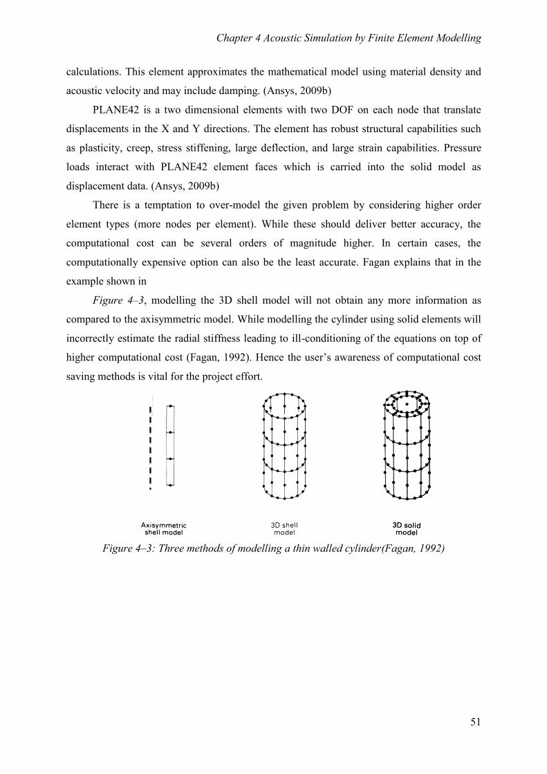
Chapter 4 Acoustic Simulation by Finite Element Modelling
51
calculations. This element approximates the mathematical model using material density and
acoustic velocity and may include damping. (Ansys, 2009b)
PLANE42 is a two dimensional elements with two DOF on each node that translate
displacements in the X and Y directions. The element has robust structural capabilities such
as plasticity, creep, stress stiffening, large deflection, and large strain capabilities. Pressure
loads interact with PLANE42 element faces which is carried into the solid model as
displacement data. (Ansys, 2009b)
There is a temptation to over-model the given problem by considering higher order
element types (more nodes per element). While these should deliver better accuracy, the
computational cost can be several orders of magnitude higher. In certain cases, the
computationally expensive option can also be the least accurate. Fagan explains that in the
example shown in
Figure 4–3, modelling the 3D shell model will not obtain any more information as
compared to the axisymmetric model. While modelling the cylinder using solid elements will
incorrectly estimate the radial stiffness leading to ill-conditioning of the equations on top of
higher computational cost (Fagan, 1992). Hence the user’s awareness of computational cost
saving methods is vital for the project effort.
Figure 4–3: Three methods of modelling a thin walled cylinder(Fagan, 1992)
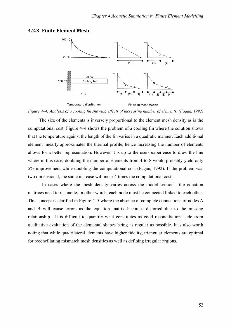
Chapter 4 Acoustic Simulation by Finite Element Modelling
52
4.2.3 Finite Element Mesh
Figure 4–4: Analysis of a cooling fin showing effects of increasing number of elements. (Fagan, 1992)
The size of the elements is inversely proportional to the element mesh density as is the
computational cost. Figure 4–4 shows the problem of a cooling fin where the solution shows
that the temperature against the length of the fin varies in a quadratic manner. Each additional
element linearly approximates the thermal profile, hence increasing the number of elements
allows for a better representation. However it is up to the users experience to draw the line
where in this case, doubling the number of elements from 4 to 8 would probably yield only
5% improvement while doubling the computational cost (Fagan, 1992). If the problem was
two dimensional, the same increase will incur 4 times the computational cost.
In cases where the mesh density varies across the model sections, the equation
matrices need to reconcile. In other words, each node must be connected linked to each other.
This concept is clarified in Figure 4–5 where the absence of complete connections of nodes A
and B will cause errors as the equation matrix becomes distorted due to the missing
relationship. It is difficult to quantify what constitutes as good reconciliation aside from
qualitative evaluation of the elemental shapes being as regular as possible. It is also worth
noting that while quadrilateral elements have higher fidelity, triangular elements are optimal
for reconciliating mismatch mesh densities as well as defining irregular regions.
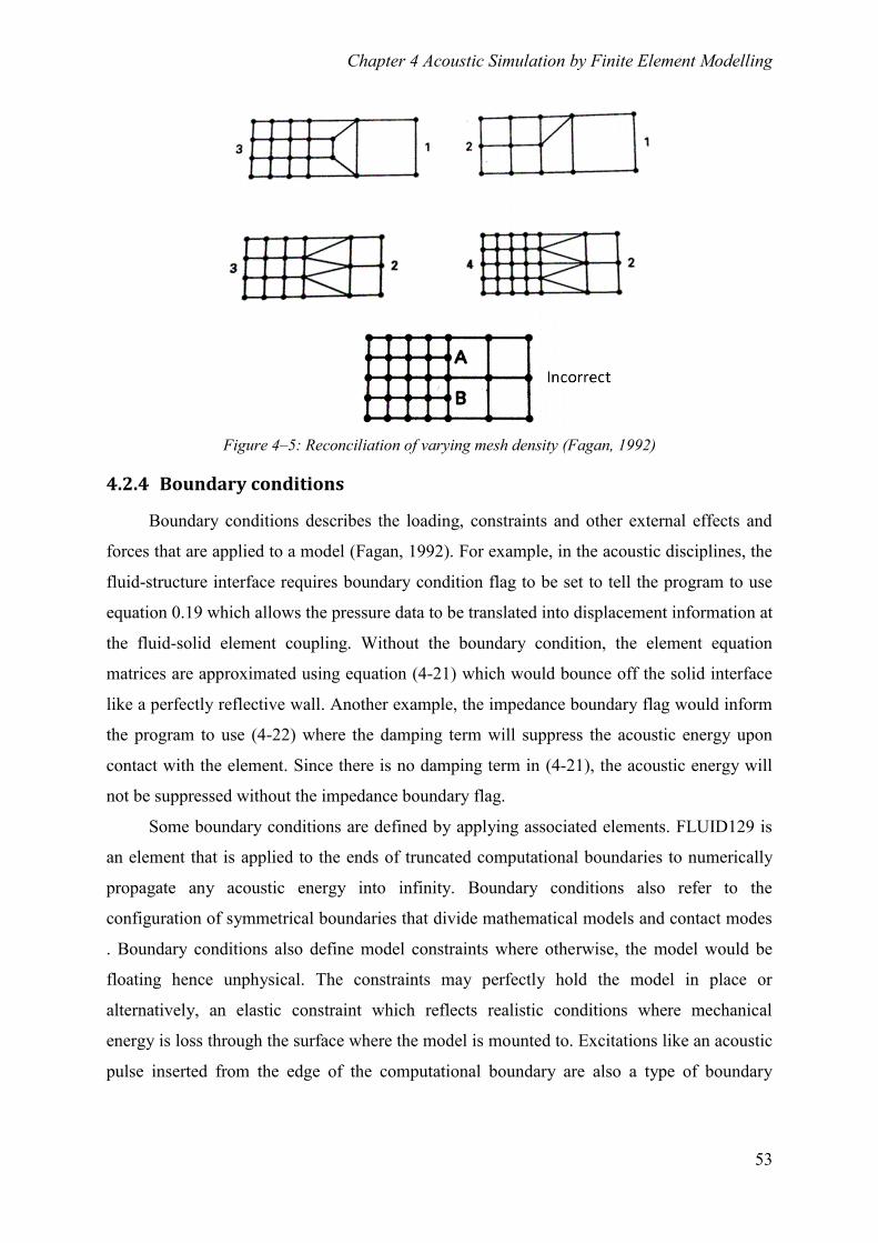
Chapter 4 Acoustic Simulation by Finite Element Modelling
53
Figure 4–5: Reconciliation of varying mesh density (Fagan, 1992)
4.2.4 Boundary conditions
Boundary conditions describes the loading, constraints and other external effects and
forces that are applied to a model (Fagan, 1992). For example, in the acoustic disciplines, the
fluid-structure interface requires boundary condition flag to be set to tell the program to use
equation 0.19 which allows the pressure data to be translated into displacement information at
the fluid-solid element coupling. Without the boundary condition, the element equation
matrices are approximated using equation (4-21) which would bounce off the solid interface
like a perfectly reflective wall. Another example, the impedance boundary flag would inform
the program to use (4-22) where the damping term will suppress the acoustic energy upon
contact with the element. Since there is no damping term in (4-21), the acoustic energy will
not be suppressed without the impedance boundary flag.
Some boundary conditions are defined by applying associated elements. FLUID129 is
an element that is applied to the ends of truncated computational boundaries to numerically
propagate any acoustic energy into infinity. Boundary conditions also refer to the
configuration of symmetrical boundaries that divide mathematical models and contact modes
. Boundary conditions also define model constraints where otherwise, the model would be
floating hence unphysical. The constraints may perfectly hold the model in place or
alternatively, an elastic constraint which reflects realistic conditions where mechanical
energy is loss through the surface where the model is mounted to. Excitations like an acoustic
pulse inserted from the edge of the computational boundary are also a type of boundary
Chapter 4 Acoustic Simulation by Finite Element Modelling
54
condition. While the definition is up for debate, the author argues that the initial conditions
are simply the boundary conditions at the starting time of the transient analysis.
4.3 Acoustic Transient Analysis
There is limited literature on finite element high frequency acoustic transient analysis
(HFATA), and no examples (also known as verification manuals) in Ansys APDL. In the
range of several hundred megahertz and above, this field of study requires enormous
computational resource as shown in (Łodygowski and Sumelka, 2006). This may be the
barrier preventing more publications in this field.
The Ansys help system does state that the acoustic fluid finite elements are capable
for use in transient solutions. This capability is demonstrated in (Liu, 2005). Liu's dissertation
uses both harmonic analysis followed by transient work. An acoustic transient analysis
requires a short acoustic pulse input and many solutions depending on the time step.
Harmonic and modal analysis solves the model natural frequency within a single solution
which requires significantly less time and memory. Unfortunately, Liu's work did not provide
the APDL code to exactly replicate the experiment.
Other similar work using ANSYS are found in the field of laser acoustics. Notable
work by (L'Etang and Huang, 2006, Xu et al., 2006) carries out an uncoupled thermal and
mechanical analysis. The sample is excited with a thermal load where the resultant thermal
response of the nodes is recorded and reapplied in a separate mechanical analysis to obtain
the final stress data.
The numerical experiments using ANSYS found in literature concern frequencies
which are much lower than the 100MHz region required in this study. There is no temporal
limit in governing equations and concerns with numerical stability at higher frequencies are
addressed in subchapter 5.2 below.
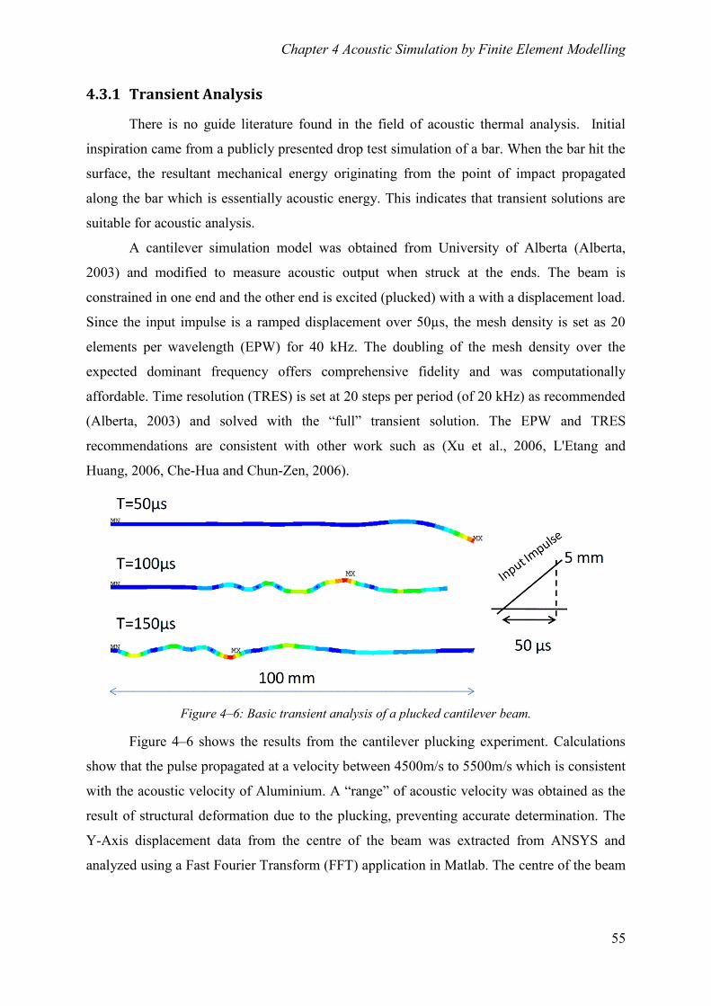
Chapter 4 Acoustic Simulation by Finite Element Modelling
55
4.3.1 Transient Analysis
There is no guide literature found in the field of acoustic thermal analysis. Initial
inspiration came from a publicly presented drop test simulation of a bar. When the bar hit the
surface, the resultant mechanical energy originating from the point of impact propagated
along the bar which is essentially acoustic energy. This indicates that transient solutions are
suitable for acoustic analysis.
A cantilever simulation model was obtained from University of Alberta (Alberta,
2003) and modified to measure acoustic output when struck at the ends. The beam is
constrained in one end and the other end is excited (plucked) with a with a displacement load.
Since the input impulse is a ramped displacement over 50µs, the mesh density is set as 20
elements per wavelength (EPW) for 40 kHz. The doubling of the mesh density over the
expected dominant frequency offers comprehensive fidelity and was computationally
affordable. Time resolution (TRES) is set at 20 steps per period (of 20 kHz) as recommended
(Alberta, 2003) and solved with the “full” transient solution. The EPW and TRES
recommendations are consistent with other work such as (Xu et al., 2006, L'Etang and
Huang, 2006, Che-Hua and Chun-Zen, 2006).
Figure 4–6: Basic transient analysis of a plucked cantilever beam.
Figure 4–6 shows the results from the cantilever plucking experiment. Calculations
show that the pulse propagated at a velocity between 4500m/s to 5500m/s which is consistent
with the acoustic velocity of Aluminium. A “range” of acoustic velocity was obtained as the
result of structural deformation due to the plucking, preventing accurate determination. The
Y-Axis displacement data from the centre of the beam was extracted from ANSYS and
analyzed using a Fast Fourier Transform (FFT) application in Matlab. The centre of the beam
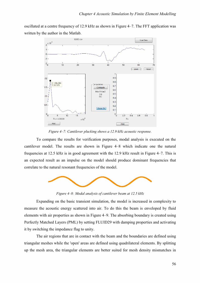
Chapter 4 Acoustic Simulation by Finite Element Modelling
56
oscillated at a centre frequency of 12.9 kHz as shown in Figure 4–7. The FFT application was
written by the author in the Matlab.
Figure 4–7: Cantilever plucking shows a 12.9 kHz acoustic response.
To compare the results for verification purposes, modal analysis is executed on the
cantilever model. The results are shown in Figure 4–8 which indicate one the natural
frequencies at 12.5 kHz is in good agreement with the 12.9 kHz result in Figure 4–7. This is
an expected result as an impulse on the model should produce dominant frequencies that
correlate to the natural resonant frequencies of the model.
Figure 4–8: Modal analysis of cantilever beam at 12.5 kHz
Expanding on the basic transient simulation, the model is increased in complexity to
measure the acoustic energy scattered into air. To do this the beam is enveloped by fluid
elements with air properties as shown in Figure 4–9. The absorbing boundary is created using
Perfectly Matched Layers (PML) by setting FLUID29 with damping properties and activating
it by switching the impedance flag to unity.
The air regions that are in contact with the beam and the boundaries are defined using
triangular meshes while the 'open' areas are defined using quadrilateral elements. By splitting
up the mesh area, the triangular elements are better suited for mesh density mismatches in
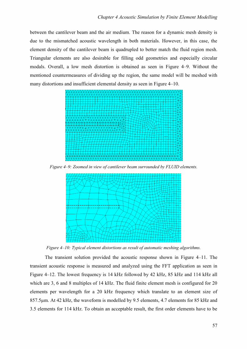
Chapter 4 Acoustic Simulation by Finite Element Modelling
57
between the cantilever beam and the air medium. The reason for a dynamic mesh density is
due to the mismatched acoustic wavelength in both materials. However, in this case, the
element density of the cantilever beam is quadrupled to better match the fluid region mesh.
Triangular elements are also desirable for filling odd geometries and especially circular
modals. Overall, a low mesh distortion is obtained as seen in Figure 4–9. Without the
mentioned countermeasures of dividing up the region, the same model will be meshed with
many distortions and insufficient elemental density as seen in Figure 4–10.
Figure 4–9: Zoomed in view of cantilever beam surrounded by FLUID elements.
Figure 4–10: Typical element distortions as result of automatic meshing algorithms.
The transient solution provided the acoustic response shown in Figure 4–11. The
transient acoustic response is measured and analyzed using the FFT application as seen in
Figure 4–12. The lowest frequency is 14 kHz followed by 42 kHz, 85 kHz and 114 kHz all
which are 3, 6 and 8 multiples of 14 kHz. The fluid finite element mesh is configured for 20
elements per wavelength for a 20 kHz frequency which translate to an element size of
857.5µm. At 42 kHz, the waveform is modelled by 9.5 elements, 4.7 elements for 85 kHz and
3.5 elements for 114 kHz. To obtain an acceptable result, the first order elements have to be
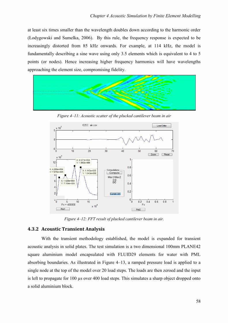
Chapter 4 Acoustic Simulation by Finite Element Modelling
58
at least six times smaller than the wavelength doubles down according to the harmonic order
(Łodygowski and Sumelka, 2006). By this rule, the frequency response is expected to be
increasingly distorted from 85 kHz onwards. For example, at 114 kHz, the model is
fundamentally describing a sine wave using only 3.5 elements which is equivalent to 4 to 5
points (or nodes). Hence increasing higher frequency harmonics will have wavelengths
approaching the element size, compromising fidelity.
Figure 4–11: Acoustic scatter of the plucked cantilever beam in air
Figure 4–12: FFT result of plucked cantilever beam in air.
4.3.2 Acoustic Transient Analysis
With the transient methodology established, the model is expanded for transient
acoustic analysis in solid plates. The test simulation is a two dimensional 100mm PLANE42
square aluminium model encapsulated with FLUID29 elements for water with PML
absorbing boundaries. As illustrated in Figure 4–13, a ramped pressure load is applied to a
single node at the top of the model over 20 load steps. The loads are then zeroed and the input
is left to propagate for 100 µs over 400 load steps. This simulates a sharp object dropped onto
a solid aluminium block.
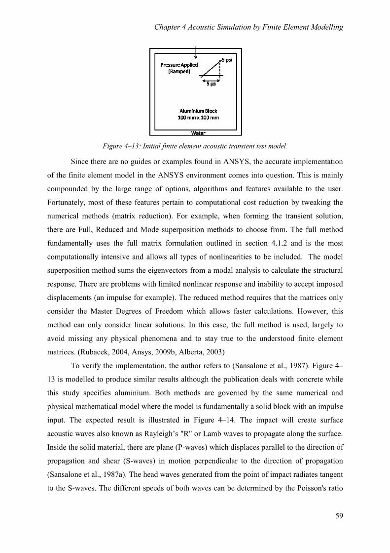
Chapter 4 Acoustic Simulation by Finite Element Modelling
59
Figure 4–13: Initial finite element acoustic transient test model.
Since there are no guides or examples found in ANSYS, the accurate implementation
of the finite element model in the ANSYS environment comes into question. This is mainly
compounded by the large range of options, algorithms and features available to the user.
Fortunately, most of these features pertain to computational cost reduction by tweaking the
numerical methods (matrix reduction). For example, when forming the transient solution,
there are Full, Reduced and Mode superposition methods to choose from. The full method
fundamentally uses the full matrix formulation outlined in section 4.1.2 and is the most
computationally intensive and allows all types of nonlinearities to be included. The model
superposition method sums the eigenvectors from a modal analysis to calculate the structural
response. There are problems with limited nonlinear response and inability to accept imposed
displacements (an impulse for example). The reduced method requires that the matrices only
consider the Master Degrees of Freedom which allows faster calculations. However, this
method can only consider linear solutions. In this case, the full method is used, largely to
avoid missing any physical phenomena and to stay true to the understood finite element
matrices. (Rubacek, 2004, Ansys, 2009b, Alberta, 2003)
To verify the implementation, the author refers to (Sansalone et al., 1987). Figure 4–
13 is modelled to produce similar results although the publication deals with concrete while
this study specifies aluminium. Both methods are governed by the same numerical and
physical mathematical model where the model is fundamentally a solid block with an impulse
input. The expected result is illustrated in Figure 4–14. The impact will create surface
acoustic waves also known as Rayleigh’s "R" or Lamb waves to propagate along the surface.
Inside the solid material, there are plane (P-waves) which displaces parallel to the direction of
propagation and shear (S-waves) in motion perpendicular to the direction of propagation
(Sansalone et al., 1987a). The head waves generated from the point of impact radiates tangent
to the S-waves. The different speeds of both waves can be determined by the Poisson's ratio
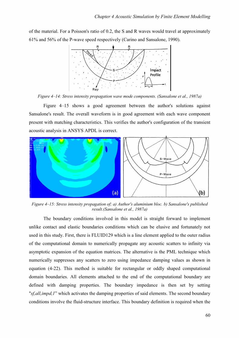
Chapter 4 Acoustic Simulation by Finite Element Modelling
60
of the material. For a Poisson's ratio of 0.2, the S and R waves would travel at approximately
61% and 56% of the P-wave speed respectively (Carino and Sansalone, 1990).
Figure 4–14: Stress intensity propagation wave mode components. (Sansalone et al., 1987a)
Figure 4–15 shows a good agreement between the author's solutions against
Sansalone's result. The overall waveform is in good agreement with each wave component
present with matching characteristics. This verifies the author's configuration of the transient
acoustic analysis in ANSYS APDL is correct.
Figure 4–15: Stress intensity propagation of; a) Author's aluminium bloc. b) Sansalone's published
result.(Sansalone et al., 1987a)
The boundary conditions involved in this model is straight forward to implement
unlike contact and elastic boundaries conditions which can be elusive and fortunately not
used in this study. First, there is FLUID129 which is a line element applied to the outer radius
of the computational domain to numerically propagate any acoustic scatters to infinity via
asymptotic expansion of the equation matrices. The alternative is the PML technique which
numerically suppresses any scatters to zero using impedance damping values as shown in
equation (4-22). This method is suitable for rectangular or oddly shaped computational
domain boundaries. All elements attached to the end of the computational boundary are
defined with damping properties. The boundary impedance is then set by setting
"sf,all,impd,1” which activates the damping properties of said elements. The second boundary
conditions involve the fluid-structure interface. This boundary definition is required when the
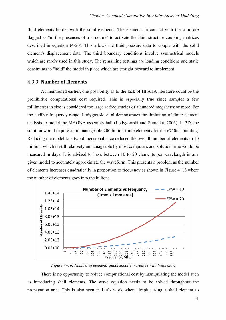
Chapter 4 Acoustic Simulation by Finite Element Modelling
61
fluid elements border with the solid elements. The elements in contact with the solid are
flagged as "in the presences of a structure" to activate the fluid structure coupling matrices
described in equation (4-20). This allows the fluid pressure data to couple with the solid
element's displacement data. The third boundary conditions involve symmetrical models
which are rarely used in this study. The remaining settings are loading conditions and static
constraints to "hold" the model in place which are straight forward to implement.
4.3.3 Number of Elements
As mentioned earlier, one possibility as to the lack of HFATA literature could be the
prohibitive computational cost required. This is especially true since samples a few
millimetres in size is considered too large at frequencies of a hundred megahertz or more. For
the audible frequency range, Łodygowski et al demonstrates the limitation of finite element
analysis to model the MAGNA assembly hall (Łodygowski and Sumelka, 2006). In 3D, the
solution would require an unmanageable 200 billion finite elements for the 6750m3 building.
Reducing the model to a two dimensional slice reduced the overall number of elements to 10
million, which is still relatively unmanageable by most computers and solution time would be
measured in days. It is advised to have between 10 to 20 elements per wavelength in any
given model to accurately approximate the waveform. This presents a problem as the number
of elements increases quadratically in proportion to frequency as shown in Figure 4–16 where
the number of elements goes into the billions.
Figure 4–16: Number of elements quadratically increases with frequency.
There is no opportunity to reduce computational cost by manipulating the model such
as introducing shell elements. The wave equation needs to be solved throughout the
propagation area. This is also seen in Liu’s work where despite using a shell element to
0.0E+00
2.0E+13
4.0E+13
6.0E+13
8.0E+13
1.0E+14
1.2E+14
1.4E+14
5
25
45
65
85
10
5
12
5
14
5
16
5
18
5
20
5
22
5
24
5
26
5
28
5
30
5
32
5
34
5
36
5
38
5
Nu
mb
er
of
Ele
me
nts
Frequency, MHz
Number of Elements vs Frequency (1mm x 1mm area)
EPW = 10
EPW = 20
Chapter 4 Acoustic Simulation by Finite Element Modelling
62
model a human skull, the region encapsulated by the shell still required fluid elements
(Figure 4–17). A harmonic analysis of a submerged ring by (Schroeder et al., 1976) and
radiating sphere by (Imaoka, 2013) also demonstrates the painful amount of elements
required successfully carry out a simple simulation. Schroeder’s publication is also used as a
verification simulation in Ansys; hence the source code (VM177) is publicly available.
Imaoka is a subject leader and the cited code is introduced to new users as the basic method
to carry out harmonic and modal analysis.
Figure 4–17: Simplified model of human skull for acoustic transient analysis.(Liu, 2005)
4.3.4 Reducing Number of Elements
Figure 4–18: Demonstration of dynamic mesh density
Boundary conditions and transient analysis methodologies aside, the last remaining
challenge in HFATA is the management of computational expense. Two methods are applied.
The first involve varying dynamic mesh density. The propagation paths itself require
sufficient element density to maintain the fidelity of the waveform. However, the path can be
isolated where the path itself has high element density and the surrounding area, especially
the buffer regions can be constructed with lower elements per wavelengths (EPW). This will
Figure Permission not obtained.
Please Refer Citation
Figure 3.8 Page 29
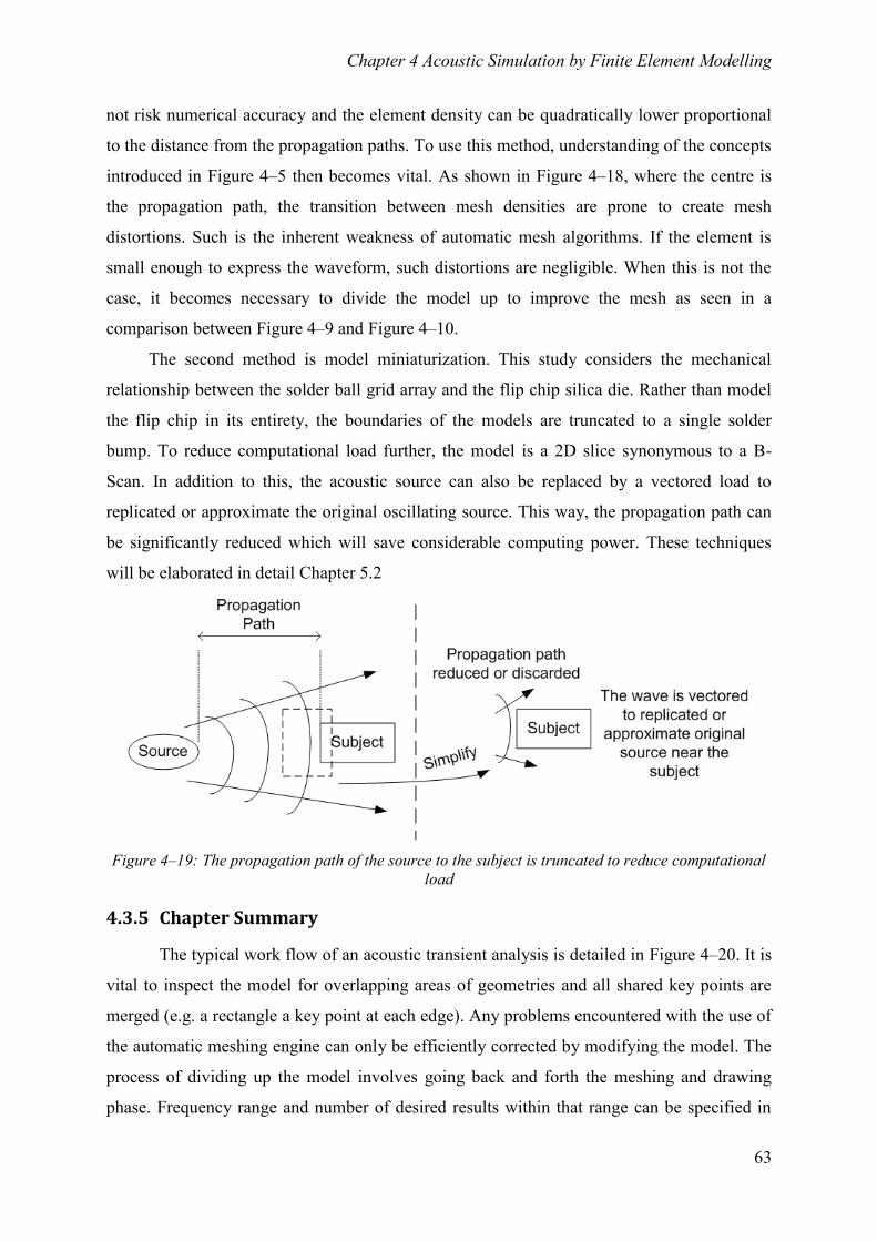
Chapter 4 Acoustic Simulation by Finite Element Modelling
63
not risk numerical accuracy and the element density can be quadratically lower proportional
to the distance from the propagation paths. To use this method, understanding of the concepts
introduced in Figure 4–5 then becomes vital. As shown in Figure 4–18, where the centre is
the propagation path, the transition between mesh densities are prone to create mesh
distortions. Such is the inherent weakness of automatic mesh algorithms. If the element is
small enough to express the waveform, such distortions are negligible. When this is not the
case, it becomes necessary to divide the model up to improve the mesh as seen in a
comparison between Figure 4–9 and Figure 4–10.
The second method is model miniaturization. This study considers the mechanical
relationship between the solder ball grid array and the flip chip silica die. Rather than model
the flip chip in its entirety, the boundaries of the models are truncated to a single solder
bump. To reduce computational load further, the model is a 2D slice synonymous to a B-
Scan. In addition to this, the acoustic source can also be replaced by a vectored load to
replicated or approximate the original oscillating source. This way, the propagation path can
be significantly reduced which will save considerable computing power. These techniques
will be elaborated in detail Chapter 5.2
Figure 4–19: The propagation path of the source to the subject is truncated to reduce computational
load
4.3.5 Chapter Summary
The typical work flow of an acoustic transient analysis is detailed in Figure 4–20. It is
vital to inspect the model for overlapping areas of geometries and all shared key points are
merged (e.g. a rectangle a key point at each edge). Any problems encountered with the use of
the automatic meshing engine can only be efficiently corrected by modifying the model. The
process of dividing up the model involves going back and forth the meshing and drawing
phase. Frequency range and number of desired results within that range can be specified in
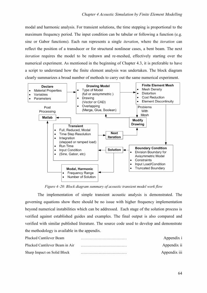
Chapter 4 Acoustic Simulation by Finite Element Modelling
64
modal and harmonic analysis. For transient solutions, the time stepping is proportional to the
maximum frequency period. The input condition can be tabular or following a function (e.g.
sine or Gabor functions). Each run represents a single iteration, where the iteration can
reflect the position of a transducer or for structural nonlinear cases, a bent beam. The next
iteration requires the model to be redrawn and re-meshed, effectively starting over the
numerical experiment. As mentioned in the beginning of Chapter 4.3, it is preferable to have
a script to understand how the finite element analysis was undertaken. The block diagram
clearly summarizes a broad number of methods to carry out the same numerical experiment.
Figure 4–20: Block diagram summary of acoustic transient model work flow
The implementation of simple transient acoustic analysis is demonstrated. The
governing equations show there should be no issue with higher frequency implementation
beyond numerical instabilities which can be addressed. Each stage of the solution process is
verified against established guides and examples. The final output is also compared and
verified with similar published literature. The source code used to develop and demonstrate
the methodology is available in the appendix.
Plucked Cantilever Beam ……………………………… Appendix i
Plucked Cantilever Beam in Air ……………………………… Appendix ii
Sharp Impact on Solid Block ……………………………… Appendix iii
Chapter 5 Finite Element Development
65
Chapter 5
Finite Element Development
Chapter 5 Finite Element Development
66
5 Finite Element Development
In this chapter, two aspects of the finite element methods are explored. Firstly, the
following section explores the feasibility of implementation quadrilateral infinite absorbing
boundaries using traditional circular elements. This is achieved by defining a very large
radius for the circular infinite boundary which is a novel approach.
The second part of this chapter explores the optimal time and spatial resolution
configuration achievable within the computational budget. While this particular point has
been discussed heavily, it is worth testing the accepted norms with empirical data. It is also
prudent to examine the solution convergence specific to the implementations of this study.
5.1 Development of Quadrilateral Infinite Absorbing Boundary
Technique
As outlined in chapter 4.3.4, one of the challenges of finite element modelling
especially for acoustic solutions is the management of element density. The primary
management methodology is to reduce the overall size of the computational model. This field
of study is deep and is its own discipline which is known as truncated boundaries. The ideal
truncated boundary does only one thing, which is to limit the computational boundary while
introducing zero scatter or artefact signals. This is achieved by realizing the Dirichlet-to-
Neumann radiation condition or DtN map in short (Oberai et al., 1998). Traditionally, DtN
methodologies suffer from implementation barriers as well as high computational demands
(Kallivokas and Lee, 2004).
Absorbing boundary conditions (ABC) are usually developed as circular or elliptical
boundary geometries and can be loosely categorized as non-local and local techniques with
exception to Perfectly Matched Layer (PML) (Kallivokas and Lee, 2004).Generally, non-
local techniques are developed to satisfy the DtN criteria hence is exact and non-reflecting or
ideal while local ABC like infinite elements realizes an approximate solution via asymptotic
expansion of the far field solution which sacrifices accuracy in favour of much lower
computing demand. The PML method realizes the boundary condition by numerically forcing
a damping coefficient to eliminate scatter. This method splits the boundary elements into
lossless and dissipative elements that damp the wave that interfaces with it. This translates to
the need to mesh an additional layer of dissipative elements to envelope the computational
domain. Unlike local methods which are coupled to the boundary line of circular or elliptical
Chapter 5 Finite Element Development
67
boundaries, PML can be meshed around the computational domain in any complex absorbing
boundary geometries.
The geometrical weakness of circular boundaries has encouraged a variety of
developments of elliptical boundaries like (Kallivokas and Lee, 2004) and (Medvinsky et al.,
2008). While an elliptical boundary does reduce the computational domain significantly,
unlike a circle, it is relatively troublesome to implement when coupling with the vector
drawing. For this work, microelectronic package simulations usually involve rectangular flip
chip cross-sections. The geometry for most electronic packages is horizontally long and
vertically short, and to simulate acoustic microscopy work, the area of interest traverses the
model horizontally to emulate industrial ultrasound inspection (Chean Lee, 2012). It is
advantageous to use a rectangular boundary to optimally truncate the computational domain.
However, most local techniques including the infinite boundary are designed to be circular
with a requirement to specify the spatial parameters of the circle. Although the PML method
has the advantage of free geometric configuration, the performance of an infinite boundary is
better under specific conditions (Gomez-Revuelto et al., 2012). Since PML is an unphysical
methodology (Basu and Chopra, 2003), there arises accuracy concerns.
For ANSYS, the infinite boundary technique is called FLUID129 which is a
companion element to the popular FLUID29 acoustic fluid element. This element is realized
as a line element and is meshed on a circular truncated boundary with compulsory matching
spatial specifications for the circular geometry. To use the PML method, the absorbing
boundary is created by specifying impedance or damping value (typically 1 for 100%
damping) on a FLUID29 element and applying that layer of elements enveloping the
computational boundary. It is important to remember that FLUID129 infinite boundaries are
always circular while PML FLUID29 technique has geometric freedom.
The objective of this section is to explore a methodology of merging the performance
of an infinite boundary with the configuration freedom of the PML method. The idea was to
apply and test the viability of applying FLUID129 circular absorbing boundary on a square
truncated domain. To achieve this, the radius of the infinite boundary equation is assigned a
very large value. The large value translates into a curvature approaching zero to realize a
straight line boundary. The straight infinite boundary is meshed unto the computational
domain like using regular circular FLUID129 methods. This also means that the boundary is
discontinuous, and the corners of the absorbing boundaries are realized by adding multiple
infinite boundary definitions. The exploitation of the radius size to map straight boundaries
has not been found in any publication thus far. The second condition is that the boundary is
Chapter 5 Finite Element Development
68
realized very close to the scatter source to aggressively reduce the computational domain. All
simulations are carried out with the boundary at a distance of one lambda (of the dominant
frequency) from the solid interface. This technique is dubbed the "Quadrilateral Infinite
Boundary" (QIB).
5.1.1 ANSYS element FLUID129 and PML absorbing techniques
The primary difficulty of modelling infinite medium comes from the need to satisfy
the Sommerfeld radiation condition (Ansys, 2009b);
(5-1)
Where r is the distance of the infinite medium from the origin, Pr is the pressure derivative
along the radial direction, and d is the dimensionality of the problem. The Fluid129 element
tackles this problem by truncating the unbounded domain with an absorbing artificial
boundary. This is realized by (Kallivokas et al.) in two dimensions as;
(5-2)
Where n is the outward normal to curve, Pn is pressure derivative in the normal direction, Pλλ
is the pressure derivative along curve, k is the curvature, and γ is a stability parameter. Since
the curvature or radius 'k' of Kallivokas's infinite boundary solution is arbitrary to Pn and Pλλ,
a very large radius definition will not increase computational complexity. While FLUID129
applies an infinite boundary as a line on the boundary of the computational domain,
FLUID29 acoustic fluid element has the ability to employ the PML technique. This method
works by splitting the element into lossless and dissipative regions where the dissipative
regions is the absorbing boundary usually one element in thickness. The equation is realized
by including additional dissipative effects to the lossless wave equation. The PML equation
for dissipative element is give as (Craggs, 1986):
(5-3)
Where P is the acoustic pressure, δP is the virtual change in pressure, [L] is the divergence
matrix, [L]T is the gradient matrix, c is the speed of sound in acoustic medium, ρ0 is the mean
fluid density, and r is the absorption coefficient at the boundary.
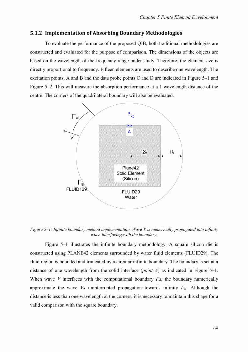
Chapter 5 Finite Element Development
69
5.1.2 Implementation of Absorbing Boundary Methodologies
To evaluate the performance of the proposed QIB, both traditional methodologies are
constructed and evaluated for the purpose of comparison. The dimensions of the objects are
based on the wavelength of the frequency range under study. Therefore, the element size is
directly proportional to frequency. Fifteen elements are used to describe one wavelength. The
excitation points, A and B and the data probe points C and D are indicated in Figure 5–1 and
Figure 5–2. This will measure the absorption performance at a 1 wavelength distance of the
centre. The corners of the quadrilateral boundary will also be evaluated.
Plane42
Solid Element
(Silicon)
FLUID29
Water
FLUID129
A
xxxx
1λ2λ
xCΓ∞
Γa
V
Figure 5–1: Infinite boundary method implementation. Wave V is numerically propagated into infinity
when interfacing with the boundary.
Figure 5–1 illustrates the infinite boundary methodology. A square silicon die is
constructed using PLANE42 elements surrounded by water fluid elements (FLUID29). The
fluid region is bounded and truncated by a circular infinite boundary. The boundary is set at a
distance of one wavelength from the solid interface (point A) as indicated in Figure 5–1.
When wave V interfaces with the computational boundary Γa, the boundary numerically
approximate the wave Vs uninterrupted propagation towards infinity Γ∞. Although the
distance is less than one wavelength at the corners, it is necessary to maintain this shape for a
valid comparison with the square boundary.
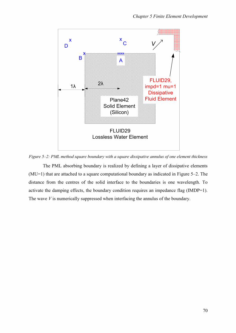
Chapter 5 Finite Element Development
70
Plane42
Solid Element
(Silicon)
FLUID29
Lossless Water Element
FLUID29,
impd=1 mu=1
Dissipative
Fluid Element
A
xxxxxB
xC
x
D V
1λ2λ
Figure 5–2: PML method square boundary with a square dissipative annulus of one element thickness
The PML absorbing boundary is realized by defining a layer of dissipative elements
(MU=1) that are attached to a square computational boundary as indicated in Figure 5–2. The
distance from the centres of the solid interface to the boundaries is one wavelength. To
activate the damping effects, the boundary condition requires an impedance flag (IMDP=1).
The wave V is numerically suppressed when interfacing the annulus of the boundary.
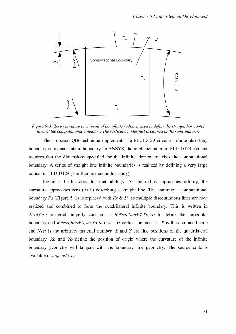
Chapter 5 Finite Element Development
71
r→∞
Γ∞
FL
UID
12
9
Γy
Γx
Computational Boundary
V
θ≈0˚
r→∞
Figure 5–3: Zero curvature as a result of an infinite radius is used to define the straight horizontal
lines of the computational boundary. The vertical counterpart is defined in the same manner.
The proposed QIB technique implements the FLUID129 circular infinite absorbing
boundary on a quadrilateral boundary. In ANSYS, the implementation of FLUID129 element
requires that the dimensions specified for the infinite element matches the computational
boundary. A series of straight line infinite boundaries is realized by defining a very large
radius for FLUID129 (1 million meters in this study).
Figure 5–3 illustrates this methodology. As the radius approaches infinity, the
curvature approaches zero (θ≈0˚) describing a straight line. The continuous computational
boundary Γa (Figure 5–1) is replaced with Γx & Γy as multiple discontinuous lines are now
realized and combined to form the quadrilateral infinite boundary. This is written in
ANSYS’s material property constant as R,Nset,Rad+Y,Xo,Yo to define the horizontal
boundary and R,Nset,Rad+X,Xo,Yo to describe vertical boundaries. R is the command code
and Nset is the arbitrary material number. X and Y are line positions of the quadrilateral
boundary. Xo and Yo define the position of origin where the curvature of the infinite
boundary geometry will tangent with the boundary line geometry. The source code is
available in Appendix iv.
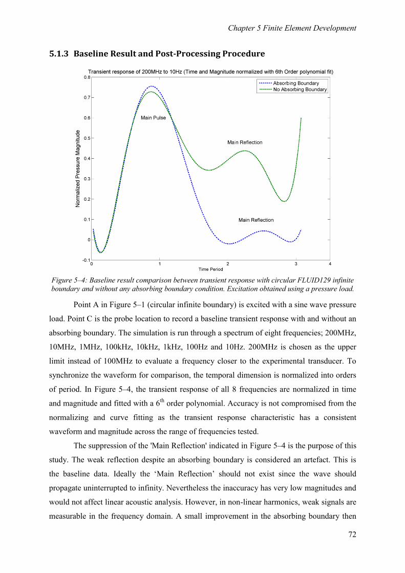
Chapter 5 Finite Element Development
72
5.1.3 Baseline Result and Post-Processing Procedure
Figure 5–4: Baseline result comparison between transient response with circular FLUID129 infinite
boundary and without any absorbing boundary condition. Excitation obtained using a pressure load.
Point A in Figure 5–1 (circular infinite boundary) is excited with a sine wave pressure
load. Point C is the probe location to record a baseline transient response with and without an
absorbing boundary. The simulation is run through a spectrum of eight frequencies; 200MHz,
10MHz, 1MHz, 100kHz, 10kHz, 1kHz, 100Hz and 10Hz. 200MHz is chosen as the upper
limit instead of 100MHz to evaluate a frequency closer to the experimental transducer. To
synchronize the waveform for comparison, the temporal dimension is normalized into orders
of period. In Figure 5–4, the transient response of all 8 frequencies are normalized in time
and magnitude and fitted with a 6th
order polynomial. Accuracy is not compromised from the
normalizing and curve fitting as the transient response characteristic has a consistent
waveform and magnitude across the range of frequencies tested.
The suppression of the 'Main Reflection' indicated in Figure 5–4 is the purpose of this
study. The weak reflection despite an absorbing boundary is considered an artefact. This is
the baseline data. Ideally the ‘Main Reflection’ should not exist since the wave should
propagate uninterrupted to infinity. Nevertheless the inaccuracy has very low magnitudes and
would not affect linear acoustic analysis. However, in non-linear harmonics, weak signals are
measurable in the frequency domain. A small improvement in the absorbing boundary then
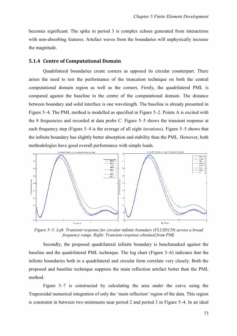
Chapter 5 Finite Element Development
73
becomes significant. The spike in period 3 is complex echoes generated from interactions
with non-absorbing features. Artefact waves from the boundaries will unphysically increase
the magnitude.
5.1.4 Centre of Computational Domain
Quadrilateral boundaries create corners as opposed its circular counterpart. There
arises the need to test the performance of the truncation technique on both the central
computational domain region as well as the corners. Firstly, the quadrilateral PML is
compared against the baseline in the centre of the computational domain. The distance
between boundary and solid interface is one wavelength. The baseline is already presented in
Figure 5–4. The PML method is modelled as specified in Figure 5–2. Points A is excited with
the 8 frequencies and recorded at data probe C. Figure 5–5 shows the transient response at
each frequency step (Figure 5–4 is the average of all eight iterations). Figure 5–5 shows that
the infinite boundary has slightly better absorption and stability than the PML. However, both
methodologies have good overall performance with simple loads.
Figure 5–5: Left: Transient response for circular infinite boundary (FLUID129) across a broad
frequency range. Right: Transient response obtained from PML
Secondly, the proposed quadrilateral infinite boundary is benchmarked against the
baseline and the quadrilateral PML technique. The log chart (Figure 5–6) indicates that the
infinite boundaries both in a quadrilateral and circular form correlate very closely. Both the
proposed and baseline technique suppress the main reflection artefact better than the PML
method.
Figure 5–7 is constructed by calculating the area under the curve using the
Trapezoidal numerical integration of only the ‘main reflection’ region of the data. This region
is constraint in between two minimums near period 2 and period 3 in Figure 5–4. In an ideal
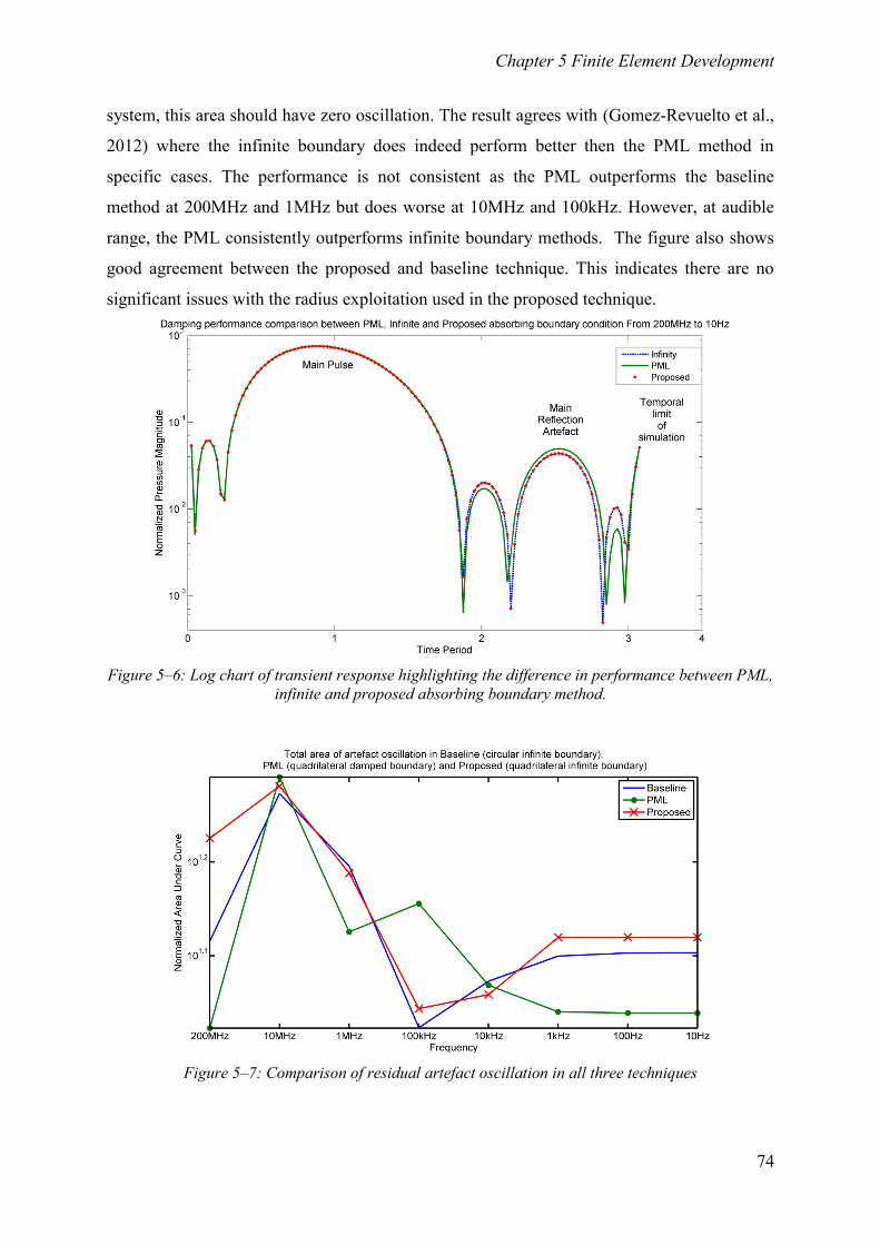
Chapter 5 Finite Element Development
74
system, this area should have zero oscillation. The result agrees with (Gomez-Revuelto et al.,
2012) where the infinite boundary does indeed perform better then the PML method in
specific cases. The performance is not consistent as the PML outperforms the baseline
method at 200MHz and 1MHz but does worse at 10MHz and 100kHz. However, at audible
range, the PML consistently outperforms infinite boundary methods. The figure also shows
good agreement between the proposed and baseline technique. This indicates there are no
significant issues with the radius exploitation used in the proposed technique.
Figure 5–6: Log chart of transient response highlighting the difference in performance between PML,
infinite and proposed absorbing boundary method.
Figure 5–7: Comparison of residual artefact oscillation in all three techniques
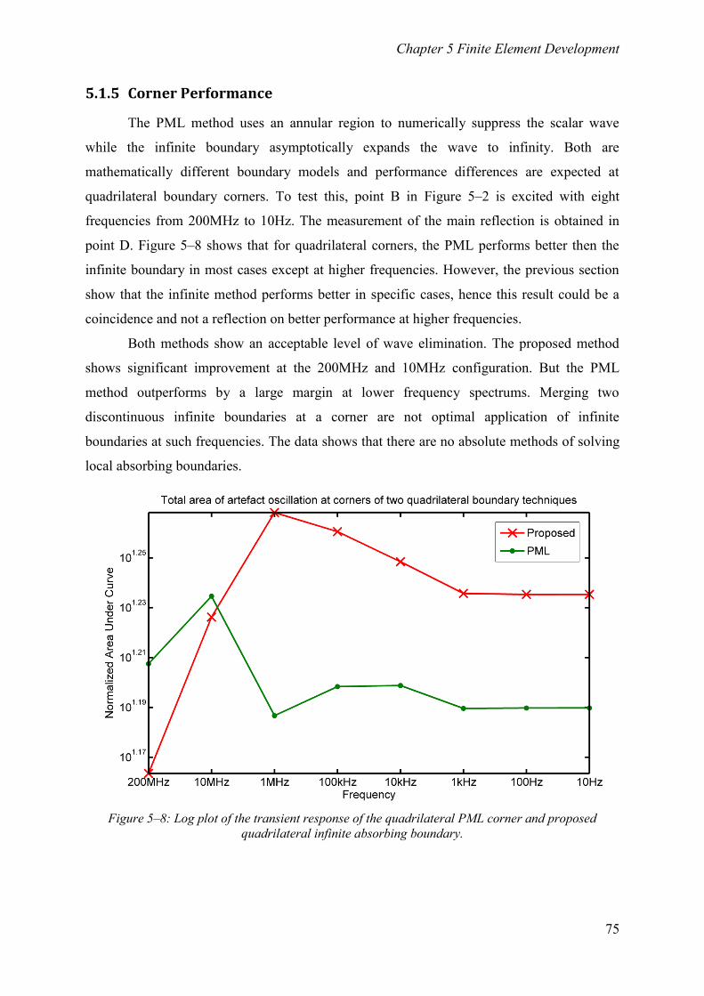
Chapter 5 Finite Element Development
75
5.1.5 Corner Performance
The PML method uses an annular region to numerically suppress the scalar wave
while the infinite boundary asymptotically expands the wave to infinity. Both are
mathematically different boundary models and performance differences are expected at
quadrilateral boundary corners. To test this, point B in Figure 5–2 is excited with eight
frequencies from 200MHz to 10Hz. The measurement of the main reflection is obtained in
point D. Figure 5–8 shows that for quadrilateral corners, the PML performs better then the
infinite boundary in most cases except at higher frequencies. However, the previous section
show that the infinite method performs better in specific cases, hence this result could be a
coincidence and not a reflection on better performance at higher frequencies.
Both methods show an acceptable level of wave elimination. The proposed method
shows significant improvement at the 200MHz and 10MHz configuration. But the PML
method outperforms by a large margin at lower frequency spectrums. Merging two
discontinuous infinite boundaries at a corner are not optimal application of infinite
boundaries at such frequencies. The data shows that there are no absolute methods of solving
local absorbing boundaries.
Figure 5–8: Log plot of the transient response of the quadrilateral PML corner and proposed
quadrilateral infinite absorbing boundary.
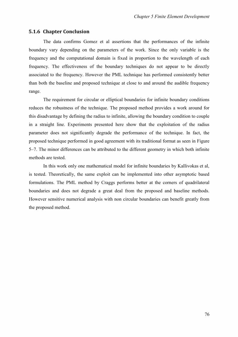
Chapter 5 Finite Element Development
76
5.1.6 Chapter Conclusion
The data confirms Gomez et al assertions that the performances of the infinite
boundary vary depending on the parameters of the work. Since the only variable is the
frequency and the computational domain is fixed in proportion to the wavelength of each
frequency. The effectiveness of the boundary techniques do not appear to be directly
associated to the frequency. However the PML technique has performed consistently better
than both the baseline and proposed technique at close to and around the audible frequency
range.
The requirement for circular or elliptical boundaries for infinite boundary conditions
reduces the robustness of the technique. The proposed method provides a work around for
this disadvantage by defining the radius to infinite, allowing the boundary condition to couple
in a straight line. Experiments presented here show that the exploitation of the radius
parameter does not significantly degrade the performance of the technique. In fact, the
proposed technique performed in good agreement with its traditional format as seen in Figure
5–7. The minor differences can be attributed to the different geometry in which both infinite
methods are tested.
In this work only one mathematical model for infinite boundaries by Kallivokas et al,
is tested. Theoretically, the same exploit can be implemented into other asymptotic based
formulations. The PML method by Craggs performs better at the corners of quadrilateral
boundaries and does not degrade a great deal from the proposed and baseline methods.
However sensitive numerical analysis with non circular boundaries can benefit greatly from
the proposed method.
Chapter 5 Finite Element Development
77
5.2 Evaluation of Numerical Dispersion Error for Acoustic Transient
Analysis
Numerical Dispersion Error is a well known and well publicized issue in numerical
studies. This largely affects harmonic wave analysis and especially transient wave
propagation studies with increasing wave numbers (Ham and Bathe, 2012). Finite element
methods have assumptions and simplification that reduces the ability of the polynomial basis
function to form an exact representation of the field (Bin, 2004, Warren and Scott, 1998).
Finite precision in the element will significantly degrade in accuracy especially in time
stepped solutions typical of transient studies (Scott, 1994). Period elongation and amplitude
decay (Ham and Bathe, 2012) can cause wave propagation velocity to be significantly
different from the physical velocity resulting in dispersion and dissipation errors (Idesman et
al., 2011).
The spatial (element per wavelength) and temporal (time step) resolution of the
simulation can be set as an arbitrary number or by satisfying an equation. L’Etang et al
suggest a both temporal and spatial resolution of 20 points per period and 20 elements per
smallest wavelength respectively should be used (L'Etang and Huang, 2006). 20 elements per
minimum wavelength will solve numerical problems to a 0.1% error (Mohamed and Masson,
2011). However, Che-Hua et al relaxes the spatial parameters by enforcing the mesh size
hspace to meet the criteria of (Che-Hua and Chun-Zen, 2006);
(5-4)
Where λmin is the minimum wavelength in the numerical model. Hence lowering the required
h value from 20 to 15. To maintain numerical stability, the temporal resolution, htime is given
as (Sansalone et al., 1987b);
(5-5)
Where L represents the shortest dimension of the finite element mapped in the model. Both
equation (5-4) and (5-5) can be linked by replacing L with hspace. C specifies the material
acoustic velocity of the model. The equation (5-5) specifies a time step relationship
proportional to the size of the finite element which differs with L’Etang et al’s method where
the h values are directly specified.
In Sansalone’s work, the element size was configured as 0.02 times the plate
thickness of 0.25m and 0.5m, with a fixed material velocity of 4000m/s. These values are
substituted into equation (5-5) to yield an htime of 1.25µs and 2.5µs respectively. The paper
Chapter 5 Finite Element Development
78
uses an excitation impulse of 25µs to 31µs which has a frequency range between 16kHz to
20kHz. For brevity, consider the smallest time step htime for a 20kHz centre frequency. If the
desired sampling resolution is 20 load steps per period, htime will be 2.5µs and 1.67µs
respectively for 30 load steps per period. Manual pixel measurements of the figures show a
frequency response of 7kHz and 116MHz. In both cases, the calculated time step, htime is
either too high or too low. Hence it may be preferable to directly specify h values based on
the specific work.
The evaluation of numerical error is confined to two parameters which are time step
resolution and element density resolution. These two parameters are the main factors in
determining the simulation fidelity and computation time needed for the solution. Large
numbers of time steps have a linear increase in computational load while element density
have a quadratic load increase since it is defined by the number of elements in a given area or
volume.
Quadrilateral elements can reduce numerical destabilization (Fierz et al., 2012). When
meshed these elements align neatly for simple geometries which lead to cleaner results on top
of being able to specify linear gradients in all directions (Pepper and Heinrich, 1992).
Triangular elements have greater flexibility in mapping odd geometric shapes and filling
corners. However, the gradient calculation is not as accurate as quadrilateral elements as
stated by Pepper et al. Since this work is interested in error generation, the model is
constructed using triangular elements to exacerbate any errors. In addition, the main project
uses triangular elements to describe the water medium which couples the transducer to the
sample. The parameters are setup into 33 combinations and evaluated using ANSYS APDL.
Chapter 5 Finite Element Development
79
5.2.1 Motivation and Objective
The primary method of reducing numerical dispersion error is by increasing spatial
and temporal resolution of the numerical model. However without empirical evidence, it is
difficult to justify which configurations are optimal. Ideally with enough computing power,
the numerical experiment can be setup with a hundred elements per wavelength (EPW) and a
hundred time steps per period (T_RES) or more. Unfortunately, a compromise has to be met
in regards to available computing power.
Various published and informal literature have widely noted that 20 element per
wavelength (EPW) is considered the high end of nodal density. This defines the number of
dots, and subsequent lines connecting them to form elements, used to describe a geometry.
However, both element density and time step resolution affects the sampling quality. Using
20 elements to describe a wave literally assigns 21 nodes to form the wave. Each time step
extrapolates the wave’s position in time and space. A time step that is too large will result in
missing behaviour. The error will worsen as the following time step increments are then
extrapolated from the previous time step of erroneous results. Hence the definition of
'sampling frequency' is slightly different. Usually, sampling frequency is the rate of periodic
data acquisition. However, the sampling frequency in numerical models cannot exceed the
limits of the time step. However, in the case of (Sansalone et al., 1987b), the data was
sampled at 2µs intervals although the time step was at 1µs intervals. Therefore the sampling
rate was only half of what was obtainable from the model. This practice does not appear to be
advantageous.
The necessity of this work stems from numerical problems being naturally explicit.
By conduction a solution correlation study, this work aims to analyze a set of configurations
to determine optimal choices for configuring the experiments in this study. The analysis
evaluates numerical dispersion errors specifically for acoustic transient analysis. The
correlation method evaluates the quality of the acoustic signal and ignores the quality of the
surrounding buffer elements. This is related to all simulation experiments carried out in this
thesis. Data from this work will serve as a justification of the simulation parameters and
provide an error rating for the author’s subsequent and inevitable compromise.
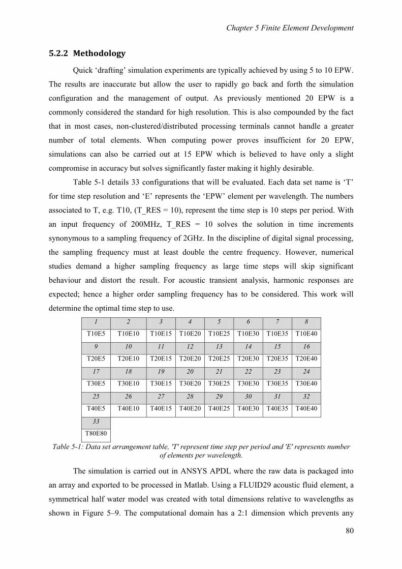
Chapter 5 Finite Element Development
80
5.2.2 Methodology
Quick ‘drafting’ simulation experiments are typically achieved by using 5 to 10 EPW.
The results are inaccurate but allow the user to rapidly go back and forth the simulation
configuration and the management of output. As previously mentioned 20 EPW is a
commonly considered the standard for high resolution. This is also compounded by the fact
that in most cases, non-clustered/distributed processing terminals cannot handle a greater
number of total elements. When computing power proves insufficient for 20 EPW,
simulations can also be carried out at 15 EPW which is believed to have only a slight
compromise in accuracy but solves significantly faster making it highly desirable.
Table 5-1 details 33 configurations that will be evaluated. Each data set name is ‘T’
for time step resolution and ‘E’ represents the ‘EPW’ element per wavelength. The numbers
associated to T, e.g. T10, (T_RES = 10), represent the time step is 10 steps per period. With
an input frequency of 200MHz, T_RES = 10 solves the solution in time increments
synonymous to a sampling frequency of 2GHz. In the discipline of digital signal processing,
the sampling frequency must at least double the centre frequency. However, numerical
studies demand a higher sampling frequency as large time steps will skip significant
behaviour and distort the result. For acoustic transient analysis, harmonic responses are
expected; hence a higher order sampling frequency has to be considered. This work will
determine the optimal time step to use.
1 2 3 4 5 6 7 8
T10E5 T10E10 T10E15 T10E20 T10E25 T10E30 T10E35 T10E40
9 10 11 12 13 14 15 16
T20E5 T20E10 T20E15 T20E20 T20E25 T20E30 T20E35 T20E40
17 18 19 20 21 22 23 24
T30E5 T30E10 T30E15 T30E20 T30E25 T30E30 T30E35 T30E40
25 26 27 28 29 30 31 32
T40E5 T40E10 T40E15 T40E20 T40E25 T40E30 T40E35 T40E40
33
T80E80
Table 5-1: Data set arrangement table, 'T' represent time step per period and 'E' represents number
of elements per wavelength.
The simulation is carried out in ANSYS APDL where the raw data is packaged into
an array and exported to be processed in Matlab. Using a FLUID29 acoustic fluid element, a
symmetrical half water model was created with total dimensions relative to wavelengths as
shown in Figure 5–9. The computational domain has a 2:1 dimension which prevents any
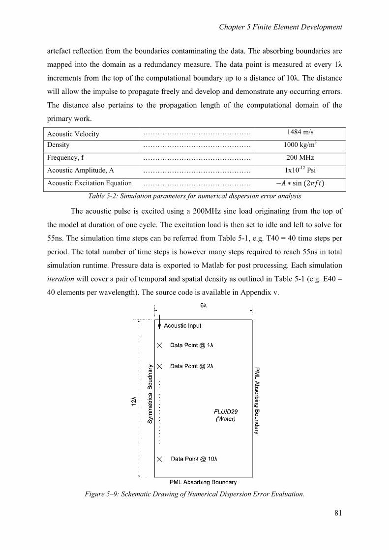
Chapter 5 Finite Element Development
81
artefact reflection from the boundaries contaminating the data. The absorbing boundaries are
mapped into the domain as a redundancy measure. The data point is measured at every 1λ
increments from the top of the computational boundary up to a distance of 10λ. The distance
will allow the impulse to propagate freely and develop and demonstrate any occurring errors.
The distance also pertains to the propagation length of the computational domain of the
primary work.
Acoustic Velocity ……………………………………… 1484 m/s
Density ……………………………………… 1000 kg/m3
Frequency, f ……………………………………… 200 MHz
Acoustic Amplitude, A ……………………………………… 1x10-12
Psi
Acoustic Excitation Equation ………………………………………
Table 5-2: Simulation parameters for numerical dispersion error analysis
The acoustic pulse is excited using a 200MHz sine load originating from the top of
the model at duration of one cycle. The excitation load is then set to idle and left to solve for
55ns. The simulation time steps can be referred from Table 5-1, e.g. T40 = 40 time steps per
period. The total number of time steps is however many steps required to reach 55ns in total
simulation runtime. Pressure data is exported to Matlab for post processing. Each simulation
iteration will cover a pair of temporal and spatial density as outlined in Table 5-1 (e.g. E40 =
40 elements per wavelength). The source code is available in Appendix v.
Figure 5–9: Schematic Drawing of Numerical Dispersion Error Evaluation.
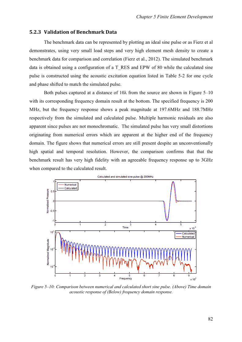
Chapter 5 Finite Element Development
82
5.2.3 Validation of Benchmark Data
The benchmark data can be represented by plotting an ideal sine pulse or as Fierz et al
demonstrates, using very small load steps and very high element mesh density to create a
benchmark data for comparison and correlation (Fierz et al., 2012). The simulated benchmark
data is obtained using a configuration of a T_RES and EPW of 80 while the calculated sine
pulse is constructed using the acoustic excitation equation listed in Table 5-2 for one cycle
and phase shifted to match the simulated pulse.
Both pulses captured at a distance of 10λ from the source are shown in Figure 5–10
with its corresponding frequency domain result at the bottom. The specified frequency is 200
MHz, but the frequency response shows a peak magnitude at 197.6MHz and 188.7MHz
respectively from the simulated and calculated pulse. Multiple harmonic residuals are also
apparent since pulses are not monochromatic. The simulated pulse has very small distortions
originating from numerical errors which are apparent at the higher end of the frequency
domain. The figure shows that numerical errors are still present despite an unconventionally
high spatial and temporal resolution. However, the comparison confirms that that the
benchmark result has very high fidelity with an agreeable frequency response up to 3GHz
when compared to the calculated result.
Figure 5–10: Comparison between numerical and calculated short sine pulse. (Above) Time domain
acoustic response of (Below) frequency domain response.
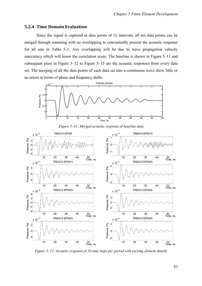
Chapter 5 Finite Element Development
83
5.2.4 Time Domain Evaluation
Since the signal is captured at data points of 1λ intervals, all ten data points can be
merged through summing with no overlapping to conveniently present the acoustic response
for all sets in Table 5-1. Any overlapping will be due to wave propagation velocity
inaccuracy which will lower the correlation score. The baseline is shown in Figure 5–11 and
subsequent plots in Figure 5–12 to Figure 5–15 are the acoustic responses from every data
set. The merging of all the data points of each data set into a continuous wave show little or
no errors in terms of phase and frequency shifts.
Figure 5–11: Merged acoustic response of baseline data
Figure 5–12: Acoustic response at 10 time steps per period with varying element density
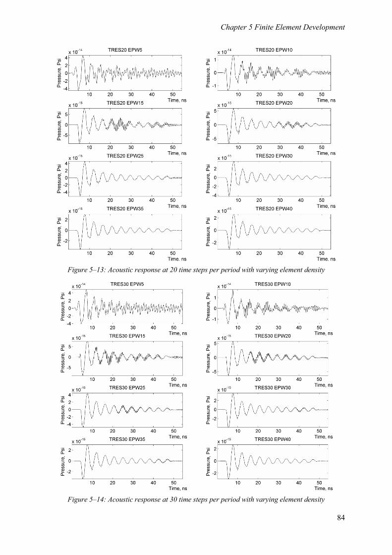
Chapter 5 Finite Element Development
84
Figure 5–13: Acoustic response at 20 time steps per period with varying element density
Figure 5–14: Acoustic response at 30 time steps per period with varying element density
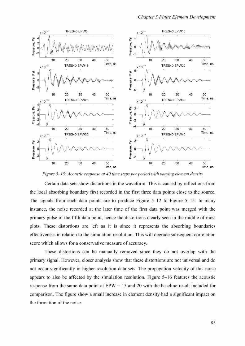
Chapter 5 Finite Element Development
85
Figure 5–15: Acoustic response at 40 time steps per period with varying element density
Certain data sets show distortions in the waveform. This is caused by reflections from
the local absorbing boundary first recorded in the first three data points close to the source.
The signals from each data points are to produce Figure 5–12 to Figure 5–15. In many
instance, the noise recorded at the later time of the first data point was merged with the
primary pulse of the fifth data point, hence the distortions clearly seen in the middle of most
plots. These distortions are left as it is since it represents the absorbing boundaries
effectiveness in relation to the simulation resolution. This will degrade subsequent correlation
score which allows for a conservative measure of accuracy.
These distortions can be manually removed since they do not overlap with the
primary signal. However, closer analysis show that these distortions are not universal and do
not occur significantly in higher resolution data sets. The propagation velocity of this noise
appears to also be affected by the simulation resolution. Figure 5–16 features the acoustic
response from the same data point at EPW = 15 and 20 with the baseline result included for
comparison. The figure show a small increase in element density had a significant impact on
the formation of the noise.
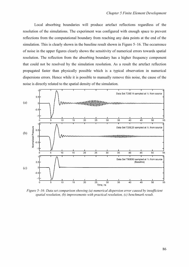
Chapter 5 Finite Element Development
86
Local absorbing boundaries will produce artefact reflections regardless of the
resolution of the simulations. The experiment was configured with enough space to prevent
reflections from the computational boundary from reaching any data points at the end of the
simulation. This is clearly shown in the baseline result shown in Figure 5–16. The occurrence
of noise in the upper figures clearly shows the sensitivity of numerical errors towards spatial
resolution. The reflection from the absorbing boundary has a higher frequency component
that could not be resolved by the simulation resolution. As a result the artefact reflection
propagated faster than physically possible which is a typical observation in numerical
dispersions errors. Hence while it is possible to manually remove this noise, the cause of the
noise is directly related to the spatial density of the simulation.
(a)
(b)
(c)
Figure 5–16: Data set comparison showing (a) numerical dispersion error caused by insufficient
spatial resolution, (b) improvements with practical resolution, (c) benchmark result.
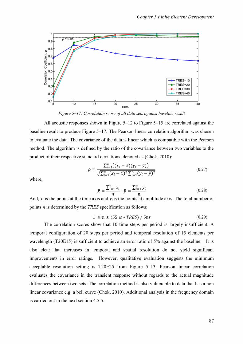
Chapter 5 Finite Element Development
87
Figure 5–17: Correlation score of all data sets against baseline result
All acoustic responses shown in Figure 5–12 to Figure 5–15 are correlated against the
baseline result to produce Figure 5–17. The Pearson linear correlation algorithm was chosen
to evaluate the data. The covariance of the data is linear which is compatible with the Pearson
method. The algorithm is defined by the ratio of the covariance between two variables to the
product of their respective standard deviations, denoted as (Chok, 2010);
(0.27)
where,
(0.28)
And, xi is the points at the time axis and yi is the points at amplitude axis. The total number of
points n is determined by the TRES specification as follows;
(0.29)
The correlation scores show that 10 time steps per period is largely insufficient. A
temporal configuration of 20 steps per period and temporal resolution of 15 elements per
wavelength (T20E15) is sufficient to achieve an error ratio of 5% against the baseline. It is
also clear that increases in temporal and spatial resolution do not yield significant
improvements in error ratings. However, qualitative evaluation suggests the minimum
acceptable resolution setting is T20E25 from Figure 5–13. Pearson linear correlation
evaluates the covariance in the transient response without regards to the actual magnitude
differences between two sets. The correlation method is also vulnerable to data that has a non
linear covariance e.g. a bell curve (Chok, 2010). Additional analysis in the frequency domain
is carried out in the next section 4.5.5.
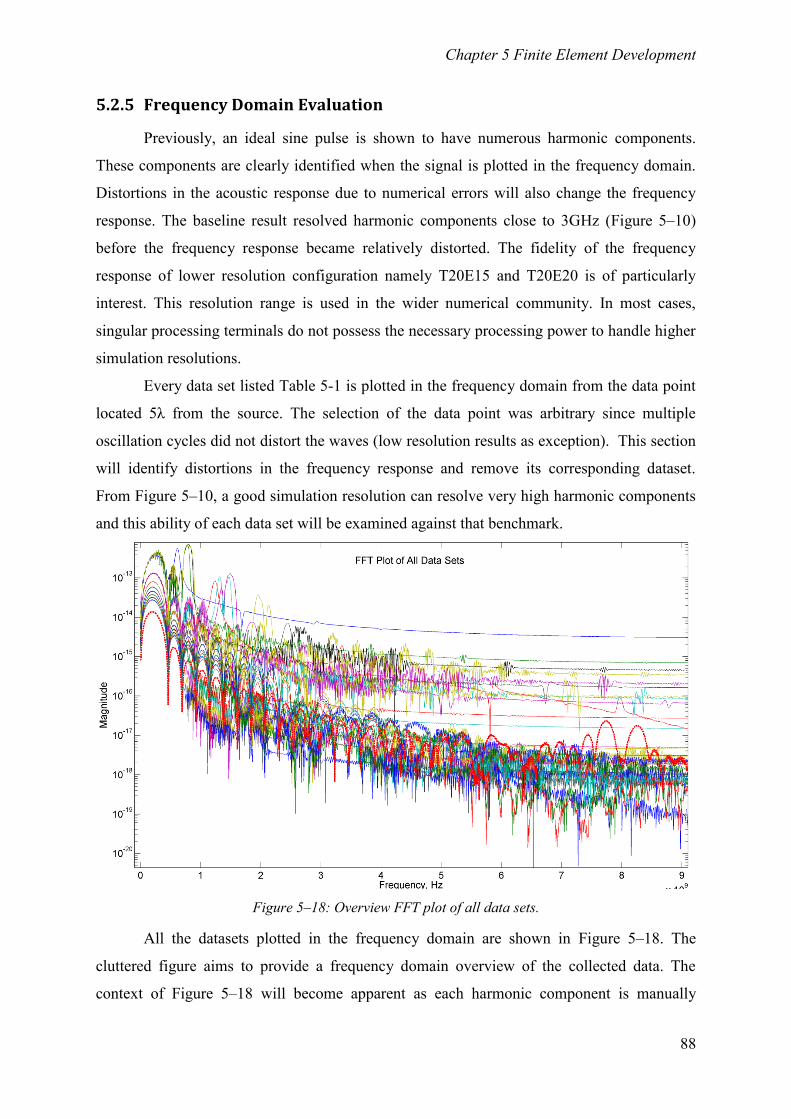
Chapter 5 Finite Element Development
88
5.2.5 Frequency Domain Evaluation
Previously, an ideal sine pulse is shown to have numerous harmonic components.
These components are clearly identified when the signal is plotted in the frequency domain.
Distortions in the acoustic response due to numerical errors will also change the frequency
response. The baseline result resolved harmonic components close to 3GHz (Figure 5–10)
before the frequency response became relatively distorted. The fidelity of the frequency
response of lower resolution configuration namely T20E15 and T20E20 is of particularly
interest. This resolution range is used in the wider numerical community. In most cases,
singular processing terminals do not possess the necessary processing power to handle higher
simulation resolutions.
Every data set listed Table 5-1 is plotted in the frequency domain from the data point
located 5λ from the source. The selection of the data point was arbitrary since multiple
oscillation cycles did not distort the waves (low resolution results as exception). This section
will identify distortions in the frequency response and remove its corresponding dataset.
From Figure 5–10, a good simulation resolution can resolve very high harmonic components
and this ability of each data set will be examined against that benchmark.
Figure 5–18: Overview FFT plot of all data sets.
All the datasets plotted in the frequency domain are shown in Figure 5–18. The
cluttered figure aims to provide a frequency domain overview of the collected data. The
context of Figure 5–18 will become apparent as each harmonic component is manually
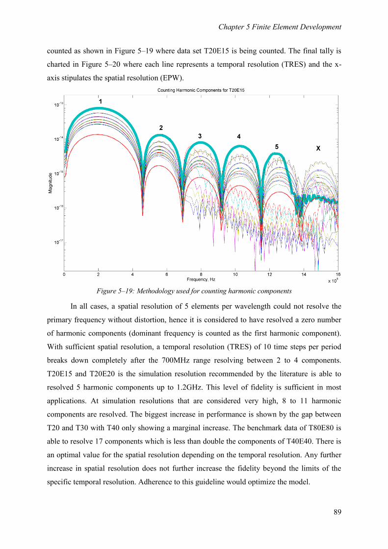
Chapter 5 Finite Element Development
89
counted as shown in Figure 5–19 where data set T20E15 is being counted. The final tally is
charted in Figure 5–20 where each line represents a temporal resolution (TRES) and the x-
axis stipulates the spatial resolution (EPW).
Figure 5–19: Methodology used for counting harmonic components
In all cases, a spatial resolution of 5 elements per wavelength could not resolve the
primary frequency without distortion, hence it is considered to have resolved a zero number
of harmonic components (dominant frequency is counted as the first harmonic component).
With sufficient spatial resolution, a temporal resolution (TRES) of 10 time steps per period
breaks down completely after the 700MHz range resolving between 2 to 4 components.
T20E15 and T20E20 is the simulation resolution recommended by the literature is able to
resolved 5 harmonic components up to 1.2GHz. This level of fidelity is sufficient in most
applications. At simulation resolutions that are considered very high, 8 to 11 harmonic
components are resolved. The biggest increase in performance is shown by the gap between
T20 and T30 with T40 only showing a marginal increase. The benchmark data of T80E80 is
able to resolve 17 components which is less than double the components of T40E40. There is
an optimal value for the spatial resolution depending on the temporal resolution. Any further
increase in spatial resolution does not further increase the fidelity beyond the limits of the
specific temporal resolution. Adherence to this guideline would optimize the model.
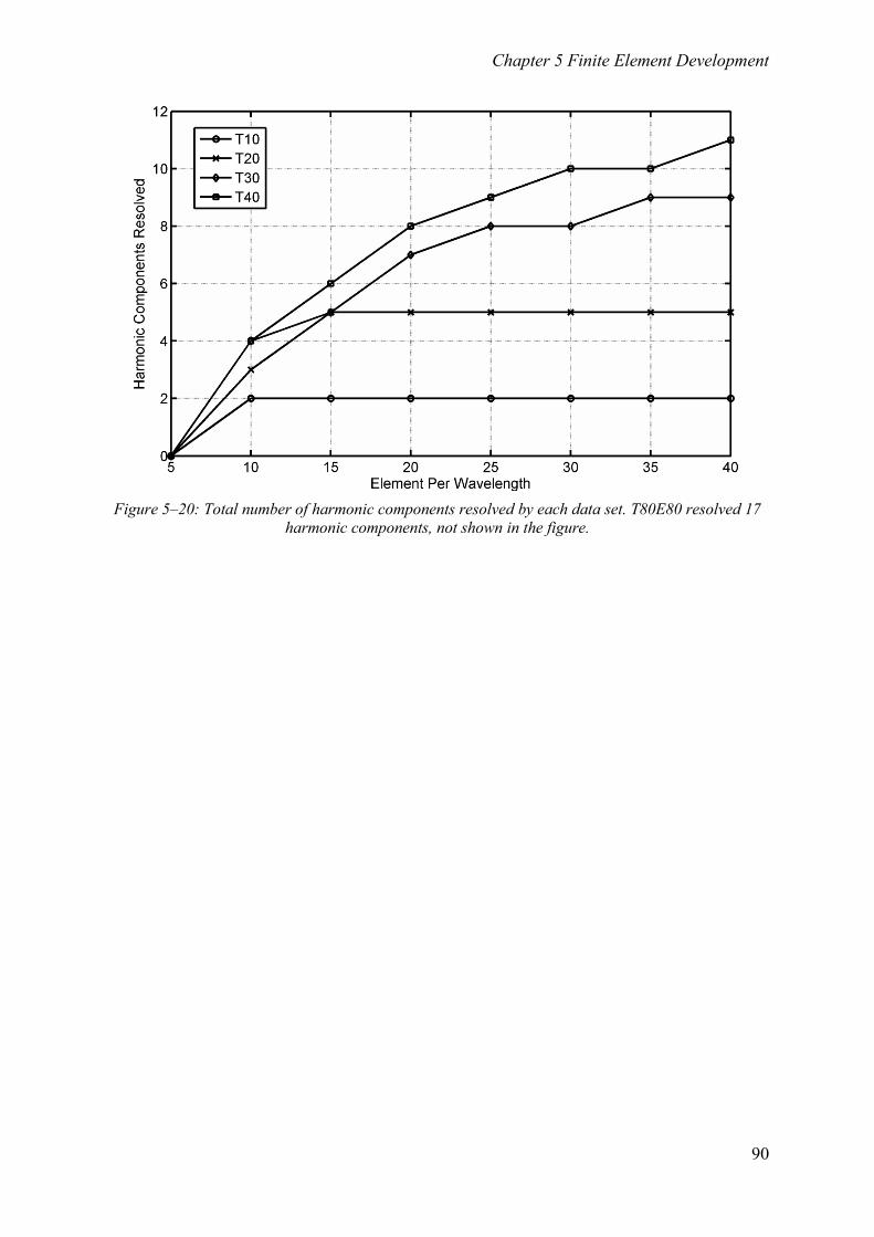
Chapter 5 Finite Element Development
90
Figure 5–20: Total number of harmonic components resolved by each data set. T80E80 resolved 17
harmonic components, not shown in the figure.
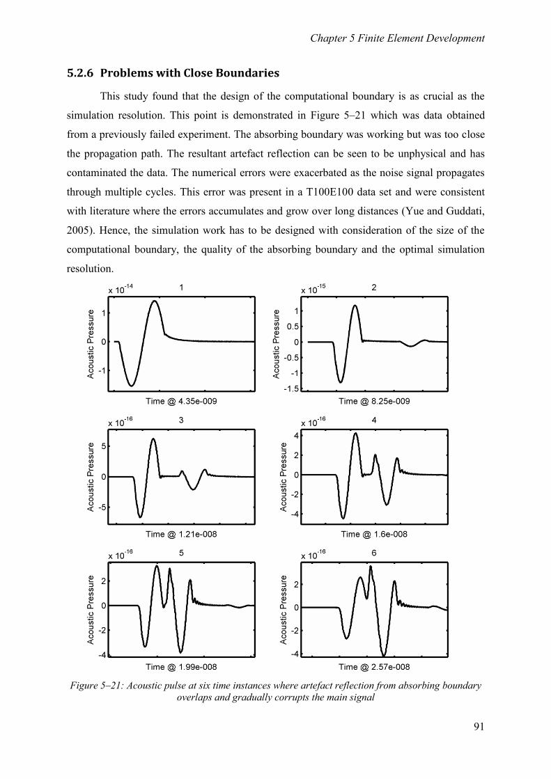
Chapter 5 Finite Element Development
91
5.2.6 Problems with Close Boundaries
This study found that the design of the computational boundary is as crucial as the
simulation resolution. This point is demonstrated in Figure 5–21 which was data obtained
from a previously failed experiment. The absorbing boundary was working but was too close
the propagation path. The resultant artefact reflection can be seen to be unphysical and has
contaminated the data. The numerical errors were exacerbated as the noise signal propagates
through multiple cycles. This error was present in a T100E100 data set and were consistent
with literature where the errors accumulates and grow over long distances (Yue and Guddati,
2005). Hence, the simulation work has to be designed with consideration of the size of the
computational boundary, the quality of the absorbing boundary and the optimal simulation
resolution.
Figure 5–21: Acoustic pulse at six time instances where artefact reflection from absorbing boundary
overlaps and gradually corrupts the main signal
Chapter 5 Finite Element Development
92
5.2.7 Chapter Conclusion
The aim was to obtain the optimal combination between computational load and
numerical accuracy. Any practical simulation approach will have to consider a marginal but
measurable amount of error in the simulation. The resolution setting used in most literature
has a correlation coefficient above 0.95 for a spatial density (EPW) of 15 elements per
wavelength and close to 0.99 when the EPW is 20 when compared against the baseline result.
The results also show no significant improvement in numerical errors above this resolution
setting. Ideally, all simulations would be carried out with a TRES and EPW of 80 as shown
by the baseline, but the quadratic increase in computational cost is highly prohibitive. With
stand alone terminals, T20E20 is barely manageable even with multi-core processing. If noise
that arises from the interaction with the computational boundary is managed, the resolution
setting can be as low as T20E15. This noise is the typical manifestation of numerical
dispersion errors. The oscillation amplitude of harmonic components as well as the
propagation velocity experiences an unphysical increase. Increasing the temporal resolution
would improve the resolution of the harmonic components at a linear increase in
computational cost. It appears the spatial density is related to the distortion of the frequency
response while the temporal resolution affects the fidelity of the harmonic components. Since
short pulses contain many high frequency components, the qualities of a short pulse are more
dependent on the temporal resolution.
Chapter 6 Scanning Microscale Virtual Transducer
93
Chapter 6
Scanning Microscale Virtual
Transducer
Chapter 6 Scanning Microscale Virtual Transducer
94
6 Scanning Microscale Virtual Transducer
This chapter examines the finite element methodology used for the modelling Flip
Chip – AMI image acquisition. There are two concerns with any finite element work;
accuracy and cost. Accuracy can be split into two categories. First, the inherent error
introduced by the weak form equations used to solve finite element problems. The
approximation errors need to be small enough to be negligible. The second problem with
accuracy is the configuration of the finite element software. A valid problem when a user
does not appreciate the subtle differences between each configuration profile and choices.
Then we arrive at the problem of computation cost which represents a significant barrier. To
overcome this, various approaches and compromise are deployed. The effects of these cost
reduction techniques are not always well documented. Now it becomes important to validate
the configuration to ensure the cost management strategy do not affect the desired accuracy.
6.1 Modelling of Acoustic Micro Imaging for Flip Chip Packages.
In practical AMI systems, the sample is normally submerged in water to reduce
impedance mismatch as the transducer produces pulse echoes which propagate along the
longitudinal axis through the sample. When the pulse echo encounters an interface between
two differing materials, a reflection is produced due to the impedance mismatch. This
reflection is then picked up and recorded by the same transducer. The transducer then moves
a lateral step (typically a few micrometers) and repeats the process. The resultant data is
gated in related to time to obtain information at the desired interface or depth of the sample.
Understandably, the acoustic pulse propagation mechanism within the solid specimen cannot
be observed directly.
Numerical models can accurately approximate the intra sample acoustic mechanisms
and various other physical phenomena. The key challenge however is the management of
computational resources. This chapter will examine the strategies and configuration
developed to perform acoustic transient analysis within the computational budget.
The numerical model is configured to imitate the AMI scanning mechanism. Each
transducer position will require a simulation restart which linearly increases computational
cost proportional to the scanning resolution. Each simulation restart will be called an
“iteration” followed by a number which reflects the transducer position off the central axis of
the solder bump (this keyword will be used extensively in the next chapter). The strategy to
lower total number of elements is accomplished by dynamically adjusting the resolution
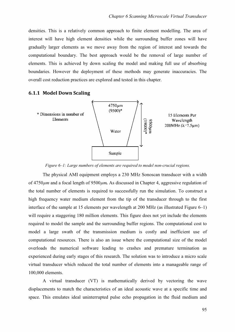
Chapter 6 Scanning Microscale Virtual Transducer
95
densities. This is a relatively common approach to finite element modelling. The area of
interest will have high element densities while the surrounding buffer zones will have
gradually larger elements as we move away from the region of interest and towards the
computational boundary. The best approach would be the removal of large number of
elements. This is achieved by down scaling the model and making full use of absorbing
boundaries. However the deployment of these methods may generate inaccuracies. The
overall cost reduction practices are explored and tested in this chapter.
6.1.1 Model Down Scaling
Figure 6–1: Large numbers of elements are required to model non-crucial regions.
The physical AMI equipment employs a 230 MHz Sonoscan transducer with a width
of 4750µm and a focal length of 9500µm. As discussed in Chapter 4, aggressive regulation of
the total number of elements is required to successfully run the simulation. To construct a
high frequency water medium element from the tip of the transducer through to the first
interface of the sample at 15 elements per wavelength at 200 MHz (as illustrated Figure 6–1)
will require a staggering 180 million elements. This figure does not yet include the elements
required to model the sample and the surrounding buffer regions. The computational cost to
model a large swath of the transmission medium is costly and inefficient use of
computational resources. There is also an issue where the computational size of the model
overloads the numerical software leading to crashes and premature termination as
experienced during early stages of this research. The solution was to introduce a micro scale
virtual transducer which reduced the total number of elements into a manageable range of
100,000 elements.
A virtual transducer (VT) is mathematically derived by vectoring the wave
displacements to match the characteristics of an ideal acoustic wave at a specific time and
space. This emulates ideal uninterrupted pulse echo propagation in the fluid medium and
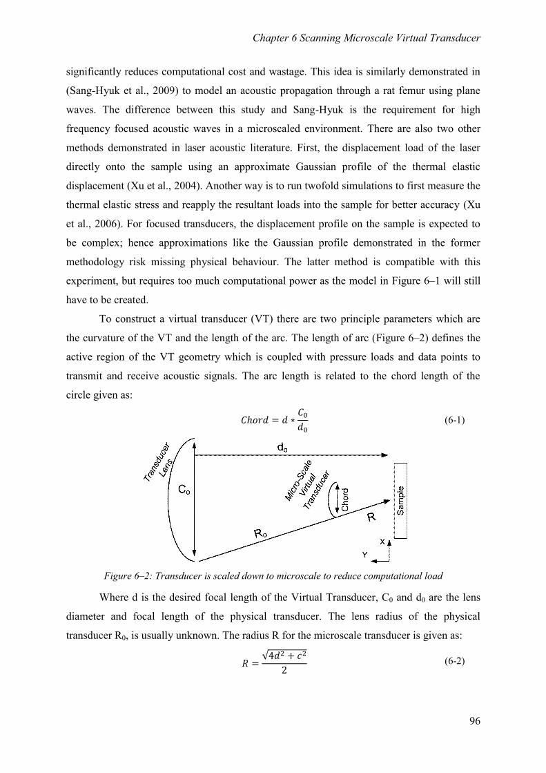
Chapter 6 Scanning Microscale Virtual Transducer
96
significantly reduces computational cost and wastage. This idea is similarly demonstrated in
(Sang-Hyuk et al., 2009) to model an acoustic propagation through a rat femur using plane
waves. The difference between this study and Sang-Hyuk is the requirement for high
frequency focused acoustic waves in a microscaled environment. There are also two other
methods demonstrated in laser acoustic literature. First, the displacement load of the laser
directly onto the sample using an approximate Gaussian profile of the thermal elastic
displacement (Xu et al., 2004). Another way is to run twofold simulations to first measure the
thermal elastic stress and reapply the resultant loads into the sample for better accuracy (Xu
et al., 2006). For focused transducers, the displacement profile on the sample is expected to
be complex; hence approximations like the Gaussian profile demonstrated in the former
methodology risk missing physical behaviour. The latter method is compatible with this
experiment, but requires too much computational power as the model in Figure 6–1 will still
have to be created.
To construct a virtual transducer (VT) there are two principle parameters which are
the curvature of the VT and the length of the arc. The length of arc (Figure 6–2) defines the
active region of the VT geometry which is coupled with pressure loads and data points to
transmit and receive acoustic signals. The arc length is related to the chord length of the
circle given as:
(6-1)
Figure 6–2: Transducer is scaled down to microscale to reduce computational load
Where d is the desired focal length of the Virtual Transducer, C0 and d0 are the lens
diameter and focal length of the physical transducer. The lens radius of the physical
transducer R0, is usually unknown. The radius R for the microscale transducer is given as:
(6-2)
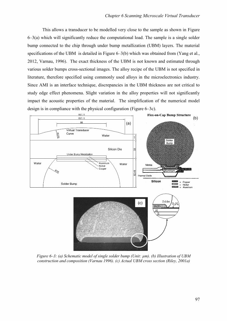
Chapter 6 Scanning Microscale Virtual Transducer
97
This allows a transducer to be modelled very close to the sample as shown in Figure
6–3(a) which will significantly reduce the computational load. The sample is a single solder
bump connected to the chip through under bump metallization (UBM) layers. The material
specifications of the UBM is detailed in Figure 6–3(b) which was obtained from (Yang et al.,
2012, Varnau, 1996). The exact thickness of the UBM is not known and estimated through
various solder bumps cross-sectional images. The alloy recipe of the UBM is not specified in
literature, therefore specified using commonly used alloys in the microelectronics industry.
Since AMI is an interface technique, discrepancies in the UBM thickness are not critical to
study edge effect phenomena. Slight variation in the alloy properties will not significantly
impact the acoustic properties of the material. The simplification of the numerical model
design is in compliance with the physical configuration (Figure 6–3c).
Figure 6–3: (a) Schematic model of single solder bump (Unit: µm). (b) Illustration of UBM
construction and composition (Varnau 1996). (c) Actual UBM cross section (Riley, 2001a)
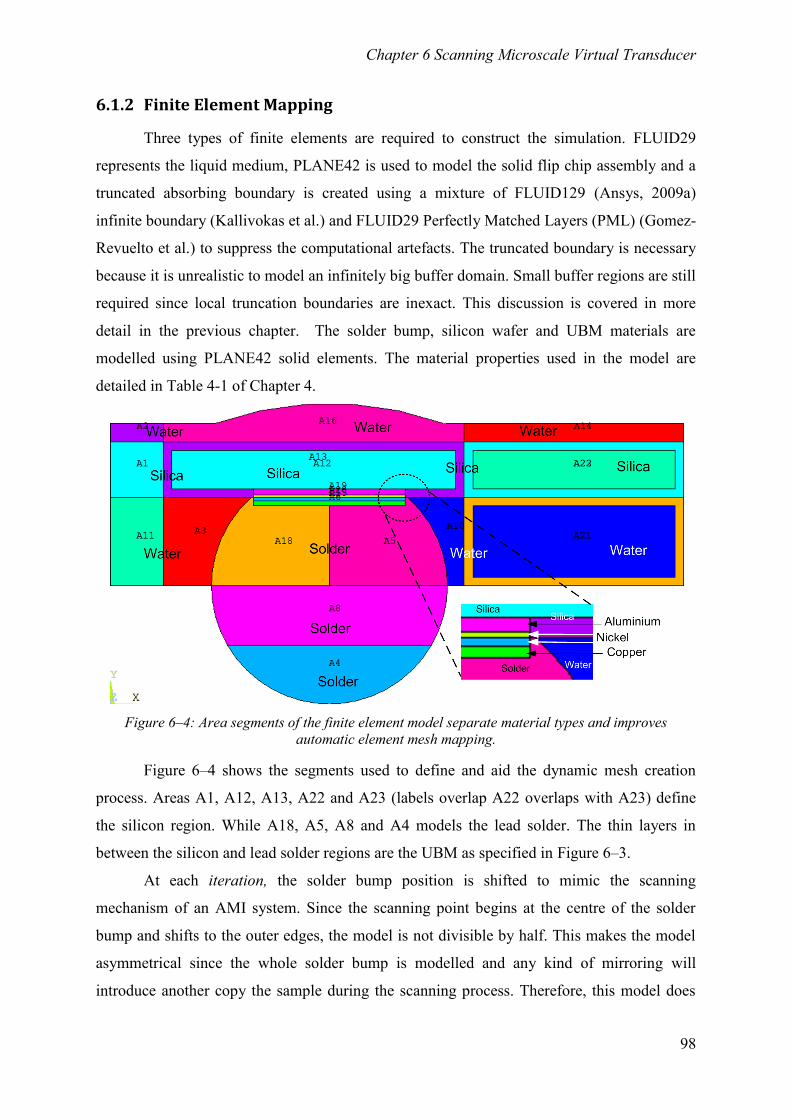
Chapter 6 Scanning Microscale Virtual Transducer
98
6.1.2 Finite Element Mapping
Three types of finite elements are required to construct the simulation. FLUID29
represents the liquid medium, PLANE42 is used to model the solid flip chip assembly and a
truncated absorbing boundary is created using a mixture of FLUID129 (Ansys, 2009a)
infinite boundary (Kallivokas et al.) and FLUID29 Perfectly Matched Layers (PML) (Gomez-
Revuelto et al.) to suppress the computational artefacts. The truncated boundary is necessary
because it is unrealistic to model an infinitely big buffer domain. Small buffer regions are still
required since local truncation boundaries are inexact. This discussion is covered in more
detail in the previous chapter. The solder bump, silicon wafer and UBM materials are
modelled using PLANE42 solid elements. The material properties used in the model are
detailed in Table 4-1 of Chapter 4.
Figure 6–4: Area segments of the finite element model separate material types and improves
automatic element mesh mapping.
Figure 6–4 shows the segments used to define and aid the dynamic mesh creation
process. Areas A1, A12, A13, A22 and A23 (labels overlap A22 overlaps with A23) define
the silicon region. While A18, A5, A8 and A4 models the lead solder. The thin layers in
between the silicon and lead solder regions are the UBM as specified in Figure 6–3.
At each iteration, the solder bump position is shifted to mimic the scanning
mechanism of an AMI system. Since the scanning point begins at the centre of the solder
bump and shifts to the outer edges, the model is not divisible by half. This makes the model
asymmetrical since the whole solder bump is modelled and any kind of mirroring will
introduce another copy the sample during the scanning process. Therefore, this model does
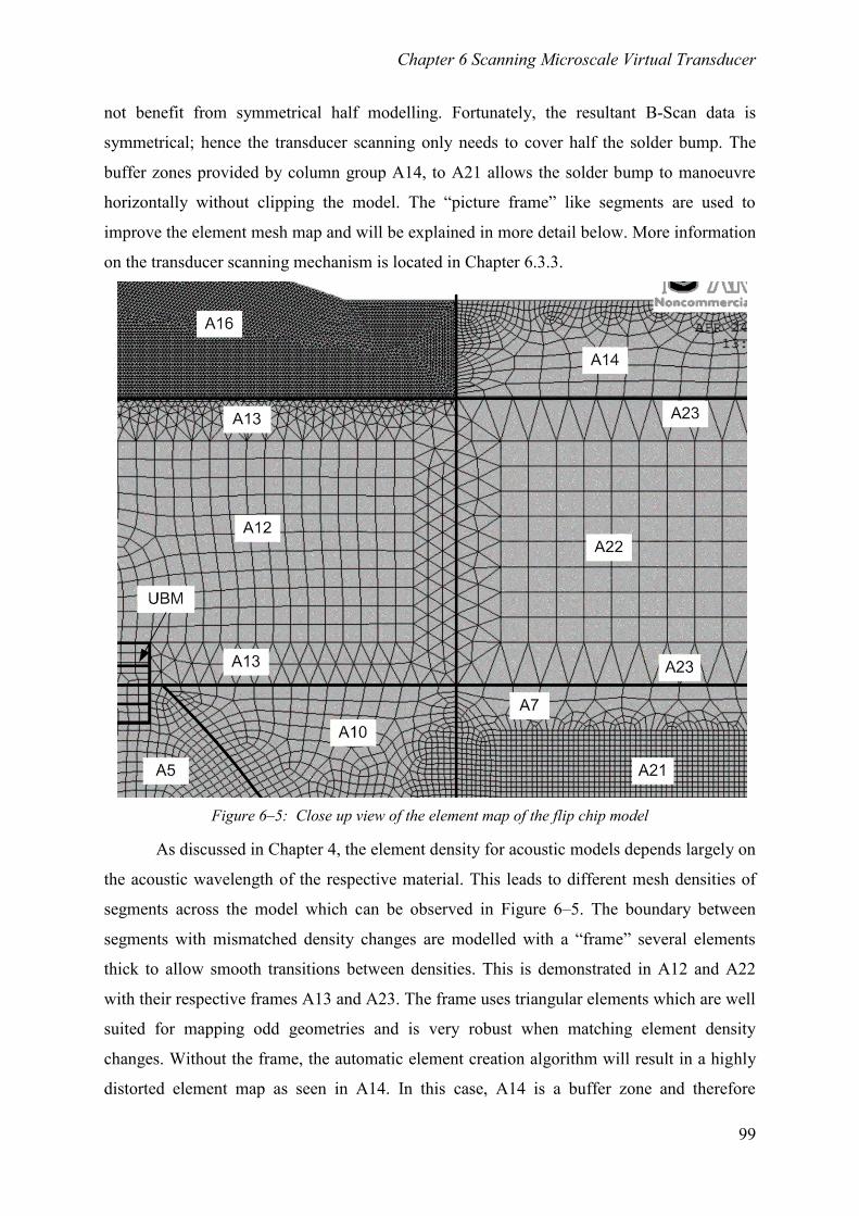
Chapter 6 Scanning Microscale Virtual Transducer
99
not benefit from symmetrical half modelling. Fortunately, the resultant B-Scan data is
symmetrical; hence the transducer scanning only needs to cover half the solder bump. The
buffer zones provided by column group A14, to A21 allows the solder bump to manoeuvre
horizontally without clipping the model. The “picture frame” like segments are used to
improve the element mesh map and will be explained in more detail below. More information
on the transducer scanning mechanism is located in Chapter 6.3.3.
Figure 6–5: Close up view of the element map of the flip chip model
As discussed in Chapter 4, the element density for acoustic models depends largely on
the acoustic wavelength of the respective material. This leads to different mesh densities of
segments across the model which can be observed in Figure 6–5. The boundary between
segments with mismatched density changes are modelled with a “frame” several elements
thick to allow smooth transitions between densities. This is demonstrated in A12 and A22
with their respective frames A13 and A23. The frame uses triangular elements which are well
suited for mapping odd geometries and is very robust when matching element density
changes. Without the frame, the automatic element creation algorithm will result in a highly
distorted element map as seen in A14. In this case, A14 is a buffer zone and therefore
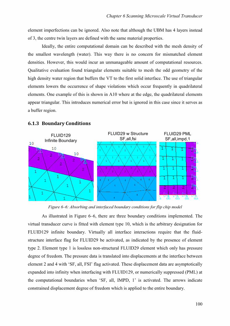
Chapter 6 Scanning Microscale Virtual Transducer
100
element imperfections can be ignored. Also note that although the UBM has 4 layers instead
of 3, the centre twin layers are defined with the same material properties.
Ideally, the entire computational domain can be described with the mesh density of
the smallest wavelength (water). This way there is no concern for mismatched element
densities. However, this would incur an unmanageable amount of computational resources.
Qualitative evaluation found triangular elements suitable to mesh the odd geometry of the
high density water region that buffers the VT to the first solid interface. The use of triangular
elements lowers the occurrence of shape violations which occur frequently in quadrilateral
elements. One example of this is shown in A10 where at the edge, the quadrilateral elements
appear triangular. This introduces numerical error but is ignored in this case since it serves as
a buffer region.
6.1.3 Boundary Conditions
FLUID129
Infinite Boundary
FLUID29 w Structure
SF,all,fsiFLUID29 PML
SF,all,impd,1
Figure 6–6: Absorbing and interfaced boundary conditions for flip chip model
As illustrated in Figure 6–6, there are three boundary conditions implemented. The
virtual transducer curve is fitted with element type 10, which is the arbitrary designation for
FLUID129 infinite boundary. Virtually all interface interactions require that the fluid-
structure interface flag for FLUID29 be activated, as indicated by the presence of element
type 2. Element type 1 is lossless non-structural FLUID29 element which only has pressure
degree of freedom. The pressure data is translated into displacements at the interface between
element 2 and 4 with ‘SF, all, FSI’ flag activated. These displacement data are asymptotically
expanded into infinity when interfacing with FLUID129, or numerically suppressed (PML) at
the computational boundaries when ‘SF, all, IMPD, 1’ is activated. The arrows indicate
constrained displacement degree of freedom which is applied to the entire boundary.
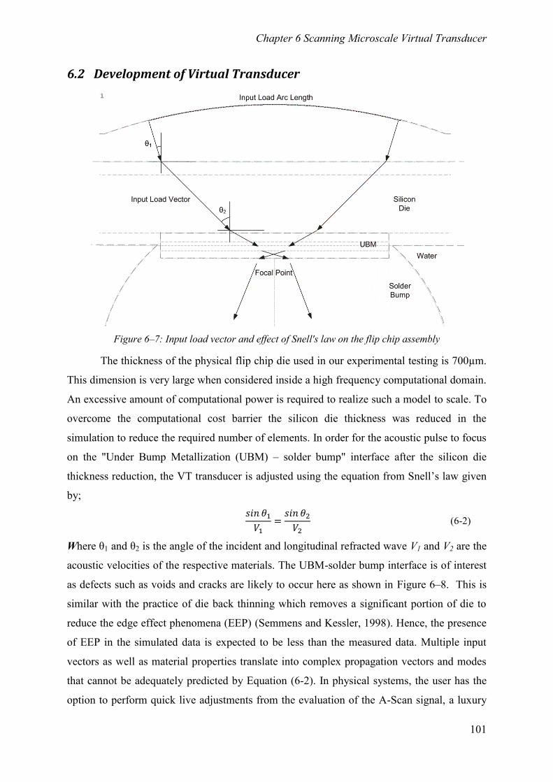
Chapter 6 Scanning Microscale Virtual Transducer
101
6.2 Development of Virtual Transducer
Figure 6–7: Input load vector and effect of Snell's law on the flip chip assembly
The thickness of the physical flip chip die used in our experimental testing is 700µm.
This dimension is very large when considered inside a high frequency computational domain.
An excessive amount of computational power is required to realize such a model to scale. To
overcome the computational cost barrier the silicon die thickness was reduced in the
simulation to reduce the required number of elements. In order for the acoustic pulse to focus
on the "Under Bump Metallization (UBM) – solder bump" interface after the silicon die
thickness reduction, the VT transducer is adjusted using the equation from Snell’s law given
by;
(6-2)
Where θ1 and θ2 is the angle of the incident and longitudinal refracted wave V1 and V2 are the
acoustic velocities of the respective materials. The UBM-solder bump interface is of interest
as defects such as voids and cracks are likely to occur here as shown in Figure 6–8. This is
similar with the practice of die back thinning which removes a significant portion of die to
reduce the edge effect phenomena (EEP) (Semmens and Kessler, 1998). Hence, the presence
of EEP in the simulated data is expected to be less than the measured data. Multiple input
vectors as well as material properties translate into complex propagation vectors and modes
that cannot be adequately predicted by Equation (6-2). In physical systems, the user has the
option to perform quick live adjustments from the evaluation of the A-Scan signal, a luxury
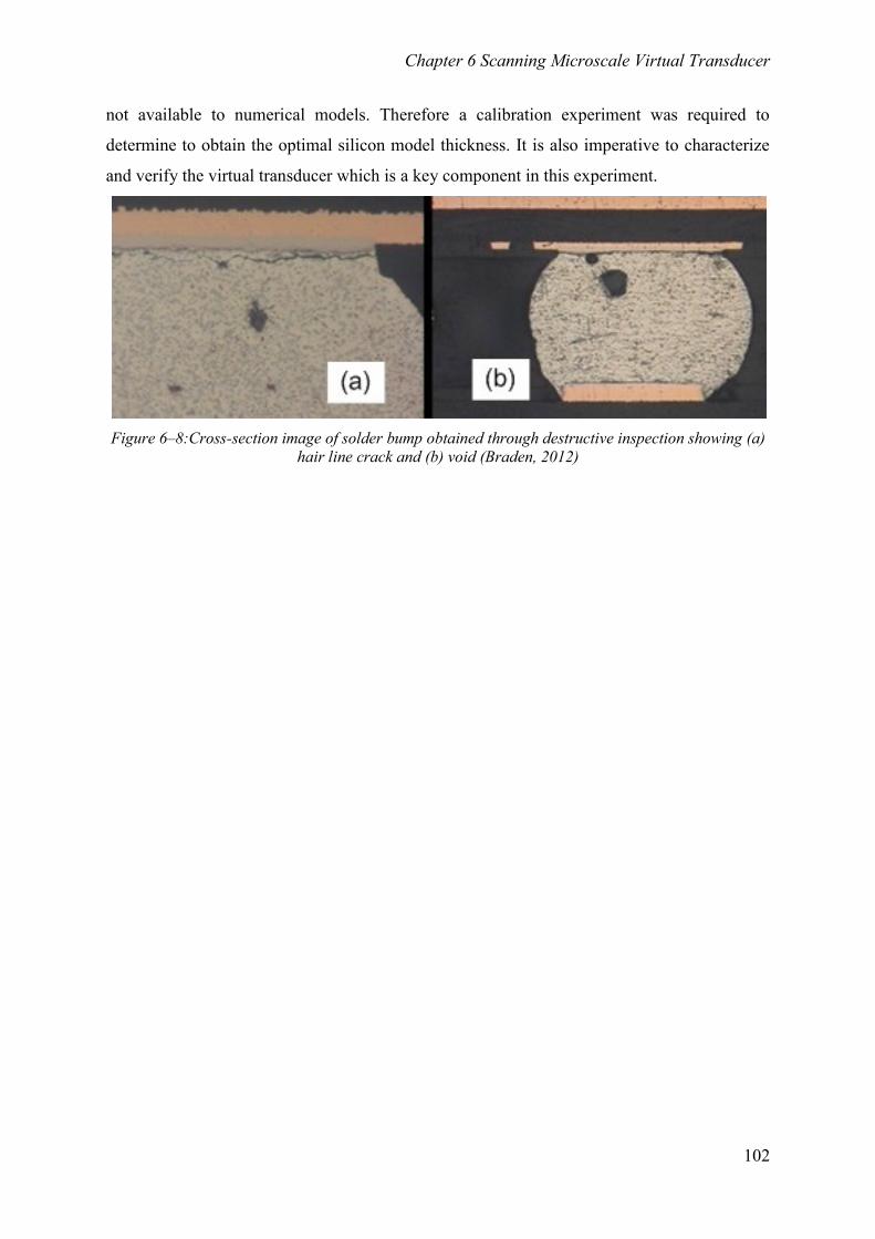
Chapter 6 Scanning Microscale Virtual Transducer
102
not available to numerical models. Therefore a calibration experiment was required to
determine to obtain the optimal silicon model thickness. It is also imperative to characterize
and verify the virtual transducer which is a key component in this experiment.
Figure 6–8:Cross-section image of solder bump obtained through destructive inspection showing (a)
hair line crack and (b) void (Braden, 2012)
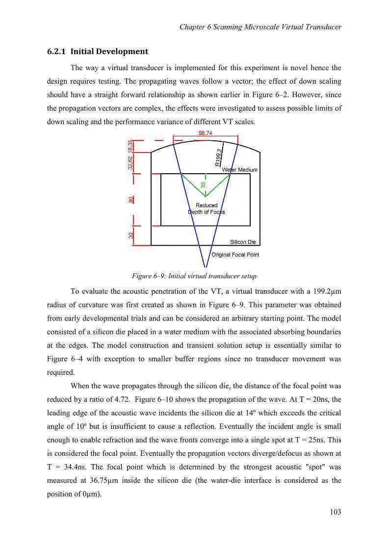
Chapter 6 Scanning Microscale Virtual Transducer
103
6.2.1 Initial Development
The way a virtual transducer is implemented for this experiment is novel hence the
design requires testing. The propagating waves follow a vector; the effect of down scaling
should have a straight forward relationship as shown earlier in Figure 6–2. However, since
the propagation vectors are complex, the effects were investigated to assess possible limits of
down scaling and the performance variance of different VT scales.
Figure 6–9: Initial virtual transducer setup
To evaluate the acoustic penetration of the VT, a virtual transducer with a 199.2µm
radius of curvature was first created as shown in Figure 6–9. This parameter was obtained
from early developmental trials and can be considered an arbitrary starting point. The model
consisted of a silicon die placed in a water medium with the associated absorbing boundaries
at the edges. The model construction and transient solution setup is essentially similar to
Figure 6–4 with exception to smaller buffer regions since no transducer movement was
required.
When the wave propagates through the silicon die, the distance of the focal point was
reduced by a ratio of 4.72. Figure 6–10 shows the propagation of the wave. At T = 20ns, the
leading edge of the acoustic wave incidents the silicon die at 14º which exceeds the critical
angle of 10º but is insufficient to cause a reflection. Eventually the incident angle is small
enough to enable refraction and the wave fronts converge into a single spot at T = 25ns. This
is considered the focal point. Eventually the propagation vectors diverge/defocus as shown at
T = 34.4ns. The focal point which is determined by the strongest acoustic "spot" was
measured at 36.75µm inside the silicon die (the water-die interface is considered as the
position of 0µm).
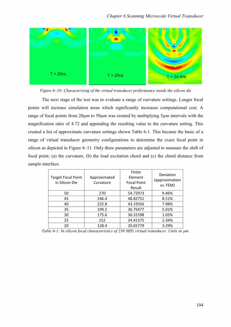
Chapter 6 Scanning Microscale Virtual Transducer
104
T = 34.4nsT = 25nsT = 20ns
Figure 6–10: Characterizing of the virtual transducer performance inside the silicon die
The next stage of the test was to evaluate a range of curvature settings. Longer focal
points will increase simulation areas which significantly increases computational cost. A
range of focal points from 20µm to 50µm was created by multiplying 5µm intervals with the
magnification ratio of 4.72 and appending the resulting value to the curvature setting. This
created a list of approximate curvature settings shown Table 6-1. This became the basic of a
range of virtual transducer geometry configurations to determine the exact focal point in
silicon as depicted in Figure 6–11. Only three parameters are adjusted to measure the shift of
focal point; (a) the curvature, (b) the load excitation chord and (c) the chord distance from
sample interface.
Target Focal Point in Silicon Die
Approximated Curvature
Finite Element
Focal Point Result
Deviation (approximation
vs. FEM)
50 270 54.72973 9.46% 45 246.4 48.82751 8.51% 40 222.8 43.19356 7.98% 35 199.2 36.75477 5.01% 30 175.6 30.31598 1.05% 25 152 24.41375 2.34% 20 128.4 20.65779 3.29%
Table 6-1: In silicon focal characteristics of 230 MHz virtual transducer. Units in µm.
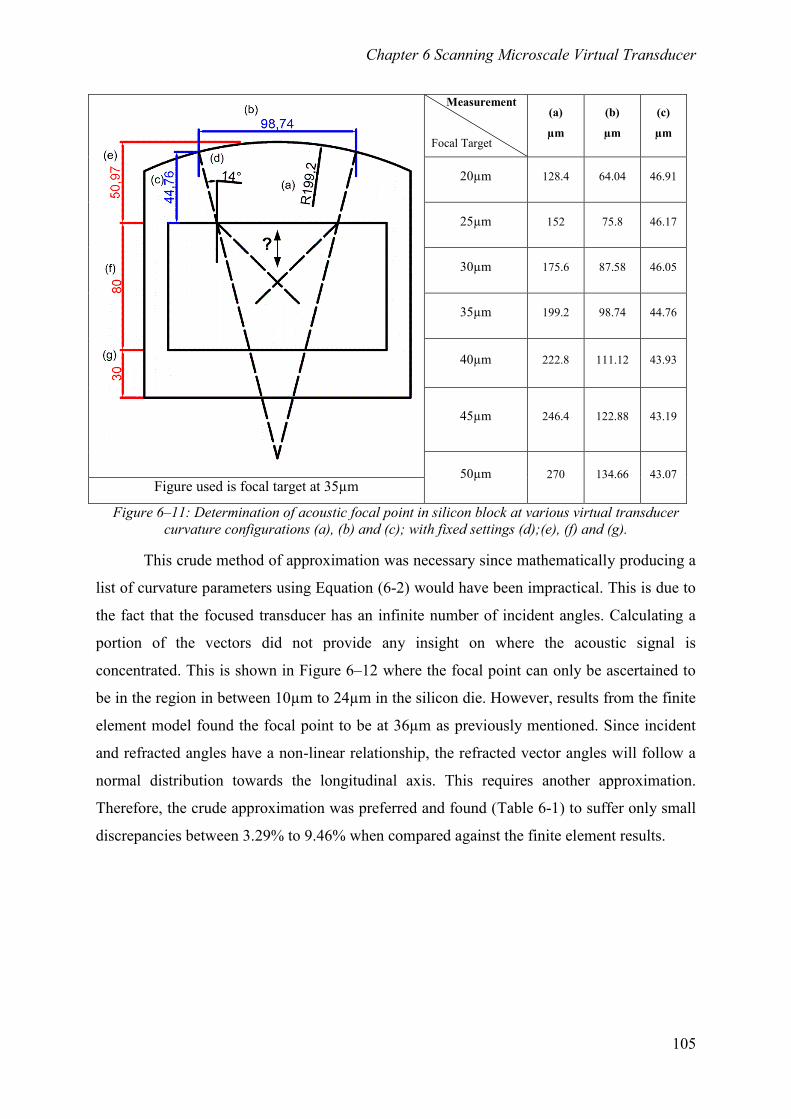
Chapter 6 Scanning Microscale Virtual Transducer
105
Measurement
Focal Target
(a)
µm
(b)
µm
(c)
µm
20µm 128.4 64.04 46.91
25µm 152 75.8 46.17
30µm 175.6 87.58 46.05
35µm 199.2 98.74 44.76
40µm 222.8 111.12 43.93
45µm 246.4 122.88 43.19
50µm 270 134.66 43.07 Figure used is focal target at 35µm
Figure 6–11: Determination of acoustic focal point in silicon block at various virtual transducer
curvature configurations (a), (b) and (c); with fixed settings (d);(e), (f) and (g).
This crude method of approximation was necessary since mathematically producing a
list of curvature parameters using Equation (6-2) would have been impractical. This is due to
the fact that the focused transducer has an infinite number of incident angles. Calculating a
portion of the vectors did not provide any insight on where the acoustic signal is
concentrated. This is shown in Figure 6–12 where the focal point can only be ascertained to
be in the region in between 10µm to 24µm in the silicon die. However, results from the finite
element model found the focal point to be at 36µm as previously mentioned. Since incident
and refracted angles have a non-linear relationship, the refracted vector angles will follow a
normal distribution towards the longitudinal axis. This requires another approximation.
Therefore, the crude approximation was preferred and found (Table 6-1) to suffer only small
discrepancies between 3.29% to 9.46% when compared against the finite element results.
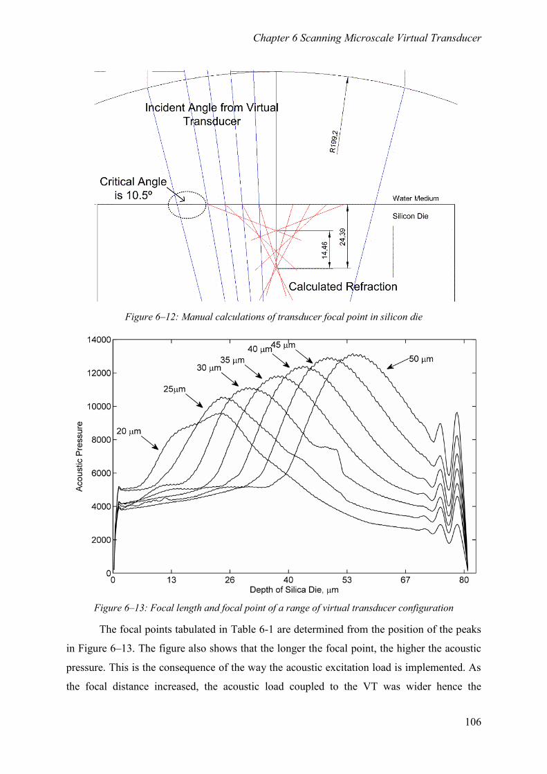
Chapter 6 Scanning Microscale Virtual Transducer
106
Figure 6–12: Manual calculations of transducer focal point in silicon die
Figure 6–13: Focal length and focal point of a range of virtual transducer configuration
The focal points tabulated in Table 6-1 are determined from the position of the peaks
in Figure 6–13. The figure also shows that the longer the focal point, the higher the acoustic
pressure. This is the consequence of the way the acoustic excitation load is implemented. As
the focal distance increased, the acoustic load coupled to the VT was wider hence the
Chapter 6 Scanning Microscale Virtual Transducer
107
acoustic signal was stronger. The difference in magnitude was the result of the numerical
technique. Analysis of results relies on relative differences between features; hence this effect
can be safely ignored.
Each curvature configuration appears to produce a consistent response with the
exception to the 20µm VT. This could be related to the focal point in the silicon being half of
the silicon wavelength of 40µm. While the cause cannot be confirmed, the data shows that
the VT has a lower scale limit. In addition, the 25µm VT has a rough response beyond the
focal point while the 30µm VT contains an anomalous bump around 50µm. The shortest
usable configuration in the curvature list appears to be the 35µm VT. This parameter is in
agreement with earlier trial and error developments. The focal depth (DOF) which is the
length in which the pulse stays in focus does not deviate significantly. As expected, VTs with
longer focal points do not appear to cause any problems.
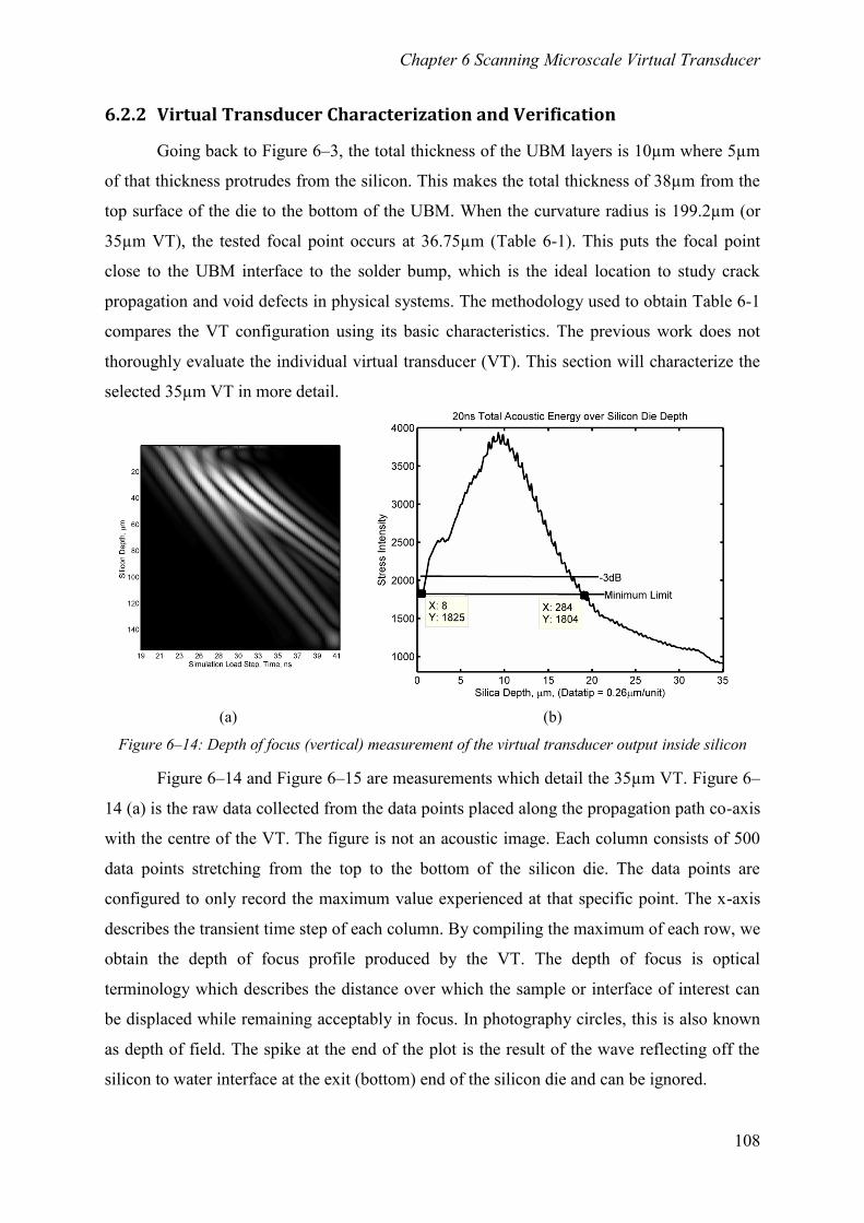
Chapter 6 Scanning Microscale Virtual Transducer
108
6.2.2 Virtual Transducer Characterization and Verification
Going back to Figure 6–3, the total thickness of the UBM layers is 10µm where 5µm
of that thickness protrudes from the silicon. This makes the total thickness of 38µm from the
top surface of the die to the bottom of the UBM. When the curvature radius is 199.2µm (or
35µm VT), the tested focal point occurs at 36.75µm (Table 6-1). This puts the focal point
close to the UBM interface to the solder bump, which is the ideal location to study crack
propagation and void defects in physical systems. The methodology used to obtain Table 6-1
compares the VT configuration using its basic characteristics. The previous work does not
thoroughly evaluate the individual virtual transducer (VT). This section will characterize the
selected 35µm VT in more detail.
(a) (b)
Figure 6–14: Depth of focus (vertical) measurement of the virtual transducer output inside silicon
Figure 6–14 and Figure 6–15 are measurements which detail the 35µm VT. Figure 6–
14 (a) is the raw data collected from the data points placed along the propagation path co-axis
with the centre of the VT. The figure is not an acoustic image. Each column consists of 500
data points stretching from the top to the bottom of the silicon die. The data points are
configured to only record the maximum value experienced at that specific point. The x-axis
describes the transient time step of each column. By compiling the maximum of each row, we
obtain the depth of focus profile produced by the VT. The depth of focus is optical
terminology which describes the distance over which the sample or interface of interest can
be displaced while remaining acceptably in focus. In photography circles, this is also known
as depth of field. The spike at the end of the plot is the result of the wave reflecting off the
silicon to water interface at the exit (bottom) end of the silicon die and can be ignored.
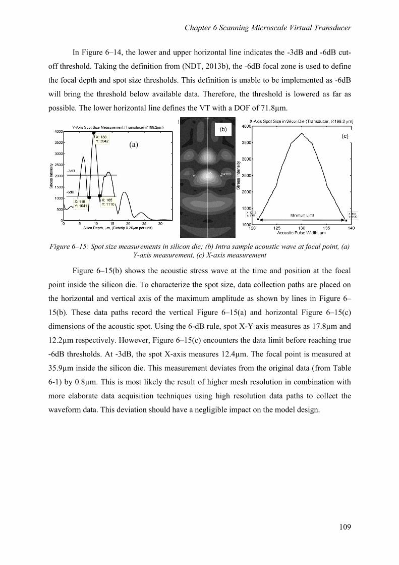
Chapter 6 Scanning Microscale Virtual Transducer
109
In Figure 6–14, the lower and upper horizontal line indicates the -3dB and -6dB cut-
off threshold. Taking the definition from (NDT, 2013b), the -6dB focal zone is used to define
the focal depth and spot size thresholds. This definition is unable to be implemented as -6dB
will bring the threshold below available data. Therefore, the threshold is lowered as far as
possible. The lower horizontal line defines the VT with a DOF of 71.8µm.
Figure 6–15: Spot size measurements in silicon die; (b) Intra sample acoustic wave at focal point, (a)
Y-axis measurement, (c) X-axis measurement
Figure 6–15(b) shows the acoustic stress wave at the time and position at the focal
point inside the silicon die. To characterize the spot size, data collection paths are placed on
the horizontal and vertical axis of the maximum amplitude as shown by lines in Figure 6–
15(b). These data paths record the vertical Figure 6–15(a) and horizontal Figure 6–15(c)
dimensions of the acoustic spot. Using the 6-dB rule, spot X-Y axis measures as 17.8µm and
12.2µm respectively. However, Figure 6–15(c) encounters the data limit before reaching true
-6dB thresholds. At -3dB, the spot X-axis measures 12.4µm. The focal point is measured at
35.9µm inside the silicon die. This measurement deviates from the original data (from Table
6-1) by 0.8µm. This is most likely the result of higher mesh resolution in combination with
more elaborate data acquisition techniques using high resolution data paths to collect the
waveform data. This deviation should have a negligible impact on the model design.
(a)
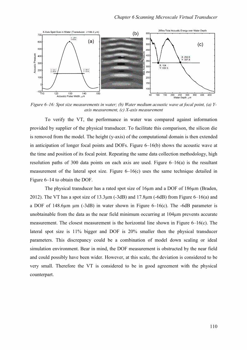
Chapter 6 Scanning Microscale Virtual Transducer
110
Figure 6–16: Spot size measurements in water; (b) Water medium acoustic wave at focal point, (a) Y-
axis measurement, (c) X-axis measurement
To verify the VT, the performance in water was compared against information
provided by supplier of the physical transducer. To facilitate this comparison, the silicon die
is removed from the model. The height (y-axis) of the computational domain is then extended
in anticipation of longer focal points and DOFs. Figure 6–16(b) shows the acoustic wave at
the time and position of its focal point. Repeating the same data collection methodology, high
resolution paths of 300 data points on each axis are used. Figure 6–16(a) is the resultant
measurement of the lateral spot size. Figure 6–16(c) uses the same technique detailed in
Figure 6–14 to obtain the DOF.
The physical transducer has a rated spot size of 16µm and a DOF of 186µm (Braden,
2012). The VT has a spot size of 13.3µm (-3dB) and 17.8µm (-6dB) from Figure 6–16(a) and
a DOF of 148.6µm µm (-3dB) in water shown in Figure 6–16(c). The -6dB parameter is
unobtainable from the data as the near field minimum occurring at 104µm prevents accurate
measurement. The closest measurement is the horizontal line shown in Figure 6–16(c). The
lateral spot size is 11% bigger and DOF is 20% smaller then the physical transducer
parameters. This discrepancy could be a combination of model down scaling or ideal
simulation environment. Bear in mind, the DOF measurement is obstructed by the near field
and could possibly have been wider. However, at this scale, the deviation is considered to be
very small. Therefore the VT is considered to be in good agreement with the physical
counterpart.
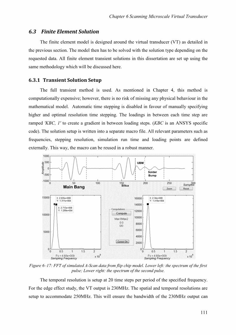
Chapter 6 Scanning Microscale Virtual Transducer
111
6.3 Finite Element Solution
The finite element model is designed around the virtual transducer (VT) as detailed in
the previous section. The model then has to be solved with the solution type depending on the
requested data. All finite element transient solutions in this dissertation are set up using the
same methodology which will be discussed here.
6.3.1 Transient Solution Setup
The full transient method is used. As mentioned in Chapter 4, this method is
computationally expensive; however, there is no risk of missing any physical behaviour in the
mathematical model. Automatic time stepping is disabled in favour of manually specifying
higher and optimal resolution time stepping. The loadings in between each time step are
ramped 'KBC, 1' to create a gradient in between loading steps. (KBC is an ANSYS specific
code). The solution setup is written into a separate macro file. All relevant parameters such as
frequencies, stepping resolution, simulation run time and loading points are defined
externally. This way, the macro can be reused in a robust manner.
Figure 6–17: FFT of simulated A-Scan data from flip chip model. Lower left: the spectrum of the first
pulse; Lower right: the spectrum of the second pulse.
The temporal resolution is setup at 20 time steps per period of the specified frequency.
For the edge effect study, the VT output is 230MHz. The spatial and temporal resolutions are
setup to accommodate 250MHz. This will ensure the bandwidth of the 230MHz output can
Chapter 6 Scanning Microscale Virtual Transducer
112
be accommodated fully. The simulation solves a total time of 77ns using 283 load steps
(finite element terminology for time steps). From the total time, the first 17ns is the excitation
of the acoustic wave at the VT. The excitation then stops and the model is solved for another
60ns for the acoustic wave propagate through the numerical sample. In this time, the wave
will pass through the entire model from the silicon to the bottom section of the solder bump.
The simulation is terminated at 77ns before any reflections from the computational domain
boundaries can contaminate the data.
Figure 6–17 is a Matlab application created by the author to conveniently apply Fast
Fourier Transform to any signals. The familiar A-Scan signal shown in the figure should not
be confused with A-Scans from physical systems. In this case, the A-Scan data also records
the initial VT excitation also known as the main bang. This has the added benefit of directly
analyzing the VT output bandwidth. The frequency domain plot on the left of Figure 6–17 is
the initial acoustic output (main bang) from the VT (around x-axis = 50). The peak is a
plateau with edges marked by data points as 203.5 MHz to 271.3 MHz with a centre
frequency of 238 MHz.
The second pulse (around x-axis = 150) is an echo from the water-silicon interface. The
FFT is shown on the lower right of Figure 6–17. There is no plateau in the second pulse FFT
result indicating a narrower bandwidth due to dispersive attenuation. At the peak, centre
frequency of 234MHz. The following echoes represent the UBM followed by the solder
bump interface where echo pulses are overlapping.
6.3.2 Acoustic Excitation Load
The acoustic excitation vector is normal to the arc curvature at each node. The
acoustic pulse excitation is approximated using a one dimensional Gabor function, using an
approach by (Zhang et al., 2008). The typical one dimensional Gabor function is written as:
, (6-3)
Where σ controls the standard deviation (bandwidth) of the function and ω controls the
spatial frequency. To digitize the equation, the Gabor function is rewritten as:
, (6-4)
Where A is the reference amplitude, ω is the frequency modulation and u its translation and σ
controls the envelope of the Gaussian function. Figure 6–18 shows in better detail the effect
of each parameter. This experiment uses the ω, u and σ values used in (Zhang et al., 2008)
that approximates the acoustic output of the physical 230 MHz transducer used in this study.
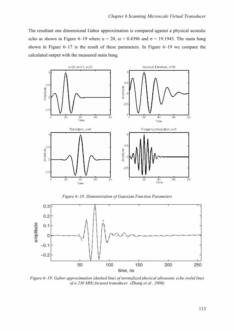
Chapter 6 Scanning Microscale Virtual Transducer
113
The resultant one dimensional Gabor approximation is compared against a physical acoustic
echo as shown in Figure 6–19 where u = 20, ω = 0.4396 and σ = 19.1943. The main bang
shown in Figure 6–17 is the result of these parameters. In Figure 6–19 we compare the
calculated output with the measured main bang.
Figure 6–18: Demonstration of Gaussian Function Parameters
Figure 6–19: Gabor approximation (dashed line) of normalized physical ultrasonic echo (solid line)
of a 230 MHz focused transducer. (Zhang et al., 2008)
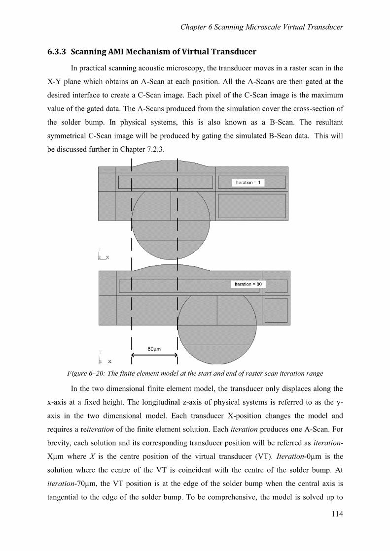
Chapter 6 Scanning Microscale Virtual Transducer
114
6.3.3 Scanning AMI Mechanism of Virtual Transducer
In practical scanning acoustic microscopy, the transducer moves in a raster scan in the
X-Y plane which obtains an A-Scan at each position. All the A-Scans are then gated at the
desired interface to create a C-Scan image. Each pixel of the C-Scan image is the maximum
value of the gated data. The A-Scans produced from the simulation cover the cross-section of
the solder bump. In physical systems, this is also known as a B-Scan. The resultant
symmetrical C-Scan image will be produced by gating the simulated B-Scan data. This will
be discussed further in Chapter 7.2.3.
Figure 6–20: The finite element model at the start and end of raster scan iteration range
In the two dimensional finite element model, the transducer only displaces along the
x-axis at a fixed height. The longitudinal z-axis of physical systems is referred to as the y-
axis in the two dimensional model. Each transducer X-position changes the model and
requires a reiteration of the finite element solution. Each iteration produces one A-Scan. For
brevity, each solution and its corresponding transducer position will be referred as iteration-
Xµm where X is the centre position of the virtual transducer (VT). Iteration-0µm is the
solution where the centre of the VT is coincident with the centre of the solder bump. At
iteration-70µm, the VT position is at the edge of the solder bump when the central axis is
tangential to the edge of the solder bump. To be comprehensive, the model is solved up to
Chapter 6 Scanning Microscale Virtual Transducer
115
iteration-80µm. Figure 6–20 shows the finite element model at the initial and final iteration
of the experiment. The scanning resolution for this experiment is set at 1µm. It can be
arbitrarily adjusted with a linear impact on computational cost. The models are solved with
(Figure 6–4) and without (Figure 6–20) the under bump metallization (UBM). The data is
organized into two sets with 80 iterations each.

Chapter 7 Novel Post Processing Algorithms
116
Chapter 7
Novel Post Processing
Algorithms
Chapter 7 Novel Post Processing Algorithms
117
7 Novel Post Processing Algorithms
The C-scan provides a plane-type view of the location and size of test specimen
features. The plane of the image is parallel to the scan pattern of the transducer. In physical
systems, C-scan images are produced with an automated data acquisition system, such as a
computer controlled immersion scanning system. Typically, a data collection gate is
established on the A-scan and the amplitude or the time-of-flight of the signal is recorded at
regular intervals as the transducer is scanned over the test piece. The relative signal amplitude
or the time-of-flight is displayed as a shade of gray or a colour for each of the positions where
data was recorded. The C-scan provides an image of the features that reflect and scatter the
sound within and on the surfaces of the test piece.
This chapter will talk about two post processing algorithms invented to interpret the
data obtained from the finite element solution. To proceed, it is important to understand the
source of data which has not yet been presented at this point. The simulation produced two
sets of data. One pertains to the acoustic response of reflections received by the virtual
transducer. This data set represents information obtained from physical AMI operations. The
second data set is the across section “slides” which measures the acoustic wave as it
propagates through the sample. Each slide is a specific time and the whole data is packaged
into a three dimensional array. To be clear, the first data set is a simulated B-Scan of the
sample. The second data set is a movie of the acoustic wave propagating through the sample.
On top of this, there are three primary model of the sample which are named Model A, B and
C respectively. The context of these different models will be apparently in during the
discussion sections. In the meantime, be informed that Model A is the typical solder bump
construction. Model B is constructed with the solder bump connected directly to the silicon
without an interconnecting Under Bump Metallization layer. Model C is similar to Model A
but with a crack introduced in the solder bump. Refer to Chapter 8.1for more details.
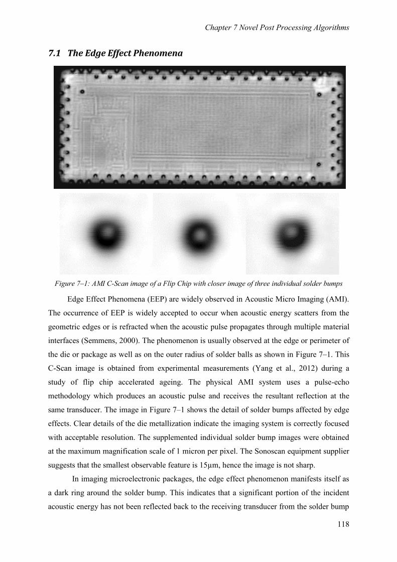
Chapter 7 Novel Post Processing Algorithms
118
7.1 The Edge Effect Phenomena
Figure 7–1: AMI C-Scan image of a Flip Chip with closer image of three individual solder bumps
Edge Effect Phenomena (EEP) are widely observed in Acoustic Micro Imaging (AMI).
The occurrence of EEP is widely accepted to occur when acoustic energy scatters from the
geometric edges or is refracted when the acoustic pulse propagates through multiple material
interfaces (Semmens, 2000). The phenomenon is usually observed at the edge or perimeter of
the die or package as well as on the outer radius of solder balls as shown in Figure 7–1. This
C-Scan image is obtained from experimental measurements (Yang et al., 2012) during a
study of flip chip accelerated ageing. The physical AMI system uses a pulse-echo
methodology which produces an acoustic pulse and receives the resultant reflection at the
same transducer. The image in Figure 7–1 shows the detail of solder bumps affected by edge
effects. Clear details of the die metallization indicate the imaging system is correctly focused
with acceptable resolution. The supplemented individual solder bump images were obtained
at the maximum magnification scale of 1 micron per pixel. The Sonoscan equipment supplier
suggests that the smallest observable feature is 15µm, hence the image is not sharp.
In imaging microelectronic packages, the edge effect phenomenon manifests itself as
a dark ring around the solder bump. This indicates that a significant portion of the incident
acoustic energy has not been reflected back to the receiving transducer from the solder bump
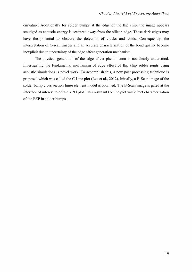
Chapter 7 Novel Post Processing Algorithms
119
curvature. Additionally for solder bumps at the edge of the flip chip, the image appears
smudged as acoustic energy is scattered away from the silicon edge. These dark edges may
have the potential to obscure the detection of cracks and voids. Consequently, the
interpretation of C-scan images and an accurate characterization of the bond quality become
inexplicit due to uncertainty of the edge effect generation mechanism.
The physical generation of the edge effect phenomenon is not clearly understood.
Investigating the fundamental mechanism of edge effect of flip chip solder joints using
acoustic simulations is novel work. To accomplish this, a new post processing technique is
proposed which was called the C-Line plot (Lee et al., 2012). Initially, a B-Scan image of the
solder bump cross section finite element model is obtained. The B-Scan image is gated at the
interface of interest to obtain a 2D plot. This resultant C-Line plot will direct characterization
of the EEP in solder bumps.
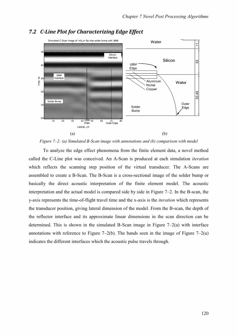
Chapter 7 Novel Post Processing Algorithms
120
7.2 C-Line Plot for Characterizing Edge Effect
(a) (b)
Figure 7–2: (a) Simulated B-Scan image with annotations and (b) comparison with model
To analyze the edge effect phenomena from the finite element data, a novel method
called the C-Line plot was conceived. An A-Scan is produced at each simulation iteration
which reflects the scanning step position of the virtual transducer. The A-Scans are
assembled to create a B-Scan. The B-Scan is a cross-sectional image of the solder bump or
basically the direct acoustic interpretation of the finite element model. The acoustic
interpretation and the actual model is compared side by side in Figure 7–2. In the B-scan, the
y-axis represents the time-of-flight travel time and the x-axis is the iteration which represents
the transducer position, giving lateral dimension of the model. From the B-scan, the depth of
the reflector interface and its approximate linear dimensions in the scan direction can be
determined. This is shown in the simulated B-Scan image in Figure 7–2(a) with interface
annotations with reference to Figure 7–2(b). The bands seen in the image of Figure 7–2(a)
indicates the different interfaces which the acoustic pulse travels through.
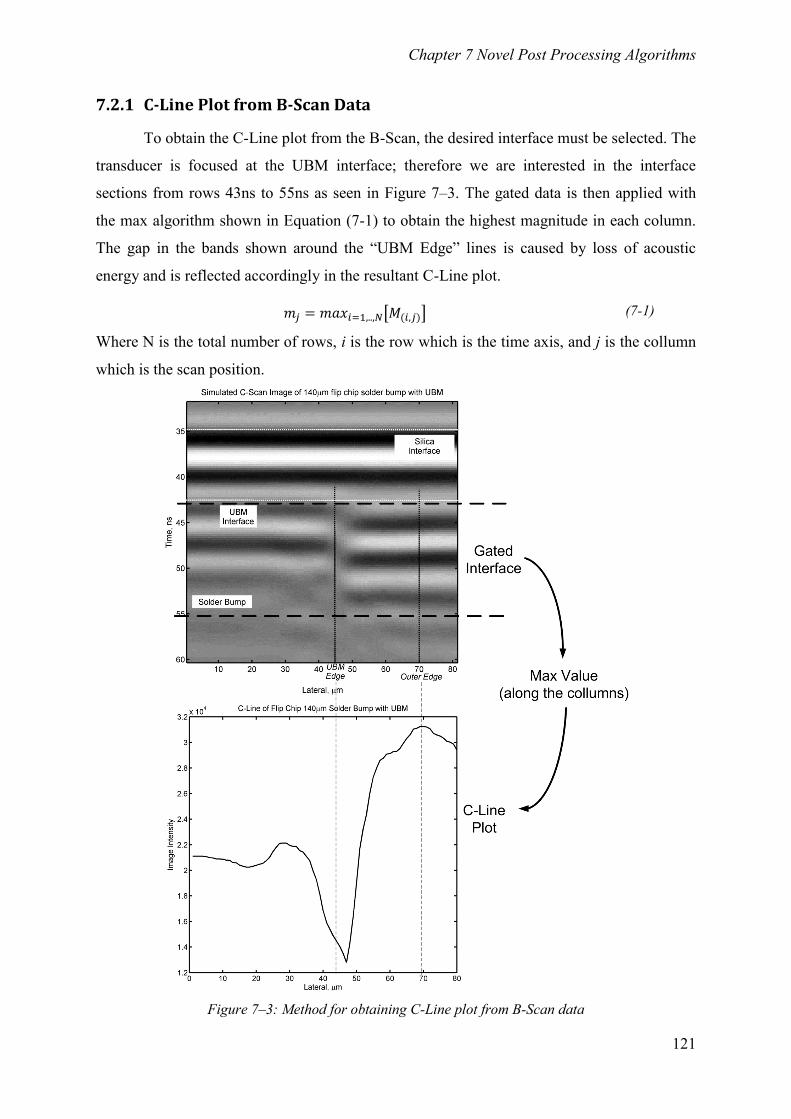
Chapter 7 Novel Post Processing Algorithms
121
7.2.1 C-Line Plot from B-Scan Data
To obtain the C-Line plot from the B-Scan, the desired interface must be selected. The
transducer is focused at the UBM interface; therefore we are interested in the interface
sections from rows 43ns to 55ns as seen in Figure 7–3. The gated data is then applied with
the max algorithm shown in Equation (7-1) to obtain the highest magnitude in each column.
The gap in the bands shown around the “UBM Edge” lines is caused by loss of acoustic
energy and is reflected accordingly in the resultant C-Line plot.
Where N is the total number of rows, i is the row which is the time axis, and j is the collumn
which is the scan position.
Figure 7–3: Method for obtaining C-Line plot from B-Scan data
(7-1)
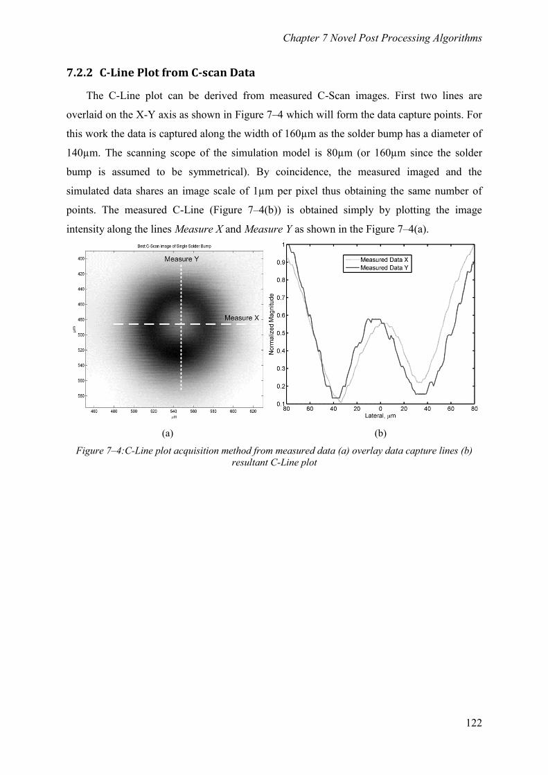
Chapter 7 Novel Post Processing Algorithms
122
7.2.2 C-Line Plot from C-scan Data
The C-Line plot can be derived from measured C-Scan images. First two lines are
overlaid on the X-Y axis as shown in Figure 7–4 which will form the data capture points. For
this work the data is captured along the width of 160µm as the solder bump has a diameter of
140µm. The scanning scope of the simulation model is 80µm (or 160µm since the solder
bump is assumed to be symmetrical). By coincidence, the measured imaged and the
simulated data shares an image scale of 1µm per pixel thus obtaining the same number of
points. The measured C-Line (Figure 7–4(b)) is obtained simply by plotting the image
intensity along the lines Measure X and Measure Y as shown in the Figure 7–4(a).
(a) (b)
Figure 7–4:C-Line plot acquisition method from measured data (a) overlay data capture lines (b)
resultant C-Line plot
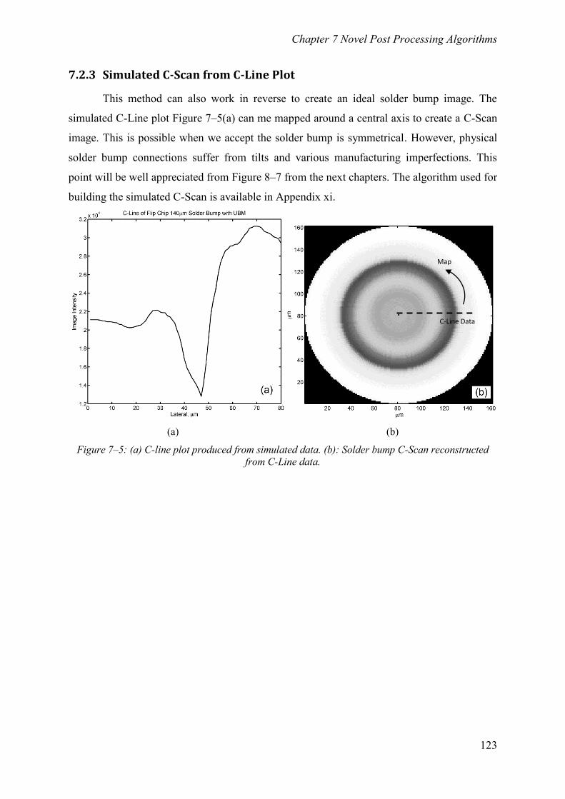
Chapter 7 Novel Post Processing Algorithms
123
7.2.3 Simulated C-Scan from C-Line Plot
This method can also work in reverse to create an ideal solder bump image. The
simulated C-Line plot Figure 7–5(a) can me mapped around a central axis to create a C-Scan
image. This is possible when we accept the solder bump is symmetrical. However, physical
solder bump connections suffer from tilts and various manufacturing imperfections. This
point will be well appreciated from Figure 8–7 from the next chapters. The algorithm used for
building the simulated C-Scan is available in Appendix xi.
(a) (b)
Figure 7–5: (a) C-line plot produced from simulated data. (b): Solder bump C-Scan reconstructed
from C-Line data.
C-Line Data
Map
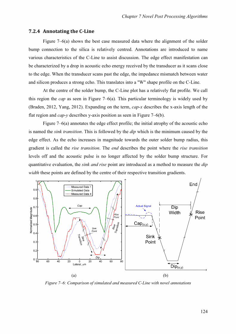
Chapter 7 Novel Post Processing Algorithms
124
7.2.4 Annotating the C-Line
Figure 7–6(a) shows the best case measured data where the alignment of the solder
bump connection to the silica is relatively centred. Annotations are introduced to name
various characteristics of the C-Line to assist discussion. The edge effect manifestation can
be characterized by a drop in acoustic echo energy received by the transducer as it scans close
to the edge. When the transducer scans past the edge, the impedance mismatch between water
and silicon produces a strong echo. This translates into a "W" shape profile on the C-Line.
At the centre of the solder bump, the C-Line plot has a relatively flat profile. We call
this region the cap as seen in Figure 7–6(a). This particular terminology is widely used by
(Braden, 2012, Yang, 2012). Expanding on the term, cap-x describes the x-axis length of the
flat region and cap-y describes y-axis position as seen in Figure 7–6(b).
Figure 7–6(a) annotates the edge effect profile; the initial atrophy of the acoustic echo
is named the sink transition. This is followed by the dip which is the minimum caused by the
edge effect. As the echo increases in magnitude towards the outer solder bump radius, this
gradient is called the rise transition. The end describes the point where the rise transition
levels off and the acoustic pulse is no longer affected by the solder bump structure. For
quantitative evaluation, the sink and rise point are introduced as a method to measure the dip
width these points are defined by the centre of their respective transition gradients.
(a) (b)
Figure 7–6: Comparison of simulated and measured C-Line with novel annotations
Chapter 7 Novel Post Processing Algorithms
125
7.2.5 Discussion: C-Line Plot
The "gap" around 45µm (marked as UBM Edge) in the B-Scan (Figure 7–2) shows
the edge effect phenomenon. This is the region of interest which requires additional analysis.
The edge effect in the simulated data is less pronounced compared its measured counterpart.
This is expected due to the silicon die model being thinner than physical samples. Die back
thinning is a technique used to reduce the presence of edge effects in AMI images (Semmens
and Kessler, 1998). This technique damages the sample by removing inert layers from the
sample, so would not be considered a non-destructive method. Aside from a smaller edge
effect, the plot shows considerably more detail then the measured C-Line. The AMI
equipment used to obtain the measured samples is expected to define features as small as
15µm. Used at the scale of 1µm per pixel; the images were obtained outside the operational
limits of the equipment. The resultant image appears to be out of focus. More importantly,
fine details like those seen in Figure 7–5(a) are expected to be lost.
This technique allows C-Scan images of solder bumps to be simplified and quantified.
This is particularly useful when dealing with solder bump images that has an off centre cap.
Works like (Yang, 2012) show that designing an algorithm that detects the centre of the
solder bump from a C-Scan is a complex endeavour. Since it is established that the rise
transition is constant, the C-Line method offers another form of calibration. In addition,
multiple C-Lines extracted from C-Scan images can be averaged and/or extrapolated to
assume perfect alignment as shown in Figure 7–5(b). This allows the effects of sample tilting
to be ignored and the analysis to be concentrated on the quality of the bonds.
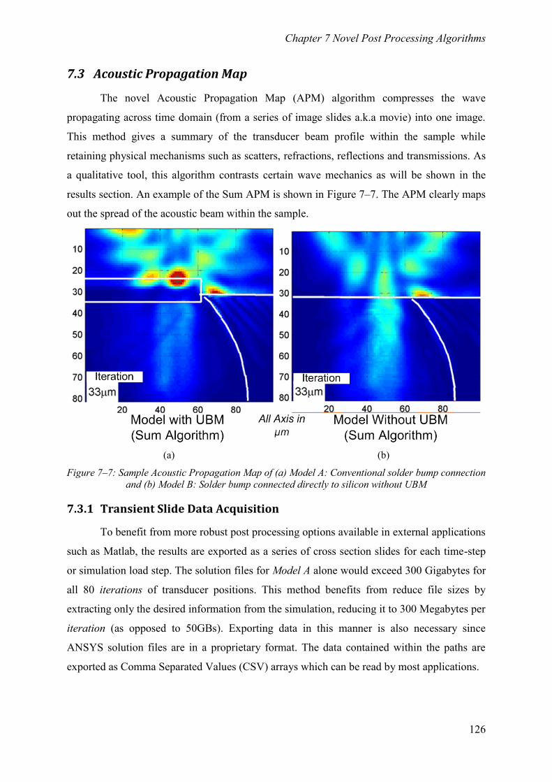
Chapter 7 Novel Post Processing Algorithms
126
7.3 Acoustic Propagation Map
The novel Acoustic Propagation Map (APM) algorithm compresses the wave
propagating across time domain (from a series of image slides a.k.a movie) into one image.
This method gives a summary of the transducer beam profile within the sample while
retaining physical mechanisms such as scatters, refractions, reflections and transmissions. As
a qualitative tool, this algorithm contrasts certain wave mechanics as will be shown in the
results section. An example of the Sum APM is shown in Figure 7–7. The APM clearly maps
out the spread of the acoustic beam within the sample.
(a) (b)
Figure 7–7: Sample Acoustic Propagation Map of (a) Model A: Conventional solder bump connection
and (b) Model B: Solder bump connected directly to silicon without UBM
7.3.1 Transient Slide Data Acquisition
To benefit from more robust post processing options available in external applications
such as Matlab, the results are exported as a series of cross section slides for each time-step
or simulation load step. The solution files for Model A alone would exceed 300 Gigabytes for
all 80 iterations of transducer positions. This method benefits from reduce file sizes by
extracting only the desired information from the simulation, reducing it to 300 Megabytes per
iteration (as opposed to 50GBs). Exporting data in this manner is also necessary since
ANSYS solution files are in a proprietary format. The data contained within the paths are
exported as Comma Separated Values (CSV) arrays which can be read by most applications.
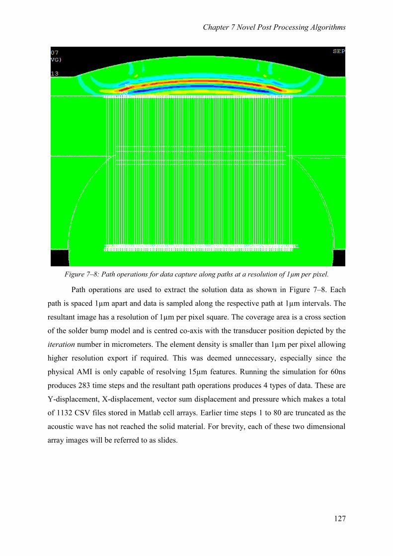
Chapter 7 Novel Post Processing Algorithms
127
Figure 7–8: Path operations for data capture along paths at a resolution of 1µm per pixel.
Path operations are used to extract the solution data as shown in Figure 7–8. Each
path is spaced 1µm apart and data is sampled along the respective path at 1µm intervals. The
resultant image has a resolution of 1µm per pixel square. The coverage area is a cross section
of the solder bump model and is centred co-axis with the transducer position depicted by the
iteration number in micrometers. The element density is smaller than 1µm per pixel allowing
higher resolution export if required. This was deemed unnecessary, especially since the
physical AMI is only capable of resolving 15µm features. Running the simulation for 60ns
produces 283 time steps and the resultant path operations produces 4 types of data. These are
Y-displacement, X-displacement, vector sum displacement and pressure which makes a total
of 1132 CSV files stored in Matlab cell arrays. Earlier time steps 1 to 80 are truncated as the
acoustic wave has not reached the solid material. For brevity, each of these two dimensional
array images will be referred to as slides.
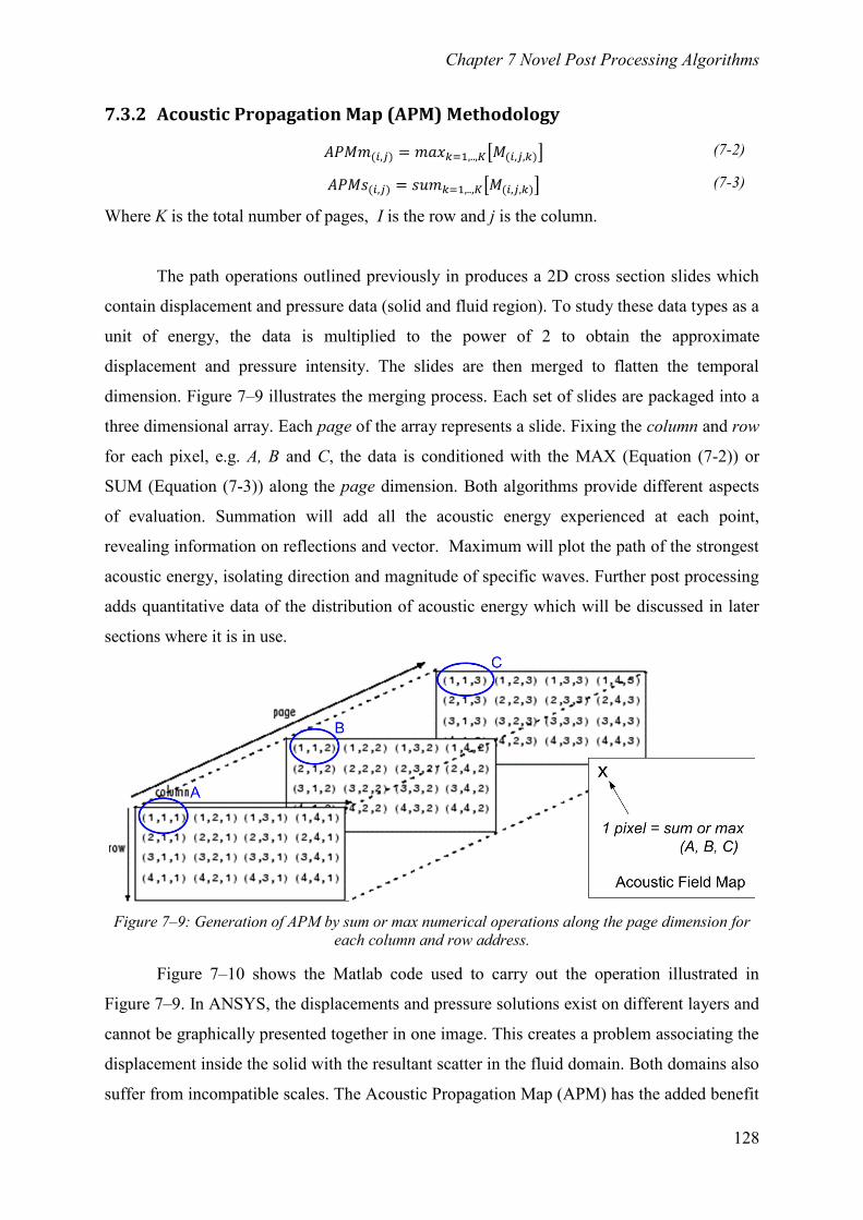
Chapter 7 Novel Post Processing Algorithms
128
7.3.2 Acoustic Propagation Map (APM) Methodology
(7-2)
(7-3)
Where K is the total number of pages, I is the row and j is the column.
The path operations outlined previously in produces a 2D cross section slides which
contain displacement and pressure data (solid and fluid region). To study these data types as a
unit of energy, the data is multiplied to the power of 2 to obtain the approximate
displacement and pressure intensity. The slides are then merged to flatten the temporal
dimension. Figure 7–9 illustrates the merging process. Each set of slides are packaged into a
three dimensional array. Each page of the array represents a slide. Fixing the column and row
for each pixel, e.g. A, B and C, the data is conditioned with the MAX (Equation (7-2)) or
SUM (Equation (7-3)) along the page dimension. Both algorithms provide different aspects
of evaluation. Summation will add all the acoustic energy experienced at each point,
revealing information on reflections and vector. Maximum will plot the path of the strongest
acoustic energy, isolating direction and magnitude of specific waves. Further post processing
adds quantitative data of the distribution of acoustic energy which will be discussed in later
sections where it is in use.
Figure 7–9: Generation of APM by sum or max numerical operations along the page dimension for
each column and row address.
Figure 7–10 shows the Matlab code used to carry out the operation illustrated in
Figure 7–9. In ANSYS, the displacements and pressure solutions exist on different layers and
cannot be graphically presented together in one image. This creates a problem associating the
displacement inside the solid with the resultant scatter in the fluid domain. Both domains also
suffer from incompatible scales. The Acoustic Propagation Map (APM) has the added benefit
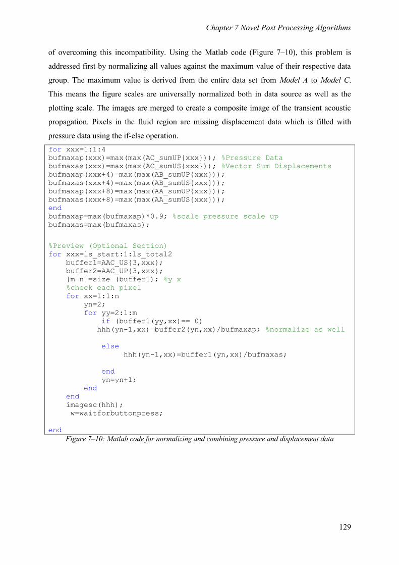
Chapter 7 Novel Post Processing Algorithms
129
of overcoming this incompatibility. Using the Matlab code (Figure 7–10), this problem is
addressed first by normalizing all values against the maximum value of their respective data
group. The maximum value is derived from the entire data set from Model A to Model C.
This means the figure scales are universally normalized both in data source as well as the
plotting scale. The images are merged to create a composite image of the transient acoustic
propagation. Pixels in the fluid region are missing displacement data which is filled with
pressure data using the if-else operation.
for xxx=1:1:4
bufmaxap(xxx)=max(max(AC_sumUP{xxx})); %Pressure Data
bufmaxas(xxx)=max(max(AC_sumUS{xxx})); %Vector Sum Displacements
bufmaxap(xxx+4)=max(max(AB_sumUP{xxx}));
bufmaxas(xxx+4)=max(max(AB_sumUS{xxx}));
bufmaxap(xxx+8)=max(max(AA_sumUP{xxx}));
bufmaxas(xxx+8)=max(max(AA_sumUS{xxx}));
end
bufmaxap=max(bufmaxap)*0.9; %scale pressure scale up
bufmaxas=max(bufmaxas);
%Preview (Optional Section)
for xxx=ls_start:1:ls_total2
buffer1=AAC_US{3,xxx};
buffer2=AAC_UP{3,xxx};
[m n]=size (buffer1); %y x
%check each pixel
for xx=1:1:n
yn=2;
for yy=2:1:m
if (buffer1(yy,xx)== 0)
hhh(yn-1,xx)=buffer2(yn,xx)/bufmaxap; %normalize as well
else
hhh(yn-1,xx)=buffer1(yn,xx)/bufmaxas;
end
yn=yn+1;
end
end
imagesc(hhh);
w=waitforbuttonpress;
end
Figure 7–10: Matlab code for normalizing and combining pressure and displacement data
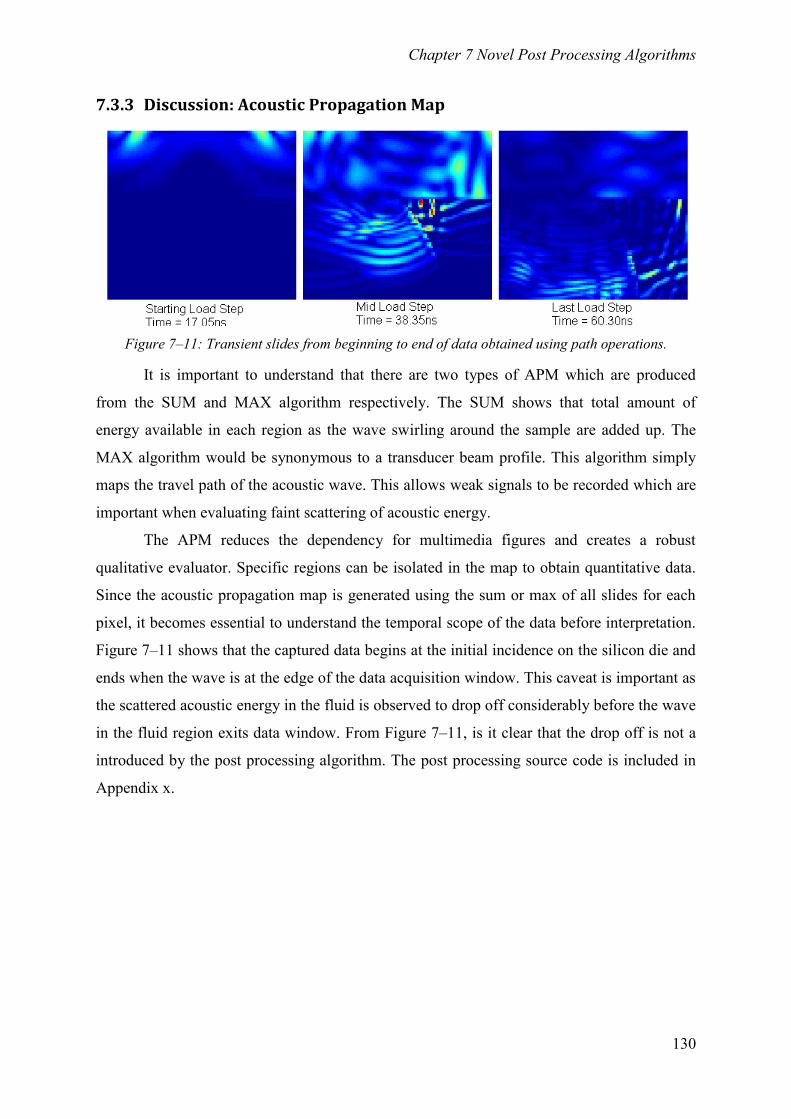
Chapter 7 Novel Post Processing Algorithms
130
7.3.3 Discussion: Acoustic Propagation Map
Figure 7–11: Transient slides from beginning to end of data obtained using path operations.
It is important to understand that there are two types of APM which are produced
from the SUM and MAX algorithm respectively. The SUM shows that total amount of
energy available in each region as the wave swirling around the sample are added up. The
MAX algorithm would be synonymous to a transducer beam profile. This algorithm simply
maps the travel path of the acoustic wave. This allows weak signals to be recorded which are
important when evaluating faint scattering of acoustic energy.
The APM reduces the dependency for multimedia figures and creates a robust
qualitative evaluator. Specific regions can be isolated in the map to obtain quantitative data.
Since the acoustic propagation map is generated using the sum or max of all slides for each
pixel, it becomes essential to understand the temporal scope of the data before interpretation.
Figure 7–11 shows that the captured data begins at the initial incidence on the silicon die and
ends when the wave is at the edge of the data acquisition window. This caveat is important as
the scattered acoustic energy in the fluid is observed to drop off considerably before the wave
in the fluid region exits data window. From Figure 7–11, is it clear that the drop off is not a
introduced by the post processing algorithm. The post processing source code is included in
Appendix x.

Chapter 8 Characterization of Acoustic Phenomena
131
Chapter 8
Characterization of Acoustic
Phenomena
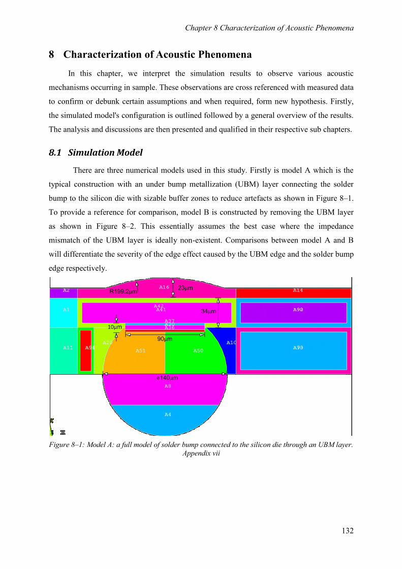
Chapter 8 Characterization of Acoustic Phenomena
132
8 Characterization of Acoustic Phenomena
In this chapter, we interpret the simulation results to observe various acoustic
mechanisms occurring in sample. These observations are cross referenced with measured data
to confirm or debunk certain assumptions and when required, form new hypothesis. Firstly,
the simulated model's configuration is outlined followed by a general overview of the results.
The analysis and discussions are then presented and qualified in their respective sub chapters.
8.1 Simulation Model
There are three numerical models used in this study. Firstly is model A which is the
typical construction with an under bump metallization (UBM) layer connecting the solder
bump to the silicon die with sizable buffer zones to reduce artefacts as shown in Figure 8–1.
To provide a reference for comparison, model B is constructed by removing the UBM layer
as shown in Figure 8–2. This essentially assumes the best case where the impedance
mismatch of the UBM layer is ideally non-existent. Comparisons between model A and B
will differentiate the severity of the edge effect caused by the UBM edge and the solder bump
edge respectively.
Figure 8–1: Model A: a full model of solder bump connected to the silicon die through an UBM layer.
Appendix vii
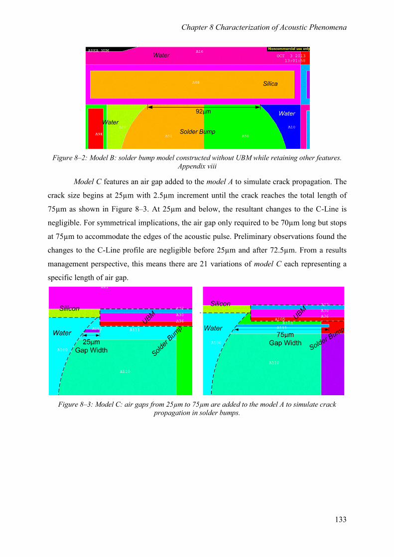
Chapter 8 Characterization of Acoustic Phenomena
133
Figure 8–2: Model B: solder bump model constructed without UBM while retaining other features.
Appendix viii
Model C features an air gap added to the model A to simulate crack propagation. The
crack size begins at 25µm with 2.5µm increment until the crack reaches the total length of
75µm as shown in Figure 8–3. At 25µm and below, the resultant changes to the C-Line is
negligible. For symmetrical implications, the air gap only required to be 70µm long but stops
at 75µm to accommodate the edges of the acoustic pulse. Preliminary observations found the
changes to the C-Line profile are negligible before 25µm and after 72.5µm. From a results
management perspective, this means there are 21 variations of model C each representing a
specific length of air gap.
Figure 8–3: Model C: air gaps from 25µm to 75µm are added to the model A to simulate crack
propagation in solder bumps.
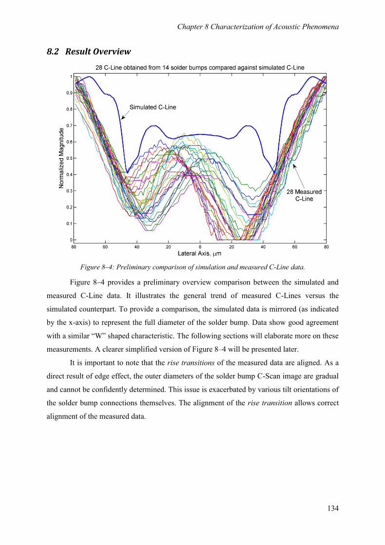
Chapter 8 Characterization of Acoustic Phenomena
134
8.2 Result Overview
Figure 8–4: Preliminary comparison of simulation and measured C-Line data.
Figure 8–4 provides a preliminary overview comparison between the simulated and
measured C-Line data. It illustrates the general trend of measured C-Lines versus the
simulated counterpart. To provide a comparison, the simulated data is mirrored (as indicated
by the x-axis) to represent the full diameter of the solder bump. Data show good agreement
with a similar “W” shaped characteristic. The following sections will elaborate more on these
measurements. A clearer simplified version of Figure 8–4 will be presented later.
It is important to note that the rise transitions of the measured data are aligned. As a
direct result of edge effect, the outer diameters of the solder bump C-Scan image are gradual
and cannot be confidently determined. This issue is exacerbated by various tilt orientations of
the solder bump connections themselves. The alignment of the rise transition allows correct
alignment of the measured data.
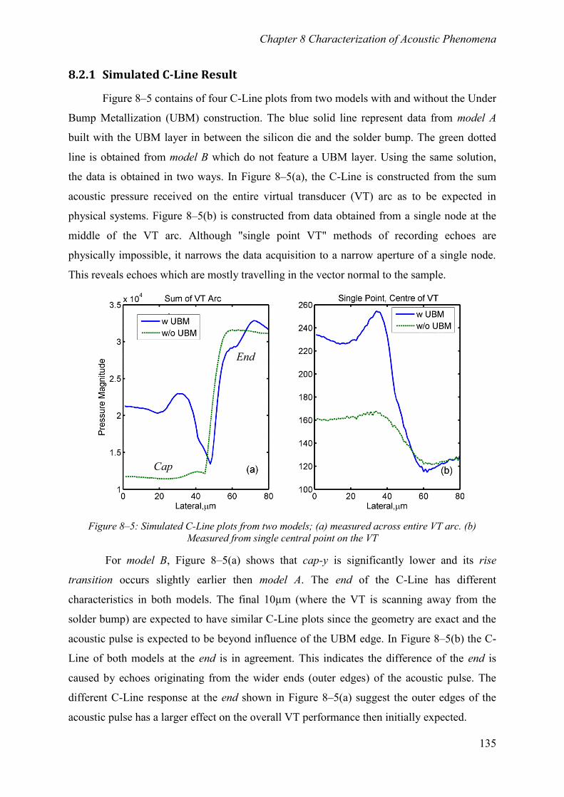
Chapter 8 Characterization of Acoustic Phenomena
135
8.2.1 Simulated C-Line Result
Figure 8–5 contains of four C-Line plots from two models with and without the Under
Bump Metallization (UBM) construction. The blue solid line represent data from model A
built with the UBM layer in between the silicon die and the solder bump. The green dotted
line is obtained from model B which do not feature a UBM layer. Using the same solution,
the data is obtained in two ways. In Figure 8–5(a), the C-Line is constructed from the sum
acoustic pressure received on the entire virtual transducer (VT) arc as to be expected in
physical systems. Figure 8–5(b) is constructed from data obtained from a single node at the
middle of the VT arc. Although "single point VT" methods of recording echoes are
physically impossible, it narrows the data acquisition to a narrow aperture of a single node.
This reveals echoes which are mostly travelling in the vector normal to the sample.
Figure 8–5: Simulated C-Line plots from two models; (a) measured across entire VT arc. (b)
Measured from single central point on the VT
For model B, Figure 8–5(a) shows that cap-y is significantly lower and its rise
transition occurs slightly earlier then model A. The end of the C-Line has different
characteristics in both models. The final 10µm (where the VT is scanning away from the
solder bump) are expected to have similar C-Line plots since the geometry are exact and the
acoustic pulse is expected to be beyond influence of the UBM edge. In Figure 8–5(b) the C-
Line of both models at the end is in agreement. This indicates the difference of the end is
caused by echoes originating from the wider ends (outer edges) of the acoustic pulse. The
different C-Line response at the end shown in Figure 8–5(a) suggest the outer edges of the
acoustic pulse has a larger effect on the overall VT performance then initially expected.
Cap
End
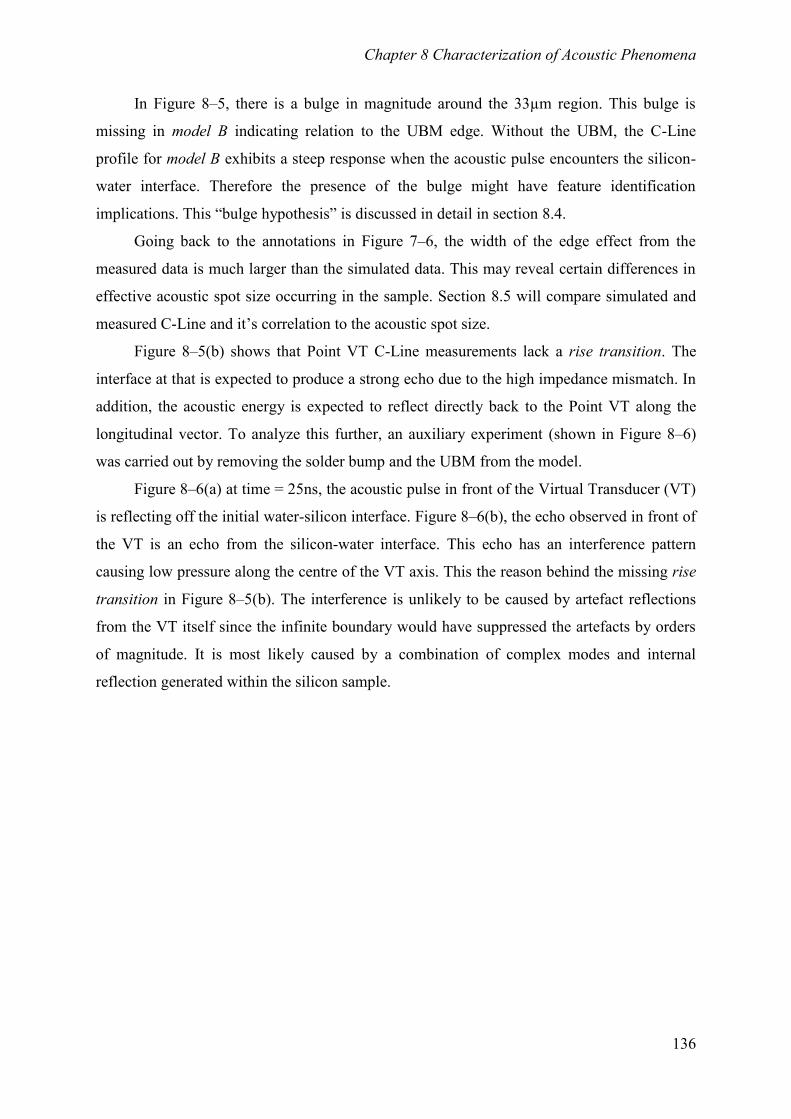
Chapter 8 Characterization of Acoustic Phenomena
136
In Figure 8–5, there is a bulge in magnitude around the 33µm region. This bulge is
missing in model B indicating relation to the UBM edge. Without the UBM, the C-Line
profile for model B exhibits a steep response when the acoustic pulse encounters the silicon-
water interface. Therefore the presence of the bulge might have feature identification
implications. This “bulge hypothesis” is discussed in detail in section 8.4.
Going back to the annotations in Figure 7–6, the width of the edge effect from the
measured data is much larger than the simulated data. This may reveal certain differences in
effective acoustic spot size occurring in the sample. Section 8.5 will compare simulated and
measured C-Line and it’s correlation to the acoustic spot size.
Figure 8–5(b) shows that Point VT C-Line measurements lack a rise transition. The
interface at that is expected to produce a strong echo due to the high impedance mismatch. In
addition, the acoustic energy is expected to reflect directly back to the Point VT along the
longitudinal vector. To analyze this further, an auxiliary experiment (shown in Figure 8–6)
was carried out by removing the solder bump and the UBM from the model.
Figure 8–6(a) at time = 25ns, the acoustic pulse in front of the Virtual Transducer (VT)
is reflecting off the initial water-silicon interface. Figure 8–6(b), the echo observed in front of
the VT is an echo from the silicon-water interface. This echo has an interference pattern
causing low pressure along the centre of the VT axis. This the reason behind the missing rise
transition in Figure 8–5(b). The interference is unlikely to be caused by artefact reflections
from the VT itself since the infinite boundary would have suppressed the artefacts by orders
of magnitude. It is most likely caused by a combination of complex modes and internal
reflection generated within the silicon sample.
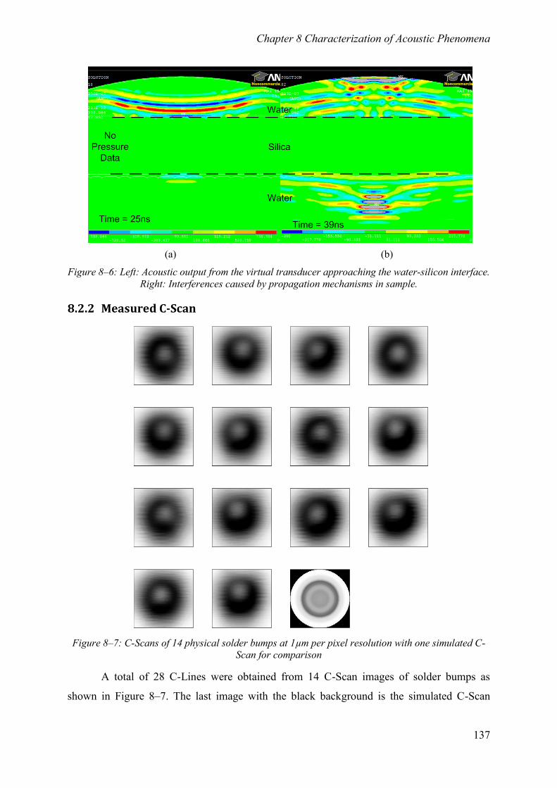
Chapter 8 Characterization of Acoustic Phenomena
137
(a) (b)
Figure 8–6: Left: Acoustic output from the virtual transducer approaching the water-silicon interface.
Right: Interferences caused by propagation mechanisms in sample.
8.2.2 Measured C-Scan
Figure 8–7: C-Scans of 14 physical solder bumps at 1µm per pixel resolution with one simulated C-
Scan for comparison
A total of 28 C-Lines were obtained from 14 C-Scan images of solder bumps as
shown in Figure 8–7. The last image with the black background is the simulated C-Scan
Chapter 8 Characterization of Acoustic Phenomena
138
inserted for reference. These images are extracted from solder bumps relatively far from the
edge of the silicon die. This is necessary as the edge of the silicon die causes an elongated
“smudge” like edge effect as seen in Figure 7–1. Each solder bump provides two C-Lines by
measuring the X and Y axis separately. The bright spot in the centre of the solder bump is
referred to as the "cap" as mentioned in chapter 7.2.4. At the cap, edge effects do not occur
and the interfaces through the sample are relatively transparent to the AMI. Surrounding the
cap is the edge effect which forms a dark ring indicating the lack of acoustic signal received
in that annular region. In most images, the cap is off centre. The exact reason for this is not
known but it is widely accepted to be caused by sample tilting. This off centre position of the
cap will affect the C-Line plot which needs to be taken into account during analysis. The C-
Line plot extracted from these images are shown in Figure 8–4 with the methodology
outlined in Figure 7–4.
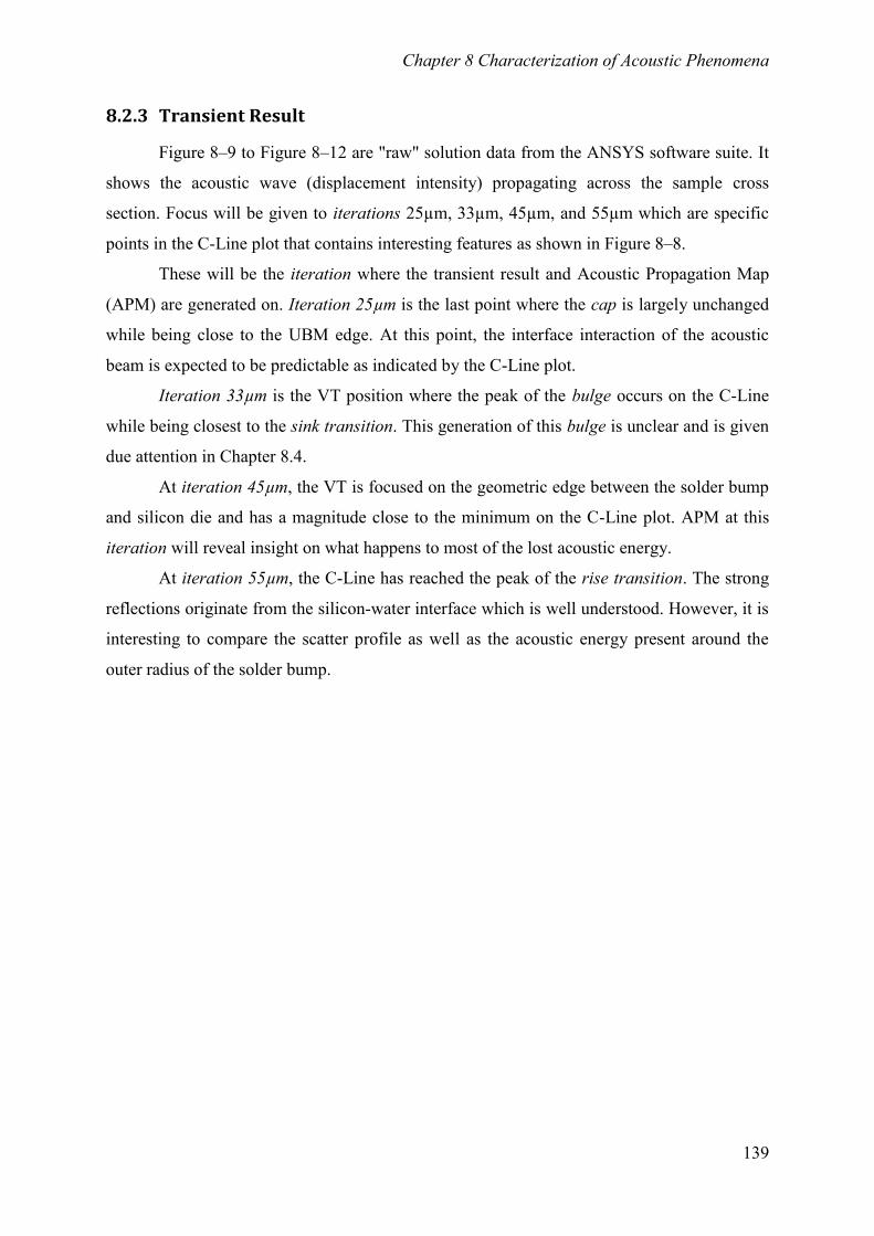
Chapter 8 Characterization of Acoustic Phenomena
139
8.2.3 Transient Result
Figure 8–9 to Figure 8–12 are "raw" solution data from the ANSYS software suite. It
shows the acoustic wave (displacement intensity) propagating across the sample cross
section. Focus will be given to iterations 25µm, 33µm, 45µm, and 55µm which are specific
points in the C-Line plot that contains interesting features as shown in Figure 8–8.
These will be the iteration where the transient result and Acoustic Propagation Map
(APM) are generated on. Iteration 25µm is the last point where the cap is largely unchanged
while being close to the UBM edge. At this point, the interface interaction of the acoustic
beam is expected to be predictable as indicated by the C-Line plot.
Iteration 33µm is the VT position where the peak of the bulge occurs on the C-Line
while being closest to the sink transition. This generation of this bulge is unclear and is given
due attention in Chapter 8.4.
At iteration 45µm, the VT is focused on the geometric edge between the solder bump
and silicon die and has a magnitude close to the minimum on the C-Line plot. APM at this
iteration will reveal insight on what happens to most of the lost acoustic energy.
At iteration 55µm, the C-Line has reached the peak of the rise transition. The strong
reflections originate from the silicon-water interface which is well understood. However, it is
interesting to compare the scatter profile as well as the acoustic energy present around the
outer radius of the solder bump.
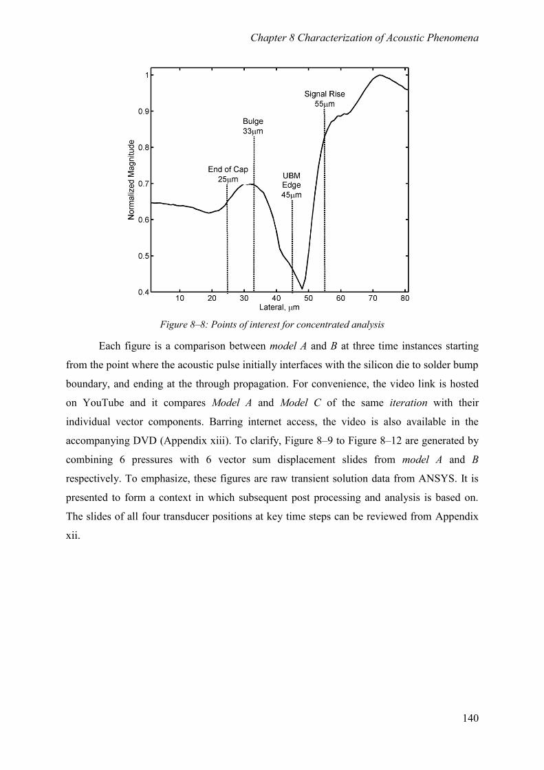
Chapter 8 Characterization of Acoustic Phenomena
140
Figure 8–8: Points of interest for concentrated analysis
Each figure is a comparison between model A and B at three time instances starting
from the point where the acoustic pulse initially interfaces with the silicon die to solder bump
boundary, and ending at the through propagation. For convenience, the video link is hosted
on YouTube and it compares Model A and Model C of the same iteration with their
individual vector components. Barring internet access, the video is also available in the
accompanying DVD (Appendix xiii). To clarify, Figure 8–9 to Figure 8–12 are generated by
combining 6 pressures with 6 vector sum displacement slides from model A and B
respectively. To emphasize, these figures are raw transient solution data from ANSYS. It is
presented to form a context in which subsequent post processing and analysis is based on.
The slides of all four transducer positions at key time steps can be reviewed from Appendix
xii.
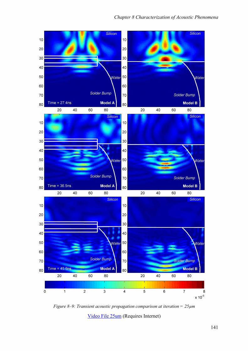
Chapter 8 Characterization of Acoustic Phenomena
141
Figure 8–9: Transient acoustic propagation comparison at iteration = 25µm
Video File 25um (Requires Internet)
Chapter 8 Characterization of Acoustic Phenomena
142
Figure 8–10: Transient acoustic propagation comparison at iteration = 33µm
Video File 33um (Requires Internet)
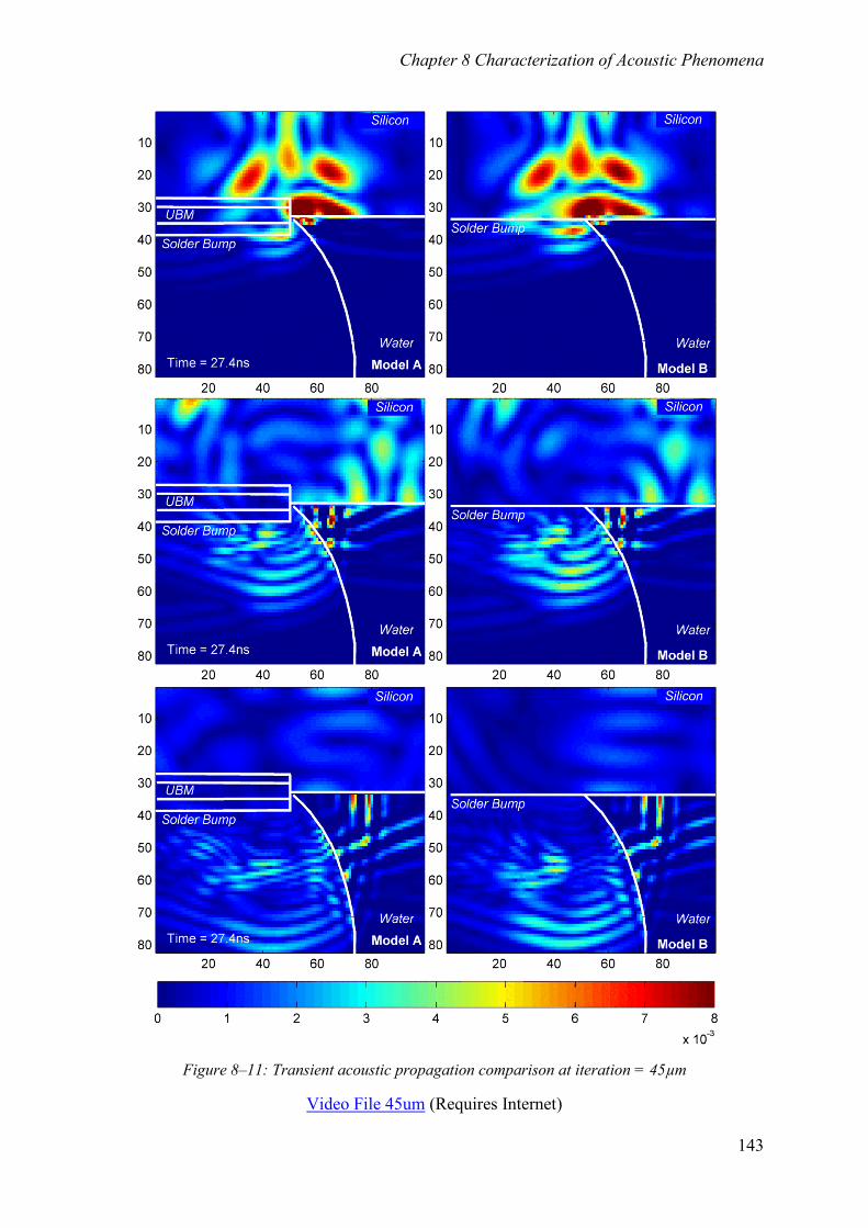
Chapter 8 Characterization of Acoustic Phenomena
143
Figure 8–11: Transient acoustic propagation comparison at iteration = 45µm
Video File 45um (Requires Internet)
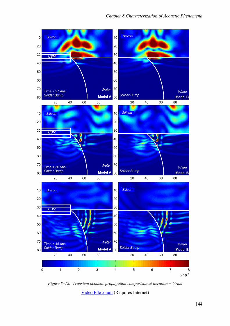
Chapter 8 Characterization of Acoustic Phenomena
144
Figure 8–12: Transient acoustic propagation comparison at iteration = 55µm
Video File 55um (Requires Internet)
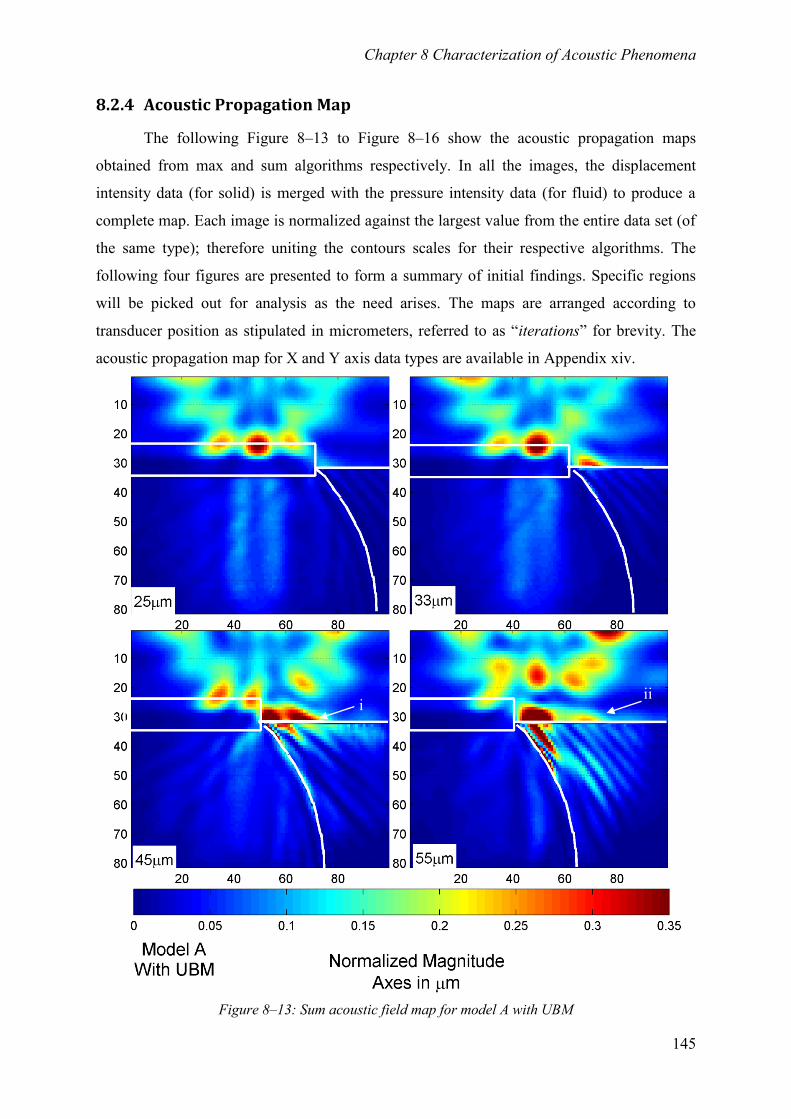
Chapter 8 Characterization of Acoustic Phenomena
145
8.2.4 Acoustic Propagation Map
The following Figure 8–13 to Figure 8–16 show the acoustic propagation maps
obtained from max and sum algorithms respectively. In all the images, the displacement
intensity data (for solid) is merged with the pressure intensity data (for fluid) to produce a
complete map. Each image is normalized against the largest value from the entire data set (of
the same type); therefore uniting the contours scales for their respective algorithms. The
following four figures are presented to form a summary of initial findings. Specific regions
will be picked out for analysis as the need arises. The maps are arranged according to
transducer position as stipulated in micrometers, referred to as “iterations” for brevity. The
acoustic propagation map for X and Y axis data types are available in Appendix xiv.
Figure 8–13: Sum acoustic field map for model A with UBM
i ii
Chapter 8 Characterization of Acoustic Phenomena
146
The APM in Figure 8–13 shows the scattered acoustic energy in the fluid region
increasing as the VT is positioned closer to the edge. This preliminary observation is in line
with the popular assumption that the edge effect is generated mainly from acoustic energy
diffused by the sample edges. This hypothesis will be referred to as the scatter theory and will
be discussed in greater detail in section 8.3.
Figure 8–13 and Figure 8–14 shows significant magnitude at the silicon to water
interface in iteration 45µm and 55µm at points (i) and (ii) indicated in the figures. This
indicates strong reflection as the incident and reflected waves are added together by the sum
algorithm. This clearly indicates a strong reflection due to the high impedance mismatch
between silicon and water. So far, we have just pointed out the obvious.
Firstly, consider that the contour profile of (i) and (ii) are observed identically in both
model A and model B of both Figure 8–13 and Figure 8–14. At 45µm, the edge effect occurs
while the C-Line has higher magnitudes at 55µm. This effect is most likely caused by
specific interactions with the UBM layer. Secondly, consider that at iterations 45µm and
55µm, the C-Line results defer between Model A and Model B. The dip occurs earlier with
Model B, although identical contours (i) and (ii) were observed in both figures. This
observation serves as a preliminary involvement of the UBM structure in the edge effect
generation. To test this, detailed measurements of the acoustic energy in the context of UBM
presence are required. The difference in penetrated acoustic energy with and without a UBM
present is outlined in Section 8.3.3.
From Figure 8–13 at iteration = 45µm, while the edge effect is apparent, a small
amount of acoustic energy is observed within the solder bump structure. Defect detection
may still be possible under these circumstances. However, at iteration 55µm the acoustic
propagation maps of both models A and B (Figure 8–13 and Figure 8–14) show minute
quantities of acoustic energy propagated into the solder bump. This will hinder any defect
detection mechanism from occurring. The presences of these energies are measured in
Chapter 8.3.3 and 8.3.4 respectively.
The next question then arises that strong reflections from the silicon-water interface
will overwhelm any signals reflected from defects in the solder bump. To study this, cracks
are applied to the solder bump and the simulation is rerun. The analysis of the C-Line profile
according to the width of gap type defects are discussed in section 8.6.
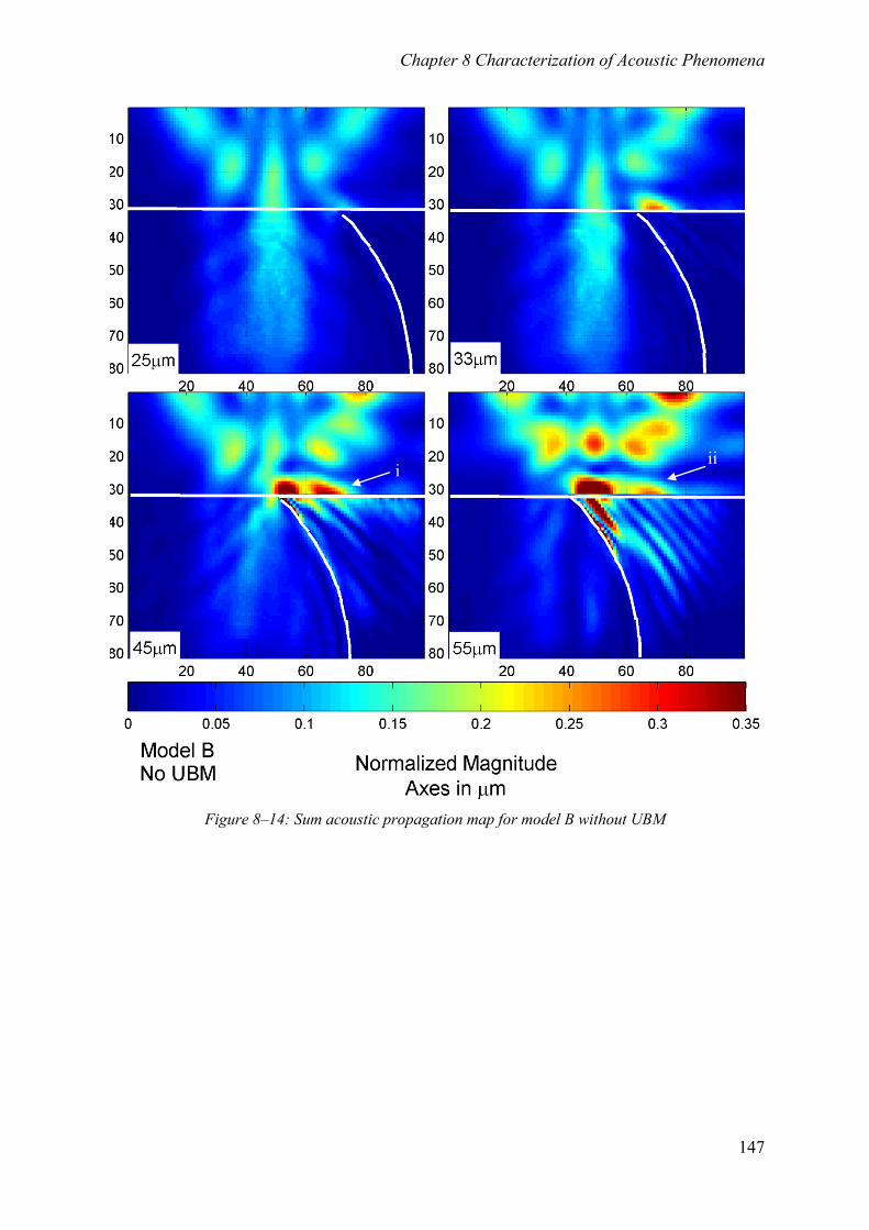
Chapter 8 Characterization of Acoustic Phenomena
147
Figure 8–14: Sum acoustic propagation map for model B without UBM
i ii
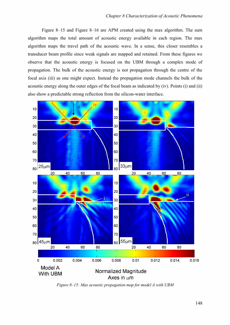
Chapter 8 Characterization of Acoustic Phenomena
148
Figure 8–15 and Figure 8–16 are APM created using the max algorithm. The sum
algorithm maps the total amount of acoustic energy available in each region. The max
algorithm maps the travel path of the acoustic wave. In a sense, this closer resembles a
transducer beam profile since weak signals are mapped and retained. From these figures we
observe that the acoustic energy is focused on the UBM through a complex mode of
propagation. The bulk of the acoustic energy is not propagation through the centre of the
focal axis (iii) as one might expect. Instead the propagation mode channels the bulk of the
acoustic energy along the outer edges of the focal beam as indicated by (iv). Points (i) and (ii)
also show a predictable strong reflection from the silicon-water interface.
Figure 8–15: Max acoustic propagation map for model A with UBM
iii iv
i ii
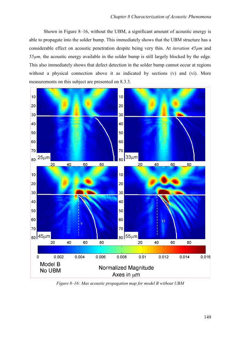
Chapter 8 Characterization of Acoustic Phenomena
149
Shown in Figure 8–16, without the UBM, a significant amount of acoustic energy is
able to propagate into the solder bump. This immediately shows that the UBM structure has a
considerable effect on acoustic penetration despite being very thin. At iteration 45µm and
55µm, the acoustic energy available in the solder bump is still largely blocked by the edge.
This also immediately shows that defect detection in the solder bump cannot occur at regions
without a physical connection above it as indicated by sections (v) and (vi). More
measurements on this subject are presented on 8.3.3.
Figure 8–16: Max acoustic propagation map for model B without UBM
v vi
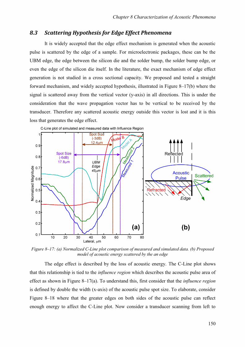
Chapter 8 Characterization of Acoustic Phenomena
150
8.3 Scattering Hypothesis for Edge Effect Phenomena
It is widely accepted that the edge effect mechanism is generated when the acoustic
pulse is scattered by the edge of a sample. For microelectronic packages, these can be the
UBM edge, the edge between the silicon die and the solder bump, the solder bump edge, or
even the edge of the silicon die itself. In the literature, the exact mechanism of edge effect
generation is not studied in a cross sectional capacity. We proposed and tested a straight
forward mechanism, and widely accepted hypothesis, illustrated in Figure 8–17(b) where the
signal is scattered away from the vertical vector (y-axis) in all directions. This is under the
consideration that the wave propagation vector has to be vertical to be received by the
transducer. Therefore any scattered acoustic energy outside this vector is lost and it is this
loss that generates the edge effect.
Figure 8–17: (a) Normalized C-Line plot comparison of measured and simulated data. (b) Proposed
model of acoustic energy scattered by the an edge
The edge effect is described by the loss of acoustic energy. The C-Line plot shows
that this relationship is tied to the influence region which describes the acoustic pulse area of
effect as shown in Figure 8–17(a). To understand this, first consider that the influence region
is defined by double the width (x-axis) of the acoustic pulse spot size. To elaborate, consider
Figure 8–18 where that the greater edges on both sides of the acoustic pulse can reflect
enough energy to affect the C-Line plot. Now consider a transducer scanning from left to
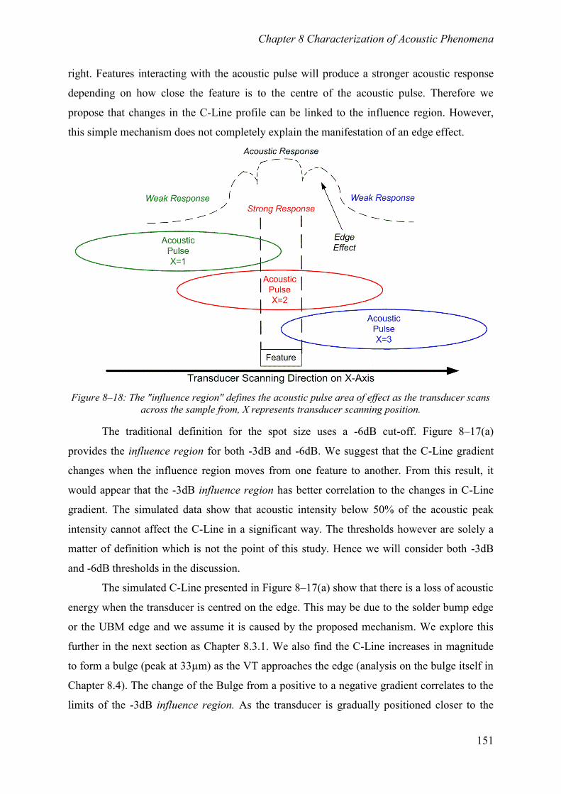
Chapter 8 Characterization of Acoustic Phenomena
151
right. Features interacting with the acoustic pulse will produce a stronger acoustic response
depending on how close the feature is to the centre of the acoustic pulse. Therefore we
propose that changes in the C-Line profile can be linked to the influence region. However,
this simple mechanism does not completely explain the manifestation of an edge effect.
Figure 8–18: The "influence region" defines the acoustic pulse area of effect as the transducer scans
across the sample from, X represents transducer scanning position.
The traditional definition for the spot size uses a -6dB cut-off. Figure 8–17(a)
provides the influence region for both -3dB and -6dB. We suggest that the C-Line gradient
changes when the influence region moves from one feature to another. From this result, it
would appear that the -3dB influence region has better correlation to the changes in C-Line
gradient. The simulated data show that acoustic intensity below 50% of the acoustic peak
intensity cannot affect the C-Line in a significant way. The thresholds however are solely a
matter of definition which is not the point of this study. Hence we will consider both -3dB
and -6dB thresholds in the discussion.
The simulated C-Line presented in Figure 8–17(a) show that there is a loss of acoustic
energy when the transducer is centred on the edge. This may be due to the solder bump edge
or the UBM edge and we assume it is caused by the proposed mechanism. We explore this
further in the next section as Chapter 8.3.1. We also find the C-Line increases in magnitude
to form a bulge (peak at 33µm) as the VT approaches the edge (analysis on the bulge itself in
Chapter 8.4). The change of the Bulge from a positive to a negative gradient correlates to the
limits of the -3dB influence region. As the transducer is gradually positioned closer to the
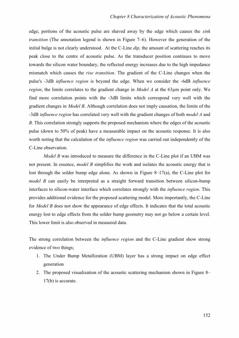
Chapter 8 Characterization of Acoustic Phenomena
152
edge, portions of the acoustic pulse are shaved away by the edge which causes the sink
transition (The annotation legend is shown in Figure 7–6). However the generation of the
initial bulge is not clearly understood. At the C-Line dip, the amount of scattering reaches its
peak close to the centre of acoustic pulse. As the transducer position continues to move
towards the silicon water boundary, the reflected energy increases due to the high impedance
mismatch which causes the rise transition. The gradient of the C-Line changes when the
pulse's -3dB influence region is beyond the edge. When we consider the -6dB influence
region, the limits correlates to the gradient change in Model A at the 63µm point only. We
find more correlation points with the -3dB limits which correspond very well with the
gradient changes in Model B. Although correlation does not imply causation, the limits of the
-3dB influence region has correlated very well with the gradient changes of both model A and
B. This correlation strongly supports the proposed mechanism where the edges of the acoustic
pulse (down to 50% of peak) have a measurable impact on the acoustic response. It is also
worth noting that the calculation of the influence region was carried out independently of the
C-Line observation.
Model B was introduced to measure the difference in the C-Line plot if an UBM was
not present. In essence, model B simplifies the work and isolates the acoustic energy that is
lost through the solder bump edge alone. As shown in Figure 8–17(a), the C-Line plot for
model B can easily be interpreted as a straight forward transition between silicon-bump
interfaces to silicon-water interface which correlates strongly with the influence region. This
provides additional evidence for the proposed scattering model. More importantly, the C-Line
for Model B does not show the appearance of edge effects. It indicates that the total acoustic
energy lost to edge effects from the solder bump geometry may not go below a certain level.
This lower limit is also observed in measured data.
The strong correlation between the influence region and the C-Line gradient show strong
evidence of two things;
1. The Under Bump Metallization (UBM) layer has a strong impact on edge effect
generation
2. The proposed visualization of the acoustic scattering mechanism shown in Figure 8–
17(b) is accurate.
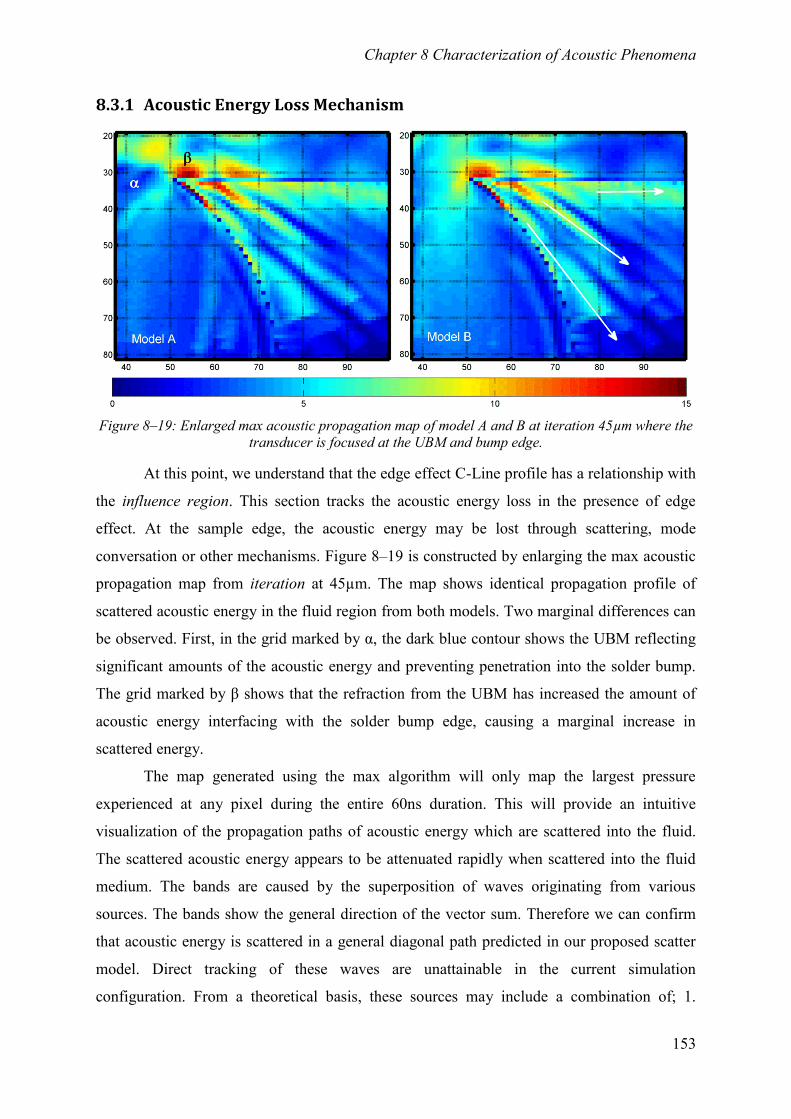
Chapter 8 Characterization of Acoustic Phenomena
153
8.3.1 Acoustic Energy Loss Mechanism
Figure 8–19: Enlarged max acoustic propagation map of model A and B at iteration 45µm where the
transducer is focused at the UBM and bump edge.
At this point, we understand that the edge effect C-Line profile has a relationship with
the influence region. This section tracks the acoustic energy loss in the presence of edge
effect. At the sample edge, the acoustic energy may be lost through scattering, mode
conversation or other mechanisms. Figure 8–19 is constructed by enlarging the max acoustic
propagation map from iteration at 45µm. The map shows identical propagation profile of
scattered acoustic energy in the fluid region from both models. Two marginal differences can
be observed. First, in the grid marked by α, the dark blue contour shows the UBM reflecting
significant amounts of the acoustic energy and preventing penetration into the solder bump.
The grid marked by β shows that the refraction from the UBM has increased the amount of
acoustic energy interfacing with the solder bump edge, causing a marginal increase in
scattered energy.
The map generated using the max algorithm will only map the largest pressure
experienced at any pixel during the entire 60ns duration. This will provide an intuitive
visualization of the propagation paths of acoustic energy which are scattered into the fluid.
The scattered acoustic energy appears to be attenuated rapidly when scattered into the fluid
medium. The bands are caused by the superposition of waves originating from various
sources. The bands show the general direction of the vector sum. Therefore we can confirm
that acoustic energy is scattered in a general diagonal path predicted in our proposed scatter
model. Direct tracking of these waves are unattainable in the current simulation
configuration. From a theoretical basis, these sources may include a combination of; 1.
Chapter 8 Characterization of Acoustic Phenomena
154
Refraction from the silicon plane and solder bump; 2. Scattering from the edge of the solder
bump; 3. Leakage from Lamb waves as the thickness of the silicon die is comparable
(Freedman, 1995) to the acoustic wavelength.
Both models in Figure 8–19 show a solid band along the silicon die marked by the
horizontal arrow. This unbroken trail on the acoustic map shows a considerable amount of
acoustic energy scattered in a horizontal vector (abbreviated as horizontal scatter). The lack
of interference pattern also indicates a solid pulse of energy travelling in that vector. This is
compared and confirmed with enlarged transient slides shown in Figure 8–20 (enlarged from
Figure 8–11). The data suggests that large portions of the scatter are refracted close to the
horizontal vector when the centre of acoustic pulse interfaces the model edge. This may
explain the loss of acoustic energy which generates the edge effect. The data also show that
the horizontal scatter is not affected by the presence of the UBM since it is present in both
model A and B and is caused primarily by the "silicon die-solder bump" edge.
Figure 8–20: Enlarged fluid region transient data of model A at iteration 45µm
The horizontal scatter is examined further by comparing the max acoustic propagation
map of iteration 45µm with that of 55µm. The contour scales exaggerated to enhance the
image. Figure 8–21 shows that at iteration 55µm ,there is no horizontal scatter as all the
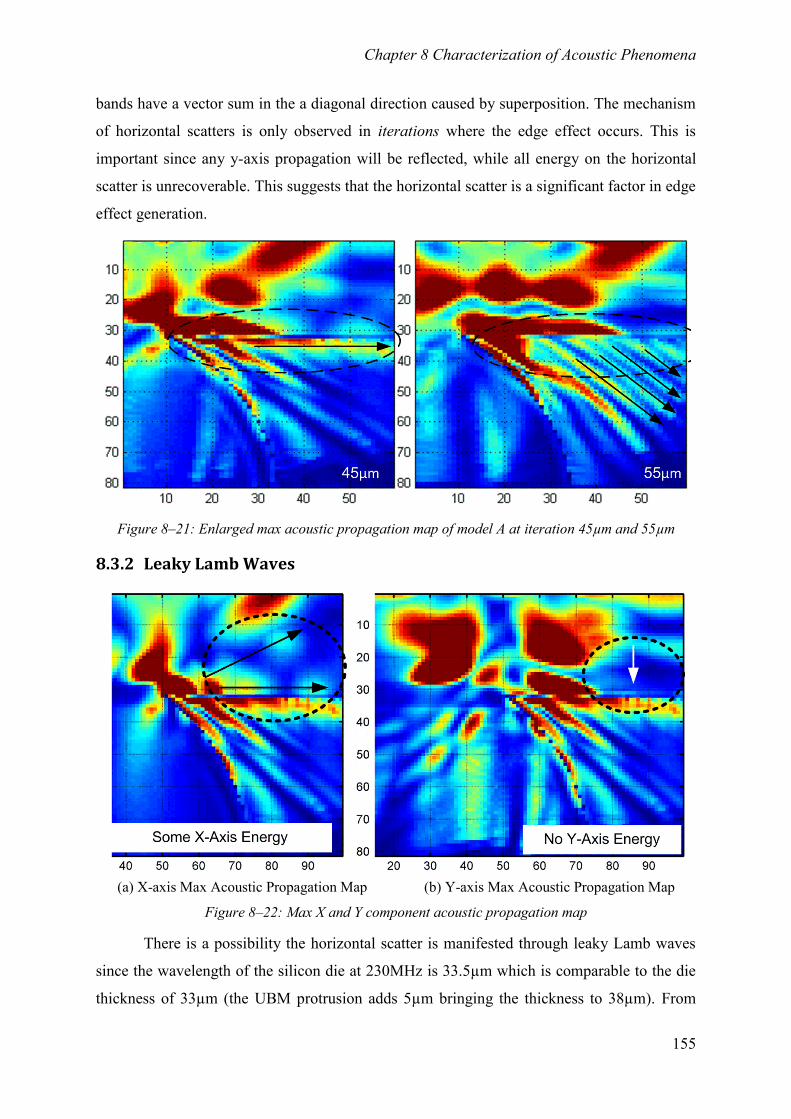
Chapter 8 Characterization of Acoustic Phenomena
155
bands have a vector sum in the a diagonal direction caused by superposition. The mechanism
of horizontal scatters is only observed in iterations where the edge effect occurs. This is
important since any y-axis propagation will be reflected, while all energy on the horizontal
scatter is unrecoverable. This suggests that the horizontal scatter is a significant factor in edge
effect generation.
Figure 8–21: Enlarged max acoustic propagation map of model A at iteration 45µm and 55µm
8.3.2 Leaky Lamb Waves
(a) X-axis Max Acoustic Propagation Map (b) Y-axis Max Acoustic Propagation Map
Figure 8–22: Max X and Y component acoustic propagation map
There is a possibility the horizontal scatter is manifested through leaky Lamb waves
since the wavelength of the silicon die at 230MHz is 33.5µm which is comparable to the die
thickness of 33µm (the UBM protrusion adds 5µm bringing the thickness to 38µm). From
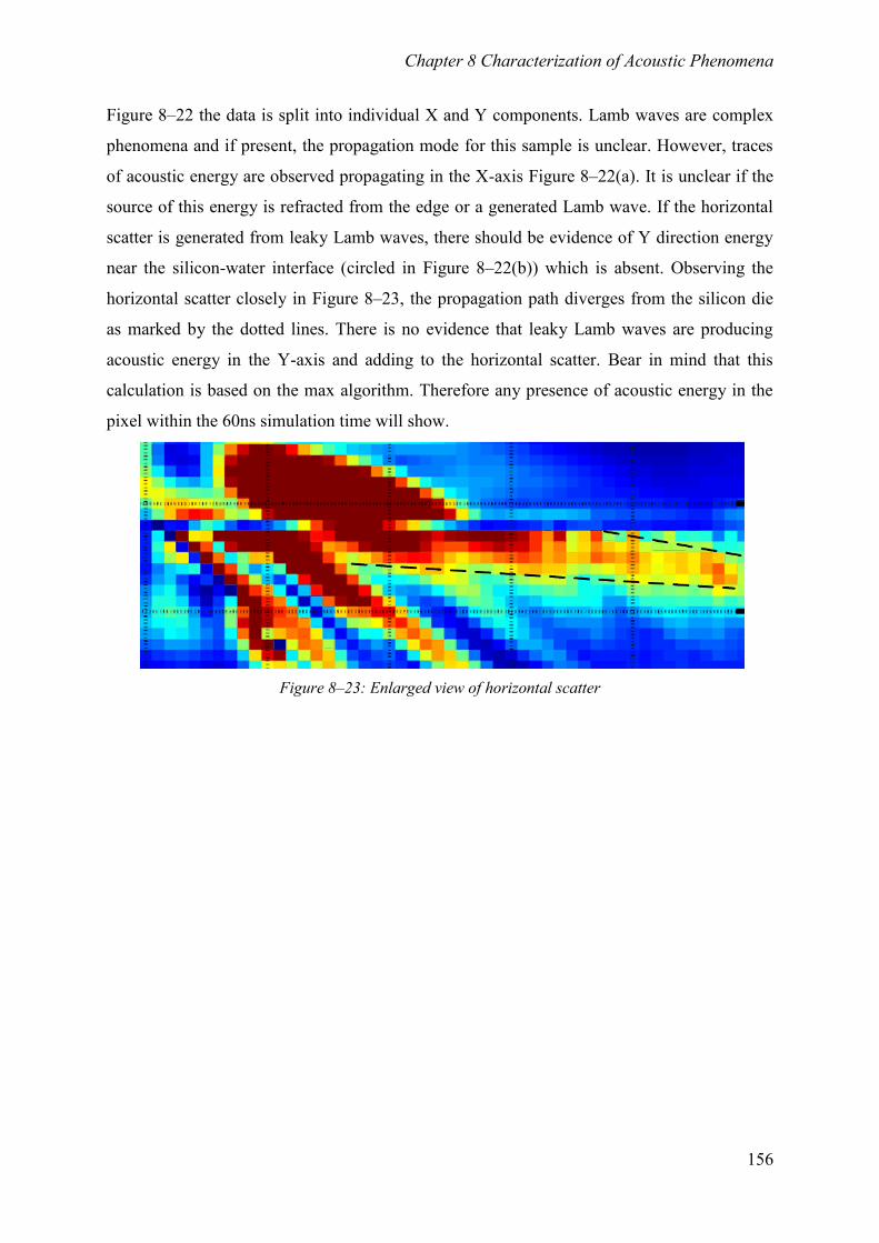
Chapter 8 Characterization of Acoustic Phenomena
156
Figure 8–22 the data is split into individual X and Y components. Lamb waves are complex
phenomena and if present, the propagation mode for this sample is unclear. However, traces
of acoustic energy are observed propagating in the X-axis Figure 8–22(a). It is unclear if the
source of this energy is refracted from the edge or a generated Lamb wave. If the horizontal
scatter is generated from leaky Lamb waves, there should be evidence of Y direction energy
near the silicon-water interface (circled in Figure 8–22(b)) which is absent. Observing the
horizontal scatter closely in Figure 8–23, the propagation path diverges from the silicon die
as marked by the dotted lines. There is no evidence that leaky Lamb waves are producing
acoustic energy in the Y-axis and adding to the horizontal scatter. Bear in mind that this
calculation is based on the max algorithm. Therefore any presence of acoustic energy in the
pixel within the 60ns simulation time will show.
Figure 8–23: Enlarged view of horizontal scatter
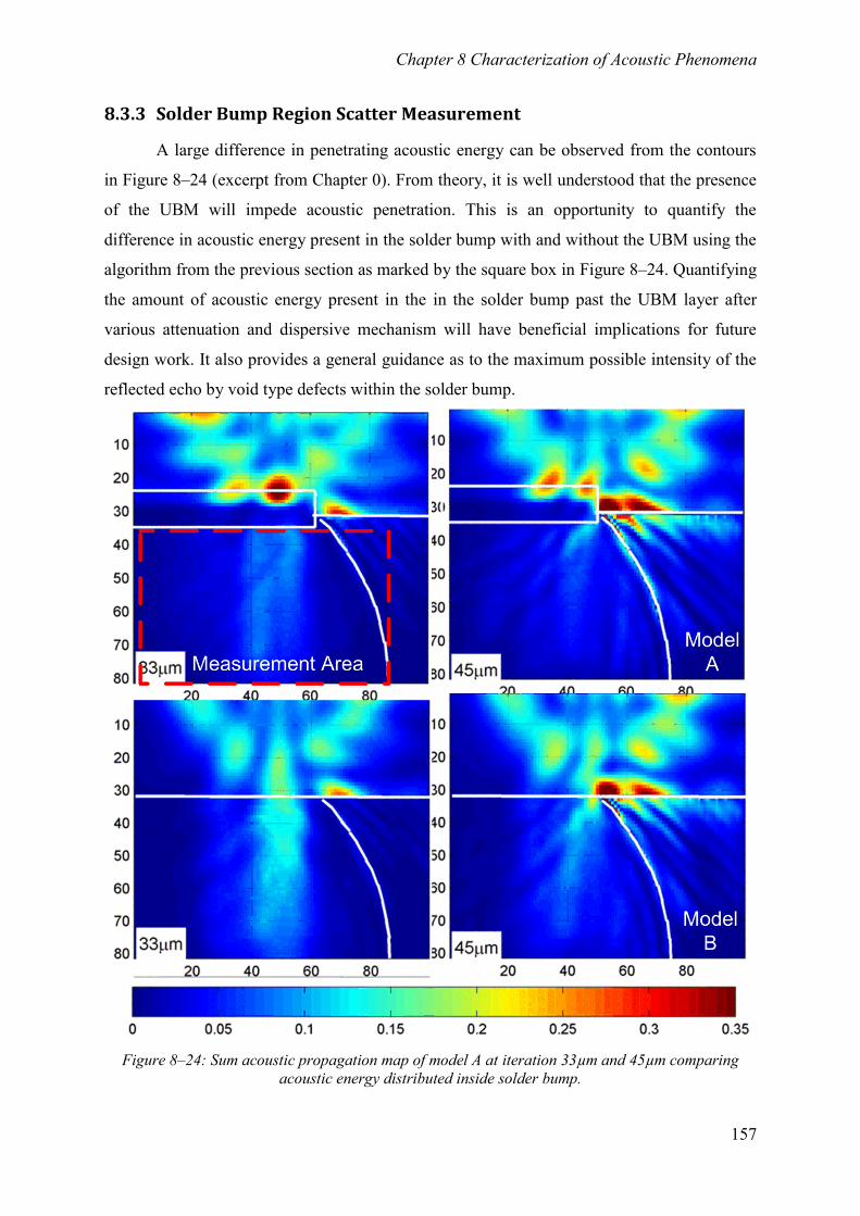
Chapter 8 Characterization of Acoustic Phenomena
157
8.3.3 Solder Bump Region Scatter Measurement
A large difference in penetrating acoustic energy can be observed from the contours
in Figure 8–24 (excerpt from Chapter 0). From theory, it is well understood that the presence
of the UBM will impede acoustic penetration. This is an opportunity to quantify the
difference in acoustic energy present in the solder bump with and without the UBM using the
algorithm from the previous section as marked by the square box in Figure 8–24. Quantifying
the amount of acoustic energy present in the in the solder bump past the UBM layer after
various attenuation and dispersive mechanism will have beneficial implications for future
design work. It also provides a general guidance as to the maximum possible intensity of the
reflected echo by void type defects within the solder bump.
Figure 8–24: Sum acoustic propagation map of model A at iteration 33µm and 45µm comparing
acoustic energy distributed inside solder bump.
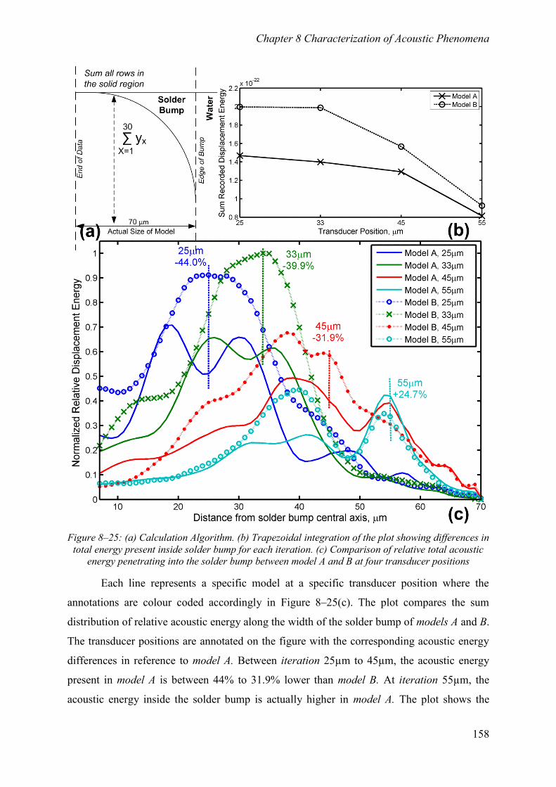
Chapter 8 Characterization of Acoustic Phenomena
158
Figure 8–25: (a) Calculation Algorithm. (b) Trapezoidal integration of the plot showing differences in
total energy present inside solder bump for each iteration. (c) Comparison of relative total acoustic
energy penetrating into the solder bump between model A and B at four transducer positions
Each line represents a specific model at a specific transducer position where the
annotations are colour coded accordingly in Figure 8–25(c). The plot compares the sum
distribution of relative acoustic energy along the width of the solder bump of models A and B.
The transducer positions are annotated on the figure with the corresponding acoustic energy
differences in reference to model A. Between iteration 25µm to 45µm, the acoustic energy
present in model A is between 44% to 31.9% lower than model B. At iteration 55µm, the
acoustic energy inside the solder bump is actually higher in model A. The plot shows the
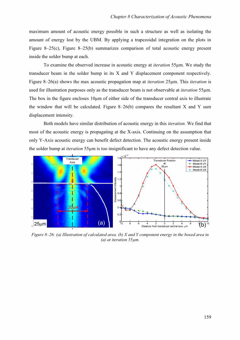
Chapter 8 Characterization of Acoustic Phenomena
159
maximum amount of acoustic energy possible in such a structure as well as isolating the
amount of energy lost by the UBM. By applying a trapezoidal integration on the plots in
Figure 8–25(c), Figure 8–25(b) summarizes comparison of total acoustic energy present
inside the solder bump at each.
To examine the observed increase in acoustic energy at iteration 55µm. We study the
transducer beam in the solder bump in its X and Y displacement component respectively.
Figure 8–26(a) shows the max acoustic propagation map at iteration 25µm. This iteration is
used for illustration purposes only as the transducer beam is not observable at iteration 55µm.
The box in the figure encloses 10µm of either side of the transducer central axis to illustrate
the window that will be calculated. Figure 8–26(b) compares the resultant X and Y sum
displacement intensity.
Both models have similar distribution of acoustic energy in this iteration. We find that
most of the acoustic energy is propagating at the X-axis. Continuing on the assumption that
only Y-Axis acoustic energy can benefit defect detection. The acoustic energy present inside
the solder bump at iteration 55µm is too insignificant to have any defect detection value.
Figure 8–26: (a) Illustration of calculated area. (b) X and Y component energy in the boxed area in
(a) at iteration 55µm.
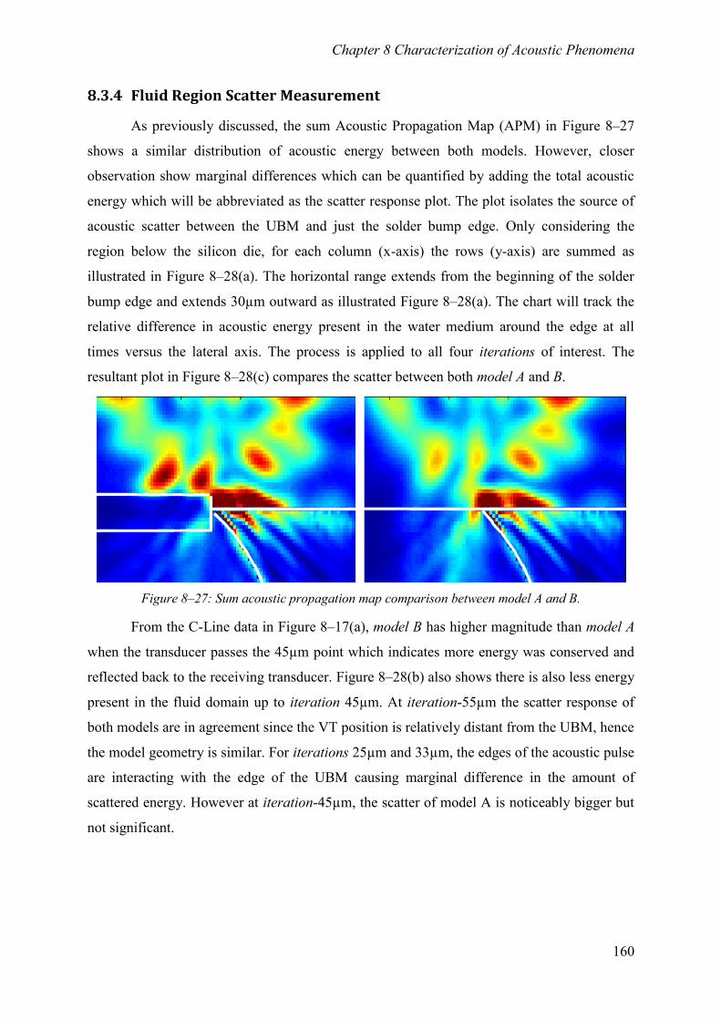
Chapter 8 Characterization of Acoustic Phenomena
160
8.3.4 Fluid Region Scatter Measurement
As previously discussed, the sum Acoustic Propagation Map (APM) in Figure 8–27
shows a similar distribution of acoustic energy between both models. However, closer
observation show marginal differences which can be quantified by adding the total acoustic
energy which will be abbreviated as the scatter response plot. The plot isolates the source of
acoustic scatter between the UBM and just the solder bump edge. Only considering the
region below the silicon die, for each column (x-axis) the rows (y-axis) are summed as
illustrated in Figure 8–28(a). The horizontal range extends from the beginning of the solder
bump edge and extends 30µm outward as illustrated Figure 8–28(a). The chart will track the
relative difference in acoustic energy present in the water medium around the edge at all
times versus the lateral axis. The process is applied to all four iterations of interest. The
resultant plot in Figure 8–28(c) compares the scatter between both model A and B.
Figure 8–27: Sum acoustic propagation map comparison between model A and B.
From the C-Line data in Figure 8–17(a), model B has higher magnitude than model A
when the transducer passes the 45µm point which indicates more energy was conserved and
reflected back to the receiving transducer. Figure 8–28(b) also shows there is also less energy
present in the fluid domain up to iteration 45µm. At iteration-55µm the scatter response of
both models are in agreement since the VT position is relatively distant from the UBM, hence
the model geometry is similar. For iterations 25µm and 33µm, the edges of the acoustic pulse
are interacting with the edge of the UBM causing marginal difference in the amount of
scattered energy. However at iteration-45µm, the scatter of model A is noticeably bigger but
not significant.
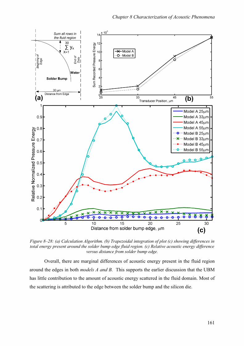
Chapter 8 Characterization of Acoustic Phenomena
161
Figure 8–28: (a) Calculation Algorithm. (b) Trapezoidal integration of plot (c) showing differences in
total energy present around the solder bump edge fluid region. (c) Relative acoustic energy difference
versus distance from solder bump edge.
Overall, there are marginal differences of acoustic energy present in the fluid region
around the edges in both models A and B. This supports the earlier discussion that the UBM
has little contribution to the amount of acoustic energy scattered in the fluid domain. Most of
the scattering is attributed to the edge between the solder bump and the silicon die.
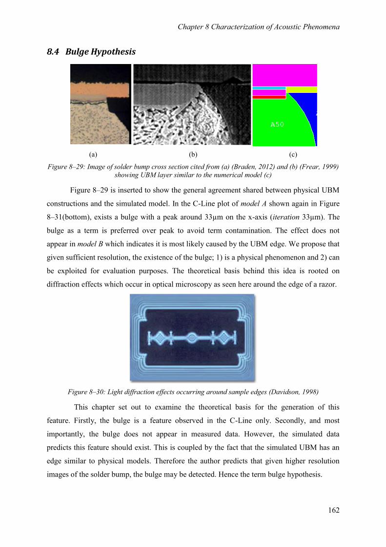
Chapter 8 Characterization of Acoustic Phenomena
162
8.4 Bulge Hypothesis
(a) (b) (c)
Figure 8–29: Image of solder bump cross section cited from (a) (Braden, 2012) and (b) (Frear, 1999)
showing UBM layer similar to the numerical model (c)
Figure 8–29 is inserted to show the general agreement shared between physical UBM
constructions and the simulated model. In the C-Line plot of model A shown again in Figure
8–31(bottom), exists a bulge with a peak around 33µm on the x-axis (iteration 33µm). The
bulge as a term is preferred over peak to avoid term contamination. The effect does not
appear in model B which indicates it is most likely caused by the UBM edge. We propose that
given sufficient resolution, the existence of the bulge; 1) is a physical phenomenon and 2) can
be exploited for evaluation purposes. The theoretical basis behind this idea is rooted on
diffraction effects which occur in optical microscopy as seen here around the edge of a razor.
Figure 8–30: Light diffraction effects occurring around sample edges (Davidson, 1998)
This chapter set out to examine the theoretical basis for the generation of this
feature. Firstly, the bulge is a feature observed in the C-Line only. Secondly, and most
importantly, the bulge does not appear in measured data. However, the simulated data
predicts this feature should exist. This is coupled by the fact that the simulated UBM has an
edge similar to physical models. Therefore the author predicts that given higher resolution
images of the solder bump, the bulge may be detected. Hence the term bulge hypothesis.
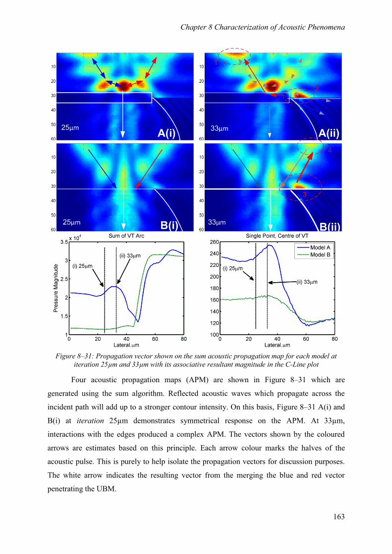
Chapter 8 Characterization of Acoustic Phenomena
163
Figure 8–31: Propagation vector shown on the sum acoustic propagation map for each model at
iteration 25µm and 33µm with its associative resultant magnitude in the C-Line plot
Four acoustic propagation maps (APM) are shown in Figure 8–31 which are
generated using the sum algorithm. Reflected acoustic waves which propagate across the
incident path will add up to a stronger contour intensity. On this basis, Figure 8–31 A(i) and
B(i) at iteration 25µm demonstrates symmetrical response on the APM. At 33µm,
interactions with the edges produced a complex APM. The vectors shown by the coloured
arrows are estimates based on this principle. Each arrow colour marks the halves of the
acoustic pulse. This is purely to help isolate the propagation vectors for discussion purposes.
The white arrow indicates the resulting vector from the merging the blue and red vector
penetrating the UBM.
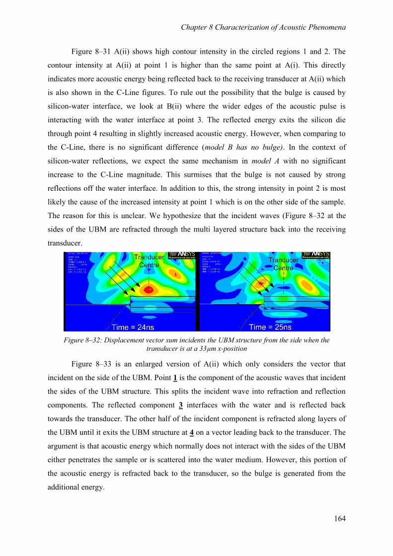
Chapter 8 Characterization of Acoustic Phenomena
164
Figure 8–31 A(ii) shows high contour intensity in the circled regions 1 and 2. The
contour intensity at A(ii) at point 1 is higher than the same point at A(i). This directly
indicates more acoustic energy being reflected back to the receiving transducer at A(ii) which
is also shown in the C-Line figures. To rule out the possibility that the bulge is caused by
silicon-water interface, we look at B(ii) where the wider edges of the acoustic pulse is
interacting with the water interface at point 3. The reflected energy exits the silicon die
through point 4 resulting in slightly increased acoustic energy. However, when comparing to
the C-Line, there is no significant difference (model B has no bulge). In the context of
silicon-water reflections, we expect the same mechanism in model A with no significant
increase to the C-Line magnitude. This surmises that the bulge is not caused by strong
reflections off the water interface. In addition to this, the strong intensity in point 2 is most
likely the cause of the increased intensity at point 1 which is on the other side of the sample.
The reason for this is unclear. We hypothesize that the incident waves (Figure 8–32 at the
sides of the UBM are refracted through the multi layered structure back into the receiving
transducer.
Figure 8–32: Displacement vector sum incidents the UBM structure from the side when the
transducer is at a 33µm x-position
Figure 8–33 is an enlarged version of A(ii) which only considers the vector that
incident on the side of the UBM. Point 1 is the component of the acoustic waves that incident
the sides of the UBM structure. This splits the incident wave into refraction and reflection
components. The reflected component 3 interfaces with the water and is reflected back
towards the transducer. The other half of the incident component is refracted along layers of
the UBM until it exits the UBM structure at 4 on a vector leading back to the transducer. The
argument is that acoustic energy which normally does not interact with the sides of the UBM
either penetrates the sample or is scattered into the water medium. However, this portion of
the acoustic energy is refracted back to the transducer, so the bulge is generated from the
additional energy.
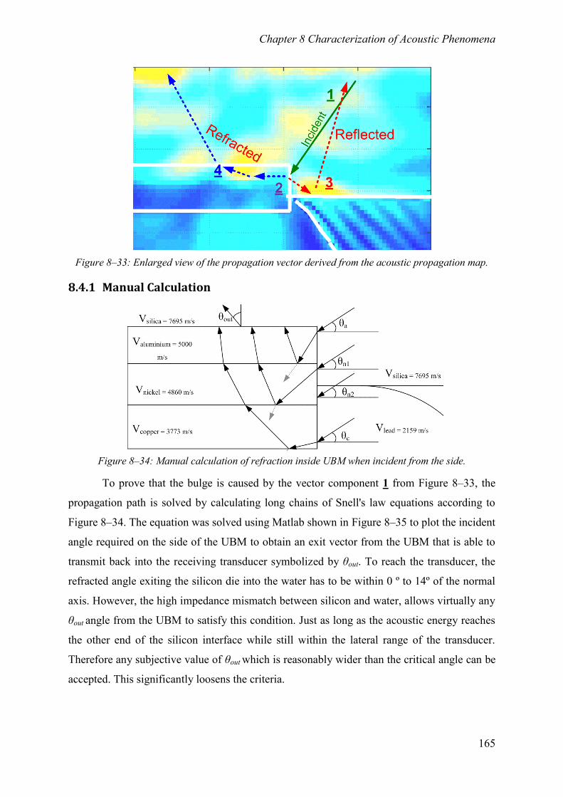
Chapter 8 Characterization of Acoustic Phenomena
165
Figure 8–33: Enlarged view of the propagation vector derived from the acoustic propagation map.
8.4.1 Manual Calculation
Figure 8–34: Manual calculation of refraction inside UBM when incident from the side.
To prove that the bulge is caused by the vector component 1 from Figure 8–33, the
propagation path is solved by calculating long chains of Snell's law equations according to
Figure 8–34. The equation was solved using Matlab shown in Figure 8–35 to plot the incident
angle required on the side of the UBM to obtain an exit vector from the UBM that is able to
transmit back into the receiving transducer symbolized by θout. To reach the transducer, the
refracted angle exiting the silicon die into the water has to be within 0 º to 14º of the normal
axis. However, the high impedance mismatch between silicon and water, allows virtually any
θout angle from the UBM to satisfy this condition. Just as long as the acoustic energy reaches
the other end of the silicon interface while still within the lateral range of the transducer.
Therefore any subjective value of θout which is reasonably wider than the critical angle can be
accepted. This significantly loosens the criteria.
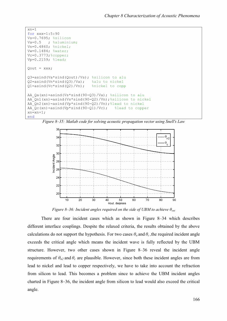
Chapter 8 Characterization of Acoustic Phenomena
166
xn=1
for xxx=1:5:90
Vs=0.7695; %silicon
Va=0.5 ; %aluminium;
Vn=0.4860; %nickel;
Vw=0.1484; %water;
Vc=0.3773;%copper;
Vp=0.2159; %lead;
Qout = xxx;
Q3=asind(Va*sind(Qout)/Vs); %silicon to alu
Q2=asind(Vn*sind(Q3)/Va); %alu to nickel
Q1=asind(Vc*sind(Q2)/Vn); %nickel to copp
AA_Qa(xn)=asind(Vs*sind(90-Q3)/Va); %silicon to alu
AA_Qn1(xn)=asind(Vs*sind(90-Q2)/Vn);%silicon to nickel
AA_Qn2(xn)=asind(Vp*sind(90-Q2)/Vn);%lead to nickel
AA_Qc(xn)=asind(Vp*sind(90-Q1)/Vc); %lead to copper
xn=xn+1;
end
Figure 8–35: Matlab code for solving acoustic propagation vector using Snell's Law
Figure 8–36: Incident angles required on the side of UBM to achieve θout
There are four incident cases which as shown in Figure 8–34 which describes
different interface couplings. Despite the relaxed criteria, the results obtained by the above
calculations do not support the hypothesis. For two cases θa and θc ,the required incident angle
exceeds the critical angle which means the incident wave is fully reflected by the UBM
structure. However, two other cases shown in Figure 8–36 reveal the incident angle
requirements of θn2 and θc are plausible. However, since both these incident angles are from
lead to nickel and lead to copper respectively, we have to take into account the refraction
from silicon to lead. This becomes a problem since to achieve the UBM incident angles
charted in Figure 8–36, the incident angle from silicon to lead would also exceed the critical
angle.
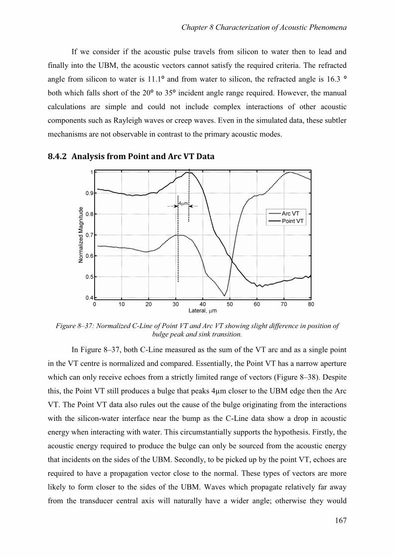
Chapter 8 Characterization of Acoustic Phenomena
167
If we consider if the acoustic pulse travels from silicon to water then to lead and
finally into the UBM, the acoustic vectors cannot satisfy the required criteria. The refracted
angle from silicon to water is 11.1º and from water to silicon, the refracted angle is 16.3 º
both which falls short of the 20º to 35º incident angle range required. However, the manual
calculations are simple and could not include complex interactions of other acoustic
components such as Rayleigh waves or creep waves. Even in the simulated data, these subtler
mechanisms are not observable in contrast to the primary acoustic modes.
8.4.2 Analysis from Point and Arc VT Data
Figure 8–37: Normalized C-Line of Point VT and Arc VT showing slight difference in position of
bulge peak and sink transition.
In Figure 8–37, both C-Line measured as the sum of the VT arc and as a single point
in the VT centre is normalized and compared. Essentially, the Point VT has a narrow aperture
which can only receive echoes from a strictly limited range of vectors (Figure 8–38). Despite
this, the Point VT still produces a bulge that peaks 4µm closer to the UBM edge then the Arc
VT. The Point VT data also rules out the cause of the bulge originating from the interactions
with the silicon-water interface near the bump as the C-Line data show a drop in acoustic
energy when interacting with water. This circumstantially supports the hypothesis. Firstly, the
acoustic energy required to produce the bulge can only be sourced from the acoustic energy
that incidents on the sides of the UBM. Secondly, to be picked up by the point VT, echoes are
required to have a propagation vector close to the normal. These types of vectors are more
likely to form closer to the sides of the UBM. Waves which propagate relatively far away
from the transducer central axis will naturally have a wider angle; otherwise they would
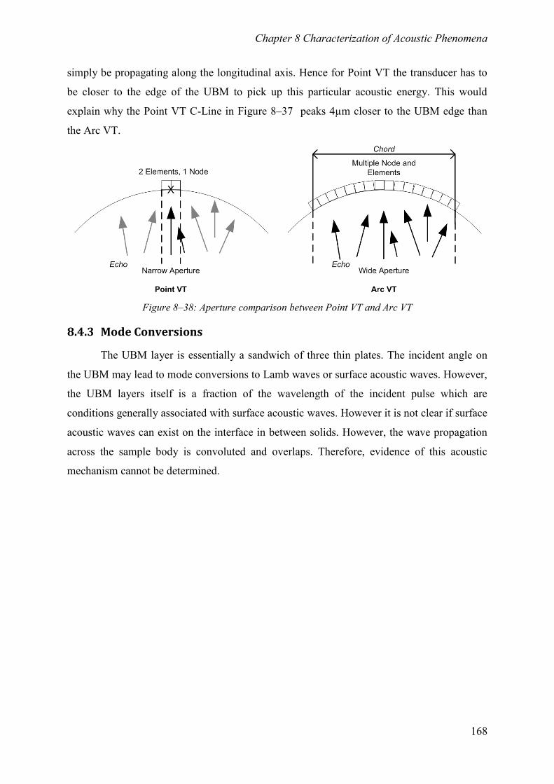
Chapter 8 Characterization of Acoustic Phenomena
168
simply be propagating along the longitudinal axis. Hence for Point VT the transducer has to
be closer to the edge of the UBM to pick up this particular acoustic energy. This would
explain why the Point VT C-Line in Figure 8–37 peaks 4µm closer to the UBM edge than
the Arc VT.
Figure 8–38: Aperture comparison between Point VT and Arc VT
8.4.3 Mode Conversions
The UBM layer is essentially a sandwich of three thin plates. The incident angle on
the UBM may lead to mode conversions to Lamb waves or surface acoustic waves. However,
the UBM layers itself is a fraction of the wavelength of the incident pulse which are
conditions generally associated with surface acoustic waves. However it is not clear if surface
acoustic waves can exist on the interface in between solids. However, the wave propagation
across the sample body is convoluted and overlaps. Therefore, evidence of this acoustic
mechanism cannot be determined.
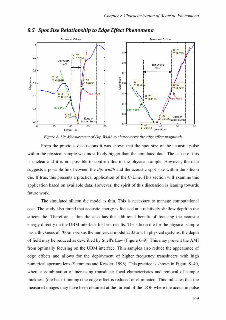
Chapter 8 Characterization of Acoustic Phenomena
169
8.5 Spot Size Relationship to Edge Effect Phenomena
Figure 8–39: Measurement of Dip Width to characterize the edge effect magnitude
From the previous discussions it was shown that the spot size of the acoustic pulse
within the physical sample was most likely bigger than the simulated data. The cause of this
is unclear and it is not possible to confirm this in the physical sample. However, the data
suggests a possible link between the dip width and the acoustic spot size within the silicon
die. If true, this presents a practical application of the C-Line. This section will examine this
application based on available data. However, the spirit of this discussion is leaning towards
future work.
The simulated silicon die model is thin. This is necessary to manage computational
cost. The study also found that acoustic energy is focused at a relatively shallow depth in the
silicon die. Therefore, a thin die also has the additional benefit of focusing the acoustic
energy directly on the UBM interface for best results. The silicon die for the physical sample
has a thickness of 700µm versus the numerical model at 33µm. In physical systems, the depth
of field may be reduced as described by Snell's Law (Figure 6–9). This may prevent the AMI
from optimally focusing on the UBM interface. Thin samples also reduce the appearance of
edge effects and allows for the deployment of higher frequency transducers with high
numerical aperture lens (Semmens and Kessler, 1998). This practice is shown in Figure 8–40,
where a combination of increasing transducer focal characteristics and removal of sample
thickness (die back thinning) the edge effect is reduced or eliminated. This indicates that the
measured images may have been obtained at the far end of the DOF where the acoustic pulse
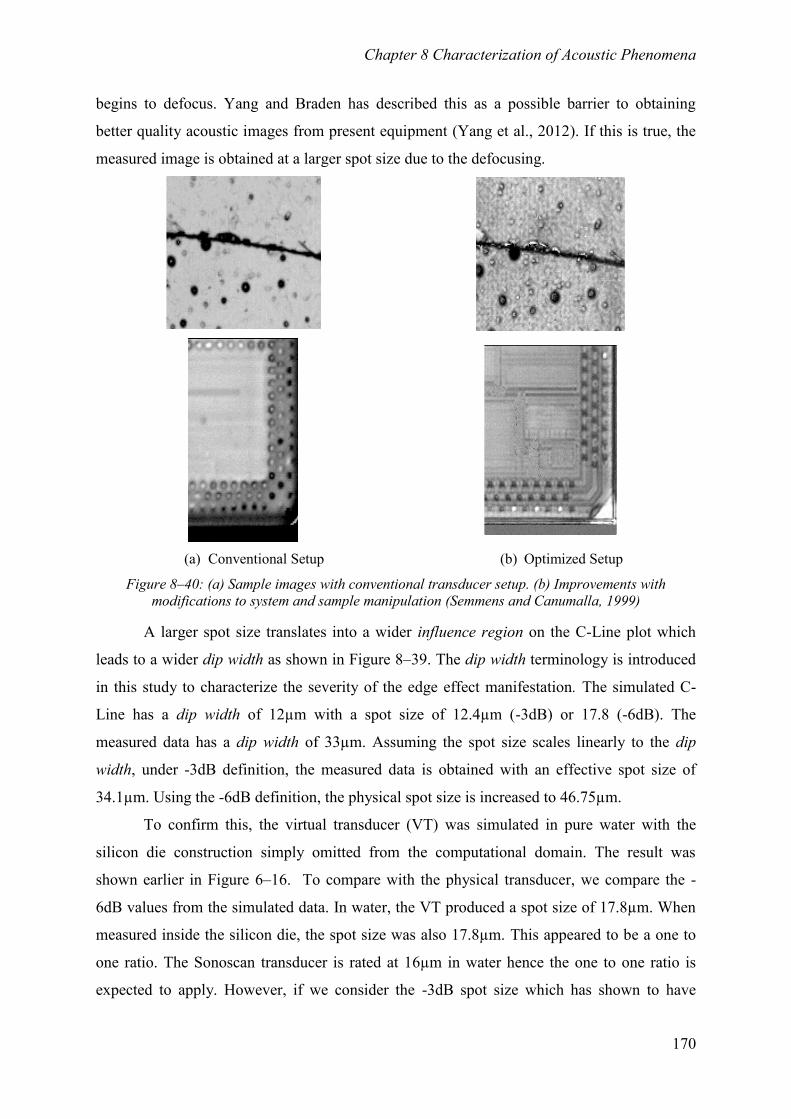
Chapter 8 Characterization of Acoustic Phenomena
170
begins to defocus. Yang and Braden has described this as a possible barrier to obtaining
better quality acoustic images from present equipment (Yang et al., 2012). If this is true, the
measured image is obtained at a larger spot size due to the defocusing.
(a) Conventional Setup (b) Optimized Setup
Figure 8–40: (a) Sample images with conventional transducer setup. (b) Improvements with
modifications to system and sample manipulation (Semmens and Canumalla, 1999)
A larger spot size translates into a wider influence region on the C-Line plot which
leads to a wider dip width as shown in Figure 8–39. The dip width terminology is introduced
in this study to characterize the severity of the edge effect manifestation. The simulated C-
Line has a dip width of 12µm with a spot size of 12.4µm (-3dB) or 17.8 (-6dB). The
measured data has a dip width of 33µm. Assuming the spot size scales linearly to the dip
width, under -3dB definition, the measured data is obtained with an effective spot size of
34.1µm. Using the -6dB definition, the physical spot size is increased to 46.75µm.
To confirm this, the virtual transducer (VT) was simulated in pure water with the
silicon die construction simply omitted from the computational domain. The result was
shown earlier in Figure 6–16. To compare with the physical transducer, we compare the -
6dB values from the simulated data. In water, the VT produced a spot size of 17.8µm. When
measured inside the silicon die, the spot size was also 17.8µm. This appeared to be a one to
one ratio. The Sonoscan transducer is rated at 16µm in water hence the one to one ratio is
expected to apply. However, if we consider the -3dB spot size which has shown to have
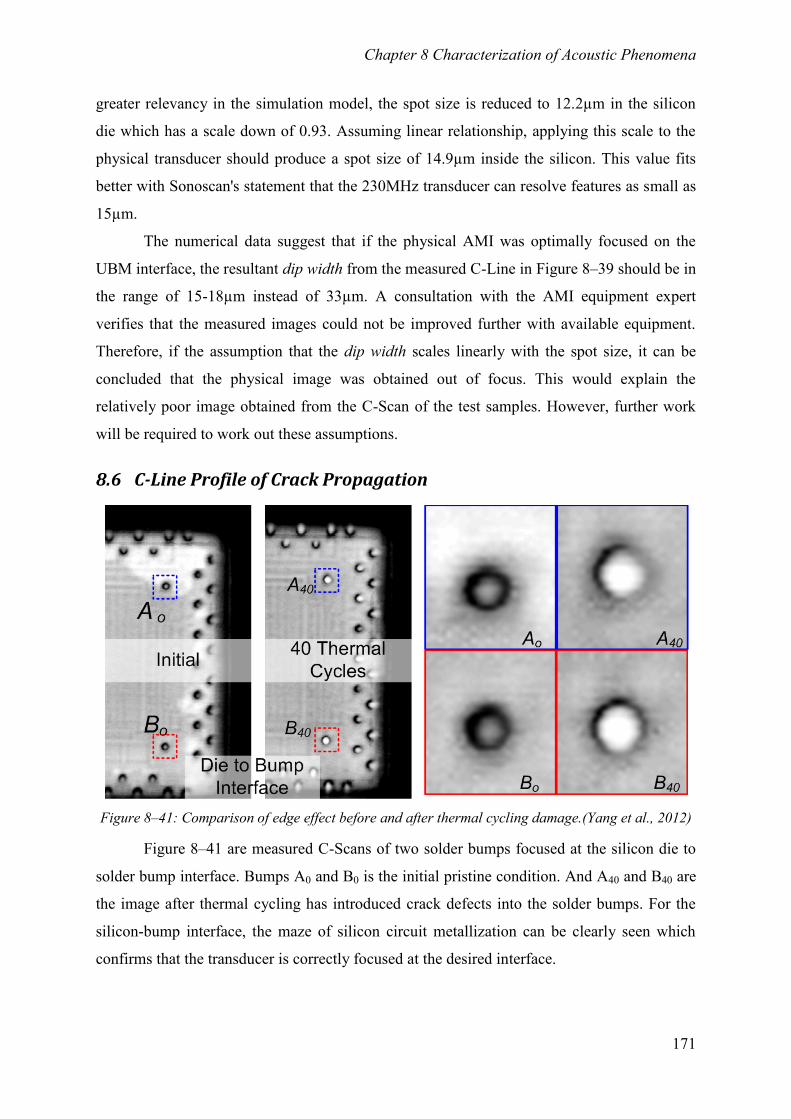
Chapter 8 Characterization of Acoustic Phenomena
171
greater relevancy in the simulation model, the spot size is reduced to 12.2µm in the silicon
die which has a scale down of 0.93. Assuming linear relationship, applying this scale to the
physical transducer should produce a spot size of 14.9µm inside the silicon. This value fits
better with Sonoscan's statement that the 230MHz transducer can resolve features as small as
15µm.
The numerical data suggest that if the physical AMI was optimally focused on the
UBM interface, the resultant dip width from the measured C-Line in Figure 8–39 should be in
the range of 15-18µm instead of 33µm. A consultation with the AMI equipment expert
verifies that the measured images could not be improved further with available equipment.
Therefore, if the assumption that the dip width scales linearly with the spot size, it can be
concluded that the physical image was obtained out of focus. This would explain the
relatively poor image obtained from the C-Scan of the test samples. However, further work
will be required to work out these assumptions.
8.6 C-Line Profile of Crack Propagation
Figure 8–41: Comparison of edge effect before and after thermal cycling damage.(Yang et al., 2012)
Figure 8–41 are measured C-Scans of two solder bumps focused at the silicon die to
solder bump interface. Bumps A0 and B0 is the initial pristine condition. And A40 and B40 are
the image after thermal cycling has introduced crack defects into the solder bumps. For the
silicon-bump interface, the maze of silicon circuit metallization can be clearly seen which
confirms that the transducer is correctly focused at the desired interface.
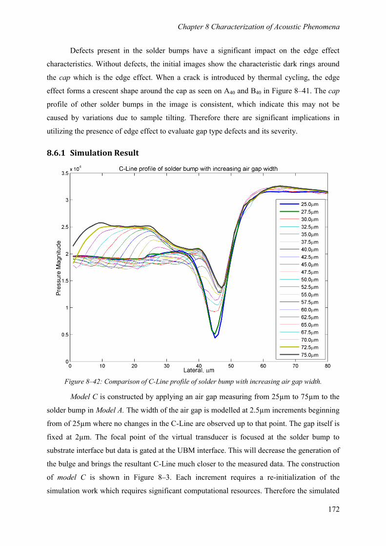
Chapter 8 Characterization of Acoustic Phenomena
172
Defects present in the solder bumps have a significant impact on the edge effect
characteristics. Without defects, the initial images show the characteristic dark rings around
the cap which is the edge effect. When a crack is introduced by thermal cycling, the edge
effect forms a crescent shape around the cap as seen on A40 and B40 in Figure 8–41. The cap
profile of other solder bumps in the image is consistent, which indicate this may not be
caused by variations due to sample tilting. Therefore there are significant implications in
utilizing the presence of edge effect to evaluate gap type defects and its severity.
8.6.1 Simulation Result
Figure 8–42: Comparison of C-Line profile of solder bump with increasing air gap width.
Model C is constructed by applying an air gap measuring from 25µm to 75µm to the
solder bump in Model A. The width of the air gap is modelled at 2.5µm increments beginning
from of 25µm where no changes in the C-Line are observed up to that point. The gap itself is
fixed at 2µm. The focal point of the virtual transducer is focused at the solder bump to
substrate interface but data is gated at the UBM interface. This will decrease the generation of
the bulge and brings the resultant C-Line much closer to the measured data. The construction
of model C is shown in Figure 8–3. Each increment requires a re-initialization of the
simulation work which requires significant computational resources. Therefore the simulated
Chapter 8 Characterization of Acoustic Phenomena
173
transducer scanning is done at 2µm steps to reduce the load and extrapolated from there. A
total of 21 result sets of model C were obtained, each representing a gradual increase of the
air gap lateral width. This will emulate the propagation of a crack due to mechanical fatigue.
In total, this simulated required 4 weeks continuous run on a single terminal. This does not
include coding and analysis time.
For each set, a single C-Line is extracted using the arc VT method. This method sums
all pressure data detected at the entire arc of the VT. All resultant 21 C-Lines are placed
plotted in Figure 8–42 a change in C-Line profile for each air gap width. The thicker lines are
shown to indicate the beginning and the end of the air gap width iterations. The plot clearly
shows that the progress of the crack propagation is reflected in the C-Line profile in a
consistent manner.
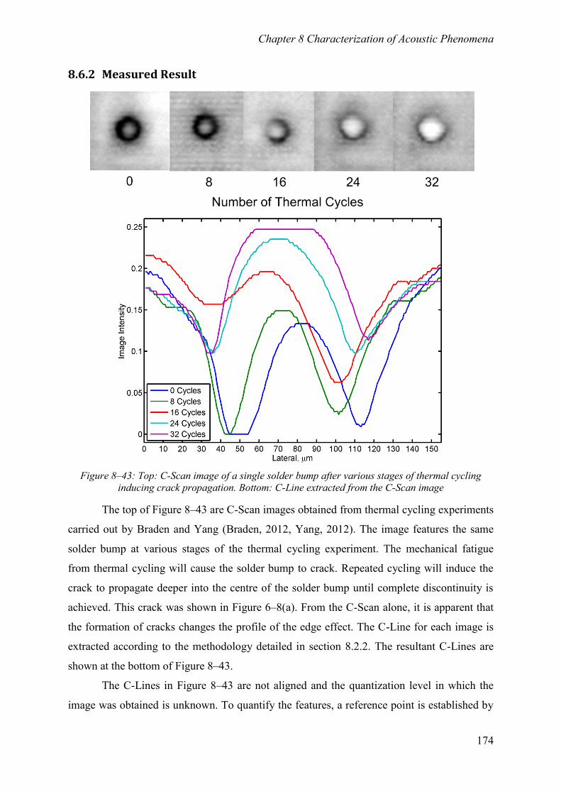
Chapter 8 Characterization of Acoustic Phenomena
174
8.6.2 Measured Result
Figure 8–43: Top: C-Scan image of a single solder bump after various stages of thermal cycling
inducing crack propagation. Bottom: C-Line extracted from the C-Scan image
The top of Figure 8–43 are C-Scan images obtained from thermal cycling experiments
carried out by Braden and Yang (Braden, 2012, Yang, 2012). The image features the same
solder bump at various stages of the thermal cycling experiment. The mechanical fatigue
from thermal cycling will cause the solder bump to crack. Repeated cycling will induce the
crack to propagate deeper into the centre of the solder bump until complete discontinuity is
achieved. This crack was shown in Figure 6–8(a). From the C-Scan alone, it is apparent that
the formation of cracks changes the profile of the edge effect. The C-Line for each image is
extracted according to the methodology detailed in section 8.2.2. The resultant C-Lines are
shown at the bottom of Figure 8–43.
The C-Lines in Figure 8–43 are not aligned and the quantization level in which the
image was obtained is unknown. To quantify the features, a reference point is established by
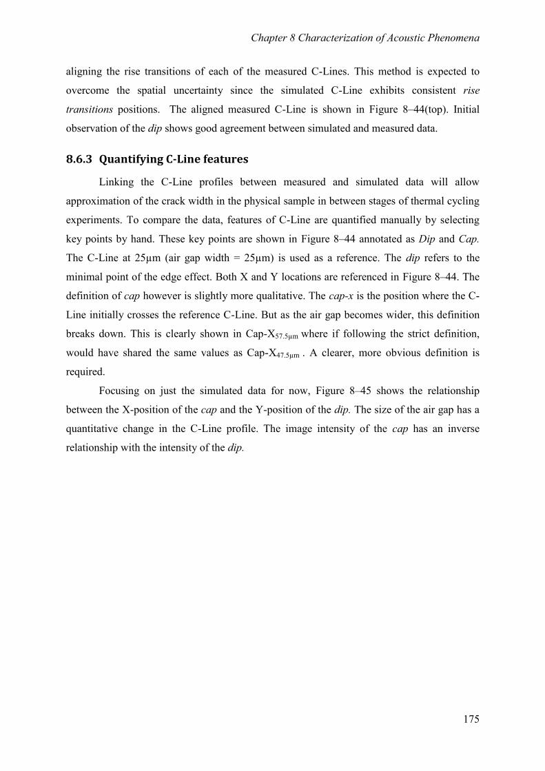
Chapter 8 Characterization of Acoustic Phenomena
175
aligning the rise transitions of each of the measured C-Lines. This method is expected to
overcome the spatial uncertainty since the simulated C-Line exhibits consistent rise
transitions positions. The aligned measured C-Line is shown in Figure 8–44(top). Initial
observation of the dip shows good agreement between simulated and measured data.
8.6.3 Quantifying C-Line features
Linking the C-Line profiles between measured and simulated data will allow
approximation of the crack width in the physical sample in between stages of thermal cycling
experiments. To compare the data, features of C-Line are quantified manually by selecting
key points by hand. These key points are shown in Figure 8–44 annotated as Dip and Cap.
The C-Line at 25µm (air gap width = 25µm) is used as a reference. The dip refers to the
minimal point of the edge effect. Both X and Y locations are referenced in Figure 8–44. The
definition of cap however is slightly more qualitative. The cap-x is the position where the C-
Line initially crosses the reference C-Line. But as the air gap becomes wider, this definition
breaks down. This is clearly shown in Cap-X57.5µm where if following the strict definition,
would have shared the same values as Cap-X47.5µm . A clearer, more obvious definition is
required.
Focusing on just the simulated data for now, Figure 8–45 shows the relationship
between the X-position of the cap and the Y-position of the dip. The size of the air gap has a
quantitative change in the C-Line profile. The image intensity of the cap has an inverse
relationship with the intensity of the dip.
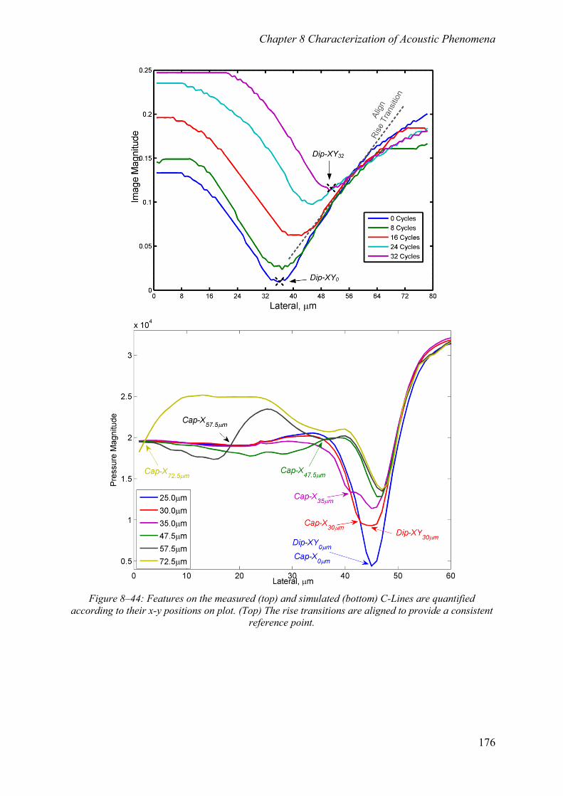
Chapter 8 Characterization of Acoustic Phenomena
176
Figure 8–44: Features on the measured (top) and simulated (bottom) C-Lines are quantified
according to their x-y positions on plot. (Top) The rise transitions are aligned to provide a consistent
reference point.
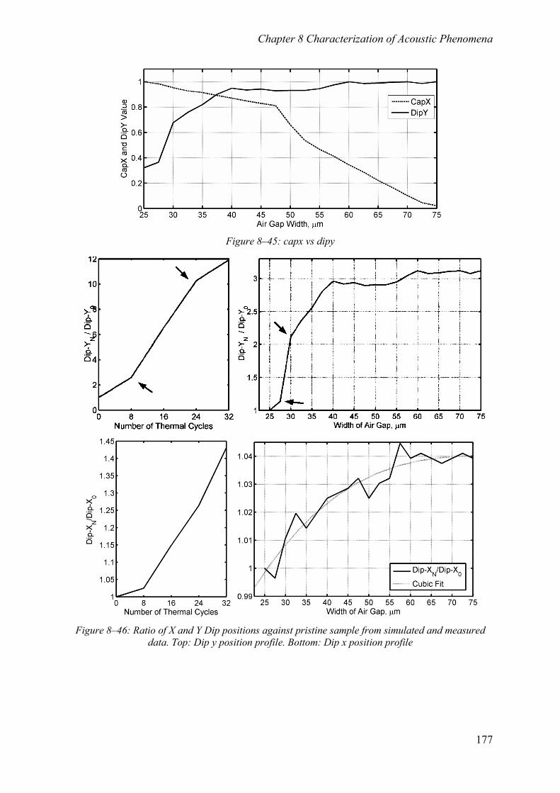
Chapter 8 Characterization of Acoustic Phenomena
177
Figure 8–45: capx vs dipy
Figure 8–46: Ratio of X and Y Dip positions against pristine sample from simulated and measured
data. Top: Dip y position profile. Bottom: Dip x position profile
Chapter 8 Characterization of Acoustic Phenomena
178
Accurate alignment of the measured data is necessary to obtain conclusive data.
However, in this study, the measured data was not obtained with this work in mind. Therefore
the inference and assumptions required will only allow a preliminary study. Therefore, in
light of alignment uncertainty, the best recourse is to base the analysis on the changes in C-
Line features against a C-Line profile without air gaps. The changes can be quantified and
preliminary conclusions can be drawn.
The dip and cap values from the initial C-Line of their respective data source are used
as reference points. Figure 8–46 is created by dividing the subsequent dip and cap values of
C-Lines with air gaps with the reference value to establish a ratio. This is expected to
normalize the resultant plot of both data sources to the same scale as the feature changes are
relative to the pristine example. The resultant ratio profiles are comparable. The top of Figure
8–46 is obtained using the Y-Axis ratio of the dip points. While the lower figure uses the dip
X-axis. Cap-X data is not available as the measured C-Line with defects did not intersect the
reference C-Line. In addition, the ratio produced by the measured data is higher than the
simulated counterpart. This might be attributed to non-linear quantization by the AMI
equipment.
At 32 thermal cycles shown at the top of Figure 8–46, the width of the crack is
approximated have a horizontal width of between 30µm to 40µm. This is solely based on
referencing the simulated data. The plot also evens out beyond 40µm which prevents
characterization if the crack is longer. Another limitation relies on the acquisition of the
measured data which appears to be clipped. A limited data sample between thermal cycles
from the measured data prevents firmer conclusions. Figure 8–46(bottom) is constructed from
irregular data which may be manifested from poor scanning resolution from the simulation
execution. Cubic curve fitting is employed to average the data points. From the fitted plot, the
gradients are comparable up to 45µm. No other obvious correlations are observed.
8.6.4 Discussions
The effect of crack propagation on the C-Line profile is a unique study. There are
limitations in both the simulated and measured data. Therefore this section was presented as a
preliminary investigation to make fundamental discoveries and help inform further work.
Comprehensive analysis will require repeating the thermal cycling test with more stringent
parameters. In the thermal cycling experiment, the boards are monitored every 8 cycles.
However, a non-linear relationship between the dip and cap versus the width of the air gap is
Chapter 8 Characterization of Acoustic Phenomena
179
observed in the simulated data. Therefore shorter monitoring cycles are desired especially
during the initiation phase of the defect.
Crack initiations usually originate from the outer parameter of the solder bump (Yang,
2012) which is the focus of this study. Other types of defects like voids and on rare
occasions, the cracks initiated from the centre of the solder bump will provide another set of
C-Line profiles. The C-Line profile of more comprehensive variety of defect types was
recommended for further work.
The measured C-Line shows clipping around the peak as well as the dip. Widening
and standardizing the quantization levels of the AMI system is required to provide a reliable
reference magnitude to align multiple C-Lines together. In the physical experiment, a heavy
metal bracket is used to hold the sample during C-Scan acquisition. This allows the
transducer Z-axis focal position to be remembered and repeated. Therefore the issue is mainly
related to the analogue to digital conversion threshold and gating.
In the simulated data, the rise transition reliably indicates the position where the
silicon-water interface begins. From that, we infer that the rise transition seen in the
measured data is equally consistent which allows for lateral (x-axis) alignment of the
measured data. This inference is justified based on the fact that the rise transition is generated
from initial contact with the silicon-water interface which has a high impedance mismatch.
Ideally, there should be a physical marker that can be observed in the C-Scan image. It is also
unfeasible to use native features like die edges as these are susceptible to the edge effects that
cause wide image intensity gradients (smudges). This problem is exacerbated by relatively
low scanning resolutions of 8µm per pixel.
The novel C-Line plot was proposed as a robust tool to characterize the features
caused by the edge effect mechanisms. However, obtaining the simulated data required 3
terminals and a total of 1400 hours of run time. In the simulated data, the spatial density of
the buffer regions was lowered aggressively (5 elements per wavelength) and the scanning
resolution was done at 2µm intervals. This compromise is reflected in Figure 8–46 where the
Dip-X ratios were relatively erratic. Given that newer version of ANSYS can utilize the
processors from graphic cards, more comprehensive simulations can be carried out in further
work.

Chapter 9 Summary and Conclusion
180
Chapter 9
Conclusion
Chapter 9 Summary and Conclusion
181
9 Summary and Conclusion
This thesis details the methodology for a high frequency transient simulation in a
micro scale environment of advanced electronic packaging technologies. This required a solid
multidisciplinary background in microelectronic packaging technology and acoustic imaging
technology. Moving the work into the domain of numerical simulations, the finite element
method and its variety of approaches was studied. A preliminary study revealed that the
computing resource required to solve the experiment were beyond the available equipment
capabilities. This led to the development of compromises and techniques which were tested
empirically. With the general methodology firmly established, configurations specific to the
required experiment were evaluated for validity. A firm correlation between simulated and
measured data was achieved. Comprehensive analysis of the experimental data generated
several hypotheses. When possible, supplementary experiments were added to verify or test
the hypotheses with mixed success. The contributions of this study are split into three
sections preceded by a summary of the background.
9.1 Background Summary
The development of complex multilayered microelectronic packages represents a
problem for current acoustic inspection technology that is reaching its resolution limits. This
has led to reliability issues that are particularly important in industries where critical failures
pose a risk to health and safety as well as economic importance to all industries. However,
acoustic inspection remains a most effective means for the detection of void type defects.
However certain key limitations to acoustic inspection include;
Application specific transducers limit flexibility which increases evaluation cost.
While resolution increases with frequency, the penetration capability degrades. The
introduction of stacked die packages exacerbates this issue.
The manifestation of edge effect phenomena prevents direct evaluation of edge
regions of the sample.
To overcome such limitations without introducing hardware modifications, various
algorithms were developed. One key recent development is the sparse representation method.
This advanced algorithm partly relies on a priori information to build up a dictionary.
However, the acoustic propagation mechanisms in complex microelectronic packages are not
clearly understood. Simulated data may have important implications for this technique in
future work.
Chapter 9 Summary and Conclusion
182
9.2 Contributions to Finite Element Methodology
There are many options and approaches to constructing a numerical simulation. This
process is mainly reflected by the governing equations and they are used. For the simulation
work, the experiment was carried out using a full transient method. This method was
computationally expensive, but has no risk of missing physical phenomena, as all terms in the
governing equations are calculated. Preliminary work applied an impact load to a piece of
aluminium block to observe the resultant S, P and R waves, which were all present. This
verified the basic transient simulation setup. Data from the primary simulation work on the
solder bump assembly showed agreement with measured data.
9.2.1 Evaluation of Numerical Dispersion Error
It is a widely held view that a temporal and spatial resolution of both 20 elements and
time steps per wavelength are required to suppress numerical dispersion errors. However, the
increased spatial resolution produced a quadratic increase to computational cost, while
increasing temporal resolution had a linear cost increase. The performances of the solution
convergence of these parameters are tested. An elaborate study covering a wide spectrum of
spatial and temporal combinations was tested to evaluate the numerical dispersion error. This
study concluded that;
20 elements per wavelength has a correlation 0.99 compared to the control result
15 elements per wavelength has a correlation of 0.95 compared to the control result
There was no significant increase in fidelity beyond 20 elements per wavelength
15 elements per wavelength is significantly cheaper to compute
A temporal resolution of 15 is acceptable and 20 are recommended. Computational
cost increase is linear.
9.2.2 Development of Quadrilateral Infinite Boundary
The literature review shows that the realization of an ideal absorbing boundary
condition is impractical. "Local" techniques are introduced to approximate the
absorbing boundary namely;
The Infinite Boundary approach, which asymptotically propagates the waves to
infinity
The Perfectly Matched Layer technique, which unphysically suppresses the wave
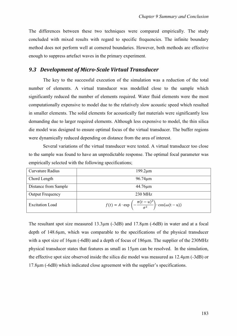
Chapter 9 Summary and Conclusion
183
The differences between these two techniques were compared empirically. The study
concluded with mixed results with regard to specific frequencies. The infinite boundary
method does not perform well at cornered boundaries. However, both methods are effective
enough to suppress artefact waves in the primary experiment.
9.3 Development of Micro-Scale Virtual Transducer
The key to the successful execution of the simulation was a reduction of the total
number of elements. A virtual transducer was modelled close to the sample which
significantly reduced the number of elements required. Water fluid elements were the most
computationally expensive to model due to the relatively slow acoustic speed which resulted
in smaller elements. The solid elements for acoustically fast materials were significantly less
demanding due to larger required elements. Although less expensive to model, the thin silica
die model was designed to ensure optimal focus of the virtual transducer. The buffer regions
were dynamically reduced depending on distance from the area of interest.
Several variations of the virtual transducer were tested. A virtual transducer too close
to the sample was found to have an unpredictable response. The optimal focal parameter was
empirically selected with the following specifications;
Curvature Radius 199.2µm
Chord Length 96.74µm
Distance from Sample 44.76µm
Output Frequency 230 MHz
Excitation Load
The resultant spot size measured 13.3µm (-3dB) and 17.8µm (-6dB) in water and at a focal
depth of 148.6µm, which was comparable to the specifications of the physical transducer
with a spot size of 16µm (-6dB) and a depth of focus of 186µm. The supplier of the 230MHz
physical transducer states that features as small as 15µm can be resolved. In the simulation,
the effective spot size observed inside the silica die model was measured as 12.4µm (-3dB) or
17.8µm (-6dB) which indicated close agreement with the supplier’s specifications.
Chapter 9 Summary and Conclusion
184
9.4 Contribution to Post Processing Techniques
9.4.1 C-Line Plot
The C-Line plot was introduced as a novel post processing tool for the
characterization of the edge effect phenomena. The key strength of the C-Line plot is the
relatively simple application technique. Application of this methodology allows the edge
effect manifestation to be quantified and opens new avenues for evaluation and research. The
changes of acoustic response due to feature transitions are marked by gradient changes in the
C-Line plot. These changes have strong correlations with the 12.4µm (-3dB) spot size
definition.
The method also found that rise transitions are a good indicator of solder bump
spatial position. By aligning the rise transitions, the centre of the solder bump from C-Scan
images can be determined more systematically.
9.4.2 Acoustic Propagation Map
The simulation produced X, Y and vector sum displacements in solids as well as
pressure data in the fluid region. The pressure response from the virtual transducer is
equivalent to that of physical systems. The C-Line was derived from this data type. Transient
pressure and displacement data were merged into cross sectional slides for qualitative
evaluation of the acoustic wave propagation process. Through post processing methods, these
two different data types were consolidated into a single image.
The acoustic propagation map was introduced by merging the slides using either max
or sum numerical algorithms. The acoustic propagation map shows in one picture the
distribution of acoustic energy at various transducer positions. Combining the analysis from
the C-Line, transient slides and acoustic propagation maps various observations were drawn.
Chapter 9 Summary and Conclusion
185
9.5 Contribution to Theory
9.5.1 Horizontal Scatter
The C-Line plot and the acoustic propagation map were cross analysed with the
following findings;
A significant portion of the acoustic energy was reflected by the UBM interface.
When the transducer was positioned at the "solder bump - silica die" edge, a large
portion of the energy was refracted along the silica-water interface, aptly named
"horizontal scatter".
The horizontal scatter mechanism occurs regardless of the presence of the UBM.
Absence of an UBM in the solder joint assembly will eliminate the presence of edge
effects
The edge effect generation on the C-Line is annotated as the dip which is the minimum
magnitude on the C-Line profile. Despite the edge effect, the drop in acoustic energy was
governed by a lower limit indicating that not all the acoustic energy was lost. On the acoustic
propagation map, the horizontal scatter was only observed when the centre of the transducer
was around the dip. This concludes that in addition to loss through scattering, a large amount
of acoustic energy was lost through horizontal scattering.
9.5.2 The Bulge
The numerical simulation predicts the existence of features that do not appear in the
measured data. This was due to the low resolution of the experimentally measured image,
which on paper is only able to resolve features as small as 15µm. This makes verification
difficult. The C-Line profile showed a ‘bulge’, which occurred when the transducer was
focused closed to the UBM edge. The bulge was not present in Model B, which does not have
a UBM. The hypothesis proposed here is that given improved AMI resolution, the bulge
would be experimentally observed. With the bulge present, it will mark the boundaries of the
UBM which benefits image evaluation. However, manual calculations could not confirm the
source of this phenomenon. Using the point VT data to restrict the aperture of the receiving
virtual transducer, it was observed that the source of the bulge originated very close to the
UBM edge.
Chapter 9 Summary and Conclusion
186
9.5.3 Scatter Plot
The scatter plot measured the relative amount of acoustic energy present in
1. The Fluid region around the edge of the "solder bump - silica die"
The plot showed that the presence of the UBM marginally increased the amount of acoustic
energy scattered into the fluid domain. The majority of the scattered energy was caused by
the “solder bump –silica die” edge.
2. The solder bump
Measurements of the displacement energy inside the solder bump showed that without the
UBM present, acoustic energy penetrating into the solder bump is 31.9% to 44% higher than
is the case when the UBM is present. However, it also showed that at iteration 55µm, Y-Axis
acoustic energy is insignificant. In the context of C-scan images, this means the outer radius
of the solder bump cannot be evaluated reliably since no useful acoustic energy was available
for defect detection to occur within the solder bump in the annular region. This will pose
significant problems in detecting the initiation of cracks.
9.5.4 Spot Size Approximation
This study proposed that the gap of the edge effect called the dip width is directly
associated with the effective acoustic spot size occurring within the sample. Assuming that
these parameters have a linear relationship, the dip width and the spot size can be used to
postulate the effective spot size of physical data. Using this approximation with the current
data, it was found that the measured data was obtained with an effective spot size of 33µm, or
46.75µm if the simulated -3dB spot size is used instead. Either consideration was
significantly bigger than the simulated spot size required to resolve features as small as
15µm. The thicker silica dies, may have reduced the depth of field to an extent where the
acoustic pulse was defocused at the desired interface. This idea is consistent with C-Scan
images from thinned die which show C-Scans of solder bumps with thinner edge effect rings
(which translate into narrower dip widths).
Chapter 9 Summary and Conclusion
187
9.5.5 C-Line Profiles in Crack Propagation
The C-Line profile is affected by the presence of crack defects, which are modelled as
air gaps in the solder bump. The change in the profile follows a predictable trend.
Quantification of these profile changes was used to predict the progress of the crack
propagation in physical C-Scan images. The changes in the C-Line profile against linear
increase in air gap width were found to be non-linear. Preliminary work shows that this
methodology is feasible. However, the analysis is only presented as preliminary work, since
the available measured data does not contain enough data points to be conclusive. A firm
observation was that an initiated crack can propagate up to 25µm towards the centre of the
solder bump before a change is observed in the C-Line plot. However, this difference was
detected due to the availability of the reference C-Line for comparison. Actual detection in
physical systems may only be able to differentiate greater crack widths to give noticeable
results.
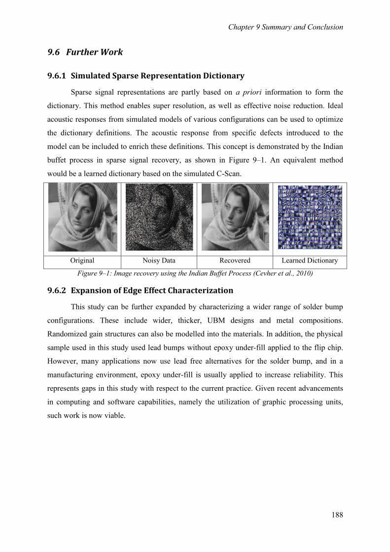
Chapter 9 Summary and Conclusion
188
9.6 Further Work
9.6.1 Simulated Sparse Representation Dictionary
Sparse signal representations are partly based on a priori information to form the
dictionary. This method enables super resolution, as well as effective noise reduction. Ideal
acoustic responses from simulated models of various configurations can be used to optimize
the dictionary definitions. The acoustic response from specific defects introduced to the
model can be included to enrich these definitions. This concept is demonstrated by the Indian
buffet process in sparse signal recovery, as shown in Figure 9–1. An equivalent method
would be a learned dictionary based on the simulated C-Scan.
Original Noisy Data Recovered Learned Dictionary
Figure 9–1: Image recovery using the Indian Buffet Process (Cevher et al., 2010)
9.6.2 Expansion of Edge Effect Characterization
This study can be further expanded by characterizing a wider range of solder bump
configurations. These include wider, thicker, UBM designs and metal compositions.
Randomized gain structures can also be modelled into the materials. In addition, the physical
sample used in this study used lead bumps without epoxy under-fill applied to the flip chip.
However, many applications now use lead free alternatives for the solder bump, and in a
manufacturing environment, epoxy under-fill is usually applied to increase reliability. This
represents gaps in this study with respect to the current practice. Given recent advancements
in computing and software capabilities, namely the utilization of graphic processing units,
such work is now viable.
Chapter 9 Summary and Conclusion
189
9.6.3 Further Analysis of the Bulge
The generation of the bulge may have similar properties to the diffraction effects seen
in optical metrology. The methodologies applied to isolate the cause of this phenomenon
were unconvincing. Manual calculations of the acoustic wave vector could not isolate the
source of the acoustic energy that causes the Bulge. The next recommended step would be to
obtain measured images of a thinned die of the same configuration. This step would however,
destroy the sample, making the method no-longer non-destructive technique. If the bulge
does appear in measured data, further analysis may reveal its use as a new evaluation tool.
9.6.4 Horizontal Scatter
Horizontal scatter was apparent in the acoustic propagation map. Yet, the propagation
mechanism observed in the simulation was complex. Direct tracking of the wave as it
propagates through the sample would clarify the generation mechanism of the horizontal
scatter. It would also improve this field of study by revealing subtler acoustic mechanisms
that may be related to the defect detection mechanism.
9.6.5 Improving Defect Detection Study
One of the limitations of the study presented in Chapter 8.6 was the insufficient
number of data points from the measured data and the compromised simulation fidelity.
Improving the simulation is merely involves the task of increasing resolution and allowing
for more time to solve the simulation (2000 - 3000 hours with the author's equipment).
However, obtaining closer data points for the measured data requires re-initialization of the
thermal cycling experiments. The sample will be required to be scanned at every thermal
cycle, as opposed to every 8 thermal cycles, as collected in the current data. This is crucial
since the defects do not affect the C-Line in a linear fashion. In the context of the C-Line
plot, the first few data points will contain a significant amount of information. When the
sample is being scanned, the quantization settings will have to be fixed to retain consistency.
Preferably, a marker can be introduced into the sample for alignment purposes.
On the simulation side, we found that the defect remains undetected until the crack
has a width of at least 25µm. The next step would be to introduce void type defects at various
positions within the solder bump. The sizes of the void can be increased gradually until a
response from the C-Line is detected. The transducer configuration could be changed as well.
Such a study would provide a guide on the minimal detectable defect size given specific
acoustic setups.
Chapter 9 Summary and Conclusion
190
9.6.6 Evaluation of Under Bump Metallization
In this study, it was found that the UBM structure has a significant impact on the
penetration of acoustic energy. It would be useful then to evaluate various UBM
configurations to find the optimal recipe. This can be done by varying individual thickness of
the UBM layers to vary the concentration. This work may provide useful insight on future
UBM designs. #
9.6.7 Simplify Solder Bump Image using C-Line Plots
As mentioned in 7.2.5, the C-Line plot can be used to create a C-Scan image. Inherent
complexities with measured data make alignment and determination of centre difficult. Since
the position of the rise transition is relatively constant, it can be used for alignment. An
approximate image can then be created from the measured data. This seems counter intuitive
since measured data in its original state are ideal for analysis. However, overcoming
alignment problems can have immense benefits for implementation of algorithms.
For example, multiple C-Lines can be extracted from various axes (diagonal, vertical,
horizontal, etc) of an approximate solder bump location. The image will most likely have an
off-centre cap. The C-Line plot can then be aligned not unlike the methods used in Chapter
8.6.3. The data can then either be averaged or extrapolated along its own sector. E.g. Two C-
Lines from X,Y axis are extrapolated 90º around a central axis to rebuild the C-Scan image.
Depending on the number of C-Lines extracted, the alignment factor is eliminated and work
can be concentrated on the bonding quality.

Appendix
191
Appendix
Appendix
192
10 Appendix
Appendix i: Input File 020B, Plucked Cantilever Beam ........................................................ 195
Appendix ii: Plucked cantilever beam surrounded by air medium ........................................ 195
Appendix iii: Transient Impact Impulse on Solid block ........................................................ 195
Appendix iv: Source Code for Quadrilateral Infinite Absorbing Boundary Technique ........ 195
Appendix v: Source Code for Numerical Dispersion Error Experiment ............................... 195
Appendix vi: Post Processing Source Code: 023Analysis dvd.m ......................................... 195
Appendix vii: Primary Acoustic Mechanism Study Experiment Model A ........................... 195
Appendix viii: Primary Acoustic Mechanism Study Experiment Model B .......................... 195
Appendix ix: Defect Detection Mechanism Experiment (Model C) ..................................... 195
Appendix x: Generation of Acoustic Propagation Map ......................................................... 195
Appendix xi: Simulated C-Scan Algorithm ........................................................................... 195
Appendix xii: All Plots of Sum, X and Y vector components at three key times ................. 196
Appendix xiii: Video of intra sample acoustic propagation at four transducer positions ...... 196
Appendix xiv: X and Y vector component APM of model A,B and C ................................. 197
Appendix xv: Path Operations Raw Data .............................................................................. 197
Appendix xvi: Measured Solder Bump C-Scan and Plot ....................................................... 197
Appendix xvii: Model A and B C-Line Data ......................................................................... 198
Appendix
193
10.1 Publications
1) Development of C-Line Methodology for the Evaluation of Edge Phenomena in
Acoustic Micro Imaging.
Lee, Chean, Zhang, G.M. and Harvey, D.M.
General Engineering Research Institute Annual Research Symposium 2013
Abstract: Acoustic images are no stranger to anomalies and phenomenon which degrade the
image. The understandings of such mechanisms are implied form collective opinions and
seldom empirically verified. Most post processing algorithms are developed to improve the
final acoustic image. But there has been little focus on the study of the acoustic mechanism
inside the sample. With the finite element technique, this has become possible. A novel post
processing methodology is required to interpret and bridge the simulated and measured data.
The C-Line plot is a novel methodology proposes to solve this conundrum. This technique
has shown clear benefits as a supplement to current non-destructive reliability studies.
2) Analysis of solder joint Edge Effect in Acoustic Micro Imaging of
microelectronic packages: A preliminary study
Lee, Chean, Zhang, G.M. and Harvey, D.M. (2012)
Electronic System-Integration Technology Conference (ESTC), 2012 4th
Abstract: A guaranteed occurrence when using Acoustic Micro Imaging, the phenomena
called Edge Effect is not clearly understood. The widely accepted reliance on scatter theory
to explain edge effect is challenged in this study. The edge effect of solder joints is
investigated using finite element modelling. Simulation strategies for reducing computational
load are proposed. A methodology to characterize acoustic data for edge effect analysis is
further developed. Results show that the relationship between scatter theory and edge effect is
not straight forward.
Appendix
194
3) Acoustic Micro Imaging Edge Effect Characterization of 80µm Solder Bump
Flip Chip
Lee, Chean, Zhang, G.M. and Harvey, D.M.
General Engineering Research Institute Annual Research Symposium 2012
Abstract: Acoustic Micro Imaging (AMI) is an established tool for non destructive reliability
evaluation in microelectronic packages. It is especially sensitive for evaluating delaminations
and voids. Most common use of AMI requires an acoustic pulse or echo to be reflected from
the material under evaluation. The performance of an acoustic system is defined by its spot
size, focus depth, focal length and frequency. Spot size defines the lateral diameter of a
focused acoustic beam and the focus depth indicates the axial length in which it remains
focused. Acoustic frequency will directly affect the spot size as well as the penetration vs.
resolution relationship of the system.
4) Acoustic field simulation of electronic package: a preliminary study
Lee, Chean, Zhang, G.M. and Harvey, D.M.
General Engineering Research Institute Annual Research Symposium 2010
Abstract. Acoustic micro imaging has reached resolution limits with the continuous
progression of electronic packages. Acoustic field simulation is used to understand the defect
detection mechanism. The simulation setup methodology and various verification techniques
are outlined. Preliminary results are presented.
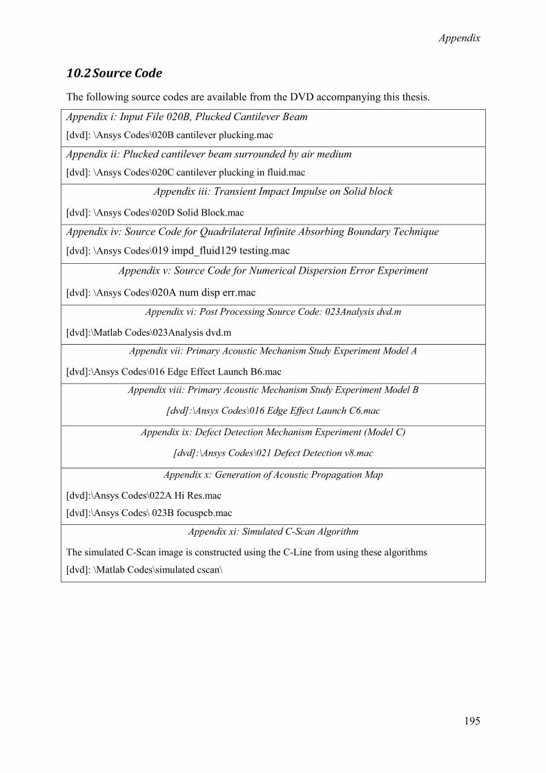
Appendix
195
10.2 Source Code
The following source codes are available from the DVD accompanying this thesis.
Appendix i: Input File 020B, Plucked Cantilever Beam
[dvd]: \Ansys Codes\020B cantilever plucking.mac
Appendix ii: Plucked cantilever beam surrounded by air medium
[dvd]: \Ansys Codes\020C cantilever plucking in fluid.mac
Appendix iii: Transient Impact Impulse on Solid block
[dvd]: \Ansys Codes\020D Solid Block.mac
Appendix iv: Source Code for Quadrilateral Infinite Absorbing Boundary Technique
[dvd]: \Ansys Codes\019 impd_fluid129 testing.mac
Appendix v: Source Code for Numerical Dispersion Error Experiment
[dvd]: \Ansys Codes\020A num disp err.mac
Appendix vi: Post Processing Source Code: 023Analysis dvd.m
[dvd]:\Matlab Codes\023Analysis dvd.m
Appendix vii: Primary Acoustic Mechanism Study Experiment Model A
[dvd]:\Ansys Codes\016 Edge Effect Launch B6.mac
Appendix viii: Primary Acoustic Mechanism Study Experiment Model B
[dvd]:\Ansys Codes\016 Edge Effect Launch C6.mac
Appendix ix: Defect Detection Mechanism Experiment (Model C)
[dvd]:\Ansys Codes\021 Defect Detection v8.mac
Appendix x: Generation of Acoustic Propagation Map
[dvd]:\Ansys Codes\022A Hi Res.mac
[dvd]:\Ansys Codes\ 023B focuspcb.mac
Appendix xi: Simulated C-Scan Algorithm
The simulated C-Scan image is constructed using the C-Line from using these algorithms
[dvd]: \Matlab Codes\simulated cscan\
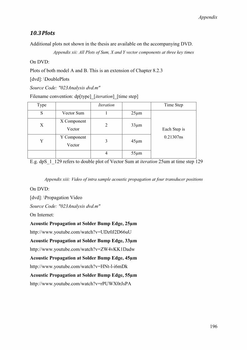
Appendix
196
10.3 Plots
Additional plots not shown in the thesis are available on the accompanying DVD.
Appendix xii: All Plots of Sum, X and Y vector components at three key times
On DVD:
Plots of both model A and B. This is an extension of Chapter 8.2.3
[dvd]: \DoublePlots
Source Code: "023Analysis dvd.m"
Filename convention: dp[type]_[iteration]_[time step]
Type Iteration Time Step
S Vector Sum 1 25µm
Each Step is
0.21307ns
X X Component
Vector 2 33µm
Y Y Component
Vector 3 45µm
4 55µm
E.g. dpS_1_129 refers to double plot of Vector Sum at iteration 25um at time step 129
Appendix xiii: Video of intra sample acoustic propagation at four transducer positions
On DVD:
[dvd]: \Propagation Video
Source Code: "023Analysis dvd.m"
On Internet:
Acoustic Propagation at Solder Bump Edge, 25µm
http://www.youtube.com/watch?v=UDz0J2D66uU
Acoustic Propagation at Solder Bump Edge, 33µm
http://www.youtube.com/watch?v=ZW4vKK1Dadw
Acoustic Propagation at Solder Bump Edge, 45µm
http://www.youtube.com/watch?v=HNt-l-i6mDk
Acoustic Propagation at Solder Bump Edge, 55µm
http://www.youtube.com/watch?v=rPUWX0rJsPA
Appendix
197
Appendix xiv: X and Y vector component APM of model A,B and C
On DVD
[dvd]:\Acoustic Propagation Maps
Source Code: "023Analysis dvd.m"
10.4 Data
Appendix xv: Path Operations Raw Data
On DVD:
Ansys output data for Model A: Nominal Construction
[dvd]: \RawData\PathOper022n023\ModelA
Ansys output data for Model B: No UBM
[dvd]: \RawData\PathOper022n023\ModelB
Ansys output data for Model C: Crack defect
[dvd]: \RawData\PathOper022n023\ModelC
Appendix xvi: Measured Solder Bump C-Scan and Plot
The data for this work is encapsulated in a Matlab database format along with figures and
processing script.
[dvd]: \Measured Solder Bumps\

Appendix
198
Appendix xvii: Model A and B C-Line Data
Data for Model A is found in
[dvd]: \RawData\BC6\Raw Files B6
Data for Model B is found in
[dvd]: \RawData\BC6\Raw Files C6
B6 and C6 are version identities of the script and should not be confused with model A and B
mentioned in the study.
The post processed data is available in the Matlab database
[dvd]: \RawData\BC6\BC6data PSA
AA_PSA Simulated B-Scan data for Model A
PSA refers to Point, Sum, Average. The cell arrays are organized in this order.
AA_C_PSA Simulated B-Scan data for Model B
AA_time Simulation run time and stepping resolution reference
A_C_PSA(s)
A_PSA(s)
The B-Scan has been gated at the desired interface.
Presence of (s) indicate data has been smoothed
C_pntB6 or C6
C_sumB6 or C6(N)
C-Line plot produced from applying Max to A_PSA or A_C_PSA.
Sum or Point represent their source data acquisition method. (N) indicates
normalized
M_Cline Measured C-Line. Refer to Appendix xvi

References
199
References
References
200
References
AALCO. 2011. Copper Alloys - Copper C101 Properties, Fabrication and Applications,
Supplier Data [Online]. http://www.azom.com. Available: www.azom.com [Accessed
Accessed June 2013 2013].
AHARON, M. 2006. Overcomplete Dictionaries for Sparse Representation of Signals. PhD,
Israel Institute of Technology.
ALBERTA, U. O. 2003. Transient Analysis of a Cantilever Beam. University of Alberta.
ALI, M., MAGEE, D. & DASGUPTA, U. 2008. Signal processing overview of ultrasound
systems for medical imaging. Texas Instruments.
ANSYS 2009a. 14 Element Library. Theory Reference for the Mechanical APDL and
Mechanical Applications.
ANSYS 2009b. ANSYS® Academic Research Help System. Element Referrence.
ANTOINE, B., ARTAK, A., ARTYOM, P., SERGIO, C., RAOUL, D. & ERIC, L. 2012.
Experimental verification of Landauer/'s principle linking information and
thermodynamics. Nature, 483, 187-189.
ARDEBILI, H. & PECHT, M. 2009. Encapsulation Technologies for Electronic
Applications, William Andrew Publishing.
BANDA, C., JOHNSON, R. W., TAN, Z., ZHENWEI, H. & CHARLES, H. K. 2008. Flip
Chip Assembly of Thinned Silicon Die on Flex Substrates. Electronics Packaging
Manufacturing, IEEE Transactions on, 31, 1-8.
BANSAI, S. 2010. My DATE with 3DIC Technology. Cadence [Online]. Available:
http://www.cadence.com/Community/blogs/di/archive/2010/03/29/My-DATE-With-
3DIC-Technology.aspx [Accessed March 2013].
BASU, U. & CHOPRA, A. K. 2003. Perfectly matched layers for time-harmonic
elastodynamics of unbounded domains: theory and finite-element implementation.
Computer Methods in Applied Mechanics and Engineering, 192, 1337-1375.
BATHE, K.-J. 1996. Finite Element Procedures, New Jersey, Prentice Hall.
BIN, Y. 2004. Novel Finite Element Methods for Wave Propagation Modeling. Doctor of
Philosophy, North Carolina State University.
BRADEN, D. 2012. Non-Destructive Evaluation of Solder Joint Reliability. PhD, Liverpool
John Moores University.
CARINO, N. & SANSALONE, M. 1990. Flaw Detection in Concrete Using the Impact-Echo
Method. In: NOWAK, A. (ed.) Bridge Evaluation, Repair and Rehabilitation.
Springer Netherlands.
CARLS, J. 2009. Highly Efficient CMOS Power Amplifiers at C- and S-Band for Low
Supply Voltages. Informationstechnik. Dresden: VOGT.
CEVHER, V., INDYK, P., CARIN, L. & BARANIUK, R. G. 2010. Sparse Signal Recovery
and Acquisition with Graphical Models. Signal Processing Magazine, IEEE, 27, 92-
103.
CHARETTE, R. 2009. This car runs on code [Online]. IEEE Available:
http://spectrum.ieee.org/green-tech/advanced-cars/this-car-runs-on-code [Accessed
Nov 2013.
CHE-HUA, Y. & CHUN-ZEN, T. 2006. Laser ultrasound measurement and finite-element
simulation on the dispersion behaviors of acoustic waves propagating along wedges
with bilinear cross sections. Ultrasonics, Ferroelectrics and Frequency Control, IEEE
Transactions on, 53, 754-760.
CHEAN LEE, G.-M. Z., DAVID HARVEY 2012. Analysis of Solder Joint Edge Effect in
Acoustic Micro Imaging of Microelectronic Packages: A Preliminary Study.
Electronics System Integration Technology Conferences Proceeding.
References
201
CHOK, N. S. 2010. Pearson's Versus Spearman's and Kendall's Correlation Coefficients for
Continuous Data. Master of Science, University of Pittsburgh.
CRAGGS, A. 1986. A finite element model for acoustically lined small rooms. Journal of
Sound and Vibration, 108, 327-337.
CROCKER, M. 1998. Handbook of Acoustics, John Wiley & Sons.
DAVIDSON, M. W. 1998. Diffraction of Light [Online]. Molecular Expressions. Available:
http://micro.magnet.fsu.edu/primer/lightandcolor/diffractionintro.html 2013].
DENNARD, R. H., GAENSSLEN, F. H., RIDEOUT, V. L., BASSOUS, E. & LEBLANC, A.
R. 1974. Design of ion-implanted MOSFETs with very small physical dimensions.
IEEE Journal of Solid-state Circuits, 98.
DIAS, R., GORUGANTHU, R., GOYAL, D., HARTFIELD, C., HUNT, D.,
MCCLELLAND, D., CARGO, J., SAMUELSON, G. & STIERMAN, R. 2005.
Assembly analytical forum analytical tool roadmap white paper. International
SEMATECH.
DIXON, S. 2006. Laser Ultrasound [Online]. Warwick University. Available:
http://www2.warwick.ac.uk/fac/sci/physics/research/ultra/research/laser/ [Accessed
14/11/2013.
DUKHIN, A. S. & GOETZ, P. J. 2010. Characterization of Liquids, Nano-and
Microparticulates, and Porous Bodies Using Ultrasound, Elsevier.
ENKE, N. F., KILINSKI, T. J., SCHROEDER, S. A. & LESNIAK, J. R. 1989. Mechanical
behaviors of 60/40 tin-lead solder lap joints. Components, Hybrids, and
Manufacturing Technology, IEEE Transactions on, 12, 459-468.
FAGAN, J. 1992. Finite Element Analysis: Theory and Practice, Longman Scientific &
Technical.
FIERZ, B., SPILLMANN, J., HOYOS, I. A. & HARDERS, M. 2012. Maintaining Large
Time Steps in Explicit Finite Element Simulations Using Shape Matching.
Visualization and Computer Graphics, IEEE Transactions on, 18, 717-728.
FREAR, D. R. 1999. Materials issues in area-array microelectronic packaging. The Journal
of The Minerals, Metals & Materials Society, 51, 22-27.
FREEDMAN, A. 1995. On resonance widths of leaky Lamb modes. The Journal of the
Acoustical Society of America, 97, 1980-1982.
GAN, W. S. 2012. Acoustical Imaging: Techniques and Applications for Engineers, John
Wiley & Sons.
GAO, S. 2005. New Technologies for Lead-Free Flip Chip Assembly. Doctor of Philosophy,
Imperial College London.
GLISSON, T. H. 2011. Introduction to circuit analysis and design [Online]. [S.l.]: Springer.
Available: http://site.ebrary.com/id/10448319.
GOEL, V. 2007. Fundamentals Of Physics Xi, Tata McGraw-Hill Education.
GOMEZ-REVUELTO, I., GARCIA-CASTILLO, L. E. & DEMKOWICZ, L. F. 2012. A
Comparison Between PML, Infinite Elements And An Iterative BEM As Mesh
Truncation Methods For Hp Self-Adaptive Procedures In Electromagnetics. Progress
In Electromagnetics Research, 126.
HABA, B., PERINO, D. V. & KHALILI, S. 2003. Redistributed bond pads in stacked
integrated circuit die package. United States patent application 6514794.
HAFSTEINSSON, H. & RIZVI, S. S. 1984. Acoustic microscopy--principles and
applications in the studies of biomaterial microstructure. Scan Electron Microsc,
1237-47.
HAM, S. & BATHE, K.-J. 2012. A finite element method enriched for wave propagation
problems. Computers & Structures, 94–95, 1-12.
References
202
HARVEY, D., ZHANG, G.-M. & BRADEN, D. Sensing requirements for modern circuit
board inspection. Journal of Physics: Conference Series, 2007. IOP Publishing,
012010.
HO, J.-R., CHEN, C.-C. & WANG, C.-H. 2004. Thin film thermal sensor for real time
measurement of contact temperature during ultrasonic wire bonding process. Sensors
and Actuators A: Physical, 111, 188-195.
HOPKO, S. N. & UME, I. C. 1999. Laser generated ultrasound by material ablation using
fiber optic delivery. Ultrasonics, 37, 1-7.
HUANG, K. & AVIYENTE, S. Sparse representation for signal classification. Advances in
neural information processing systems, 2006. 609-616.
IDESMAN, A. V., SCHMIDT, M. & FOLEY, J. R. 2011. Accurate finite element modeling
of linear elastodynamics problems with the reduced dispersion error. Computational
Mechanics, 47, 555-572.
IMAOKA, S. 2013. Example of acoustic radiating sphere. Comparison with hand
calculations. [Online]. Available: http://ansys.net/input/sphere.inp.
IMMA 1997. Nickel - Properties, Fabrication and Applications of Commercially Pure Nickel
Institute of Metals and Materials Australasia.
INTEL. 2011. 3-D, 22nm: New Technology Delivers An Unprecedented Combination of
Performance and Power Efficiency [Online]. Intel.com. 2013].
JARVIS, D. & BACON, D. 2005. The Speed and Attenuation of Sound [Online]. National
Physical Laboratory. Available:
http://www.kayelaby.npl.co.uk/general_physics/2_4/2_4_1.html 2013].
KALLIVOKAS, L., BIELAK, J. & MACCAMY, R. 1991. Symmetric Local Absorbing
Boundaries in Time and Space. Journal of Engineering Mechanics, 117, 2027-2048.
KALLIVOKAS, L. F. & LEE, S. 2004. Local absorbing boundaries of elliptical shape for
scalar waves. Computer Methods in Applied Mechanics and Engineering, 193, 4979-
5015.
KIM, D., YE, M. & GRIGOROPOULOS, C. P. 1998. Pulsed laser-induced ablation of
absorbing liquids and acoustic-transient generation. Applied Physics A, 67, 169-181.
KIM, N. S., AUSTIN, T., BAAUW, D., MUDGE, T., FLAUTNER, K., HU, J. S., IRWIN,
M. J., KANDEMIR, M. & NARAYANAN, V. 2003. Leakage current: Moore's law
meets static power. Computer, 36, 68-75.
KINO, G. 1987. Acoustic Waves: Devices, Imaging, and Analog Signal Processing, Prentice-
Hall.
KINSLER, L. E., FREY, A. R., COPPENS, A. B. & SANDERS, J. V. 1999. Fundamentals of
acoustics. Fundamentals of Acoustics, 4th Edition, by Lawrence E. Kinsler, Austin R.
Frey, Alan B. Coppens, James V. Sanders, pp. 560. ISBN 0-471-84789-5. Wiley-VCH,
December 1999., 1.
KRISHNASWAMY, S. 2003. Theory and applications of laser-ultrasonic techniques.
Ultrasonic nondestructive evaluation, 435-494.
L'ETANG, A. & HUANG, Z. 2006. FE simulation of laser generated surface acoustic wave
propagation in skin. Ultrasonics, 44, e1243-e1247.
LANDAUER, R. 1961. Irreversibility and Heat Generation in the Computing Process. IBM
Journal of Research and Development, 5, 183-191.
LASSIG, S. 2007. Manufacturing integration considerations of through-silicon via etching.
SolidState Technology: Insights for Electronics Manufacturing [Online]. Available:
http://www.electroiq.com/articles/sst/print/volume-50/issue-12/features/cu-low-
k/manufacturing-integration-considerations-of-through-silicon-via-etching.html
[Accessed March 2013].
References
203
LEE, C., ZHANG, G. & DAVID, H. 2012. Analysis of solder joint edge effect in acoustic
micro imaging of microelectronic packages: A preliminary study. 4th Electronics
System Integration Technologies Conference.
LIU, Y. 2005. Wave Propagation Study Using Finite Element Analysis. Master of Science,
University of Illinois
ŁODYGOWSKI, T. & SUMELKA, W. 2006. Limitations in Application of Finite Element
Method in Acoustidc Numerical Simulation. Journal of Theoretical and Applied
Mechanics, 44, 849.
LU, D. & WONG, C. P. 2008. Materials for Advanced Packaging, Springer Publishing
Company, Incorporated.
MAEV, R. G. 2008. Acoustic microscopy: Fundamentals and applications, Wiley. com.
MARTIN, P. L. 1999. Electronic failure analysis handbook, McGraw-Hill New York.
MEDVINSKY, M., TURKEL, E. & HETMANIUK, U. 2008. Local absorbing boundary
conditions for elliptical shaped boundaries. Journal of Computational Physics, 227,
8254-8267.
MINGES, M. L. 1989. Electronic Materials Handbook: Packaging, ASM International.
MITAVETE, A. 1993. Composites Design, Zaragoza, University of Zaragoza, Woodhead
MOHAMED, R. & MASSON, P. Time Domain Spectral Element Fast Solver for
Piezoelectric Structures. Smart Materials, Structures and NDT in Aerospace, 2
November 2011 2011 Canada. Canadian Institute for NDE.
MOHR, D., MÜLLER, N., KRIEG, A., GAO, P., KAAS, H.-W., KRIEGER, A. &
HENSLEY, R. 2013. The road to 2020 and beyond: What’s driving the global
automotive industry? In: INDUSTRIES, A. (ed.).
MUELLER, S. 2006. Microprocessor Types and Specifications. informIT [Online].
Available: http://www.informit.com/articles/article.aspx?p=482324&seqNum=2
[Accessed March 2013].
MURPHY, B. P. 1991. Image Processing Techniques For Acosutic Images. Master, Naval
Postgraduate School.
MURRAY, C. 2009. Automakers Aim to Simplify Electrical Architectures [Online].
Available:
http://www.designnews.com/document.asp?doc_id=228519&dfpPParams=aid_22851
9&dfpLayout=article [Accessed Nov 2013.
NAGY, P. 2013. Lecture Handout, Part 3: Attenuation. Ultrasonic Nondestructive
Evaluation. University of Cincinnati.
NDT. 2013a. Attenuation of Sound Waves [Online]. http://www.ndt-ed.org. Available:
www.ndt-
ed.org/EducationResources/CommunityCollege/Ultrasonics/Physics/attenuation.htm
2013].
NDT. 2013b. Transducer Types [Online]. Available: http://www.ndt-
ed.org/EducationResources/CommunityCollege/Ultrasonics/EquipmentTrans/transduc
ertypes.htm [Accessed Jan 2014.
NEAL, S. P. & THOMPSON, D. O. 1989. The measurement and analysis of acoustic noise as
a random variable in ultrasonic nondestructive evaluation. The Journal of the
Acoustical Society of America, 86, S94.
OBERAI, A. A., MALHOTRA, M. & PINSKY, P. M. 1998. On the implementation of the
Dirichlet-to-Neumann radiation condition for iterative solution of the Helmholtz
equation. Applied Numerical Mathematics, 27, 443-464.
ORLOV, A. O., LENT, C. S., THORPE, C. C., BOECHLER, G. P. & SNIDER, G. L. 2012.
Experimental Test of Landauer's Principle at the Sub-kbT Level. Japanese Journal of
Applied Physics, 51.
References
204
PACHECO, M., WANG, Z., SKOGLUND, L., LIU, Y., MEDINA, A., RAMAN, A., DIAS,
R., GOYAL, D. & RAMANATHAN, S. 2005. Advanced Fault Isolation and Failure
Analysis
Techniques for Future Package Technologies. Intel Technology Journal, 9.
PANG, J. H. L., CHONG, D. Y. R. & LOW, T. H. 2001. Thermal cycling analysis of flip-
chip solder joint reliability. Components and Packaging Technologies, IEEE
Transactions on, 24, 705-712.
PAPADOPOULOS, P. 2010. Introduction to the Finite Element Method. California: Berkeley
University of California.
PARTEE, B. 2004. The Use of Scanning Acoutic Microscopy in Electronics Manufacturing
Applications [Online]. National Electronics Manufacturing Center of Excellence.
Available: http://www.empf.org/empfasis/dec04/micro1204.htm 2013].
PEPPER, D. & HEINRICH, J. 1992. The Finite Element Method - Basic Concepts and
Applications, Hemisphere.
PFAHL, B. & MCELROY, J. 2007. Packaging Roadmap: The impact of miniaturization.
International Electronics Manufacturing Initiative.
POP, E. 2004. Self-Heating And Scaling of Thin Body Transistors. Doctor of Philosophy,
Stanford University.
POP, E., SINHA, S. & GOODSON, K. E. 2006. Heat Generation and Transport in
Nanometer-Scale Transistors. Proceedings of the IEEE, 94, 1587-1601.
RILEY, G. 2001a. Under Bump Metallization [Online]. flipchips dot com. Available:
http://flipchips.com/tutorial/process/under-bump-metallization-ubm/ [Accessed
Accessed: June 2013 2013].
RILEY, G. 2001b. Under Bump Metallization (UBM). Available:
http://flipchips.com/tutorial/process/under-bump-metallization-ubm/ [Accessed 21
March 2013].
RUBACEK, J. 2004. Time Effective Transient Analysis Using ANSYS Mechanical and
Matlab Simulink. Ansys International Conference. Philips Oral HealthCare.
SANG-HYUK, K., HYUN SANG, S., MIN HYOUNG, C., SOO YEOL, L. & TAE-SEONG,
K. Finite element simulation of ultrasound propagation in bone for quantitative
ultrasound toward the diagnosis of osteoporosis. Engineering in Medicine and
Biology Society, 2009. EMBC 2009. Annual International Conference of the IEEE, 3-
6 Sept. 2009 2009. 436-439.
SANSALONE, M., CARINO, N. & HSU, N. 1987a. A Finite Element Study of Transient
Wave Propagation in Plates. Journal of Research of the National Bureau of
Standards, 92.
SANSALONE, M., CARINO, N. J. & HSU, N. N. 1987b. A Finite Element Study of the
Interaction of Transient Stress Waves With Planar Flaws Journal of Research of the
National Bureau of Standards 92, 279-290.
SCHROEDER, E. A., MARCUS, M. S., RESEARCH, D. W. T. N. S. & CENTER, D. 1976.
Finite Element Solution of Fluid-structure Interaction Problems, David W. Taylor
Naval Ship Research and Development Center.
SCOTT, W. R., JR. 1994. Errors due to spatial discretization and numerical precision in the
finite-element method. Antennas and Propagation, IEEE Transactions on, 42, 1565-
1570.
SEMMENS, J., MARTELL, S. & KESSLER, L. W. 1996. Evaluation of Thin Plastic
Packages using Acoustic Micro Imaging. Semiconductor Equipment and Materials
International.
References
205
SEMMENS, J. E. 2000. Flip chips and acoustic micro imaging: An overview of past
applications, present status, and roadmap for the future. Microelectronics Reliability,
40, 1539-1543.
SEMMENS, J. E. & CANUMALLA, S. Application Of Highly Focused, High Frequency
Transducers For Evaluation Of Near-Surface Flaws And Thin Packages: Smart Cards,
Flip Chip, Flex Circuits And Thick Films. Proceedings of Pan Pacific Conference,
Hawaii, 1999.
SEMMENS, J. E. & KESSLER, L. W. Evaluation of Chip Scale Packaging Using Acoustic
Micro Imaging: An Overview of Applications, Limitations and Directions for Future
Developments. . Pan Pacific Microelectronics Symposium 1998.
SEMMENS, J. E. & KESSLER, L. W. 2002. Application of Acoustic Frequency Domain
Imaging for the Evaluation of Advanced Micro Electronic Packages. Microelectronics
Reliability, 42, 1735-1740.
SHAM, I. 2009. Flip Chip and Wafer-Level Chip Scale Packaging: Marken Updates, Key
Processes and Application Examples. Applied Science and Technology Research
Institute.
SILC, J., ROBIC, B. & UNGERER, T. 1999. Processor architecture : from dataflow to
superscalar and beyond, Berlin; New York, Springer.
SQUARETRADE. 2012. SquareTrade Study finds 25.6% of iPhones fail in the first two
years [Online]. SquareTrade. Available:
http://squaretrading.wordpress.com/category/studies-infographs/page/2/ 2013].
STATSCHIPPAC. 2012. Flip Chip Package-In-Package: LFBGA-PiPs-SDx + y (fcPiP
Datasheet) [Online]. STATSChipPAC. Available:
http://www.statschippac.com/services/packagingservices/flipchip/fcpip.aspx 2013].
STAUTER, C., GÉRARD, P., FONTAINE, J. & ENGEL, T. 1997. Laser ablation acoustical
monitoring. Applied Surface Science, 109–110, 174-178.
SYLVESTER, D., JIANG, W. & KEUTZER, K. 2014. Dynamic Power Dissipation [Online].
ITRS. Available:
http://www.itrs.net/Links/2005ITRS/Linked%20Files/2005Files/Design/Website/GT
X/BACPAC/models/power.html 2014].
TANG, Z. 2008. Interfacial Reliability of Lead-Free Flip-Chip BGA Package. Doctor of
Philosophy, Binghamton University.
VARDAMAN, J. 2004. global Flip Chip Business Overview.
VARNAU, M. J. Impact of wafer probe damage on flip chip yields and reliability.
Electronics Manufacturing Technology Symposium, 1996., Nineteenth IEEE/CPMT,
14-16 Oct 1996 1996. 293-297.
WAKHARKAR, V., MATAYABAS, C., LEHMAN, E., MANEPALLI, R., RENAVIKAR,
M., JAYARAMAN, S. & LEBONHEUR, V. 2005. Materials Technologies for
Thermomechanical Management of Organic Packages. Intel Technology Journal, 9.
WARREN, G. S. & SCOTT, W. R. 1998. Numerical dispersion in the finite-element method
using three-dimensional edge elements. Microwave and Optical Technology Letters,
18, 423-429.
WILSON, E. 2010. Static and dynamic analysis of structures: a physical approach with
emphasis on earthquake engineering, Berkeley, Computers and Structures, Inc.
XU, B., SHEN, Z., NI, X., LU, J. & WANG, Y. 2004. Finite element model of laser-
generated surface acoustic waves in coating-substrate system. Journal of Applied
Physics, 95, 2109-2115.
XU, B., SHEN, Z., WANG, J., NI, X., GUAN, J. & LU, J. 2006. Thermoelastic finite
element modeling of laser generation ultrasound. Journal of Applied Physics, 99,
033508-7.
References
206
XUEPING, L., GUIFU, D., ANDO, T., SHIKIDA, M. & SATO, K. Mechanical Properties of
Mono-crystalline Silicon Thin Films Measured by Different Methods. Micro-
NanoMechatronics and Human Science, 2006 International Symposium on, 5-8 Nov.
2006 2006. 1-6.
YAMANI, A., BETTAYEB, M. & GHOUTI, L. 1997. High-order spectra-based
deconvolution of ultrasonic NDT signals for defect identification. Ultrasonics, 35,
525-531.
YANG, R., BRADEN, D. & HARVEY, D. 2012. Through Lifetime Monitoring of Solder
Joints Using Acoustic Micro Imaging. Soldering and Surface Mount Technology, 24,
7.
YANG, S. H. 2012. Through-Life Non-Destructive Monitoring of Solder Joints using
Ultrasound. PhD, Liverpool John Moores University.
YOO-CHUL, K. 2007. Hynix Surprises NAND Chip Industry Available:
http://www.koreatimes.co.kr/www/news/biz/2007/09/123_9628.html [Accessed
March 2013].
YUE, B. & GUDDATI, M. N. 2005. Dispersion-reducing finite elements for transient
acoustics. The Journal of the Acoustical Society of America, 118, 2132-2141.
ZARZOSO, V. & NANDI, A. K. 1999. Blind Source Separation. In: NANDI, A. (ed.) Blind
Estimation Using Higher-Order Statistics. Springer US.
ZHANG, G.-M., BRADEN, D. R., HARVEY, D. M. & BURTON, D. R. 2010. Acoustic
time-frequency domain imaging. The Journal of the Acoustical Society of America,
128, EL323-EL328.
ZHANG, G.-M., HARVEY, D. M. & BRADEN, D. R. 2006. Resolution improvement of
acoustic microimaging by continuous wavelet transform for semiconductor
inspection. Microelectronics Reliability, 46, 811-821.
ZHANG, G.-M., HARVEY, D. M. & BRADEN, D. R. 2008. Signal denoising and ultrasonic
flaw detection via overcomplete and sparse representations. The Journal of the
Acoustical Society of America, 124, 2963-2972.
ZHANG, G.-M., ZHANG, C.-Z. & HARVEY, D. M. 2012. Sparse signal representation and
its applications in ultrasonic NDE. Ultrasonics, 52, 351-363.
ZIBULEVSKY, M. & PEARLMUTTER, B. A. 2001. Blind source separation by sparse
decomposition in a signal dictionary. Neural computation, 13, 863-882.
ZIENKIEWICZ, O. C. & NEWTON, R. E. 1969. Coupled vibrations of a structure
submerged in a compressible fluid, S.l., s.n.].


