Embed Size (px)
Citation preview

University of Warwick institutional repository: http://go.warwick.ac.uk/wrap
This paper is made available online in accordance with publisher policies. Please scroll down to view the document itself. Please refer to the repository record for this item and our policy information available from the repository home page for further information.
To see the final version of this paper please visit the publisher’s website. Access to the published version may require a subscription.
Author(s): Alatise, O.M. Olsen, S.H. Cowern, N. O'Neill, A.G. Majhi, P. Article Title: Performance Enhancements in Scaled Strained SiGe pMOSFETs with HfSiOx/TiSiN Gate Stacks Year of publication: 2009
Link to published article: http://dx.doi.org/10.1109/TED.2009.2028375 Publisher statement: “© 2009 IEEE. Personal use of this material is permitted. Permission from IEEE must be obtained for all other uses, in any current or future media, including reprinting/republishing this material for advertising or promotional purposes, creating new collective works, for resale or redistribution to servers or lists, or reuse of any copyrighted component of this work in other works.”

1
Performance Enhancements in Scaled Strained SiGe pMOSFETs
with HfSiOx/TiSiN Gate Stacks
1O. M. Alatise, 1S.H. Olsen, 1N.E.B Cowern, 1A.G. O’Neill and 2P. Majhi
1 School of Electrical, Electronic and Computer Engineering, Newcastle University,
Newcastle upon Tyne, NE1 7RU, UK
2 SEMATECH 2706 Montopolis Drive, Austin, Texas, 78741, USA
School of Electrical, Electronic and Computer Engineering,
Newcastle University
Merz Court, Newcastle upon Tyne, NE1 7RU, UK
E-mail: [email protected]
Tel: +44-(0)191-222-7595
Fax: + 44-(0)191-222-8180

2
Abstract - The short channel performance of compressively strained Si0.77Ge0.23
pMOSFETs with HfSiOx/TiSiN gate stacks has been characterized alongside unstrained
Si pMOSFETs. The strained SiGe devices exhibit 80% mobility enhancement compared
with Si control devices at an effective vertical field of 1 MV.cm-1. For the first time, the
on-state drain current enhancement of intrinsic strained SiGe devices is shown to be
approximately constant with scaling. Intrinsic strained SiGe devices with 100 nm gate
lengths exhibit 75% enhancement in maximum transconductance compared with Si
controls, using only ~20% Ge (~0.8% strain). The origin of the loss in performance
enhancement commonly observed in strained SiGe devices at short gate lengths is
examined and found to be dominated by reduced boron diffusivity and increased
parasitic series resistance in the compressively strained SiGe devices compared with the
silicon controls. The effective channel length was extracted from I-V measurements and
was found to be 40% smaller in 100 nm silicon control devices than in SiGe devices
having the same lithographic gate lengths, in good agreement with the metallurgical
channel length predicted by TCAD process simulations. Self-heating due to the low
thermal conductivity of SiGe is shown to have a negligible effect on the scaled device
performance. These findings demonstrate that the significant on-state performance
gains of strained SiGe pMOSFETs compared with bulk Si devices observed at long
channel lengths are also obtainable in scaled devices if dopant diffusion, silicidation and
contact modules can be optimized for SiGe.
Index Terms - dopant diffusion, high k, metal gates, mobility, parasitic resistance,
scaling, strained SiGe.

3
I. INTRODUCTION
Low spin-orbit split-off energy (44 meV) from the valence band degeneracy and a
large hole effective mass compared with electrons contribute to the low hole mobility and
poor performance of pMOSFETs in bulk silicon compared with nMOSFETs. Using strained
silicon-germanium (SiGe) as the channel material has potential as a major performance
booster in pMOSFET devices due to increased hole mobility compared with bulk silicon [1].
However, the scalability of the performance gains induced by compressive strain has
remained a concern. SiGe pMOSFETs were investigated in [2] and it was shown that the
enhancement in maximum transconductance, gmMAX, compared with bulk Si devices reduced
from 50% in 2 µm gate length devices to 10% in 0.25 µm gate length devices. A similar
observation was reported in [3], in which strain induced enhancement in gmMAX was shown to
reduce from 75% for 10 µm gate length devices to 10% for 0.15 µm gate length devices.
Strained Si0.7Ge0.3 pMOSFETs reported in [4] showed that the strain induced enhancement in
gmMAX reduced from 30% for 1.3 µm gate length MOSFETs to 15% for 0.3 µm gate length
MOSFETs. Strained Si0.72Ge0.28 pMOSFETs with 85% hole mobility enhancement were
reported in [5] but the drain current enhancement compared with Si controls was only 55% for
10 µm devices and reduced to 15% for 70 nm devices.
Realizing high performance SiGe pMOSFETs is particularly important in advanced
technologies which use heavy halo doping to control short channel effects and high k/metal
gate stacks to control gate leakage. Both heavy doping and high-k gate dielectrics reduce
channel mobility compared with that obtainable in the conventional Si/SiO2 system, therefore
incorporating high mobility channel materials such as SiGe becomes even more essential.
Devices combining high k gate dielectrics, metal gates and compressively strained SiGe have
consequently received a lot of attention [6-14]. In [8], compressively strained Si0.8Ge0.2
pMOSFETs with HfO2 gate dielectrics exhibited 65% peak hole mobility enhancement

4
compared with the Si control devices but 180 nm gate length devices had only 35% drive
current enhancement. Compressively strained Si0.72Ge0.28 pMOSFETs with HfO2 gate
dielectrics and TiN gates in [10] exhibited 65% mobility enhancement compared with bulk Si
controls having the same gate stack. However the 100% enhancement in drain current
observed for 1 µm devices was suppressed for 55 nm gate length devices when devices were
compared at the same gate overdrive voltage. If compressively strained SiGe channels are to
be deployed in deep submicrometer CMOS technology, the reduced gains in drain current and
transconductance due to scaling have to be understood and minimized. In this work, the
scalability of compressively strained SiGe pMOSFETs is investigated for devices fabricated
with HfSiOx/TiSiN gate stacks.
II. EPITAXIAL GROWTH AND DEVICE FABRICATION
Compressively strained SiGe was selectively grown on device active areas with a
final thickness of approximately 40 nm. An average Ge composition of 23% in the strained
SiGe layer was determined by secondary ion mass spectroscopy (SIMS). Nitrided interfacial
layers were used to improve interfacial properties between the high-k gate dielectric and the
MOSFET channel [11, 15-18]. The interfacial layers were formed by rapid thermal oxidation
followed by nitridation which resulted in SiON on the silicon control wafer and Si(Ge)ON on
the SiGe wafer. The HfSiOx gate dielectric was deposited by atomic layer deposition. Using
gate-bulk capacitance measurements on 100 µm2 area MOS capacitors, the effective oxide
thickness was found to be ~1.2 nm for both the Si and SiGe wafers. The effectiveness of the
interfacial layer adopted in the devices under investigation was evaluated by calculating the
interface trap density (Dit) using the conductance method [19]. The gate-capacitance and gate-
conductance characteristics were measured on 100 µm2 MOS capacitors. The mid-gap Dit for
the Si control and strained SiGe wafer was 8 x 1011 cm-2eV-1 and 3 x 1012 cm-2eV-1,

5
respectively. The higher Dit in the SiGe devices was expected due to the presence of Ge at the
channel/dielectric interface [20, 21]. Nevertheless, both values are comparable with Dit values
from similar structures reported in literature [11, 22]. The TiSiN gates were formed by
sputtering. After gate definition, source-drain implants were formed by a 10 keV B
implantation with a dose of 1.4x1015 cm-2. Halo doping at 45° was performed using As
implantation at an energy of 50 keV and dose of 6x1013 cm-2. Sidewall spacers were
subsequently formed followed by deep source-drain implants using a 20 keV B implantation
at a dose of 4x1015 cm-2. Dopant activation was carried out by rapid thermal annealing at
1000 ° C. A self aligned Ni silicidation process was performed by depositing Ni and annealing
at 1000 ° C for 30 seconds. A standard back-end process completed the fabrication. Fig. 1
shows a TEM image of the processed device and the SiGe channel.
III. RESULTS AND DISCUSSION
The uniformity of the Si control and SiGe wafers was evaluated by measuring all 1
µm gate length devices on both wafers. Fig. 2 shows the distribution of device performance
on the wafers in terms of maximum transconductance (gmMAX) measured at 1 V drain voltage
(VDS). The results are identical for smaller drain biases. The Si control and SiGe wafers
exhibited standard deviations of 3% and 5% of the median values of gmMAX. Subsequent
analysis was performed on median performing dies for each wafer which are labeled in Fig. 2.
The split CV technique with series resistance correction was used to extract the
effective mobility of the strained SiGe and Si control devices. The inversion charge density
was calculated from the integration of the gate-channel capacitance whereas the depletion
charge density was calculated from the integration of the gate-bulk capacitance [19]. The
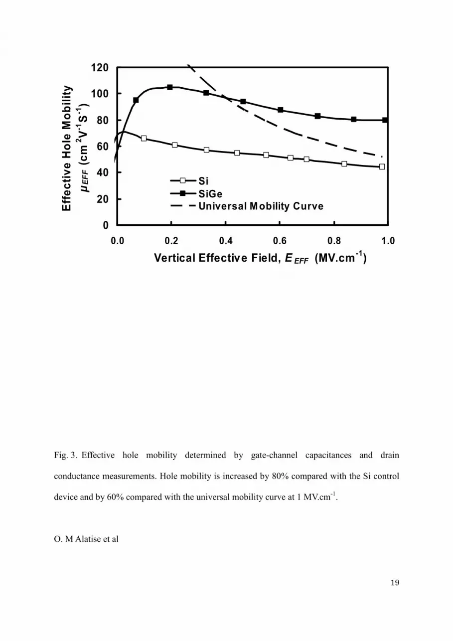
effective mobility was extracted from 1 µm gate length devices. Fig. 3 shows 80% effective
hole mobility (µEFF) enhancement for the strained SiGe devices compared with the Si control

6
device at an effective vertical field (EEFF) of 1 MV.cm-1. The mobility enhancement due to
compressive strain overcomes any mobility reduction caused by the imperfect
SiGe/Si(Ge)ON/HfSiOx interface in the strained SiGe device [8, 23-25] and there is 60%
enhancement in the effective hole mobility compared with the universal mobility curve (Fig.
3) at an EEFF of 1 MV.cm-1. The hole mobility enhancement is greater than that reported in
[13] and [8] where Si0.7Ge0.3 and Si0.8Ge0.2 devices demonstrated 20% hole mobility
enhancement compared with the universal mobility curve at an EEFF of 1 MV.cm-1. The
mobility enhancement in our work is also comparable with that reported in [10] for devices
having higher Ge contents, 28%. Carrier mobilities are affected by the quality of the interface
between the gate dielectric and the channel, especially for high-k/metal gate systems. It is
known that µEFF can be reduced by increased scattering due to the interaction between the
mobile carriers in the channel and charged traps at the interface as well as surface roughness
scattering at high vertical fields. Surface passivation and preparation techniques such as
nitridation prior to dielectric deposition have been shown to improve µEFF in high-k/metal
gate devices by reducing Dit [11, 15-18]. The inclusion of a nitridation step prior to ALD
deposition of the high-k has minimized the impact of Dit on mobility for the devices, as
confirmed by Dit measurements on the devices.
Fig. 4 shows the drain current (IDS) as a function of the drain voltage (VDS) for 1 µm
and 100 nm gate length pMOSFETs at a gate overdrive voltage, VGS-VTH of 0.5 V and 1.0 V.
VGS is the gate voltage and VTH is the threshold voltage. The gate voltage overdrive is used for
IDS comparison because of the lower VTH in the strained SiGe devices as a result of the
reduced bandgap due to the valence band offset [14]. The VTH difference between the devices
reduces from 290 mV at LG =1 µm to 50 mV at LG =100 nm. This is because VTH roll-off is
evident in the Si control devices (VTH(1 µm)=0.71 V and VTH(100 nm)=0.51 V) whereas VTH
remains stable with LG in the strained SiGe devices (VTH(1 µm)=0.42 V and VTH(100 nm)=0.45 V).

7
The output characteristics in Fig. 4 show that the 75% enhancement in the saturation drain
current for the 1 µm gate length strained SiGe device compared with the Si control is lost for
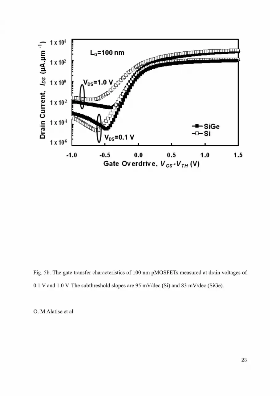
the 100 nm devices. Fig. 5 shows the gate transfer characteristics for the same devices. The
subthreshold slopes are 75 mV/dec (Si) and 83 mV/dec (SiGe) for 1 µm gate length devices
and 95 mV/dec (Si) and 83 mV/dec (SiGe) for 100 nm gate length devices.
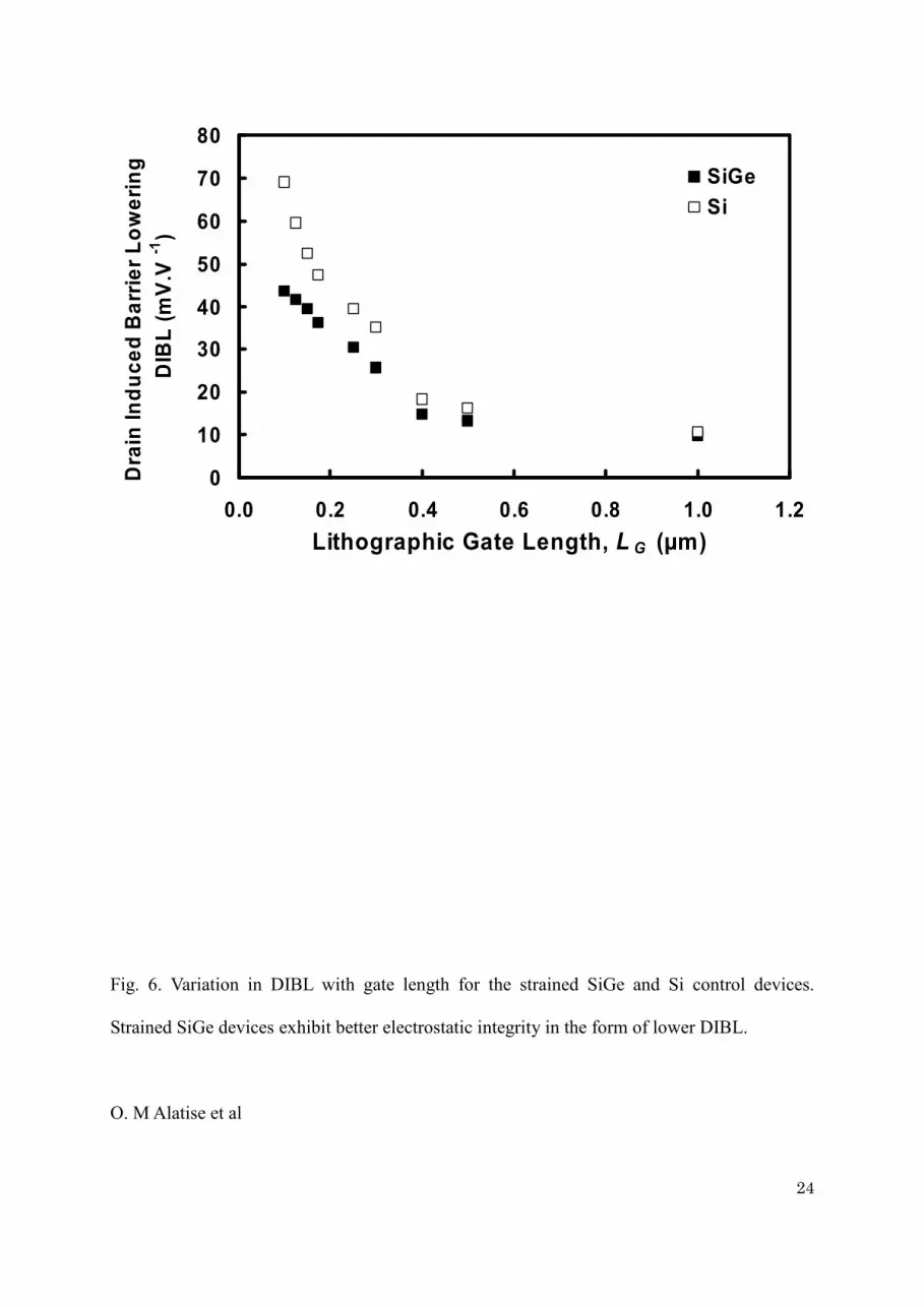
Fig. 6 shows the variation in drain induced barrier lowering (DIBL) with gate length
for the strained SiGe and Si control devices. DIBL is 10 mV/V for both Si and strained SiGe
1 µm devices but increases more rapidly in the scaled Si devices than in the SiGe devices. For
100 nm gate length devices DIBL is 70 mV/V for the Si pMOSFETs and 45 mV/V for the
SiGe pMOSFETs.
The maximum transconductance measured in the SiGe and Si control devices at a
drain voltage of 1 V are presented for a range of lithographic gate lengths (LG) in Fig. 7a.
Performance enhancements for the SiGe devices are presented in Fig. 7b and are shown to
reach 80% compared with Si controls. In agreement with other reports [2-5, 11], Fig. 7b
shows that the enhancements in gmMAX for the strained SiGe devices decrease as the
lithographic gate length is reduced. For LG below 250 nm no enhancement is evident and for
100 nm devices, the Si control outperforms the SiGe devices by approximately 20%.
To enable strained SiGe pMOSFETs to assist in advanced technology nodes, the on-
state performance loss at short lithographic gate lengths must be understood. In this work,
boron is used for the source/drain implants. B is known to have suppressed diffusivity in
compressively strained SiGe compared with bulk Si [26-28], therefore boron will diffuse by
different amounts into the channel region of bulk Si and strained SiGe devices. Consequently
the effective channel length should be used in comparisons of scaled Si and SiGe devices. The
effective channel length, (LEFF), is an electrical parameter that defines the lateral distance
between the source and the drain over which the channel resistivity modulated by the gate-

8
voltage whereas the lithographic gate length (LG) is a physical parameter defined on the mask
layout. The diffusion length (∆L) is defined as the difference between the lithographic gate
length and the effective channel length. The “shift and ratio” method was used to extract the
effective channel length using 1 µm and 0.1 µm gate lengths as the long and short channel
MOSFET, respectively [29]. The effective channel lengths were found to be approximately 65
nm (Si) and 90 nm (SiGe).
The difference in effective channel length of the Si and SiGe devices was also
confirmed using the TCAD process simulator TSUPREM4. The boron implant dose, implant
energies, arsenic halo implant energies, tilt angles, doses and activation anneal temperature-
time cycles used in the TSUPREM process simulation were identical to those used in device
fabrication. Diffusivity data was taken from [28] and the strain was calculated as (1-aGe/aSi)x,
where aGe is the lattice constant of Ge, aSi is the lattice constant of Si and x is the Ge mole
fraction in the SiGe layer. Raman spectroscopy showed that the average compressive strain in
the SiGe channel was about 0.8%, close to the theoretical strain value for 20% Ge. The
diffusivity of boron in compressively strained Si0.77Ge0.23 is ~ OD2.0 where OD is the
diffusivity of boron in unstrained Si [28]. As a first approximation, taking DtL ~∆ where
D is the dopant diffusivity and t is the diffusion time, boron will diffuse approximately 55%
less in the SiGe devices compared with the Si control devices. This difference in diffusion
leads to a shorter metallurgical channel length LMET in the bulk Si devices. The metallurgical
channel length (LMET) is defined as the lateral distance between the source and drain over
which the substrate arsenic doping is higher than the source/drain doping. LMET correlates with
the effective channel length and the lithographic gate length. Fig. 8a shows a 2D profile of B
doping contours in a simulated 100 nm processed device whereas Fig. 8b shows the lateral
cross section of B between the source and drain 5 nm below the MOSFET surface. The
metallurgical channel length is extracted at this position and is found to be approximately 30

9
nm for the Si device and 40 nm for the SiGe device. The effective channel lengths extracted
from I-V data are larger than the metallurgical channel length predicted by the TCAD
simulation. This is expected because the lateral straggle of the junction implants [29] and non-
abrupt source-drain junction profiles effectively shortens the chemical length between the
source and drain. For an ideal junction profile (infinitely abrupt with no lateral straggle), LMET
is larger than LEFF due to sheet resistivity only being modulated by the gate voltage inside the
metallurgical channel. However for a non-abrupt junction profile, there is a fraction of the
channel with the junction implant straggle in accumulation thereby causing LEFF to be larger
than LMET.
Both experimental methods and TCAD process simulations show a shorter effective
and metallurgical channel length for the Si devices compared with the SiGe devices due to
reduced boron diffusivity in compressively strained SiGe. These results also explain the
increased VTH roll-off for the Si devices and Fig. 6, where DIBL is seen to be lower in the
short channel strained SiGe devices than in the Si control devices. Since DIBL relates to the
LEFF through a negative exponential, a small difference in LEFF causes a significant difference
in DIBL [30]. The lower DIBL for the strained SiGe devices therefore correlates as expected
with the stable VTH roll-off, which is usually due to DIBL. Hence, the reduced B diffusion in
compressively strained SiGe results in longer effective channel lengths and better electrostatic
integrity.
The gmMAX data in Fig. 7 are re-evaluated using the effective channel length
calculated by the “shift and ratio” method and are shown in Fig. 9. Using the effective
channel length demonstrates that strained SiGe devices can offer performance enhancements
for all channel lengths greater than 150 nm. In contrast when the devices were analyzed in
terms of their lithographic gate length (Fig. 7) performance gains only appeared possible in
SiGe devices if the gate length exceeded 175 nm.

10
Fig. 9 indicates that for effective channel lengths below 150 nm, the Si control
devices still out-perform the strained SiGe devices. The series resistance (RSD) was also
extracted using the “shift and ratio” method [29] and was found to be 60% higher in the SiGe
devices compared with the Si control devices (80 Ω compared with 50 Ω). The higher RSD in
the strained SiGe devices was confirmed by silicide sheet resistance (RSH) measurements on
test structures, which showed that RSH was approximately 100% higher in the SiGe devices
(8.2 Ω/ in SiGe and 4.2 Ω/ in Si control). Since the silicide anneal process was optimized
for bulk Si and the pMOSFETs have a 40 nm SiGe surface channel layer, high resistance
nickel germanosilicides will have formed due to the presence of Ge [31-33]. It was shown in
[32] that RSH of Ni silicided Si0.75Ge0.25 was 3 Ω/ at 500 °C but increased abruptly at anneal
temperatures above 800 °C. This increase was attributed to the segregation of Ge at the grain
boundaries of nickel germanosilicide during the interfacial reactions between nickel and SiGe.
In [33], nickel silicided Si0.7Ge0.3 and Si0.8Ge0.2 films showed a minimum RSH of 3.9 Ω/ and
3.5 Ω/ respectively at 400 °C. These values are 50% lower than RSH on the SiGe wafers in
this study, and this is likely to be due to the higher annealing temperature used (1000 °C).
However under the appropriate annealing conditions, NiSiGe can offer improved RSH . NiSiGe
can also improve contact resistance because of the reduced barrier height and higher boron
activation compared with NiSi [34, 35].
Process optimization of the silicidation temperature-time cycle for SiGe alloys can
prevent the formation of such high resistance films, therefore it is valid to investigate the
intrinsic device performance without parasitic resistances. The intrinsic drain current was
calculated by correcting for the series resistance using the formula
1
1−
−=
DS
SDDSDSDSO V
RIII (1)

11
where DSOI is the intrinsic drain current. Equation (1) is derived from the strong inversion
MOSFET square law model taking series source/drain resistance into account [19, 36-38].
The resulting intrinsic maximum transconductance data are shown in Fig. 10a. The on-state
performance of the strained SiGe devices is now found to be improved compared with the Si
control devices down to effective gate lengths of 100 nm. The difference between the intrinsic
and measured transconductances increases as the gate length reduces due to the increasing
impact of series parasitic resistance, which becomes a larger proportion of the total channel
resistance in scaled geometries. Comparing the intrinsic gmMAX in Fig. 10a with the measured
gmMAX in Fig. 9a shows that approximately 50% of gm
MAX is lost in scaled SiGe pMOSFETs.
Fig. 10b shows that the intrinsic enhancement in gmMAX of the SiGe devices reaches 80% at
long channel lengths and reduces by only 15% as the effective channel length is scaled from 1
µm to 100 nm. The 65% enhancement in gmMAX at short channel lengths is the highest reported
for SiGe devices using low Ge contents (~20%) to date. In [10], no enhancement in the drain
current compared with the Si control devices was reported for 55 nm strained Si0.72Ge0.28
pMOSFETs and only 15% enhancement in linear transconductance compared with the Si
control was achieved in 130 nm Si0.68Ge0.32 pMOSFETs [3]. In [39], 50 nm gate length
strained Si0.65Ge0.35 pMOSFETs exhibited 35% drive current enhancement compared with Si
controls and in [5] 13% drive current enhancement compared with Si controls was reported in
50 nm strained Si0.72Ge0.28 devices. Our new results suggest that significantly larger
performance gains in strained SiGe pMOSFETs are realizable in deep submicrometer CMOS
technology nodes than previously demonstrated if processing is optimized to take account of
modified dopant diffusion and parasitic series resistance in the SiGe material system.
Fig. 10(b) shows that the intrinsic performance enhancement of short channel strained
SiGe pMOSFETs compared with bulk Si is 15% lower than observed in long channel devices.

12
This reduction may be due self heating arising from the low thermal conductivity of SiGe [40],
strain loss with scaling or the increased impact of halo doping on mobility at short gate
lengths. One of the dominating factors behind the compromised drain current and
transconductance enhancement in scaled strained Si devices fabricated on relaxed SiGe virtual
substrates is self heating [41]. The devices in this study comprise of a 40 nm SiGe surface
layer on a Si substrate rather than a thin Si layer on a thick SiGe layer, thus the impact of self
heating is expected to be considerably lower. AC drain conductance measurements which
remove self-heating effects [42] were carried out on 100 nm strained SiGe devices. Fig. 11
shows there is an increase in drain current compared with DC conditions of only ~3% for the
SiGe device when measurements were carried out at 10 MHz. Therefore self heating is not a
performance limiting mechanism in scaled strained SiGe pMOSFET devices.
Potential variations in mobility with gate length may also impact performance gains
in scaled devices. Unintentional fluctuations in channel strain with gate length scaling due to
stresses induced during epitaxial growth, from the silicide and trench isolation may counteract
the intentional channel strain. Strain relaxation in the SiGe layers at the source/drain regions
may also result from defects caused by ion implantation. These defects together with the loss
of strain can cause additional carrier scattering thereby contributing to mobility reduction.
Electrically, the impact of these defects and strain relaxation will be manifested as increased
series resistance and its relative impact would also increase as the gate length is scaled. Since
strain relaxation at nanoscale dimensions cannot be characterised electrically, it is not possible
to accurately separate its effect from that of increased series resistance due to silicide sheet
resistance. At present the limited availability of nanoscale strain characterization techniques
prevents a full understanding of the impact of various strain contributions in deep
submicrometer CMOS.

13
IV. SUMMARY
The scalability of high performance strained SiGe pMOSFETs with HfSiOx/TiSiN
gate stacks has been examined. The intrinsic performance of short channel SiGe devices has
been shown to exceed that of co-processed Si controls by as much as 65% in 100 nm devices,
whereas extrinsic gains are completely diminished for drawn gate lengths below 175 nm.
Performance enhancements exceeding 70% in both long and short channel devices are the
highest reported gains to date compared with bulk Si using just 20% Ge in the channel region.
The dominating factors behind the compromised performance gains observed in the measured
short channel strained SiGe devices are found to be differences in the effective channel length
due to strain altered dopant diffusion and increased parasitic series resistance. Self heating
due to the low thermal conductivity of SiGe was analyzed and shown to have a smaller impact
on scaled device performance (~3%). The intrinsic potential of the devices was assessed by
correcting for the differing effective channel lengths and source-drain series resistance. After
correction, 65% of the long-channel strain induced performance enhancement was maintained
at scaled geometries. The work presented suggests a major underestimation of the potential of
SiGe for advanced technology nodes. The effective channel length of SiGe devices was 40%
larger than that of the Si controls for 100 nm lithographic gate lengths due to suppressed
boron diffusivity from the source/drain regions in SiGe. This difference was confirmed by
TCAD simulations that showed a 30% increase in the metallurgical channel length for 100 nm
SiGe devices. The source-drain series resistance was also 70% higher in the SiGe devices due
to silicidation being optimized for bulk Si. While electrical results are convincing, direct
comparisons between LEFF and RSD matched strained SiGe and Si pMOSFETs would be even
more reliable in evaluating the scalability of the performance enhancements in compressively
strained SiGe devices. However, this comparison is only possible if the respective thermal

14
processes of the devices are customized. The work shows that strained SiGe pMOSFETs are
scalable and are suitable for deep submicrometer CMOS technology nodes if series resistance
and dopant diffusion can be controlled.
ACKNOWLEDGEMENTS
This work is financially supported by EPSRC (UK) and SEMATECH (USA).

15
REFERENCES [1] S. H. Olsen, A. G. O'Neill, S. Chattopadhyay, L. S. Driscoll, K. S. K. Kwa, D. Norris, A. Cullis, and D. J.
Paul, "Study of single and dual channel designs of high performance strained Si/SiGe n-MOSFETs," IEEE Trans. Electron Devices, vol. 51, pp. 1245-1253, 2004.
[2] V. Kesan, S. Subbanna, P. Restle, M. Tejwani, J. Altken, S. Lyer, and J. Ott, "High performance 0.25 um pMOSFETs with Silicon-Germanium channels for 300K and 77K operation," in IEDM Tech. Dig., pp. 25-28, 1991.
[3] N. Collaert, P. Verheyen, K. Meyer, R. Loo, and M. Caymax, "High performance Si/SiGe pMOSFETs fabricated in a standard CMOS process technology," Solid State Electron., vol. 47, pp. 1173-1177, 2003.
[4] A. Lindgren, P. Hellberg, M. Haartman, D. Wu, C. Menon, S. Zhang, and M. Ostling, "Enhanced intrinsic gain of pMOSFETs with SiGe channel," in Proc. ESSDERC, pp. 175-178, 2002.
[5] R. Loo, N. Collaert, P. Verheyen, M. Caymax, R. Delhougne, and K. Meyer, "Fabrication of 50 nm high performance strained SiGe pMOSFETs with selective epitaxial growth," Appl. Surf. Sci., vol. 224, pp. 292-296, 2004.
[6] S. Maikap, J. Lee, D. Yim, R. Mahapatra, S. Ray, J. Song, Y. No, and W. Choi, "Physical and electrical properties of ultrathin HfO2/HfSixOy stacked gate dielectrics on compressively strained Si0.74Ge0.26/Si heterolayers," J. Vac. Sci. Technol. B, vol. 22, pp. 52-56, 2003.
[7] C. Maiti, S. Maikap, S. Chatterjee, S. Nandi, and S. Samanta, "Hafnium oxide gate dielectric for Si1-
xGex," Solid State Electron., vol. 47, pp. 1995-2000, 2003. [8] Z. Shi, D. Onsongo, K. Onishi, J. Lee, and S. Banerjee, "Mobility enhancement in surface channel SiGe
PMOSFETs With HfO2 gate dielectrics," IEEE Electron Device Lett., vol. 24, pp. 34-36, January 2003 2003.
[9] Z. Shi, D. Onsongo, and S. Banerjee, "Mobility and performance enhancement on compressively strained SiGe channel pMOSFETs," Appl. Surf. Sci, vol. 224, pp. 248-253, 2004.
[10] O. Weber, F. Ducroquet, T. Ernst, F. Andrieu, J. Damlencourt, J. Hartmann, B. Guillamourt, A. Papon, H. Danas, L. Brevard, A. Toffoli, P. Besson, F. Martin, Y. Morand, and S. Delonibus, "55 nm high mobility SiGe(:C) with HfO2 gate dielectric and TiN metal gate for advanced CMOS," in symp. on VLSI Tech. Dig., pp. 42-43, 2004.
[11] O. Weber, J. Damlencourt, F. Andrieu, and F. Ducroquet, "Fabrication and mobility characterisitics of SiGe surface channel pMOSFETs with HfO2/TiN gate stack," IEEE Trans. Electron Devices, vol. 53, pp. 449-456, March 2006 2006.
[12] D. Wu, S. Person, A. Lindgren, G. Sjoblom, P. Hellstrom, J. Olsson, S. Zhang, M. Ostling, E. Ahlgren, W. Li, and M. Touminen, "ALD Metal Gate/High K Gate Stack for Si and SiGe Surface Channel P-MOSFETs."
[13] D. Wu, J. Lu, H. Radamson, P. Hellstrom, Q. Zhang, M. Ostling, E. Ahlgren, E. Tois, and M. Tuominen, "Influence of surface treatment prior to ALD high k dielectrics on the performance of SiGe surface channel pMOSFETs," IEEE Electron Device Lett., vol. 25, pp. 289-291, May 2004 2004.
[14] H Harris, P Kalra, P Majhi, M Hussain, D Kelly, J Oh, D He, C Smith, J Barnett, P Kirsch, G Gebara, J Jur, T Ma, G Sung, S Thompson, B Lee, H Tseng, and R. Jammy, "Band engineered low PMOS Vt with high-k/metal gate featured in a dual channel CMOS integration scheme," in symp. on VLSI Tech. Dig., pp. 154-155, 2007.
[15] O. Sullivan, V. Kaushik, J. Everaert, L. Trojan, L. Ragnarsson, L. Pantisano, E. Rohr, S. DeGendt, and M. Heyns, "Effectiveness of Nitridation of Hafnium Silicate Dielectrics: A Comparison Between Thermal and Plasma Nitridation," IEEE Trans. Electron Devices, vol. 54, pp. 1771-1775, 2007.
[16] G. Nicholas, D. Brunco, A. Dimoulas, J. Steenbergen, F. Bellenger, M. Houssa, M. Caymax, M. Meuris, Y. Panayiotatos, and A. Sotiropoulus, "Germanium MOSFETs with CeO2/HfO2/TiN gate stacks," IEEE Trans. Electron Devices, vol. 54, pp. 1425-1430, June 2007 2007.
[17] N. Wu, Q. Zhang, N. Balasubramanian, D. Chan, and C. Zhu, "Characterisitics of Self Aligned Gate First Ge p and n Channel MOSFETs Using CVD HfO2 Gate Dielectric and Si Surface Passivation," IEEE Transactions on Electron Devices, vol. 54, pp. 733-741, April 2007 2007.
[18] K. Onishi, C. Kang, R. Choi, H. Cho, and S. Gopalan, "Improvement of surface carrier Mobility of HfO2 MOSFETs by high temperature forming gas annealing," IEEE Trans. Electron Devices, vol. 50, pp. 384-390, February 2003 2003.
[19] D. Schroeder, "Semiconductor material and device characterization," Wiley, 1998. [20] G. Dalapati, S. Chattopadhyay, K. Kwa, S. Olsen, Y. Tsang, R. Agaiby, A. O'Neill, P. Dobrosz, and S.
Bull, "Impact of strained Si thickness and Ge out-diffusion on gate oxide quality for strained Si surface channel n-MOSFETs," IEEE Trans. Electron Devices, vol. 53, pp. 1142-1152, 2006.
[21] K. Kwa, S. Chattopadhyay, S. Olsen, A. O'Neill, L. Driscoll, and A. O'Neill, "Optimisation of channel

16
thickness in Strained Si/SiGe MOSFETs," in Proc. ESSDERC, 2003. [22] M. Hartman, G. Malm, and M. Ostling, "Comprehensive Study of Low Frequency Noise and Mobility
in Si and SiGe pMOSFETs with High-k Gate Dielectrics and TiN Gate," Trans Electron Dev, vol. 53, pp. 836-843, 2006.
[23] S. Datta, J. Brask, G. Dewey, M. Doczy, B. Doyle, B. Jin, J. Kavalieros, M. Metz, A. Majumdar, M. Radosavljevic, and R. Chau, "Advanced Si and SiGe strained channel NMOS and PMOS transistors with high k/metal gate stack," IEEE BCTM, vol. 194-197, 2004.
[24] B. Guillaumot, X. Garros, F. Lime, K. Oshima, B. Tavel, P. Masson, T. Tuche, A. Papn, J. Damlencourt, S. Maitrejean, M. Rivoire, C. Leroux, S. Christoloveanu, G. Ghibaudo, J. Autran, T. Stotnicki, and S. Deleonibus, "75 nm damascene metal gate and high k integration for advanced CMOS devices," in IEDM Tech. Dig., 2002.
[25] F. Lime, K. Oshima, M. Casse, G. Ghibaudo, S. Christoloveanu, B. Guillamourt, and H. Iwai, "Carrier mobility in advanced CMOS devices with metal gate and HfO2 gate dielectric," Solid State Electron., vol. 47, pp. 1617-1621, 2003.
[26] K. Rajendran and W. Schoenmaker, "Studies of boron diffusivity in strained SiGe epitaxial layers," J. Appl. Phys., vol. 89, pp. 980-987, 2001.
[27] N Zangenberg, J Pedersen, J Hansen, and N. Larsen, "Boron and phosphorus diffusion in strained and relaxed Si and SiGe," J. Appl. Phys., vol. 94, pp. 3883-3890, 15 September 2003 2003.
[28] N Cowern, P Zalm, P Van der Sluis, D Gravesteijn, and W. Boer, "Diffusion in strained Si(Ge)," Phys. Rev. Lett., vol. 72, pp. 2585-2588, 30 November 1994 1994.
[29] Y. Taur, "MOSFET channel length: extraction and interpretation," IEEE Trans. Electron Devices, vol. 47, pp. 160-169, 2000.
[30] J Huang, Z Liu, M Jeng, P Ko, and C. Hu, "A physical model for MOSFET output resistance," in IEDM Tech. Dig., pp. 569-572, 1992.
[31] J Liu and M. Ozturk, "Nickel germanosilicide contacts formed on heavily boron doped SiGe sourcedrain junctions for nanoscale CMOS," IEEE Trans. Electr. Devices, vol. 52, pp. 1535-1540, 2005.
[32] K Pey, W Choi, S Chattopadhyay, H Zhao, F Fitzgerald, and D. Antoniadis, "Thermal reaction of nickel and SiGe alloy," J. Vac. Sci. Technol, vol. 20, pp. 1903-1910, 2002.
[33] A Saha, S Chattopadhyay, and C. Maiti, "Contact metallization on strained Si," Solid State Electron., vol. 48, pp. 1391-1399, 2004.
[34] S. Zhang, "Nickel based contact metallization for SiGe MOSFETs: progress and challenges," Microelectronic Engineering, vol. 70, pp. 174-185, 2003.
[35] J. Shim, H. Oh, H. Choi, T. Sakaguchi, H. Kurino, and M. Koyanagi, "SiGe elevated source/drain structure and nickel contact layer for 0.1 um MOSFET fabrication," Appl. Surf. Sci, vol. 224, pp. pp 260-264, 2004.
[36] K. Lim and X. Zhou, "A Physically Based Semi-Empirical Series Resistance Model for Deep-Submicron MOSFET I-V Modelling," IEEE Trans. Electron Devices, vol. 47, pp. 1300-1302, 2000.
[37] R. Langevelde and F. Klaassen, "Effect of gate field dependent mobility degradation on distortion analysis in MOSFETs," IEEE Trans. Electron Devices, vol. 44, pp. 2044-2052, 1997.
[38] K. Rim, J. Hoyt, and J. Gibbons, "Analysis and fabrication deep submicron strained Si n-MOSFETs," IEEE Trans. Electron Devices, vol. 47, pp. 1406-1415, 2000.
[39] K. Ikeda, Y. Yamashitta, A. Endoh, T. Fukano, K. Hikosaka, and T. Mimura, "50 nm gate schottky source/drain pMOSFETs with a SiGe channel," IEEE Electron Device Lett., vol. 23, pp. 670-672, 2002.
[40] J. Dismukes, L. Ekstrom, E. Steigmeier, I. Kudman, and D. Beers, "Thermal and electrical properties of heavily doped Ge-Si alloys up to 1300 K," J. Appl. Phys., vol. 35, pp. 2899-2907, 1964.
[41] R. Agaiby, Y. Yang, S. H. Olsen, A. G. O'Neill, G. Eneman, P. Verheyen, R. Loo, and C. Claeys, "Quantifying Self-Heating Effects with Scaling in Globally Strained Si MOSFETs," Solid-State Electron., vol. 51, pp. 1473-1478, 2007/0 2007.
[42] W Jin, W Liu, S Fung, P Chan, and C. Hu, "SOI thermal impedance extraction methodology and its significance for circuit simulation," IEEE Trans. Electron Devices, vol. 48, pp. 730-736, 2001.

17
Fig. 1. TEM images of a 70 nm strained SiGe device and the corresponding gate
stack/channel.
O. M Alatise et al

18
Fig. 2. The distribution of device performance for the 1 µm gate length strained SiGe and the
Si control pMOSFETs. gmMAX is measured at a drain voltage of 1 V.
O. M Alatise et al
19
Fig. 3. Effective hole mobility determined by gate-channel capacitances and drain
conductance measurements. Hole mobility is increased by 80% compared with the Si control
device and by 60% compared with the universal mobility curve at 1 MV.cm-1.
O. M Alatise et al
0
20
40
60
80
100
120
0.0 0.2 0.4 0.6 0.8 1.0
Vertical Effective Field, E EFF (MV.cm -1)
Eff
ecti
ve H
ole
Mo
bili
ty
µE
FF
(cm
2 V-1
S-1
)
SiSiGeUniversal Mobility Curve

20
Fig. 4a. Drain current output characteristics of 1 µm pMOSFETs measured at a gate overdrive
voltage (VGS-VTH) of 0.5 V and 1.0 V. At a drain voltage of 1 V for both gate overdrives, the
drain current is increased by 75% for the strained SiGe pMOSFETs compared with the Si
control.
O. M Alatise et al
0
20
40
60
80
100
0.0 0.2 0.4 0.6 0.8 1.0
Drain Voltage, V DS (V)
Dra
in C
urr
ent,
ID
S (
µA.µ
m-1
)SiSiGe
VGS-VTH= 1.0 V
VGS-VTH=0.5 V
LG=1 µm

21
Fig. 4b. Drain current output characteristics of 100 nm pMOSFETs measured at a gate
overdrive voltage (VGS-VTH) of 0.5 V and 1.0 V. The Si control exhibits higher drain current
than the strained SiGe device.
O. M Alatise et al
0
80
160
240
320
400
480
560
640
720
0.0 0.2 0.4 0.6 0.8 1.0Drain Voltage, V DS (V)
Dra
in C
urr
ent,
I D
S (
µA.µ
m-1
)SiSiGe
VGS-VTH=0.5 V
VGS-VTH= 1.0 V
LG=100 nm

22
Fig. 5a. The gate transfer characteristics of 1 µm pMOSFETs measured at drain voltages of
0.1 V and 1.0 V. The subthreshold slopes are 75 mV/dec (Si) and 83 mV/dec (SiGe).
O. M Alatise et al
23
Fig. 5b. The gate transfer characteristics of 100 nm pMOSFETs measured at drain voltages of
0.1 V and 1.0 V. The subthreshold slopes are 95 mV/dec (Si) and 83 mV/dec (SiGe).
O. M Alatise et al
24
Fig. 6. Variation in DIBL with gate length for the strained SiGe and Si control devices.
Strained SiGe devices exhibit better electrostatic integrity in the form of lower DIBL.
O. M Alatise et al
0
10
20
30
40
50
60
70
80
0.0 0.2 0.4 0.6 0.8 1.0 1.2
Lithographic Gate Length, L G (µm)
Dra
in In
du
ced
Bar
rier
Lo
wer
ing
D
IBL
(mV
.V-1
)SiGeSi

25
Fig. 7a. Variation in measured maximum transconductance with lithographic gate length for
the Si and SiGe devices. The performance gains of the SiGe devices compared with the Si
devices evident at large lithographic gate lengths are diminished at gate lengths below ~ 200
nm.
O. M Alatise et al
0
100
200
300
400
500
600
700
800
0.0 0.2 0.4 0.6 0.8 1.0 1.2
Lithographic Gate Length, L G (µm)
Mea
sure
d M
axim
um
T
ran
sco
ndu
ctan
ce
gm
MA
X (
mS
.mm
-1) Si
SiGe
Crossover point
VDS=1 V

26
Fig. 7b. The percentage enhancement in maximum transconductance of the SiGe devices
compared with the Si controls. Devices were measured at a drain voltage of 1 V.
O. M Alatise et al
-25
0
25
50
75
100
0.0 0.2 0.4 0.6 0.8 1.0 1.2
Lithographic Gate Length, L G (µm)
% E
nh
ance
men
t in
Max
imu
m
Tra
nsc
on
du
ctan
ce (
gm
MA
X)
ove
r S
i Co
ntr
ol
VDS=1 V

27
Fig. 8a. The processed device simulated in TSUPREM4 using the actual process parameters.
The solid and dashed lines represent contours of boron concentration after annealing and
show the extent of boron diffusion.
O. M Alatise et al

28
Fig. 8b. Simulated boron concentration 5 nm below the 100 nm MOSFET surface. The boron
concentration in the channel is lower in the SiGe devices due to retarded boron diffusivity in
compressively strained SiGe compared with bulk Si.
O. M Alatise et al
0.0
0.5
1.0
1.5
2.0
2.5
0.1 0.2 0.3 0.4 0.5 0.6
MOSFET Lateral Profile (µm)
Act
ive
Bo
ron
Co
nce
ntr
atio
n
(x10
20cm
-3)
SiSiGeIdeal
Source Drain Gate

29
Fig. 9a. Variation in the measured maximum transconductance with effective channel length
for Si and SiGe devices. Performance gains are demonstrated down to smaller gate lengths
when the effective channel length is used instead of the lithographic gate length. The devices
were measured at a drain voltage of 1 V.
O. M Alatise et al
0
100
200
300
400
500
600
700
800
0.0 0.2 0.4 0.6 0.8 1.0Effective Channel Length, L EFF (µm)
Mea
sure
d M
axim
um
T
ran
sco
nd
uct
ance
g
mM
AX
(mS
.mm
-1)
SiSiGe
VDS=1 V
Crossover point

30
Fig. 9b. Percentage enhancement in measured maximum transconductance for the strained Si
devices compared with the Si control devices for a range of effective channel lengths. The
devices were measured at a drain voltage of 1 V.
O. M Alatise et al
-20
0
20
40
60
80
100
0.0 0.2 0.4 0.6 0.8 1.0 1.2
Effective Channel Length, L EFF (µm)
% E
nh
ance
men
t in
Max
imu
m
Tra
nsc
on
du
ctan
ce (
gm
MA
X)
ove
r S
i Co
ntr
ol
VDS=1 V

31
Fig. 10a. Variation in intrinsic maximum transconductance with effective channel length for
the Si and SiGe pMOSFETs.
O. M Alatise et al
0
200
400
600
800
1000
1200
1400
1600
0.0 0.2 0.4 0.6 0.8 1.0Effective Channel Length, L EFF (µm)
Intr
insi
c M
axim
um
T
ran
sco
nd
uct
ance
g
mIN
TM
AX
(m
S.m
m-1
)Si
SiGe
VDS=1 V

32
Fig. 10b. Percentage enhancement in the intrinsic maximum transconductance for the strained
SiGe devices compared with the Si control devices. The enhancement of the intrinsic SiGe
device is only reduced by ~ 15% as the effective channel length is scale from 1 µm to 100 nm.
O. M Alatise et al
0
10
20
30
40
50
60
70
80
90
0.0 0.2 0.4 0.6 0.8 1.0 1.2
Effective Channel Length, L EFF (µm)
% E
nh
ance
men
t in
Max
imu
m
Tra
nsc
on
du
ctan
ce (
gm
MA
X)
ove
r S
i Co
ntr
ol VDS=1 V

33
Fig.11. Output characteristics for 100 nm gate length SiGe pMOSFETs measured at a gate
overdrive voltage (VGS-VTH) = 1.5 V at DC and 10 MHz. The 3% difference in drain current
measured at a drain voltage of 1.5 V using DC and 10 MHz conditions is proportional to
device self heating and is considered negligible in the strained SiGe devices.
O. M Alatise et al
0
100
200
300
400
500
600
0.00 0.25 0.50 0.75 1.00 1.25 1.50 1.75 2.00
Drain Voltage, V DS (V)
Dra
in C
urr
ent,
I DS
(µA
.µm
-1) DC
10 MHz
LG=100 nm VGS-VTH=1.5 V
3% difference in IDSAT

34
Fig. 1. TEM images of a 70 nm strained SiGe device and the corresponding gate
stack/channel.
Fig. 2. The distribution of device performance for the 1 µm gate length strained SiGe and the
Si control pMOSFETs.
Fig. 3. Effective hole mobility determined by gate-channel capacitances and drain
conductance measurements. Hole mobility is increased by 80% compared with the Si control
device and by 60% compared with the universal mobility curve at 1 MV.cm-1.
Fig. 4a. Drain current output characteristics of 1 µm pMOSFETs measured at a gate overdrive
voltage (VGS-VTH) of 0.5 V and 1.0 V. At a drain voltage of 1 V for both gate overdrives, the
drain current is increased by 75% for the strained SiGe pMOSFETs compared with the Si
control.
Fig. 4b. Drain current output characteristics of 100 nm pMOSFETs measured at a gate
overdrive voltage (VGS-VTH) of 0.5 V and 1.0 V. The Si control exhibits higher drain current
than the strained SiGe device.
Fig. 5a. The gate transfer characteristics of 1 µm pMOSFETs measured at drain voltages of
0.1 V and 1.0 V. The subthreshold slopes are 75 mV/dec (Si) and 83 mV/dec (SiGe).
Fig. 5b. The gate transfer characteristics of 100 nm pMOSFETs measured at drain voltages of
0.1 V and 1.0 V. The subthreshold slopes are 95 mV/dec (Si) and 83 mV/dec (SiGe).
35
Fig. 6. Variation in DIBL with gate length for the strained SiGe and Si control devices.
Strained SiGe devices exhibit better electrostatic integrity in the form of lower DIBL.
Fig. 7a. Variation in measured maximum transconductance with lithographic gate length for
the Si and SiGe devices. The performance gains of the SiGe devices compared with the Si
devices evident at large lithographic gate lengths are diminished at gate lengths below ~ 200
nm.
Fig. 7b. The percentage enhancement in maximum transconductance of the SiGe devices
compared with the Si controls. Devices were measured at a drain voltage of 1 V.
Fig. 8a. The processed device simulated in TSUPREM4 using the actual process parameters.
The solid and dashed lines represent contours of boron concentration after annealing and
show the extent of boron diffusion.
Fig. 8b. Simulated boron concentration 5 nm below the 100 nm MOSFET surface. The boron
concentration in the channel is lower in the SiGe devices due to retarded boron diffusivity in
compressively strained SiGe compared with bulk Si.
Fig. 9a. Variation in the measured maximum transconductance with effective channel length
for Si and SiGe devices. Performance gains are demonstrated down to smaller gate lengths
when the effective channel length is used instead of the lithographic gate length. The devices
were measured at a drain voltage of 1 V.
Fig. 9b. Percentage enhancement in measured maximum transconductance for the strained Si

36
devices compared with the Si control devices for a range of effective channel lengths. The
devices were measured at a drain voltage of 1 V.
Fig. 10a. Variation in intrinsic maximum transconductance with effective channel length for
the Si and SiGe pMOSFETs.
Fig. 10b. Percentage enhancement in the intrinsic maximum transconductance for the strained
SiGe devices compared with the Si control devices. The enhancement of the intrinsic SiGe
device is only reduced by ~ 15% as the effective channel length is scale from 1 µm to 100 nm.
Fig.11. Output characteristics for 100 nm gate length SiGe pMOSFETs measured at a gate
overdrive voltage (VGS-VTH) = 1.5 V at DC and 10 MHz. The 3% difference in drain current
measured at a drain voltage of 1.5 V using DC and 10 MHz conditions is proportional to
device self heating and is considered negligible in the strained SiGe devices.


